EP2878943A1 - Void-arranged structure and measurement method using same - Google Patents
Void-arranged structure and measurement method using same Download PDFInfo
- Publication number
- EP2878943A1 EP2878943A1 EP13822692.3A EP13822692A EP2878943A1 EP 2878943 A1 EP2878943 A1 EP 2878943A1 EP 13822692 A EP13822692 A EP 13822692A EP 2878943 A1 EP2878943 A1 EP 2878943A1
- Authority
- EP
- European Patent Office
- Prior art keywords
- array structure
- aperture array
- principal surface
- aperture
- specimen
- Prior art date
- Legal status (The legal status is an assumption and is not a legal conclusion. Google has not performed a legal analysis and makes no representation as to the accuracy of the status listed.)
- Withdrawn
Links
- 238000000691 measurement method Methods 0.000 title claims description 24
- 238000000034 method Methods 0.000 claims abstract description 10
- 230000001154 acute effect Effects 0.000 claims description 5
- 238000005259 measurement Methods 0.000 description 29
- 230000035945 sensitivity Effects 0.000 description 14
- 239000004065 semiconductor Substances 0.000 description 12
- 230000008859 change Effects 0.000 description 11
- 238000000411 transmission spectrum Methods 0.000 description 11
- PXHVJJICTQNCMI-UHFFFAOYSA-N Nickel Chemical compound [Ni] PXHVJJICTQNCMI-UHFFFAOYSA-N 0.000 description 10
- 230000000737 periodic effect Effects 0.000 description 10
- 238000002834 transmittance Methods 0.000 description 10
- 229910052751 metal Inorganic materials 0.000 description 8
- 239000002184 metal Substances 0.000 description 8
- 102000004169 proteins and genes Human genes 0.000 description 6
- 108090000623 proteins and genes Proteins 0.000 description 6
- 150000001875 compounds Chemical class 0.000 description 5
- 230000003247 decreasing effect Effects 0.000 description 5
- 238000010586 diagram Methods 0.000 description 5
- 230000005672 electromagnetic field Effects 0.000 description 5
- 229910052759 nickel Inorganic materials 0.000 description 5
- 239000000126 substance Substances 0.000 description 5
- 230000005540 biological transmission Effects 0.000 description 4
- 230000000052 comparative effect Effects 0.000 description 4
- 230000007423 decrease Effects 0.000 description 4
- 230000000694 effects Effects 0.000 description 4
- PCHJSUWPFVWCPO-UHFFFAOYSA-N gold Chemical compound [Au] PCHJSUWPFVWCPO-UHFFFAOYSA-N 0.000 description 4
- 229910052737 gold Inorganic materials 0.000 description 4
- 239000010931 gold Substances 0.000 description 4
- 238000001228 spectrum Methods 0.000 description 4
- 125000003396 thiol group Chemical group [H]S* 0.000 description 4
- 229910001218 Gallium arsenide Inorganic materials 0.000 description 3
- 239000013078 crystal Substances 0.000 description 3
- 125000000524 functional group Chemical group 0.000 description 3
- 230000006872 improvement Effects 0.000 description 3
- 230000010287 polarization Effects 0.000 description 3
- 238000001328 terahertz time-domain spectroscopy Methods 0.000 description 3
- VYZAMTAEIAYCRO-UHFFFAOYSA-N Chromium Chemical compound [Cr] VYZAMTAEIAYCRO-UHFFFAOYSA-N 0.000 description 2
- RYGMFSIKBFXOCR-UHFFFAOYSA-N Copper Chemical compound [Cu] RYGMFSIKBFXOCR-UHFFFAOYSA-N 0.000 description 2
- 108020004414 DNA Proteins 0.000 description 2
- 102000053602 DNA Human genes 0.000 description 2
- 238000005033 Fourier transform infrared spectroscopy Methods 0.000 description 2
- XEEYBQQBJWHFJM-UHFFFAOYSA-N Iron Chemical compound [Fe] XEEYBQQBJWHFJM-UHFFFAOYSA-N 0.000 description 2
- BQCADISMDOOEFD-UHFFFAOYSA-N Silver Chemical compound [Ag] BQCADISMDOOEFD-UHFFFAOYSA-N 0.000 description 2
- 108020004682 Single-Stranded DNA Proteins 0.000 description 2
- 229910007709 ZnTe Inorganic materials 0.000 description 2
- 229910052804 chromium Inorganic materials 0.000 description 2
- 239000011651 chromium Substances 0.000 description 2
- 239000004020 conductor Substances 0.000 description 2
- 229910052802 copper Inorganic materials 0.000 description 2
- 239000010949 copper Substances 0.000 description 2
- 238000001514 detection method Methods 0.000 description 2
- 229910052732 germanium Inorganic materials 0.000 description 2
- 125000002887 hydroxy group Chemical group [H]O* 0.000 description 2
- 239000000463 material Substances 0.000 description 2
- 229910052710 silicon Inorganic materials 0.000 description 2
- 229910052709 silver Inorganic materials 0.000 description 2
- 239000004332 silver Substances 0.000 description 2
- XUIMIQQOPSSXEZ-UHFFFAOYSA-N Silicon Chemical compound [Si] XUIMIQQOPSSXEZ-UHFFFAOYSA-N 0.000 description 1
- 229910000577 Silicon-germanium Inorganic materials 0.000 description 1
- RTAQQCXQSZGOHL-UHFFFAOYSA-N Titanium Chemical compound [Ti] RTAQQCXQSZGOHL-UHFFFAOYSA-N 0.000 description 1
- 229910045601 alloy Inorganic materials 0.000 description 1
- 239000000956 alloy Substances 0.000 description 1
- 125000003277 amino group Chemical group 0.000 description 1
- 239000000427 antigen Substances 0.000 description 1
- 102000036639 antigens Human genes 0.000 description 1
- 108091007433 antigens Proteins 0.000 description 1
- 230000008901 benefit Effects 0.000 description 1
- 125000003178 carboxy group Chemical group [H]OC(*)=O 0.000 description 1
- 239000000919 ceramic Substances 0.000 description 1
- 239000012141 concentrate Substances 0.000 description 1
- 230000005611 electricity Effects 0.000 description 1
- 239000000835 fiber Substances 0.000 description 1
- 230000005251 gamma ray Effects 0.000 description 1
- GNPVGFCGXDBREM-UHFFFAOYSA-N germanium atom Chemical compound [Ge] GNPVGFCGXDBREM-UHFFFAOYSA-N 0.000 description 1
- 229910052739 hydrogen Inorganic materials 0.000 description 1
- 239000001257 hydrogen Substances 0.000 description 1
- 230000001771 impaired effect Effects 0.000 description 1
- 229910052742 iron Inorganic materials 0.000 description 1
- 239000003446 ligand Substances 0.000 description 1
- 150000002632 lipids Chemical class 0.000 description 1
- 230000004807 localization Effects 0.000 description 1
- 239000011159 matrix material Substances 0.000 description 1
- QSHDDOUJBYECFT-UHFFFAOYSA-N mercury Chemical compound [Hg] QSHDDOUJBYECFT-UHFFFAOYSA-N 0.000 description 1
- 229910052753 mercury Inorganic materials 0.000 description 1
- 150000002739 metals Chemical class 0.000 description 1
- 238000012986 modification Methods 0.000 description 1
- 230000004048 modification Effects 0.000 description 1
- 230000003287 optical effect Effects 0.000 description 1
- 239000002245 particle Substances 0.000 description 1
- 238000012545 processing Methods 0.000 description 1
- 238000011002 quantification Methods 0.000 description 1
- 238000000985 reflectance spectrum Methods 0.000 description 1
- 230000004044 response Effects 0.000 description 1
- 229910052594 sapphire Inorganic materials 0.000 description 1
- 239000010980 sapphire Substances 0.000 description 1
- SBIBMFFZSBJNJF-UHFFFAOYSA-N selenium;zinc Chemical compound [Se]=[Zn] SBIBMFFZSBJNJF-UHFFFAOYSA-N 0.000 description 1
- 239000010703 silicon Substances 0.000 description 1
- 239000007787 solid Substances 0.000 description 1
- 230000001360 synchronised effect Effects 0.000 description 1
- 239000010936 titanium Substances 0.000 description 1
- 229910052719 titanium Inorganic materials 0.000 description 1
Images


Classifications
-
- G—PHYSICS
- G01—MEASURING; TESTING
- G01N—INVESTIGATING OR ANALYSING MATERIALS BY DETERMINING THEIR CHEMICAL OR PHYSICAL PROPERTIES
- G01N21/00—Investigating or analysing materials by the use of optical means, i.e. using sub-millimetre waves, infrared, visible or ultraviolet light
- G01N21/17—Systems in which incident light is modified in accordance with the properties of the material investigated
- G01N21/25—Colour; Spectral properties, i.e. comparison of effect of material on the light at two or more different wavelengths or wavelength bands
- G01N21/31—Investigating relative effect of material at wavelengths characteristic of specific elements or molecules, e.g. atomic absorption spectrometry
- G01N21/35—Investigating relative effect of material at wavelengths characteristic of specific elements or molecules, e.g. atomic absorption spectrometry using infrared light
- G01N21/3581—Investigating relative effect of material at wavelengths characteristic of specific elements or molecules, e.g. atomic absorption spectrometry using infrared light using far infrared light; using Terahertz radiation
- G01N21/3586—Investigating relative effect of material at wavelengths characteristic of specific elements or molecules, e.g. atomic absorption spectrometry using infrared light using far infrared light; using Terahertz radiation by Terahertz time domain spectroscopy [THz-TDS]
-
- G—PHYSICS
- G01—MEASURING; TESTING
- G01N—INVESTIGATING OR ANALYSING MATERIALS BY DETERMINING THEIR CHEMICAL OR PHYSICAL PROPERTIES
- G01N21/00—Investigating or analysing materials by the use of optical means, i.e. using sub-millimetre waves, infrared, visible or ultraviolet light
- G01N21/01—Arrangements or apparatus for facilitating the optical investigation
-
- G—PHYSICS
- G02—OPTICS
- G02B—OPTICAL ELEMENTS, SYSTEMS OR APPARATUS
- G02B5/00—Optical elements other than lenses
- G02B5/005—Diaphragms
Definitions
- the present invention relates to an aperture array structure used for measurement of a specimen and a measurement method using the same.
- a measurement method has been used in which to analyze characteristics of a substance, a specimen is held on an aperture array structure, an electromagnetic wave is applied to the aperture array structure on which the specimen has been held, and a transmission spectrum or the like thereof is analyzed to detect characteristics of the specimen.
- a specific example thereof is a method of applying a terahertz wave to a specimen, such as a protein, attached to a metal mesh, and analyzing a transmission spectrum thereof.
- Patent Document 1 Japanese Unexamined Patent Application Publication No. 2007-010366 discloses a method of applying an electromagnetic wave toward an aperture array structure (e.g., a mesh-shaped conductive plate) on which a specimen has been held, measuring the electromagnetic wave having passed through the aperture array structure, and detecting characteristics of the specimen on the basis of a change in frequency characteristics of a measured value, the change being caused by the presence of the specimen.
- an aperture array structure e.g., a mesh-shaped conductive plate
- the opening area of each aperture at the front side is basically substantially the same as that at the back side, the angle formed between an inner wall surface forming each aperture and a principal surface of the aperture array structure is assumed as substantially 90 degrees.
- Patent Document 1 Japanese Unexamined Patent Application Publication No. 2007-010366
- the present invention is as follows.
- the aperture array structure according to the present invention includes apertures each having an opening area at the first principal surface smaller than an opening area at the second principal surface.
- an electromagnetic field concentrates on the vicinity of a portion where the first principal surface of the aperture array structure and the inner wall of each aperture are in contact with each other.
- a change in frequency characteristics of the detected electromagnetic wave which change is caused by presence/absence of a specimen in the vicinity of the portion where the first principal surface of the aperture array structure and the inner wall of each aperture are in contact with each other increases, and thus measurement sensitivity improves.
- Fig. 1 is a diagram schematically showing the entire structure of one example of a measurement device used in the measurement method according to the present invention.
- the measurement device uses a pulse of an electromagnetic wave (e.g., a terahertz wave with a frequency of 20 GHz to 120 THz) generated by applying a laser beam from a laser 2 (e.g., a short pulse laser) to a semiconductor material.
- an electromagnetic wave e.g., a terahertz wave with a frequency of 20 GHz to 120 THz
- a laser beam from a laser 2 e.g., a short pulse laser
- the laser beam emitted from the laser 2 is branched into two paths by a half mirror 20.
- One of the branched laser beams is applied to a photoconductive element 71 at the electromagnetic wave generation side, and the other laser beam is applied to a photoconductive element 72 at the reception side via a time delay stage 26 by using a plurality of mirrors 21 (reference numerals are omitted for other mirrors having the same function).
- a general photoconductive element is used which is obtained by forming, in LT-GaAs (low-temperature-grown GaAs), a dipole antenna having a gap portion.
- a fiber laser or a laser using a solid such as titanium sapphire may be used as the laser 2.
- the electromagnetic wave may be generated and detected by using the surface of a semiconductor without an antenna, or by using an electro-optical crystal such as a ZnTe crystal.
- An appropriate bias voltage is applied from a power supply 3 to the gap portion of the photoconductive element 71 at the generation side.
- the generated electromagnetic wave is converted to a parallel beam by a parabolic mirror 22 and is applied to an aperture array structure 1 by a parabolic mirror 23.
- the terahertz wave having passed through the aperture array structure 1 is received by the photoconductive element 72 via parabolic mirrors 24 and 25.
- An electromagnetic wave signal received by the photoconductive element 72 is amplified by an amplifier 6 and then obtained as a time waveform in a lock-in amplifier 4.
- the obtained time waveform is subjected to signal processing, such as Fourier transform, in a PC (personal computer) 5 including calculation means, and then a transmittance spectrum of the aperture array structure 1 and the like are calculated.
- the bias voltage applied from the power supply 3 to the gap of the photoconductive element 71 at the generation side is modulated (with an amplitude of 5 V to 30 V) by using a signal from an oscillator 8. With synchronous detection using the modulated voltage, it is possible to increase a signal to noise ratio.
- the above-described measurement method is a method generally called terahertz time-domain spectroscopy (THz-TDS).
- THz-TDS terahertz time-domain spectroscopy
- FT-IR Fourier transform infrared spectroscopy
- FIG. 1 shows a case where scattering is transmission, that is, a case of measuring a transmittance of the electromagnetic wave.
- scattering means a broad concept including transmission which is one mode of forward scattering, reflection which is one mode of backward scattering, and the like, and is preferably transmission or reflection. Further preferably, scattering is transmission in a zero-order direction or reflection in the zero-order direction.
- the electromagnetic wave used in the present invention is not particularly limited as long as it is an electromagnetic wave capable of causing scattering in response to the structure of the aperture array structure. Any of a radio wave, an infrared ray, a visible ray, an ultraviolet ray, an X-ray, a gamma ray, and the like may be used, and the frequency thereof is also not particularly limited but is preferably 1 GHz to 1 PHz, and the electromagnetic wave is more preferably a terahertz wave having a frequency of 20 GHz to 200 THz.
- a linearly polarized electromagnetic wave having a predetermined polarization direction (a linearly polarized wave) or an unpolarized electromagnetic wave (unpolarized wave) may be used.
- the linearly polarized electromagnetic wave include a terahertz wave generated by an optical rectification effect of an electrooptic crystal such as ZnTe with a short pulse laser as a light source, a visible ray emitted from a semiconductor laser, an electromagnetic wave radiated from a photoconductive antenna, and the like.
- the unpolarized electromagnetic wave include an infrared ray radiated from a high-pressure mercury lamp or a ceramic lamp, and the like.
- measurement of presence/absence or an amount of a specimen is quantification of a compound that is the specimen.
- examples thereof include measurement of the content of a very small quantity of the specimen in a solution or the like and identification of the specimen.
- the aperture array structure according to the present invention has a first principal surface, a second principal surface opposed to the first principal surface, and a plurality of apertures extending therethrough in a direction perpendicular to the first principal surface and the second principal surface, and the opening area of each aperture on the first principal surface is smaller than the opening area of each aperture on the second principal surface.
- the plurality of apertures are arranged periodically in at least one direction on the principal surface of the aperture array structure.
- all of the apertures may be periodically arranged, or some of the apertures may be periodically arranged and the other apertures may be non-periodically arranged as long as the advantageous effects of the present invention are not impaired.
- the aperture array structure is preferably a quasi-periodic structure or a periodic structure.
- the quasi-periodic structure is a structure that does not have translational symmetry but keeps order in array.
- Examples of the quasi-periodic structure include a Fibonacci structure as a one-dimensional quasi-periodic structure and a Penrose structure as a two-dimensional quasi-periodic structure.
- the periodic structure is a structure that has spatial symmetry, typified by translational symmetry, and is classified into a one-dimensional periodic structure, a two-dimensional periodic structure, and a three-dimensional periodic structure, depending on the dimension of the symmetry.
- Examples of the one-dimensional periodic structure include a wire-grid structure and a one-dimensional diffraction grating.
- Examples of the two-dimensional periodic structure include a mesh filter and a two-dimensional diffraction grating. Among these periodic structures, the two-dimensional periodic structure is preferably used.
- the two-dimensional periodic structure is a plate-shaped structure (grating-shaped structure) shown in Fig. 2 , in which apertures are arranged at constant intervals in a matrix.
- the aperture array structure 1 shown in Fig. 2(a) is a plate-shaped structure in which apertures each having a square shape as seen from the principal surface 10a side thereof are spaced at equal intervals in two arrangement directions perpendicular to the respective sides of the square (vertically and laterally in the drawing).
- angle formed between the first principal surface of the aperture array structure and at least one inner wall of each aperture is preferably an acute angle.
- at least one inner wall means one of the surfaces forming the inner walls of the aperture. Therefore, a portion where the first principal surface of the aperture array structure and the inner wall intersects each other may be sharp, or R (a curved surface) may be formed at this portion. If R is formed, breakage or the like of this portion is suppressed, and it is possible to improve the strength of the aperture array structure.
- each aperture on such a specific cross-section is not particularly limited, but examples thereof include a trapezoid and a shape that is generally a trapezoid.
- an example thereof is a shape in which the aperture widens from the first principal surface side (the side at which the opening area is small) toward the second principal surface side (the side at which the opening area is large) of the aperture array structure.
- the angle formed between the first principal surface of the aperture array structure and at least one inner wall of each aperture can be confirmed, for example, by observing a cross-section perpendicular to the principal surface of the aperture structure.
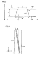
- Fig. 3 shows a schematic cross-sectional view of one example of the aperture array structure according to the present invention as shown in Fig. 2 , taken along a P-P' cross-section in Fig. 2 .
- the cross-sectional shape of the aperture is substantially a trapezoid.
- a hole size d1 of the aperture 11 at the first principal surface of the aperture array structure 1 (the upper side in Fig. 3 ) is smaller than a hole size d2 of the aperture 11 at the second principal surface (the lower side in the drawing). That is, the opening area of the aperture 11 at the first principal surface 10a1 of the aperture array structure 1 is smaller than the opening area of the same aperture 11 at the second principal surface 10a2 of the aperture array structure 1.
- the ratio (opening area ratio) of the opening area of the aperture at the second principal surface relative to the opening area of the aperture at the first principal surface is preferably 1.02 to 2.5. If the opening area ratio is increased, it is necessary to reduce the size of the opening in the first principal surface, and thus the transmittance of the entire aperture array structure for an electromagnetic wave is decreased. The decrease in transmittance leads to a decrease in measurement accuracy. Thus, in order to reduce a ratio of decrease in transmittance as a change amount to be about 10% or lower, it is necessary to make the opening area ratio to be not higher than 2.5. This relationship is obtained as follows.
- a maximum transmittance in a transmittance spectrum obtained when an electromagnetic wave is applied from a normal direction at the second principal surface side is defined as an initial value (100%)
- a relationship is analyzed between: the ratio (%), relative to the above initial value, of the similar maximum transmittance of the aperture array structure in which the hole size at the first principal surface is changed in a range of 1.3 to 1.8 ⁇ m and the hole size at the second principal surface is changed in a range of 1.8 to 2.3 ⁇ m; and the opening area ratio at that time.
- the opening area ratio is less than 1.02, improvement of the measurement sensitivity is slight (within an error range), and the advantageous effects of the present invention are not obtained.
- the opening of the aperture at the first principal surface has a size that does not allow a specimen to pass therethrough
- the opening of the aperture at the second principal surface has a size that allows a specimen to pass therethrough.
- the angle ⁇ formed between the first principal surface 10a1 of the aperture array structure 1 and an inner wall 11a of the aperture 11 is an acute angle.
- each aperture 11 of the aperture array structure 1 has such a shape, it is possible to increase localization of an electromagnetic field of the applied electromagnetic wave near a portion where the first principal surface 10a1 of the aperture array structure 1 and the inner wall 11a of the aperture 11 are in contact with each other.
- a change in frequency characteristics of a detected electromagnetic wave which change is caused by presence/absence of a specimen near the portion where the first principal surface of the aperture array structure and the inner wall of the aperture are in contact with each other becomes great, and thus it is possible to improve the measurement sensitivity. That is, even when the amount of a specimen is small, measurement is possible with high sensitivity.
- the inner wall 11a of the aperture 11 preferably has a recess.
- the inner wall 11a is preferably formed so as to draw a curved line that bulges outward of the aperture 11. Accordingly, it is made easier to collect a specimen within the aperture 11.
- the dimensions and the arrangement of the apertures of the aperture array structure, the thickness of the aperture array structure, and the like are not particularly limited, and are set as appropriate in accordance with a measurement method, the material characteristics of the aperture array structure, the frequency of an electromagnetic wave to be used, and the like.
- the hole size of each aperture which is indicated by d in Fig. 2(b) (the size of the opening at the side where the electromagnetic wave is applied) is preferably equal to or larger than one-tenth of the wave length of the electromagnetic wave used in measurement and equal to or smaller than 10 times that of this wave length.
- the hole size is preferably 0.15 to 150 ⁇ m, and in terms of improvement of the measurement sensitivity, the hole size is preferably 0.9 to 9 ⁇ m.
- the opening area of the aperture at the side where the electromagnetic wave is applied is preferably 0.0225 to 22500 ⁇ m 2 and more preferably 0.81 to 81 ⁇ m 2 .
- the grating space (pitch) between each aperture which is indicated by s in Fig. 2(b) is preferably equal to or smaller than one-tenth of the wave length of the electromagnetic wave used in measurement and equal to or larger than 10 times that of this wave length. By so setting, scattering more easily occurs.
- the grating space is preferably 0.15 to 150 ⁇ m, and in terms of improvement of the measurement sensitivity, the grating space is preferably 1.3 to 13 ⁇ m.
- the thickness of the aperture array structure is preferably equal to or smaller than 5 times that of the wave length of the electromagnetic wave used in measurement.
- An optimum wave length of an electromagnetic wave to be applied (a wave length at which high measurement sensitivity is ensured) is different depending on the dielectric constant or the shape of a specimen.
- the optimum wave length of the electromagnetic wave to be applied tends to be shorter as the thickness of the specimen is decreased. Accordingly, when the grating space and the opening area of each aperture at the side where the electromagnetic wave is applied are decreased, it is possible to ensure high measurement sensitivity.
- the optimum wave length of the electromagnetic wave to be applied tends to be shorter as the particle diameter of the specimen is decreased. Accordingly, when the grating space and the opening area of each aperture at the side where the electromagnetic wave is applied are decreased, it is possible to ensure high measurement sensitivity.
- the dimension of the entire aperture array structure is not particularly limited, and is determined in accordance with the area of a beam spot of the electromagnetic wave to be applied, or the like.
- At least a part of the surface of the aperture array structure is preferably formed of a conductor. At least a part of the surface of the aperture array structure 1 is a part of the surface of any one of a principal surface 10a, a side surface 10b, and the inner wall 11a of the aperture shown in Fig. 2(a) .
- the conductor refers to an object (substance) that conducts electricity, and not only a metal but also a semiconductor is included.
- the metal include a metal capable of bonding to a functional group of a compound having the functional group such as a hydroxy group, a thiol group, and a carboxyl group, a metal whose surface can be coated with a functional group such as a hydroxy group and an amino group, and an alloy of these metals.
- Specific examples thereof include gold, silver, copper, iron, nickel, chromium, silicon, germanium, and the like, and the metal is preferably gold, silver, copper, nickel, or chromium, and more preferably gold or nickel.
- the semiconductor examples include a compound semiconductor such as a group IV semiconductor (Si, Ge, and the like), a group II-VI semiconductor (ZnSe, CdS, ZnO, and the like), a group III-V semiconductor (GaAs, InP, GaN, and the like), a group IV compound semiconductor (SiC, SiGe, and the like), and a group I-III-VI semiconductor (CuInSe 2 and the like), and an organic semiconductor.
- a compound semiconductor such as a group IV semiconductor (Si, Ge, and the like), a group II-VI semiconductor (ZnSe, CdS, ZnO, and the like), a group III-V semiconductor (GaAs, InP, GaN, and the like), a group IV compound semiconductor (SiC, SiGe, and the like), and a group I-III-VI semiconductor (CuInSe 2 and the like), and an organic semiconductor.
- the specimen may be attached directly to the aperture array structure or may be attached thereto via a support film.
- the specimen is preferably attached directly to the surface of the aperture array structure.
- the cases where the specimen is attached directly to the aperture array structure include not only a case where a chemical bond or the like is directly formed between the surface of the aperture array structure and the specimen but also a case where the specimen is bound to a host molecule attached in advance to the surface of the aperture array structure.
- the chemical bond can include a covalent bond (e.g., a covalent bond between a metal and a thiol group) a Van der Waals bond, an ionic bond, a metallic bond, and a hydrogen bond.
- the chemical bond is the covalent bond.
- the host molecule is a molecule to which the specimen can be specifically bound.
- Examples of a combination of the host molecule and the specimen include an antigen and an antibody, a sugar chain and a protein, a lipid and a protein, a low-molecular compound (ligand) and a protein, a protein and a protein, and a single-stranded DNA and a single-stranded DNA.
- characteristics of the specimen are measured on the basis of at least one parameter relating to the frequency characteristics of the scattered electromagnetic wave in the aperture array structure obtained as described above.
- the characteristics of the specimen can be measured on the basis of a change in a dip waveform generated in the frequency characteristics of the electromagnetic wave forward-scattered (passing) through the aperture array structure 1 or a peak waveform generated in the frequency characteristics of the electromagnetic wave back-scattered (reflected) therefrom, the change being caused by the presence of the specimen.
- the dip waveform is a waveform in a valley portion (convex downward) that partially appears in the frequency characteristics (e.g., a transmittance spectrum) of the aperture array structure in a frequency range where the ratio of a detected electromagnetic wave relative to an electromagnetic wave applied (e.g., the transmittance of the electromagnetic wave) relatively increases.
- the peak waveform is a mountain shaped (upward convex) waveform that partially appears in the frequency characteristics (e.g., a reflectance spectrum) of the aperture array structure in a frequency range where the ratio of a detected electromagnetic wave relative to an electromagnetic wave applied (e.g., the reflectance of the electromagnetic wave) decreases.
- An aperture array structure having a square grating arrangement with square holes as shown in Fig. 2 was used as an aperture array structure.
- the grating space is 260 ⁇ m (s), and the thickness is 60 ⁇ m (t).
- the cross-sectional shape of each aperture in the P-P' cross-section in Fig. 2 is substantially a trapezoid.
- the hole size d1 at the first principal surface 10a1 side was 160 ⁇ m
- the hole size d2 at the second principal surface 10a2 side was 200 ⁇ m.
- a parallel plate sample (specimen) having a film thickness of 4 ⁇ m, a real part of a complex index of refraction of 1.55, and an imaginary part of the complex index of refraction of 0 was brought into close contact with the first principal surface 10a1 side of the aperture array structure 1, an electromagnetic wave was applied from the first principal surface 10a1 side (the arrow direction of a Z axis in Fig. 3 ), and a transmittance spectrum of the electromagnetic wave was calculated.
- the calculation was performed by using an electromagnetic field simulator (Microstripes: manufactured by CST) for a model (see Fig. 4 ) in which the aperture array structure 1 was provided between two ports 91 and 92 spaced apart from each other at an interval of 600 ⁇ m.
- Polarization of the electromagnetic wave to be applied to the aperture array structure 1 was linear polarization (parallel to a Y axis in Fig. 2 ), and the travelling direction thereof was the arrow direction of the Z axis.
- the aperture array structure 1 was positioned such that the principal surface thereof was perpendicular to the travelling direction of the electromagnetic wave (the Z axis direction) (i.e., such that ⁇ in Fig. 4 was 0 degree).
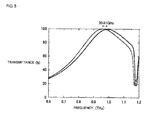
- Fig. 5 shows transmittance spectra obtained through the calculation.
- a solid line denotes a transmittance spectrum obtained when no specimen was held on the aperture array structure
- a broken line denotes a transmittance spectrum obtained when the specimen was held on the aperture array structure.
- the difference (frequency shift amount) between frequencies at which peaks appeared in the transmittance spectra was 30.81 GHz.
- the frequency shift amount in the case where each of d1 and d2 was 160 ⁇ m was 29.00 GHz
- the frequency shift amount in the case where each of d1 and d2 was 180 ⁇ m was 29.91 GHz
- the frequency shift amount in the case where each of d1 and d2 was 200 ⁇ m was 28.09 GHz.
- Example 1 and Comparative Example 1 From the results of Example 1 and Comparative Example 1, it is understood that since the opening area at the first principal surface and the opening area at the second principal surface of the aperture array structure were different from each other, the frequency shift amount increased and the measurement sensitivity improved. In addition, from the results of Example 1 and Comparative Example 1, it is understood that since the angle formed between the first principal surface of the aperture array structure and the inner wall of each aperture was an acute angle, the frequency shift amount increased and the measurement sensitivity improved.
Landscapes
- Physics & Mathematics (AREA)
- Spectroscopy & Molecular Physics (AREA)
- Health & Medical Sciences (AREA)
- General Physics & Mathematics (AREA)
- Analytical Chemistry (AREA)
- Chemical & Material Sciences (AREA)
- Life Sciences & Earth Sciences (AREA)
- Biochemistry (AREA)
- General Health & Medical Sciences (AREA)
- Immunology (AREA)
- Pathology (AREA)
- Toxicology (AREA)
- Optics & Photonics (AREA)
- Investigating Or Analysing Materials By Optical Means (AREA)
Abstract
Description
- The present invention relates to an aperture array structure used for measurement of a specimen and a measurement method using the same.
- Hitherto, a measurement method has been used in which to analyze characteristics of a substance, a specimen is held on an aperture array structure, an electromagnetic wave is applied to the aperture array structure on which the specimen has been held, and a transmission spectrum or the like thereof is analyzed to detect characteristics of the specimen. A specific example thereof is a method of applying a terahertz wave to a specimen, such as a protein, attached to a metal mesh, and analyzing a transmission spectrum thereof.
- As an existing technique which is such a method of analyzing a transmission spectrum using an electromagnetic wave, for example, Patent Document 1 (Japanese Unexamined Patent Application Publication No.
2007-010366 - In the aperture array structure disclosed in
Patent Document 1, from the description of Fig. 18(b) and the like, the opening area of each aperture at the front side is basically substantially the same as that at the back side, the angle formed between an inner wall surface forming each aperture and a principal surface of the aperture array structure is assumed as substantially 90 degrees. - In such a case, if the amount of a specimen is small, a change in frequency characteristics is slight, and detection is difficult. Thus, provision of a measurement device for realizing measurement with excellent measurement sensitivity is still desired.
- Patent Document 1: Japanese Unexamined Patent Application Publication No.
2007-010366 - It is an object of the present invention to provide an aperture array structure for realizing measurement with more excellent measurement sensitivity than that in the related art, and a measurement method using the same.
- The present invention is as follows.
- (1) An aperture array structure used in a method of measuring characteristics of a specimen by applying an electromagnetic wave to an aperture array structure on which the specimen is held, and detecting frequency characteristics of the electromagnetic wave scattered by the aperture array structure, the aperture array structure comprising: a first principal surface; a second principal surface opposed to the first principal surface; and a plurality of apertures extending through the aperture array structure in a direction perpendicular to the first principal surface and the second principal surface, wherein an opening area of each aperture at the first principal surface is smaller than an opening area of each aperture at the second principal surface.
- (2) The aperture array structure of the above (1), wherein an angle formed between the first principal surface of the aperture array structure and at least one inner wall of each aperture is an acute angle.
- (3) The aperture array structure of the above (1) or (2), wherein a ratio of the opening area of each aperture at the second principal surface relative to the opening area of each aperture at the first principal surface is 1.02 to 2.5.
- (4) The aperture array structure of any one of the above (1) to (3), wherein an opening of each aperture at the first principal surface has a size that does not allow the specimen to pass therethrough, and an opening of each aperture at the second principal surface has a size that allows the specimen to pass therethrough.
- (5) The aperture array structure of any one of the above (1) to (4), wherein an inner wall of each aperture has a recess.
- (6) A measurement method of measuring characteristics of a specimen by applying an electromagnetic wave to an aperture array structure on which the specimen is held, and detecting frequency characteristics of the electromagnetic wave scattered by the aperture array structure, the measurement method comprising using the aperture array structure of the above (1).
- (7) A measurement method of measuring characteristics of a specimen by applying an electromagnetic wave to an aperture array structure on which the specimen is held, and detecting frequency characteristics of the electromagnetic wave scattered by the aperture array structure, the measurement method comprising using the aperture array structure of the above (2) to hold the specimen near the first principal surface of the aperture array structure.
- (8) A measurement method of measuring characteristics of a specimen by applying an electromagnetic wave to an aperture array structure on which the specimen is held, and detecting frequency characteristics of the electromagnetic wave scattered by the aperture array structure, the measurement method comprising using the aperture array structure of the above (2) to hold the specimen near the second principal surface of the aperture array structure.
- (9) A measurement method comprising using the aperture array structure of the above (4) and moving the specimen from the second principal surface side of the aperture array structure in a direction to the first principal surface to hold the specimen at at least some of the apertures of the aperture array structure.
- The aperture array structure according to the present invention includes apertures each having an opening area at the first principal surface smaller than an opening area at the second principal surface. Thus, an electromagnetic field concentrates on the vicinity of a portion where the first principal surface of the aperture array structure and the inner wall of each aperture are in contact with each other. As a result, a change in frequency characteristics of the detected electromagnetic wave which change is caused by presence/absence of a specimen in the vicinity of the portion where the first principal surface of the aperture array structure and the inner wall of each aperture are in contact with each other increases, and thus measurement sensitivity improves.
-
- [
Fig. 1] Fig. 1 is a schematic diagram for explaining an outline of a measurement method according to the present invention. - [
Fig. 2] Fig. 2 is a schematic diagram for explaining a structure of an aperture array structure used in the present invention. - [
Fig. 3] Fig. 3 is a schematic cross-sectional view taken along a P-P' cross-section inFig. 2 . - [
Fig. 4] Fig. 4 is a schematic diagram showing an installed of an aperture array structure according to Example 1 is. - [
Fig. 5] Fig. 5 is a diagram showing a transmission spectrum obtained in Example 1. - First, an outline of one example of a measurement method according to the present invention will be described with reference to
Fig. 1. Fig. 1 is a diagram schematically showing the entire structure of one example of a measurement device used in the measurement method according to the present invention. The measurement device uses a pulse of an electromagnetic wave (e.g., a terahertz wave with a frequency of 20 GHz to 120 THz) generated by applying a laser beam from a laser 2 (e.g., a short pulse laser) to a semiconductor material. - In the configuration of
FIG. 1 , the laser beam emitted from thelaser 2 is branched into two paths by ahalf mirror 20. One of the branched laser beams is applied to aphotoconductive element 71 at the electromagnetic wave generation side, and the other laser beam is applied to aphotoconductive element 72 at the reception side via atime delay stage 26 by using a plurality of mirrors 21 (reference numerals are omitted for other mirrors having the same function). As each of thephotoconductive elements laser 2, a fiber laser or a laser using a solid such as titanium sapphire may be used. The electromagnetic wave may be generated and detected by using the surface of a semiconductor without an antenna, or by using an electro-optical crystal such as a ZnTe crystal. An appropriate bias voltage is applied from apower supply 3 to the gap portion of thephotoconductive element 71 at the generation side. - The generated electromagnetic wave is converted to a parallel beam by a
parabolic mirror 22 and is applied to anaperture array structure 1 by aparabolic mirror 23. The terahertz wave having passed through theaperture array structure 1 is received by thephotoconductive element 72 viaparabolic mirrors photoconductive element 72 is amplified by anamplifier 6 and then obtained as a time waveform in a lock-inamplifier 4. The obtained time waveform is subjected to signal processing, such as Fourier transform, in a PC (personal computer) 5 including calculation means, and then a transmittance spectrum of theaperture array structure 1 and the like are calculated. To obtain the time waveform in the lock-inamplifier 4, the bias voltage applied from thepower supply 3 to the gap of thephotoconductive element 71 at the generation side is modulated (with an amplitude of 5 V to 30 V) by using a signal from anoscillator 8. With synchronous detection using the modulated voltage, it is possible to increase a signal to noise ratio. - The above-described measurement method is a method generally called terahertz time-domain spectroscopy (THz-TDS). A Fourier transform infrared spectroscopy (FT-IR) may be used instead of the THz-TDS.
-
FIG. 1 shows a case where scattering is transmission, that is, a case of measuring a transmittance of the electromagnetic wave. In the present invention, "scattering" means a broad concept including transmission which is one mode of forward scattering, reflection which is one mode of backward scattering, and the like, and is preferably transmission or reflection. Further preferably, scattering is transmission in a zero-order direction or reflection in the zero-order direction. - In general, where s indicates the grating space of a diffraction grating, i indicates an incident angle, θ indicates a diffraction angle, and λ indicates a wave length, a spectrum diffracted by the diffraction grating can be represented as:

- The electromagnetic wave used in the present invention is not particularly limited as long as it is an electromagnetic wave capable of causing scattering in response to the structure of the aperture array structure. Any of a radio wave, an infrared ray, a visible ray, an ultraviolet ray, an X-ray, a gamma ray, and the like may be used, and the frequency thereof is also not particularly limited but is preferably 1 GHz to 1 PHz, and the electromagnetic wave is more preferably a terahertz wave having a frequency of 20 GHz to 200 THz.
- As the electromagnetic wave, a linearly polarized electromagnetic wave having a predetermined polarization direction (a linearly polarized wave) or an unpolarized electromagnetic wave (unpolarized wave) may be used. Examples of the linearly polarized electromagnetic wave include a terahertz wave generated by an optical rectification effect of an electrooptic crystal such as ZnTe with a short pulse laser as a light source, a visible ray emitted from a semiconductor laser, an electromagnetic wave radiated from a photoconductive antenna, and the like. Examples of the unpolarized electromagnetic wave include an infrared ray radiated from a high-pressure mercury lamp or a ceramic lamp, and the like.
- In the present invention, measurement of presence/absence or an amount of a specimen is quantification of a compound that is the specimen. Examples thereof include measurement of the content of a very small quantity of the specimen in a solution or the like and identification of the specimen.
- The aperture array structure according to the present invention has a first principal surface, a second principal surface opposed to the first principal surface, and a plurality of apertures extending therethrough in a direction perpendicular to the first principal surface and the second principal surface, and the opening area of each aperture on the first principal surface is smaller than the opening area of each aperture on the second principal surface.
- For example, the plurality of apertures are arranged periodically in at least one direction on the principal surface of the aperture array structure. However, all of the apertures may be periodically arranged, or some of the apertures may be periodically arranged and the other apertures may be non-periodically arranged as long as the advantageous effects of the present invention are not impaired.
- The aperture array structure is preferably a quasi-periodic structure or a periodic structure. The quasi-periodic structure is a structure that does not have translational symmetry but keeps order in array. Examples of the quasi-periodic structure include a Fibonacci structure as a one-dimensional quasi-periodic structure and a Penrose structure as a two-dimensional quasi-periodic structure. The periodic structure is a structure that has spatial symmetry, typified by translational symmetry, and is classified into a one-dimensional periodic structure, a two-dimensional periodic structure, and a three-dimensional periodic structure, depending on the dimension of the symmetry. Examples of the one-dimensional periodic structure include a wire-grid structure and a one-dimensional diffraction grating. Examples of the two-dimensional periodic structure include a mesh filter and a two-dimensional diffraction grating. Among these periodic structures, the two-dimensional periodic structure is preferably used.
- One example of the two-dimensional periodic structure is a plate-shaped structure (grating-shaped structure) shown in
Fig. 2 , in which apertures are arranged at constant intervals in a matrix. Theaperture array structure 1 shown inFig. 2(a) is a plate-shaped structure in which apertures each having a square shape as seen from theprincipal surface 10a side thereof are spaced at equal intervals in two arrangement directions perpendicular to the respective sides of the square (vertically and laterally in the drawing). - Then angle formed between the first principal surface of the aperture array structure and at least one inner wall of each aperture is preferably an acute angle. Here, "at least one inner wall" means one of the surfaces forming the inner walls of the aperture. Therefore, a portion where the first principal surface of the aperture array structure and the inner wall intersects each other may be sharp, or R (a curved surface) may be formed at this portion. If R is formed, breakage or the like of this portion is suppressed, and it is possible to improve the strength of the aperture array structure.
- The cross-sectional shape of each aperture on such a specific cross-section is not particularly limited, but examples thereof include a trapezoid and a shape that is generally a trapezoid. In other words, an example thereof is a shape in which the aperture widens from the first principal surface side (the side at which the opening area is small) toward the second principal surface side (the side at which the opening area is large) of the aperture array structure. The angle formed between the first principal surface of the aperture array structure and at least one inner wall of each aperture can be confirmed, for example, by observing a cross-section perpendicular to the principal surface of the aperture structure.
-
Fig. 3 shows a schematic cross-sectional view of one example of the aperture array structure according to the present invention as shown inFig. 2 , taken along a P-P' cross-section inFig. 2 . As shown inFig. 3 , the cross-sectional shape of the aperture is substantially a trapezoid. A hole size d1 of theaperture 11 at the first principal surface of the aperture array structure 1 (the upper side inFig. 3 ) is smaller than a hole size d2 of theaperture 11 at the second principal surface (the lower side in the drawing). That is, the opening area of theaperture 11 at the first principal surface 10a1 of theaperture array structure 1 is smaller than the opening area of thesame aperture 11 at the second principal surface 10a2 of theaperture array structure 1. - The ratio (opening area ratio) of the opening area of the aperture at the second principal surface relative to the opening area of the aperture at the first principal surface is preferably 1.02 to 2.5. If the opening area ratio is increased, it is necessary to reduce the size of the opening in the first principal surface, and thus the transmittance of the entire aperture array structure for an electromagnetic wave is decreased. The decrease in transmittance leads to a decrease in measurement accuracy. Thus, in order to reduce a ratio of decrease in transmittance as a change amount to be about 10% or lower, it is necessary to make the opening area ratio to be not higher than 2.5. This relationship is obtained as follows. For example, for an aperture array structure in which the hole size at the first principal surface is 1.8 µm and the hole size at the second principal surface is 1.8 µm (1:1 as a ratio), where a maximum transmittance in a transmittance spectrum obtained when an electromagnetic wave is applied from a normal direction at the second principal surface side is defined as an initial value (100%), a relationship is analyzed between: the ratio (%), relative to the above initial value, of the similar maximum transmittance of the aperture array structure in which the hole size at the first principal surface is changed in a range of 1.3 to 1.8 µm and the hole size at the second principal surface is changed in a range of 1.8 to 2.3 µm; and the opening area ratio at that time. In addition, if the opening area ratio is less than 1.02, improvement of the measurement sensitivity is slight (within an error range), and the advantageous effects of the present invention are not obtained.
- In addition, preferably, the opening of the aperture at the first principal surface has a size that does not allow a specimen to pass therethrough, and the opening of the aperture at the second principal surface has a size that allows a specimen to pass therethrough. In this case, when a specimen is moved (e.g., caused to flow) from the second principal surface side toward the first principal surface of the aperture array structure, the specimen is allowed to be held by at least a part of the apertures of the aperture array structure, and is allowed to be stably collected within the apertures and be measured.
- In a cross-section (P-P' cross-section) perpendicular to the first principal surface 10a1 of the
aperture array structure 1 shown inFig. 3 , the angle ψ formed between the first principal surface 10a1 of theaperture array structure 1 and aninner wall 11a of theaperture 11 is an acute angle. - In the case where each
aperture 11 of theaperture array structure 1 has such a shape, it is possible to increase localization of an electromagnetic field of the applied electromagnetic wave near a portion where the first principal surface 10a1 of theaperture array structure 1 and theinner wall 11a of theaperture 11 are in contact with each other. As a result, a change in frequency characteristics of a detected electromagnetic wave which change is caused by presence/absence of a specimen near the portion where the first principal surface of the aperture array structure and the inner wall of the aperture are in contact with each other becomes great, and thus it is possible to improve the measurement sensitivity. That is, even when the amount of a specimen is small, measurement is possible with high sensitivity. - It should be noted that when a specimen is held near the second principal surface having a large opening area, measurement is performed in a region where leak of an electromagnetic field is great, and thus another advantage is obtained that it is made possible to also measure a larger specimen.
- The
inner wall 11a of theaperture 11 preferably has a recess. In other words, theinner wall 11a is preferably formed so as to draw a curved line that bulges outward of theaperture 11. Accordingly, it is made easier to collect a specimen within theaperture 11. - The dimensions and the arrangement of the apertures of the aperture array structure, the thickness of the aperture array structure, and the like are not particularly limited, and are set as appropriate in accordance with a measurement method, the material characteristics of the aperture array structure, the frequency of an electromagnetic wave to be used, and the like.
- For example, in the
aperture array structure 1 in which the apertures are regularly arranged vertically and horizontally as shown inFig. 2(a) , the hole size of each aperture which is indicated by d inFig. 2(b) (the size of the opening at the side where the electromagnetic wave is applied) is preferably equal to or larger than one-tenth of the wave length of the electromagnetic wave used in measurement and equal to or smaller than 10 times that of this wave length. By so setting, the intensity of the electromagnetic wave scattered is increased, and it is made easier to detect a signal. Specifically, the hole size is preferably 0.15 to 150 µm, and in terms of improvement of the measurement sensitivity, the hole size is preferably 0.9 to 9 µm. - In addition, the opening area of the aperture at the side where the electromagnetic wave is applied is preferably 0.0225 to 22500 µm2 and more preferably 0.81 to 81 µm2.
- In addition, in the
aperture array structure 1 in which the apertures are regularly arranged vertically and horizontally as shown inFig. 2(a) , the grating space (pitch) between each aperture which is indicated by s inFig. 2(b) is preferably equal to or smaller than one-tenth of the wave length of the electromagnetic wave used in measurement and equal to or larger than 10 times that of this wave length. By so setting, scattering more easily occurs. Specifically, the grating space is preferably 0.15 to 150 µm, and in terms of improvement of the measurement sensitivity, the grating space is preferably 1.3 to 13 µm. - Moreover, the thickness of the aperture array structure is preferably equal to or smaller than 5 times that of the wave length of the electromagnetic wave used in measurement. By so setting, the intensity of the electromagnetic wave scattered is increased, and it is made easier to detect a signal.
- An optimum wave length of an electromagnetic wave to be applied (a wave length at which high measurement sensitivity is ensured) is different depending on the dielectric constant or the shape of a specimen. However, for example, when a specimen is a plate-shaped sample, in general, if the dielectric constant is the same, the optimum wave length of the electromagnetic wave to be applied tends to be shorter as the thickness of the specimen is decreased. Accordingly, when the grating space and the opening area of each aperture at the side where the electromagnetic wave is applied are decreased, it is possible to ensure high measurement sensitivity. In addition, for example, when the specimen is a particulate sample, in general, if the dielectric constant is the same, the optimum wave length of the electromagnetic wave to be applied tends to be shorter as the particle diameter of the specimen is decreased. Accordingly, when the grating space and the opening area of each aperture at the side where the electromagnetic wave is applied are decreased, it is possible to ensure high measurement sensitivity.
- The dimension of the entire aperture array structure is not particularly limited, and is determined in accordance with the area of a beam spot of the electromagnetic wave to be applied, or the like.
- At least a part of the surface of the aperture array structure is preferably formed of a conductor. At least a part of the surface of the
aperture array structure 1 is a part of the surface of any one of aprincipal surface 10a, aside surface 10b, and theinner wall 11a of the aperture shown inFig. 2(a) . - The conductor refers to an object (substance) that conducts electricity, and not only a metal but also a semiconductor is included. Examples of the metal include a metal capable of bonding to a functional group of a compound having the functional group such as a hydroxy group, a thiol group, and a carboxyl group, a metal whose surface can be coated with a functional group such as a hydroxy group and an amino group, and an alloy of these metals. Specific examples thereof include gold, silver, copper, iron, nickel, chromium, silicon, germanium, and the like, and the metal is preferably gold, silver, copper, nickel, or chromium, and more preferably gold or nickel. In the case where gold or nickel is used, particularly, in the case where a host molecule has a thiol group (-SH group), it is advantageous since the host molecule can be bonded to the surface of the aperture array structure by using the thiol group. In the case where nickel is used, particularly, in the case where a host molecule has an alkoxylane group, it is advantageous since the host molecule can be bonded to the surface of the aperture array structure by using the alkoxylane group. Examples of the semiconductor include a compound semiconductor such as a group IV semiconductor (Si, Ge, and the like), a group II-VI semiconductor (ZnSe, CdS, ZnO, and the like), a group III-V semiconductor (GaAs, InP, GaN, and the like), a group IV compound semiconductor (SiC, SiGe, and the like), and a group I-III-VI semiconductor (CuInSe2 and the like), and an organic semiconductor.
- In the present invention, various publicly known methods may be used as a method of holding a specimen on the aperture array structure. For example, the specimen may be attached directly to the aperture array structure or may be attached thereto via a support film. In terms of performing measurement with reproducibility enhanced by improving the measurement sensitivity and suppressing variations in measurement, the specimen is preferably attached directly to the surface of the aperture array structure.
- The cases where the specimen is attached directly to the aperture array structure include not only a case where a chemical bond or the like is directly formed between the surface of the aperture array structure and the specimen but also a case where the specimen is bound to a host molecule attached in advance to the surface of the aperture array structure. Examples of the chemical bond can include a covalent bond (e.g., a covalent bond between a metal and a thiol group) a Van der Waals bond, an ionic bond, a metallic bond, and a hydrogen bond. Preferably, the chemical bond is the covalent bond. The host molecule is a molecule to which the specimen can be specifically bound. Examples of a combination of the host molecule and the specimen include an antigen and an antibody, a sugar chain and a protein, a lipid and a protein, a low-molecular compound (ligand) and a protein, a protein and a protein, and a single-stranded DNA and a single-stranded DNA.
- In the measurement method according to the present invention, characteristics of the specimen are measured on the basis of at least one parameter relating to the frequency characteristics of the scattered electromagnetic wave in the aperture array structure obtained as described above. For example, the characteristics of the specimen can be measured on the basis of a change in a dip waveform generated in the frequency characteristics of the electromagnetic wave forward-scattered (passing) through the
aperture array structure 1 or a peak waveform generated in the frequency characteristics of the electromagnetic wave back-scattered (reflected) therefrom, the change being caused by the presence of the specimen. - The dip waveform is a waveform in a valley portion (convex downward) that partially appears in the frequency characteristics (e.g., a transmittance spectrum) of the aperture array structure in a frequency range where the ratio of a detected electromagnetic wave relative to an electromagnetic wave applied (e.g., the transmittance of the electromagnetic wave) relatively increases. The peak waveform is a mountain shaped (upward convex) waveform that partially appears in the frequency characteristics (e.g., a reflectance spectrum) of the aperture array structure in a frequency range where the ratio of a detected electromagnetic wave relative to an electromagnetic wave applied (e.g., the reflectance of the electromagnetic wave) decreases.
- The present invention will be described in further detail below by means of examples, but the present invention is not limited to them.
- An aperture array structure having a square grating arrangement with square holes as shown in
Fig. 2 was used as an aperture array structure. The grating space is 260 µm (s), and the thickness is 60 µm (t). In addition, regarding the shape of each aperture in the aperture array structure, as shown inFig. 3 , the cross-sectional shape of each aperture in the P-P' cross-section inFig. 2 is substantially a trapezoid. The hole size d1 at the first principal surface 10a1 side was 160 µm, and the hole size d2 at the second principal surface 10a2 side was 200 µm. - A parallel plate sample (specimen) having a film thickness of 4 µm, a real part of a complex index of refraction of 1.55, and an imaginary part of the complex index of refraction of 0 was brought into close contact with the first principal surface 10a1 side of the
aperture array structure 1, an electromagnetic wave was applied from the first principal surface 10a1 side (the arrow direction of a Z axis inFig. 3 ), and a transmittance spectrum of the electromagnetic wave was calculated. - The calculation was performed by using an electromagnetic field simulator (Microstripes: manufactured by CST) for a model (see
Fig. 4 ) in which theaperture array structure 1 was provided between twoports aperture array structure 1 was linear polarization (parallel to a Y axis inFig. 2 ), and the travelling direction thereof was the arrow direction of the Z axis. In addition, theaperture array structure 1 was positioned such that the principal surface thereof was perpendicular to the travelling direction of the electromagnetic wave (the Z axis direction) (i.e., such that θ inFig. 4 was 0 degree). -
Fig. 5 shows transmittance spectra obtained through the calculation. InFig. 5 , a solid line denotes a transmittance spectrum obtained when no specimen was held on the aperture array structure, and a broken line denotes a transmittance spectrum obtained when the specimen was held on the aperture array structure. InFig. 5 , the difference (frequency shift amount) between frequencies at which peaks appeared in the transmittance spectra was 30.81 GHz. - As Comparative Example 1, for a case where the hole size d1 at the first principal surface 10a1 side of the
aperture array structure 1 and the hole size d2 at the second principal surface 10a2 side of theaperture array structure 1 were the same (a case where d1 = d2: a case where a cross-sectional shape of each aperture was a rectangular), a transmittance spectrum was calculated by using an electromagnetic field simulator, similarly to Example 1. Transmittance spectra in the case where no specimen was held and the case where a specimen was held in three cases, namely, in the case where each of d1 and d2 was 160 µm, in the case where each of d1 and d2 was 180 µm, in the case where each of d1 and d2 was 200 µm were calculated, and frequency shift amounts thereamong were obtained. - As a result, the frequency shift amount in the case where each of d1 and d2 was 160 µm was 29.00 GHz, the frequency shift amount in the case where each of d1 and d2 was 180 µm was 29.91 GHz, and the frequency shift amount in the case where each of d1 and d2 was 200 µm was 28.09 GHz.
- From the results of Example 1 and Comparative Example 1, it is understood that since the opening area at the first principal surface and the opening area at the second principal surface of the aperture array structure were different from each other, the frequency shift amount increased and the measurement sensitivity improved. In addition, from the results of Example 1 and Comparative Example 1, it is understood that since the angle formed between the first principal surface of the aperture array structure and the inner wall of each aperture was an acute angle, the frequency shift amount increased and the measurement sensitivity improved.
- The embodiment and Example disclosed this time are illustrative in all points and should be considered as not restrictive. The scope of the present invention is shown not by the above description but by the scope of claims, and it is intended that all modifications within the meaning and scope equivalent to the scope of claims are included. Reference Signs List
-
- 1
- aperture array structure
- 10a
- principal surface
- 10a1
- first principal surface
- 10a2
- second principal surface
- 10b
- side surface
- 10c
- outer periphery
- 11
- aperture
- 11a
- inner wall
- 2
- laser
- 20
- half mirror
- 21
- mirror
- 22, 23, 24, 25
- parabolic mirror
- 26
- time delay stage
- 3
- power supply
- 4
- lock-in amplifier
- 5
- PC (personal computer)
- 6
- amplifier
- 71, 72
- photoconductive element
- 8
- oscillator
- 91, 92
- port
Claims (9)
- An aperture array structure used in a method of measuring characteristics of a specimen by applying an electromagnetic wave to an aperture array structure on which the specimen is held, and detecting frequency characteristics of the electromagnetic wave scattered by the aperture array structure, the aperture array structure comprising:a first principal surface;a second principal surface opposed to the first principal surface; anda plurality of apertures extending through the aperture array structure in a direction perpendicular to the first principal surface and the second principal surface, whereinan opening area of each aperture at the first principal surface is smaller than an opening area of each aperture at the second principal surface.
- The aperture array structure according to claim 1, wherein an angle formed between the first principal surface of the aperture array structure and at least one inner wall of each aperture is an acute angle.
- The aperture array structure according to claim 1 or 2, wherein a ratio of the opening area of each aperture at the second principal surface relative to the opening area of each aperture at the first principal surface is 1.02 to 2.5.
- The aperture array structure according to any one of claims 1 to 3, wherein an opening of each aperture at the first principal surface has a size that does not allow the specimen to pass therethrough, and an opening of each aperture at the second principal surface has a size that allows the specimen to pass therethrough.
- The aperture array structure according to any one of claims 1 to 4, wherein an inner wall of each aperture has a recess.
- A measurement method of measuring characteristics of a specimen by applying an electromagnetic wave to an aperture array structure on which the specimen is held, and detecting frequency characteristics of the electromagnetic wave scattered by the aperture array structure, the measurement method comprising:using the aperture array structure according to claim 1.
- A measurement method of measuring characteristics of a specimen by applying an electromagnetic wave to an aperture array structure on which the specimen is held, and detecting frequency characteristics of the electromagnetic wave scattered by the aperture array structure, the measurement method comprising:using the aperture array structure according to claim 2 to hold the specimen near the first principal surface of the aperture array structure.
- A measurement method of measuring characteristics of a specimen by applying an electromagnetic wave to an aperture array structure on which the specimen is held, and detecting frequency characteristics of the electromagnetic wave scattered by the aperture array structure, the measurement method comprising:using the aperture array structure according to claim 2 to hold the specimen near the second principal surface of the aperture array structure.
- A measurement method comprising:using the aperture array structure according to claim 4 and moving the specimen from the second principal surface side of the aperture array structure in a direction to the first principal surface to hold the specimen at at least some of the apertures of the aperture array structure.
Applications Claiming Priority (2)
| Application Number | Priority Date | Filing Date | Title |
|---|---|---|---|
| JP2012166962 | 2012-07-27 | ||
| PCT/JP2013/068235 WO2014017266A1 (en) | 2012-07-27 | 2013-07-03 | Void-arranged structure and measurement method using same |
Publications (2)
| Publication Number | Publication Date |
|---|---|
| EP2878943A1 true EP2878943A1 (en) | 2015-06-03 |
| EP2878943A4 EP2878943A4 (en) | 2016-07-20 |
Family
ID=49997082
Family Applications (1)
| Application Number | Title | Priority Date | Filing Date |
|---|---|---|---|
| EP13822692.3A Withdrawn EP2878943A4 (en) | 2012-07-27 | 2013-07-03 | Void-arranged structure and measurement method using same |
Country Status (6)
| Country | Link |
|---|---|
| US (1) | US9341561B2 (en) |
| EP (1) | EP2878943A4 (en) |
| JP (1) | JP5967201B2 (en) |
| KR (1) | KR101672980B1 (en) |
| CN (1) | CN104380083A (en) |
| WO (1) | WO2014017266A1 (en) |
Families Citing this family (4)
| Publication number | Priority date | Publication date | Assignee | Title |
|---|---|---|---|---|
| CN205175893U (en) * | 2013-03-22 | 2016-04-20 | 株式会社村田制作所 | Tectosome for detection |
| JP5991426B2 (en) * | 2013-03-25 | 2016-09-14 | 株式会社村田製作所 | Void arrangement structure and measurement method using the same |
| CN113008907B (en) * | 2019-12-19 | 2024-04-12 | 华为技术有限公司 | Terahertz sensing system and terahertz sensing array |
| US11888233B2 (en) * | 2020-04-07 | 2024-01-30 | Ramot At Tel-Aviv University Ltd | Tailored terahertz radiation |
Family Cites Families (10)
| Publication number | Priority date | Publication date | Assignee | Title |
|---|---|---|---|---|
| US3980180A (en) * | 1974-11-20 | 1976-09-14 | Jamieson John A | Transmissive article sorting apparatus |
| JP4200795B2 (en) * | 2003-03-19 | 2008-12-24 | 日本電気株式会社 | Optical element, optical head, and optical recording / reproducing apparatus |
| JP4020142B2 (en) * | 2003-06-05 | 2007-12-12 | 株式会社村田製作所 | Manufacturing method of three-dimensional periodic structure |
| JP4724822B2 (en) | 2005-06-28 | 2011-07-13 | 株式会社アドバンテスト | Integrated structure, measuring apparatus, method and program |
| JP4822262B2 (en) * | 2006-01-23 | 2011-11-24 | 沖電気工業株式会社 | Circular waveguide antenna and circular waveguide array antenna |
| JP2008185552A (en) * | 2007-01-31 | 2008-08-14 | Tohoku Univ | Measuring apparatus and measuring method |
| JPWO2011013452A1 (en) * | 2009-07-29 | 2013-01-07 | 株式会社村田製作所 | Method, measuring device and filter device for measuring characteristics of object to be measured |
| JP5516589B2 (en) * | 2009-09-03 | 2014-06-11 | 株式会社村田製作所 | Method for measuring characteristic of object to be measured, and measurement system |
| US8865078B2 (en) * | 2010-06-11 | 2014-10-21 | Industrial Technology Research Institute | Apparatus for single-molecule detection |
| CN102401917A (en) * | 2011-11-16 | 2012-04-04 | 电子科技大学 | Middle-infrared waveband transmission type sub-wavelength metal grating |
-
2013
- 2013-07-03 WO PCT/JP2013/068235 patent/WO2014017266A1/en not_active Ceased
- 2013-07-03 KR KR1020157001439A patent/KR101672980B1/en active Active
- 2013-07-03 JP JP2014526837A patent/JP5967201B2/en active Active
- 2013-07-03 EP EP13822692.3A patent/EP2878943A4/en not_active Withdrawn
- 2013-07-03 CN CN201380032034.2A patent/CN104380083A/en active Pending
-
2015
- 2015-01-26 US US14/604,892 patent/US9341561B2/en active Active
Also Published As
| Publication number | Publication date |
|---|---|
| US9341561B2 (en) | 2016-05-17 |
| CN104380083A (en) | 2015-02-25 |
| KR20150023814A (en) | 2015-03-05 |
| US20150136989A1 (en) | 2015-05-21 |
| WO2014017266A1 (en) | 2014-01-30 |
| KR101672980B1 (en) | 2016-11-04 |
| JP5967201B2 (en) | 2016-08-10 |
| EP2878943A4 (en) | 2016-07-20 |
| JPWO2014017266A1 (en) | 2016-07-07 |
Similar Documents
| Publication | Publication Date | Title |
|---|---|---|
| JP5761416B2 (en) | Flat periodic structure | |
| US20160054223A1 (en) | Method for measuring analyte | |
| US8610071B2 (en) | Method of measuring characteristics of specimen, and flat-plate periodic structure | |
| US20150129769A1 (en) | Measurement Method for Object to be Measured | |
| US9341561B2 (en) | Aperture array structure and measurement method using the same | |
| US10408750B2 (en) | Void-arranged structure and measurement method using the same | |
| CN103562707B (en) | Measuring method of the measured object | |
| US9075006B2 (en) | Measurement device and feature measurement method of object to be measured employing same | |
| US20120126123A1 (en) | Method of Measuring Characteristics of Specimen, Measuring Device, and Filter Device | |
| US20130062524A1 (en) | Method of measuring characteristics of specimen, and aperture array structure and measuring device used in same | |
| US8912497B2 (en) | Measurement structure, method of manufacturing same, and measuring method using same | |
| JP5609654B2 (en) | Measuring method of measured object | |
| US9007578B2 (en) | Method for measurement of properties of analyte | |
| JP5983883B2 (en) | Measuring method of measured object | |
| JP2015017941A (en) | Measuring method and measuring apparatus of measuring object |
Legal Events
| Date | Code | Title | Description |
|---|---|---|---|
| PUAI | Public reference made under article 153(3) epc to a published international application that has entered the european phase |
Free format text: ORIGINAL CODE: 0009012 |
|
| 17P | Request for examination filed |
Effective date: 20141114 |
|
| AK | Designated contracting states |
Kind code of ref document: A1 Designated state(s): AL AT BE BG CH CY CZ DE DK EE ES FI FR GB GR HR HU IE IS IT LI LT LU LV MC MK MT NL NO PL PT RO RS SE SI SK SM TR |
|
| AX | Request for extension of the european patent |
Extension state: BA ME |
|
| DAX | Request for extension of the european patent (deleted) | ||
| RA4 | Supplementary search report drawn up and despatched (corrected) |
Effective date: 20160617 |
|
| RIC1 | Information provided on ipc code assigned before grant |
Ipc: G01N 21/3586 20140101AFI20160613BHEP Ipc: G02B 5/00 20060101ALI20160613BHEP |
|
| STAA | Information on the status of an ep patent application or granted ep patent |
Free format text: STATUS: THE APPLICATION IS DEEMED TO BE WITHDRAWN |
|
| 18D | Application deemed to be withdrawn |
Effective date: 20170117 |