EP2876794A1 - Input EMI filter and method for motor drive including an active rectifier - Google Patents
Input EMI filter and method for motor drive including an active rectifier Download PDFInfo
- Publication number
- EP2876794A1 EP2876794A1 EP14193689.8A EP14193689A EP2876794A1 EP 2876794 A1 EP2876794 A1 EP 2876794A1 EP 14193689 A EP14193689 A EP 14193689A EP 2876794 A1 EP2876794 A1 EP 2876794A1
- Authority
- EP
- European Patent Office
- Prior art keywords
- poly
- filter
- phase
- motor drive
- common mode
- Prior art date
- Legal status (The legal status is an assumption and is not a legal conclusion. Google has not performed a legal analysis and makes no representation as to the accuracy of the status listed.)
- Granted
Links
Images

Classifications
-
- H—ELECTRICITY
- H02—GENERATION; CONVERSION OR DISTRIBUTION OF ELECTRIC POWER
- H02P—CONTROL OR REGULATION OF ELECTRIC MOTORS, ELECTRIC GENERATORS OR DYNAMO-ELECTRIC CONVERTERS; CONTROLLING TRANSFORMERS, REACTORS OR CHOKE COILS
- H02P29/00—Arrangements for regulating or controlling electric motors, appropriate for both AC and DC motors
- H02P29/50—Reduction of harmonics
-
- H—ELECTRICITY
- H04—ELECTRIC COMMUNICATION TECHNIQUE
- H04B—TRANSMISSION
- H04B3/00—Line transmission systems
- H04B3/02—Details
- H04B3/28—Reducing interference caused by currents induced in cable sheathing or armouring
-
- H—ELECTRICITY
- H02—GENERATION; CONVERSION OR DISTRIBUTION OF ELECTRIC POWER
- H02M—APPARATUS FOR CONVERSION BETWEEN AC AND AC, BETWEEN AC AND DC, OR BETWEEN DC AND DC, AND FOR USE WITH MAINS OR SIMILAR POWER SUPPLY SYSTEMS; CONVERSION OF DC OR AC INPUT POWER INTO SURGE OUTPUT POWER; CONTROL OR REGULATION THEREOF
- H02M1/00—Details of apparatus for conversion
- H02M1/12—Arrangements for reducing harmonics from AC input or output
-
- H—ELECTRICITY
- H02—GENERATION; CONVERSION OR DISTRIBUTION OF ELECTRIC POWER
- H02M—APPARATUS FOR CONVERSION BETWEEN AC AND AC, BETWEEN AC AND DC, OR BETWEEN DC AND DC, AND FOR USE WITH MAINS OR SIMILAR POWER SUPPLY SYSTEMS; CONVERSION OF DC OR AC INPUT POWER INTO SURGE OUTPUT POWER; CONTROL OR REGULATION THEREOF
- H02M1/00—Details of apparatus for conversion
- H02M1/44—Circuits or arrangements for compensating for electromagnetic interference in converters or inverters
-
- H—ELECTRICITY
- H04—ELECTRIC COMMUNICATION TECHNIQUE
- H04B—TRANSMISSION
- H04B3/00—Line transmission systems
- H04B3/02—Details
- H04B3/30—Reducing interference caused by unbalanced currents in a normally balanced line
-
- G—PHYSICS
- G01—MEASURING; TESTING
- G01R—MEASURING ELECTRIC VARIABLES; MEASURING MAGNETIC VARIABLES
- G01R19/00—Arrangements for measuring currents or voltages or for indicating presence or sign thereof
- G01R19/25—Arrangements for measuring currents or voltages or for indicating presence or sign thereof using digital measurement techniques
- G01R19/2506—Arrangements for conditioning or analysing measured signals, e.g. for indicating peak values ; Details concerning sampling, digitizing or waveform capturing
- G01R19/2509—Details concerning sampling, digitizing or waveform capturing
-
- G—PHYSICS
- G01—MEASURING; TESTING
- G01R—MEASURING ELECTRIC VARIABLES; MEASURING MAGNETIC VARIABLES
- G01R19/00—Arrangements for measuring currents or voltages or for indicating presence or sign thereof
- G01R19/25—Arrangements for measuring currents or voltages or for indicating presence or sign thereof using digital measurement techniques
- G01R19/2513—Arrangements for monitoring electric power systems, e.g. power lines or loads; Logging
-
- G—PHYSICS
- G01—MEASURING; TESTING
- G01R—MEASURING ELECTRIC VARIABLES; MEASURING MAGNETIC VARIABLES
- G01R31/00—Arrangements for testing electric properties; Arrangements for locating electric faults; Arrangements for electrical testing characterised by what is being tested not provided for elsewhere
- G01R31/005—Testing of electric installations on transport means
- G01R31/006—Testing of electric installations on transport means on road vehicles, e.g. automobiles or trucks
- G01R31/007—Testing of electric installations on transport means on road vehicles, e.g. automobiles or trucks using microprocessors or computers
-
- H—ELECTRICITY
- H02—GENERATION; CONVERSION OR DISTRIBUTION OF ELECTRIC POWER
- H02M—APPARATUS FOR CONVERSION BETWEEN AC AND AC, BETWEEN AC AND DC, OR BETWEEN DC AND DC, AND FOR USE WITH MAINS OR SIMILAR POWER SUPPLY SYSTEMS; CONVERSION OF DC OR AC INPUT POWER INTO SURGE OUTPUT POWER; CONTROL OR REGULATION THEREOF
- H02M1/00—Details of apparatus for conversion
- H02M1/12—Arrangements for reducing harmonics from AC input or output
- H02M1/123—Suppression of common mode voltage or current
-
- H—ELECTRICITY
- H04—ELECTRIC COMMUNICATION TECHNIQUE
- H04B—TRANSMISSION
- H04B2203/00—Indexing scheme relating to line transmission systems
- H04B2203/54—Aspects of powerline communications not already covered by H04B3/54 and its subgroups
- H04B2203/5462—Systems for power line communications
- H04B2203/5475—Systems for power line communications adapted for drill or well combined with data transmission
Definitions
- the present invention relates generally to motor drives including active rectifiers, and more specifically to a motor drive including an input electromagnetic interference (EMI) filter.
- EMI electromagnetic interference
- Electric engine start systems utilize a motor drive (a switching-mode power conversion system) to control a motor/starter and employ an active rectifier as a front-end power converter to interface with a power supply.
- the active rectifier draws near sinusoidal currents from the power supply to meet specification requirements on input current harmonics.
- Both the active rectifier and the motor drive inverter employ fast switching IGBT devices controlled using a pulse-width modulation (PWM) technique.
- PWM pulse-width modulation
- the high frequency voltage components of PWM converter (the active rectifier) and inverter cause high frequency leakage currents and conducted EMI in the power lines and ground system.
- the conducted EMI can be classified into two-types: common-mode (CM) and differential-mode (DM) according to their circulation paths.
- CM noise The noise flowing within the power-feeding paths
- CM noise the noise flowing between the power conversion system and the ground
- CM noise the noise flowing between the power conversion system and the ground
- CM noise Typical EMI filters consist of an input section connected between the active rectifier and the power source, and an output section connected between the drive inverter and the motor. Both sections include DM and CM inductors, capacitors and resistors.
- the output section reduces high-frequency leakage currents due to parasitic motor winding capacitances to ground, as well as bearing currents, and shaft voltage.
- the radiated emissions are controlled by shielding drive inverter power lines to the motor.
- the motor drive inverter operates at higher output current in comparison to the active rectifier input current that results in a larger weight of EMI filter output section.
- some systems that operate a motor drive (i.e. engine start) at low duty cycle and utilize shielded output cable to the motor have implemented additional common mode filtering in the EMI filter input section to address additional CM noise contributed by the motor windings capacitive coupling to the ground.
- common mode filters do not use an increased total capacitance to ground for filtering. Instead, common mode filters use an increased inductance of at least one common mode choke in a multi-stage common mode filter in order to increase the insertion loss of the common mode filter. This construction makes the common mode filter bulky.
- a poly-phase motor drive including: an input EMI filter having a poly-phase filter input and a poly-phase filter output, an active rectifier connected to the filter output, the active rectifier having a DC output, and a motor drive inverter connected to the DC output, the motor drive inverter having a poly-phase motor control output.
- Also disclosed is a method for filtering a poly-phase motor drive including: filtering common mode noise from the switching-mode power conversion system, and filtering differential mode noise from the switching-mode power conversion system.
- the motor current of the motor drive (the output of the motor drive) is typically higher than the input line current (the input to the active rectifier).
- An EMI filter at the output of the motor drive must be sized to accommodate the increased motor current resulting in a large physical size of the common mode filter.
- the higher current requirement of the motor drive inverter requires a lower switching frequency in order to reduce inverter switching losses and improve the thermal performance of the inverter.
- the lower switching frequency and higher current characteristics of the motor drive inverter lead to an increased size requirement for an output EMI filter.
- FIG. 1 schematically illustrates a motor drive 10 including an active rectifier 40 and a motor drive inverter 50 that addresses the above increased size and weight requirements by incrementally increasing an input EMI filter 30 at the active rectifier 40 input and eliminating EMI filtering at the motor drive inverter 50 output.
- a three phase power source 20 provides electrical power to the motor drive 10. The current from the three phase power source 20 is passed through the input EMI filter 30 to the active rectifier 40.
- the active rectifier 40 comprises a conventional six-switch voltage source PWM converter and a three-phase boost inductor. In one example, the active rectifier 40 converts a three-phase AC input power into 750 volts DC output power at DC link 42.
- the switching-mode active rectifier 40 generates high frequency (HF) voltage components that cause HF leakage currents and conducted electromagnetic interference (EMI) noise which flows within power-feeding paths, and between the power conversion system and the ground.
- HF high frequency
- EMI conducted electromagnetic interference
- the DC link 42 is connected to an input of the motor drive inverter 50.
- the motor drive inverter 50 converts the received DC input power into a three phase AC output power on lines 52 to power the motor 70.
- the motor drive inverter 50 includes a conventional six-switch voltage source PWM inverter.
- the switching-mode inverter generates high frequency (HF) voltage components that cause HF leakage currents and conducted electromagnetic interference (EMI) noise which flows within power-feeding paths, and between the power conversion system and the ground.
- HF high frequency
- EMI conducted electromagnetic interference
- the switching frequency of the active rectifier 40 and the motor drive inverter 50 are the same and introduce the same frequency of common mode noise into the system.
- the switching frequencies are different (i.e. the inverter 50 switching frequency may be lower in comparison to the active rectifier 40 switching frequency in order to reduce inverter switching losses when operating the inverter 50 at higher output current levels), and introduce different frequencies of common mode noise into the system.
- the DC link 42 includes two DC link mid-point capacitors 44 connecting the terminals of the DC link 42.
- a bulk capacitor 46 is arranged in parallel to the two DC link mid-point capacitors 44.
- a floating point connection 60 connects the input EMI filter 30 to the DC link mid-point capacitors 44.
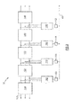
- FIG 2 illustrates a first example input EMI filter 30 that can be used in the motor drive 10 of Figure 1 .
- the input EMI filter 30 includes three phase inputs 103 that connect the three phase power source 20 (illustrated in Figure 1 ) to a high frequency CM choke 110.
- the high frequency CM choke 110 utilizes a feed-through ferrite toroid and filters out high frequency common mode noise originating from the switching-mode motor drive system 10.
- the output of the high frequency CM choke 110 is connected to a differential mode noise filter 120 and a first notch filter 160.
- the differential mode noise filter 120 uses a differential mode inductor on each phase to filter out differential mode noise originating from the switching-mode motor drive system 10.
- the first notch filter 160 includes an inductor in series with a capacitor on each phase. The notch filter arrangement filters out noise at the particular switching frequency to which the notch filter 160 is turned.
- the output of the first notch filter 160 is connected to the floating point connection 60 via an impedance block 108.
- the output of the differential mode noise filter 120 is connected to a first common mode choke 130 that utilizes a three-phase common mode inductor. Also connected to the output of the differential mode noise filter 120 is a second notch filter 170. As with the first notch filter 160, the second notch filter 170 includes an inductor in series with a capacitor on each phase and filters out noise at the particular switching frequency to which the second notch filter 170 is turned. The second notch filter 170 is connected to the floating point connection 60 via an impedance block 106.
- the output of the first common mode choke 130 is connected to a second common mode choke 140.
- the second common mode choke 140 includes a three-phase common mode inductor.
- the core material of the common mode inductors of the first common mode choke 130 and the core material of the common mode inductors of the second common mode choke 140 are different core materials.
- the core material of the common mode inductors in one of the common mode chokes 130, 140 is a ferrite material
- the core material in the other of the common mode chokes 130, 140 is a nano-crystalline materials.
- the common mode capacitor 180 includes a capacitor on each phase and provides additional filtering.
- the three phases of the common mode capacitor 180 are tied together and connected to the floating point connection 60 via an impedance block 104.
- the boost inductor 150 is part of the active rectifier 40 and includes at least one inductor on each phase of the active rectifier 40. Also connected between the boost inductor 150 and the second CM choke 140 is a differential mode (DM) capacitor/resistor 190 that includes a series connected capacitor and a damping resistor per phase.
- the boost inductor 150, DM capacitor 190, DM inductor 120, and the first notch filter 160 are a differential mode filter that reduces active rectifier differential mode noise and improves input current harmonic distortions.
- the first notch filter 160 is tuned to reject current components associated with active rectifier 40 switching frequency.
- the differential mode capacitor/resistor 190 is connected to the floating point connection 60 via an impedance block 102.
- the arrangement of the differential mode inductor 120, the boost inductor 150, and the differential mode capacitor 190 is referred to as a T-type differential mode filter.
- Each of the differential mode inductor 120, the boost inductor 150, and the differential mode capacitor 190 operate in conjunction to provide differential mode filtering of the input to the active rectifier 40.
- the common mode elements 110, 130, 140, and 180 operate in conjunction with each other to filter common mode noise.
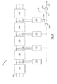
- Figure 3 illustrates an alternate arrangement for the input EMI filter 30 of Figure 1 .
- the alternate arrangement varies from the arrangement of Figure 2 in that the first and second common mode chokes 130, 140 and the common mode capacitor filter 180 are connected to a single impedance block 202 and the single impedance block 202 connects to the floating point connection 60.
- the differential mode capacitor/resistor 190 is connected to the floating point connection 60 via an impedance block 204, and the floating point connection 60 is connected to a neutral 208 via an impedance block 206.
- the floating point connection 60 is connected to the DC link 42 mid-point as illustrated in Figure 1 .
- the impedance blocks 102, 104, 106, 108, 202, 204, 206 are resistive/capacitive (RC) elements.
- the specific resistances and capacitances of the impedance blocks 102, 104, 106, 108, 202, 204, 206 depend on the needs of the specific system to divert common mode current into DC bus, and can be determined by one of skill in the art having the benefit of this disclosure.
- the active rectifier 40 and the motor drive inverter 50 each operate at a given switching frequency emitting EMI noise associated with these switching frequencies.
- the active rectifier 40 operates at 11 kHz and the motor drive inverter 50 operates at 8 kHz.
- additional EMI noise will be injected into the system at both 8 kHz and 11 kHz.
- Each of the notch filters 160, 170 are tuned to one of the switching frequencies to filter out the EMI noise in that particular frequency.
- both notch filters 160, 170 can be tuned to the same frequency, or one of the notch filters 160, 170 can be omitted entirely. While the notch filters 160, 170 are described herein as a "first notch filter 160" and a “second notch filter 170” it is understood that in a practical implementation the notch filters 160, 170 are interchangeable and either notch filter 160, 170 can be tuned to either switching frequency.
- motor drive 10 is described and illustrated with regards to a three phase motor drive input filter arrangement, one of skill in the art having the benefit of this disclosure will recognize that the motor drive input filter can be adapted to any poly-phase motor drive and still fall within the above disclosure.
Landscapes
- Engineering & Computer Science (AREA)
- Power Engineering (AREA)
- Computer Networks & Wireless Communication (AREA)
- Signal Processing (AREA)
- Physics & Mathematics (AREA)
- Electromagnetism (AREA)
- Inverter Devices (AREA)
Abstract
Description
- The present invention relates generally to motor drives including active rectifiers, and more specifically to a motor drive including an input electromagnetic interference (EMI) filter.
- Electric engine start systems utilize a motor drive (a switching-mode power conversion system) to control a motor/starter and employ an active rectifier as a front-end power converter to interface with a power supply. The active rectifier draws near sinusoidal currents from the power supply to meet specification requirements on input current harmonics. Both the active rectifier and the motor drive inverter employ fast switching IGBT devices controlled using a pulse-width modulation (PWM) technique. The high frequency voltage components of PWM converter (the active rectifier) and inverter cause high frequency leakage currents and conducted EMI in the power lines and ground system.
- The conducted EMI can be classified into two-types: common-mode (CM) and differential-mode (DM) according to their circulation paths. The noise flowing within the power-feeding paths is called DM noise, and the noise flowing between the power conversion system and the ground is called CM noise. Typical EMI filters consist of an input section connected between the active rectifier and the power source, and an output section connected between the drive inverter and the motor. Both sections include DM and CM inductors, capacitors and resistors. The output section reduces high-frequency leakage currents due to parasitic motor winding capacitances to ground, as well as bearing currents, and shaft voltage. The radiated emissions are controlled by shielding drive inverter power lines to the motor.
- In some systems the motor drive inverter operates at higher output current in comparison to the active rectifier input current that results in a larger weight of EMI filter output section. As an alternative to the excessive weight of EMI filter output section, some systems that operate a motor drive (i.e. engine start) at low duty cycle and utilize shielded output cable to the motor have implemented additional common mode filtering in the EMI filter input section to address additional CM noise contributed by the motor windings capacitive coupling to the ground.
- For safety reasons common mode filters do not use an increased total capacitance to ground for filtering. Instead, common mode filters use an increased inductance of at least one common mode choke in a multi-stage common mode filter in order to increase the insertion loss of the common mode filter. This construction makes the common mode filter bulky.
- Disclosed is a poly-phase motor drive including: an input EMI filter having a poly-phase filter input and a poly-phase filter output, an active rectifier connected to the filter output, the active rectifier having a DC output, and a motor drive inverter connected to the DC output, the motor drive inverter having a poly-phase motor control output.
- Also disclosed is a method for filtering a poly-phase motor drive including: filtering common mode noise from the switching-mode power conversion system, and filtering differential mode noise from the switching-mode power conversion system.
- These and other features of the present invention can be best understood from the following specification and drawings, the following of which is a brief description.
-
-
Figure 1 schematically illustrates a motor drive system including an active rectifier. -
Figure 2 schematically illustrates an example input EMI filter for a motor drive system. -
Figure 3 schematically illustrates an alternate example input EMI filter for a motor drive system. - In existing motor drives, the motor current of the motor drive (the output of the motor drive) is typically higher than the input line current (the input to the active rectifier). An EMI filter at the output of the motor drive must be sized to accommodate the increased motor current resulting in a large physical size of the common mode filter. The higher current requirement of the motor drive inverter requires a lower switching frequency in order to reduce inverter switching losses and improve the thermal performance of the inverter. The lower switching frequency and higher current characteristics of the motor drive inverter lead to an increased size requirement for an output EMI filter.
-
Figure 1 schematically illustrates amotor drive 10 including anactive rectifier 40 and amotor drive inverter 50 that addresses the above increased size and weight requirements by incrementally increasing aninput EMI filter 30 at theactive rectifier 40 input and eliminating EMI filtering at themotor drive inverter 50 output. A threephase power source 20 provides electrical power to themotor drive 10. The current from the threephase power source 20 is passed through theinput EMI filter 30 to theactive rectifier 40. Theactive rectifier 40 comprises a conventional six-switch voltage source PWM converter and a three-phase boost inductor. In one example, theactive rectifier 40 converts a three-phase AC input power into 750 volts DC output power atDC link 42. The switching-modeactive rectifier 40 generates high frequency (HF) voltage components that cause HF leakage currents and conducted electromagnetic interference (EMI) noise which flows within power-feeding paths, and between the power conversion system and the ground. - The
DC link 42 is connected to an input of themotor drive inverter 50. The motor drive inverter 50, in turn, converts the received DC input power into a three phase AC output power onlines 52 to power the motor 70. Themotor drive inverter 50 includes a conventional six-switch voltage source PWM inverter. The switching-mode inverter generates high frequency (HF) voltage components that cause HF leakage currents and conducted electromagnetic interference (EMI) noise which flows within power-feeding paths, and between the power conversion system and the ground. Due to the low-duty cycle utilization of the motor drive system for engine start applications, concerns related to the bearing currents and shaft voltage are reduced, while the common-mode noise associated with the high-frequency leakage currents due to motor windings capacitive coupling to the ground are addressed by incrementally increasing size of the input EMI filter. - In some examples, the switching frequency of the
active rectifier 40 and themotor drive inverter 50 are the same and introduce the same frequency of common mode noise into the system. In alternate examples, the switching frequencies are different (i.e. theinverter 50 switching frequency may be lower in comparison to theactive rectifier 40 switching frequency in order to reduce inverter switching losses when operating theinverter 50 at higher output current levels), and introduce different frequencies of common mode noise into the system. - In the example of
Figure 1 , theDC link 42 includes two DClink mid-point capacitors 44 connecting the terminals of theDC link 42. Abulk capacitor 46 is arranged in parallel to the two DClink mid-point capacitors 44. Afloating point connection 60 connects theinput EMI filter 30 to the DClink mid-point capacitors 44. -
Figure 2 illustrates a first exampleinput EMI filter 30 that can be used in themotor drive 10 ofFigure 1 . Theinput EMI filter 30 includes threephase inputs 103 that connect the three phase power source 20 (illustrated inFigure 1 ) to a highfrequency CM choke 110. The highfrequency CM choke 110 utilizes a feed-through ferrite toroid and filters out high frequency common mode noise originating from the switching-modemotor drive system 10. - The output of the high
frequency CM choke 110 is connected to a differentialmode noise filter 120 and afirst notch filter 160. The differentialmode noise filter 120 uses a differential mode inductor on each phase to filter out differential mode noise originating from the switching-modemotor drive system 10. Thefirst notch filter 160 includes an inductor in series with a capacitor on each phase. The notch filter arrangement filters out noise at the particular switching frequency to which thenotch filter 160 is turned. The output of thefirst notch filter 160 is connected to thefloating point connection 60 via animpedance block 108. - The output of the differential
mode noise filter 120 is connected to a firstcommon mode choke 130 that utilizes a three-phase common mode inductor. Also connected to the output of the differentialmode noise filter 120 is asecond notch filter 170. As with thefirst notch filter 160, thesecond notch filter 170 includes an inductor in series with a capacitor on each phase and filters out noise at the particular switching frequency to which thesecond notch filter 170 is turned. Thesecond notch filter 170 is connected to thefloating point connection 60 via animpedance block 106. - The output of the first
common mode choke 130 is connected to a secondcommon mode choke 140. As with the first common mode choke 130, the secondcommon mode choke 140 includes a three-phase common mode inductor. In some example embodiments, the core material of the common mode inductors of the first common mode choke 130 and the core material of the common mode inductors of the secondcommon mode choke 140 are different core materials. In further examples, the core material of the common mode inductors in one of thecommon mode chokes common mode chokes common mode chokes input EMI filter 30 to realize benefits of each type of common mode inductor simultaneously. - Also connected to the output of the second
common mode choke 130 is acommon mode capacitor 180. Thecommon mode capacitor 180 includes a capacitor on each phase and provides additional filtering. The three phases of thecommon mode capacitor 180 are tied together and connected to the floatingpoint connection 60 via animpedance block 104. - Connected to the output of the second
common mode choke 140 is aboost inductor 150. Theboost inductor 150 is part of theactive rectifier 40 and includes at least one inductor on each phase of theactive rectifier 40. Also connected between theboost inductor 150 and thesecond CM choke 140 is a differential mode (DM) capacitor/resistor 190 that includes a series connected capacitor and a damping resistor per phase. Theboost inductor 150,DM capacitor 190,DM inductor 120, and thefirst notch filter 160 are a differential mode filter that reduces active rectifier differential mode noise and improves input current harmonic distortions. Thefirst notch filter 160 is tuned to reject current components associated withactive rectifier 40 switching frequency. The differential mode capacitor/resistor 190 is connected to the floatingpoint connection 60 via animpedance block 102. - The arrangement of the
differential mode inductor 120, theboost inductor 150, and thedifferential mode capacitor 190 is referred to as a T-type differential mode filter. Each of thedifferential mode inductor 120, theboost inductor 150, and thedifferential mode capacitor 190 operate in conjunction to provide differential mode filtering of the input to theactive rectifier 40. Similarly, thecommon mode elements - With continued reference to
Figures 1 and2 , and with like numerals indicating like elements,Figure 3 illustrates an alternate arrangement for theinput EMI filter 30 ofFigure 1 . The alternate arrangement varies from the arrangement ofFigure 2 in that the first and second common mode chokes 130, 140 and the commonmode capacitor filter 180 are connected to asingle impedance block 202 and thesingle impedance block 202 connects to the floatingpoint connection 60. The differential mode capacitor/resistor 190 is connected to the floatingpoint connection 60 via animpedance block 204, and the floatingpoint connection 60 is connected to a neutral 208 via animpedance block 206. In both the illustrated examples ofFigure 2 andFigure 3 , the floatingpoint connection 60 is connected to the DC link 42 mid-point as illustrated inFigure 1 . - In a typical example, the impedance blocks 102, 104, 106, 108, 202, 204, 206 are resistive/capacitive (RC) elements. The specific resistances and capacitances of the impedance blocks 102, 104, 106, 108, 202, 204, 206 depend on the needs of the specific system to divert common mode current into DC bus, and can be determined by one of skill in the art having the benefit of this disclosure.
- As described above, the
active rectifier 40 and themotor drive inverter 50 each operate at a given switching frequency emitting EMI noise associated with these switching frequencies. By way of example, in onemotor drive 10 theactive rectifier 40 operates at 11 kHz and themotor drive inverter 50 operates at 8 kHz. Thus, additional EMI noise will be injected into the system at both 8 kHz and 11 kHz. Each of thenotch filters - In alternate systems where the
active rectifier 40 and themotor drive inverter 50 are switched at the same frequency, bothnotch filters notch filters notch filters first notch filter 160" and a "second notch filter 170" it is understood that in a practical implementation thenotch filters notch filter - While the
above motor drive 10 is described and illustrated with regards to a three phase motor drive input filter arrangement, one of skill in the art having the benefit of this disclosure will recognize that the motor drive input filter can be adapted to any poly-phase motor drive and still fall within the above disclosure. - It is further understood that any of the above described concepts can be used alone or in combination with any or all of the other above described concepts. Although an embodiment of this invention has been disclosed, a worker of ordinary skill in this art would recognize that certain modifications would come within the scope of this invention. For that reason, the following claims should be studied to determine the true scope and content of this invention.
Claims (15)
- A poly-phase motor drive (10) comprising:an input filter (30) having a poly-phase filter input and a poly-phase filter output;an active rectifier (40) including a boost inductor, the active rectifier (40) is connected to the filter output and has a DC output; anda motor drive inverter (50) connected to the DC output, the motor drive inverter (50) having a poly-phase motor control output.
- The poly-phase motor drive (10) of claim 1, wherein the input filter (30) comprises:a high-frequency common mode inductor connected to the poly-phase filter input;a plurality of common mode filter components connected to the high-frequency common mode inductor; anda differential mode damped inductive capacitance filter interconnected with the common mode filter components.
- The poly-phase motor drive (10) of claim 2,
wherein the differential mode filter is a T-type LC filter;
wherein the common mode filter components include a high frequency common mode inductor and are connected to a first shunt-type notch filter (160). - The poly-phase motor drive (10) of claim 3, comprising the shunt-type notch filters and said first shunt type notch filters (160) is tuned to a switching frequency of the active rectifier.
- The poly-phase motor drive of claim 4, further comprising a second shunt-type notch filter (170), and wherein the second shunt type notch filters (170) is tuned to a switching frequency of the motor drive inverter (50).
- The poly-phase motor drive (10) of claim 5, wherein the switching frequency of the first shunt-type notch filter (160) and the switching frequency of the second shunt-type notch filter (170) are different frequencies.
- The poly-phase motor drive (10) of claim 3, wherein the common mode filter further comprises a first common mode choke inductor (130) and a second common mode choke inductor (140), wherein said first common mode choke inductor (130) has a first core material and said second common mode choke inductor (140) has a second core material.
- The poly-phase motor drive of claim 7, wherein the first core material is a nanocrystalline material, and the second core material is a ferrite material.
- The poly-phase motor drive of claim 1, wherein the input filter (30) comprises:a high frequency common-mode choke (110) connected to said poly-phase filter input and having a poly-phase high frequency common-mode choke output;a differential mode inductor block connected to said poly-phase high frequency common-mode choke output and having a poly-phase differential mode inductor block output;a first notch filter (160) connected to the poly-phase high frequency common-mode choke output;a second notch filter (170) connected to the poly-phase differential mode inductor block output;a first common mode choke (130) connected to the poly-phase differential mode inductor block output and having a poly-phase first common mode choke output;a common mode capacitor connected to the poly-phase first common mode choke output;a second common mode choke (140) connected to the poly-phase first common mode choke output and having a poly-phase second common mode choke output; anda differential mode capacitor/resistor block (190) connected to said poly-phase second common mode choke output having an output of said poly-phase filter output.
- The poly-phase motor drive (10) of claim 9, wherein
said first notch filter (160) is connected to a common floating point connection via a first impedance block;
said second notch filter (170) is connected to the common floating point connection via a second impedance block
said common mode capacitor is connected to the common floating point connection via a third impedance block
said differential mode capacitor block is connected to the common floating point connection via a fourth impedance block, and
said common floating point is connected to DC bus mid-point capacitors. - The poly-phase motor drive (10) of claim 9, wherein
each of said first notch filter (160), said second notch filter (170), and said common mode capacitor are connected to a floating point connection via a first impedance block;
said differential mode capacitor block is connected to said common floating point connection via a second impedance block;
said floating point connection is connected to a neutral via a third impedance block, and
said second impedance block is connected to DC bus mid-point capacitors - A method for filtering a poly-phase motor drive comprising:filtering common mode noise at an input of an active rectifier; andfiltering differential mode noise at an input of the active rectifier.
- The method of claim 12, wherein the step of filtering EMI noise at the input of the active rectifier comprises filtering EMI noise in a first frequency band corresponding to a switching frequency of the active rectifier using a first notch filter.
- The method of claim 12, wherein the step of filtering EMI noise at the input of the active rectifier comprises filtering EMI noise in a second frequency band corresponding to a switching frequency of a motor drive inverter using a second notch filter.
- The method of claim 12, where the step of filtering EMI noise at an input of an active rectifier comprises passing said input through a first common mode choke constructed with a first core material and passing said input through a second common mode choke constructed with a second core material different from said first core material.
Applications Claiming Priority (2)
| Application Number | Priority Date | Filing Date | Title |
|---|---|---|---|
| US201361907426P | 2013-11-22 | 2013-11-22 | |
| US14/175,121 US9479105B2 (en) | 2013-11-22 | 2014-02-07 | Input EMI filter for motor drive including an active rectifier |
Publications (2)
| Publication Number | Publication Date |
|---|---|
| EP2876794A1 true EP2876794A1 (en) | 2015-05-27 |
| EP2876794B1 EP2876794B1 (en) | 2016-09-21 |
Family
ID=51947169
Family Applications (1)
| Application Number | Title | Priority Date | Filing Date |
|---|---|---|---|
| EP14193689.8A Active EP2876794B1 (en) | 2013-11-22 | 2014-11-18 | Input EMI filter and method for motor drive including an active rectifier |
Country Status (2)
| Country | Link |
|---|---|
| US (1) | US9479105B2 (en) |
| EP (1) | EP2876794B1 (en) |
Cited By (3)
| Publication number | Priority date | Publication date | Assignee | Title |
|---|---|---|---|---|
| WO2020124937A1 (en) * | 2018-12-19 | 2020-06-25 | 南京埃斯顿自动化股份有限公司 | Common-mode noise suppressing circuit for servo driver |
| CN114190041A (en) * | 2021-11-08 | 2022-03-15 | 陕西千山航空电子有限责任公司 | Power module electromagnetic interference filtering structure |
| WO2025114205A1 (en) | 2023-11-30 | 2025-06-05 | BSH Hausgeräte GmbH | Hob device, hob, and method for operating a hob device |
Families Citing this family (10)
| Publication number | Priority date | Publication date | Assignee | Title |
|---|---|---|---|---|
| US9705440B2 (en) | 2015-07-16 | 2017-07-11 | Hamilton Sundstrand Corporation | Fault tolerant electric power generating system |
| CN106849833A (en) * | 2017-04-12 | 2017-06-13 | 中车株洲电力机车研究所有限公司 | A kind of motor active denoising method and system |
| US10530239B2 (en) | 2018-03-05 | 2020-01-07 | Regal Beloit America, Inc. | Filter systems for reducing bearing current in high-frequency motor control systems |
| US10630219B2 (en) * | 2018-04-03 | 2020-04-21 | Regal Beloit America, Inc. | Drive circuit for electric motors |
| CN108512435A (en) * | 2018-07-03 | 2018-09-07 | 合肥美菱股份有限公司 | A kind of frequency converter that refrigerator uses |
| US11101782B1 (en) | 2019-07-16 | 2021-08-24 | Analog Devices International Unlimited Company | Polyphase filter (PPF) including RC-LR sections |
| DE102019130709A1 (en) * | 2019-11-14 | 2021-05-20 | Dr. Ing. H.C. F. Porsche Aktiengesellschaft | Device for filtering at least one signal |
| US20230071172A1 (en) * | 2020-06-08 | 2023-03-09 | Mitsubishi Electric Corporation | Noise filter and power conversion device using same |
| CN117134593B (en) * | 2023-03-21 | 2024-10-11 | 荣耀终端有限公司 | Switching power supply, power adapter, charging system and charging method |
| CN117674612B (en) * | 2024-02-01 | 2024-05-31 | 深圳市力生美半导体股份有限公司 | Power supply circuit and switching power supply |
Citations (2)
| Publication number | Priority date | Publication date | Assignee | Title |
|---|---|---|---|---|
| EP1990900A1 (en) * | 2007-05-08 | 2008-11-12 | Rockwell Automation Technologies, Inc. | System and method for controlling input line harmonics in a motor drive |
| US20110141774A1 (en) * | 2007-10-30 | 2011-06-16 | Johnson Controls Technology Company | Variable speed drive |
Family Cites Families (11)
| Publication number | Priority date | Publication date | Assignee | Title |
|---|---|---|---|---|
| US5311419A (en) * | 1992-08-17 | 1994-05-10 | Sundstrand Corporation | Polyphase AC/DC converter |
| DE29800567U1 (en) | 1998-01-14 | 1998-04-09 | Siemens AG, 80333 München | Damping filter arrangement for converters with regulated voltage intermediate circuit and sinusoidal phase currents |
| US6636107B2 (en) | 2000-03-28 | 2003-10-21 | International Rectifier Corporation | Active filter for reduction of common mode current |
| US7068005B2 (en) | 2004-08-30 | 2006-06-27 | Hamilton Sundstrand Corporation | Motor drive with damper |
| US8115444B2 (en) | 2006-05-31 | 2012-02-14 | Honeywell International, Inc. | Common mode filter for motor controllers |
| FR2906944B1 (en) * | 2006-10-06 | 2009-05-15 | Schneider Toshiba Inverter | COMMON MODE FILTERING DEVICE AND SPEED VARIATOR COMPRISING SUCH A DEVICE |
| US8160172B2 (en) | 2007-08-03 | 2012-04-17 | Samsung Electronics Co., Ltd. | Transmission methods for downlink ACK/NACK channels |
| US8223468B2 (en) | 2008-03-14 | 2012-07-17 | Leveler Llc | Power conditioning circuit utilizing high oersted rating inductors |
| US8174810B2 (en) * | 2008-06-09 | 2012-05-08 | Rockwell Automation Technologies, Inc. | Method and apparatus for reducing differential mode and common mode reflections in motor drives |
| US7994876B2 (en) | 2008-07-23 | 2011-08-09 | Hamilton Sundstrand Corporation | Lightweight electromagnetic interference filter |
| US8325500B2 (en) * | 2010-07-13 | 2012-12-04 | Eaton Corporation | Inverter filter including differential mode and common mode, and system including the same |
-
2014
- 2014-02-07 US US14/175,121 patent/US9479105B2/en active Active
- 2014-11-18 EP EP14193689.8A patent/EP2876794B1/en active Active
Patent Citations (2)
| Publication number | Priority date | Publication date | Assignee | Title |
|---|---|---|---|---|
| EP1990900A1 (en) * | 2007-05-08 | 2008-11-12 | Rockwell Automation Technologies, Inc. | System and method for controlling input line harmonics in a motor drive |
| US20110141774A1 (en) * | 2007-10-30 | 2011-06-16 | Johnson Controls Technology Company | Variable speed drive |
Cited By (4)
| Publication number | Priority date | Publication date | Assignee | Title |
|---|---|---|---|---|
| WO2020124937A1 (en) * | 2018-12-19 | 2020-06-25 | 南京埃斯顿自动化股份有限公司 | Common-mode noise suppressing circuit for servo driver |
| CN114190041A (en) * | 2021-11-08 | 2022-03-15 | 陕西千山航空电子有限责任公司 | Power module electromagnetic interference filtering structure |
| CN114190041B (en) * | 2021-11-08 | 2023-10-20 | 陕西千山航空电子有限责任公司 | Electromagnetic interference filtering structure of power supply module |
| WO2025114205A1 (en) | 2023-11-30 | 2025-06-05 | BSH Hausgeräte GmbH | Hob device, hob, and method for operating a hob device |
Also Published As
| Publication number | Publication date |
|---|---|
| EP2876794B1 (en) | 2016-09-21 |
| US9479105B2 (en) | 2016-10-25 |
| US20150145461A1 (en) | 2015-05-28 |
Similar Documents
| Publication | Publication Date | Title |
|---|---|---|
| EP2876794B1 (en) | Input EMI filter and method for motor drive including an active rectifier | |
| CN102332808B (en) | Comprise the inverter filtering device of differential mode and common mode and comprise the system of this inverter filtering device | |
| US9800134B2 (en) | Motor drive with LCL filter inductor with built-in passive damping resistor for AFE rectifier | |
| EP1990900B1 (en) | System and method for controlling input line harmonics in a motor drive | |
| US9312753B2 (en) | Power converter with low common mode noise | |
| JP2001069762A (en) | Leakage current reduction filter for inverter type drive unit | |
| CN204349789U (en) | AC Driving System common-mode voltage and shaft current passive/active suppressing apparatus | |
| JP7794982B2 (en) | Electromagnetic Interference Filter | |
| CN102386752A (en) | Noise filter and an EMC filter using the same | |
| CN105720893A (en) | Traction converter with secondary filter circuit | |
| JP5051227B2 (en) | Common mode filter, output filter, and power converter for power converter | |
| US20210273550A1 (en) | Electrical filter device for filtering a common-mode interference between a current source and a load | |
| CN101577501A (en) | Apparatus for the transmission of electrical power | |
| EP3926805A1 (en) | Method and apparatus for reduction of a ripple current | |
| CN101710719A (en) | Circuit structure for common-mode inductors with damping resistors applied to energy feedback devices | |
| US11569792B2 (en) | Integrated inverter output passive filters for eliminating both common mode and differential mode harmonics in pulse-width modulation motor drives and methods of manufacture and use thereof | |
| Kouchaki et al. | Filter design for active neutral point clamped voltage source converter using high frequency GaN-FETs | |
| US11863085B2 (en) | Converter assembly | |
| CN201656920U (en) | Filters and devices incorporating frequency converters and including filters | |
| Zaidi et al. | Influence of switching frequency and saturation of the magnetic material on the volume of common-mode inductors used in power converter EMI filters | |
| JP2010045940A (en) | Emi suppression circuit of voltage-type electric power converter | |
| US20250070652A1 (en) | Damping filters for reduced electromagnetic emissions | |
| FI3477835T3 (en) | Converter with common mode filter | |
| CN209659153U (en) | A kind of two-stage passive low-pass filter driving circuit and frequency-variable controller | |
| RU109354U1 (en) | FREQUENCY CONTROLLED CONVERTER |
Legal Events
| Date | Code | Title | Description |
|---|---|---|---|
| PUAI | Public reference made under article 153(3) epc to a published international application that has entered the european phase |
Free format text: ORIGINAL CODE: 0009012 |
|
| 17P | Request for examination filed |
Effective date: 20141118 |
|
| AK | Designated contracting states |
Kind code of ref document: A1 Designated state(s): AL AT BE BG CH CY CZ DE DK EE ES FI FR GB GR HR HU IE IS IT LI LT LU LV MC MK MT NL NO PL PT RO RS SE SI SK SM TR |
|
| AX | Request for extension of the european patent |
Extension state: BA ME |
|
| R17P | Request for examination filed (corrected) |
Effective date: 20151007 |
|
| RBV | Designated contracting states (corrected) |
Designated state(s): AL AT BE BG CH CY CZ DE DK EE ES FI FR GB GR HR HU IE IS IT LI LT LU LV MC MK MT NL NO PL PT RO RS SE SI SK SM TR |
|
| GRAP | Despatch of communication of intention to grant a patent |
Free format text: ORIGINAL CODE: EPIDOSNIGR1 |
|
| INTG | Intention to grant announced |
Effective date: 20160407 |
|
| GRAS | Grant fee paid |
Free format text: ORIGINAL CODE: EPIDOSNIGR3 |
|
| GRAA | (expected) grant |
Free format text: ORIGINAL CODE: 0009210 |
|
| AK | Designated contracting states |
Kind code of ref document: B1 Designated state(s): AL AT BE BG CH CY CZ DE DK EE ES FI FR GB GR HR HU IE IS IT LI LT LU LV MC MK MT NL NO PL PT RO RS SE SI SK SM TR |
|
| REG | Reference to a national code |
Ref country code: GB Ref legal event code: FG4D |
|
| REG | Reference to a national code |
Ref country code: CH Ref legal event code: EP |
|
| REG | Reference to a national code |
Ref country code: AT Ref legal event code: REF Ref document number: 831752 Country of ref document: AT Kind code of ref document: T Effective date: 20161015 |
|
| REG | Reference to a national code |
Ref country code: IE Ref legal event code: FG4D |
|
| REG | Reference to a national code |
Ref country code: FR Ref legal event code: PLFP Year of fee payment: 3 |
|
| REG | Reference to a national code |
Ref country code: DE Ref legal event code: R096 Ref document number: 602014003810 Country of ref document: DE |
|
| REG | Reference to a national code |
Ref country code: LT Ref legal event code: MG4D Ref country code: NL Ref legal event code: MP Effective date: 20160921 |
|
| PG25 | Lapsed in a contracting state [announced via postgrant information from national office to epo] |
Ref country code: NO Free format text: LAPSE BECAUSE OF FAILURE TO SUBMIT A TRANSLATION OF THE DESCRIPTION OR TO PAY THE FEE WITHIN THE PRESCRIBED TIME-LIMIT Effective date: 20161221 Ref country code: LT Free format text: LAPSE BECAUSE OF FAILURE TO SUBMIT A TRANSLATION OF THE DESCRIPTION OR TO PAY THE FEE WITHIN THE PRESCRIBED TIME-LIMIT Effective date: 20160921 Ref country code: RS Free format text: LAPSE BECAUSE OF FAILURE TO SUBMIT A TRANSLATION OF THE DESCRIPTION OR TO PAY THE FEE WITHIN THE PRESCRIBED TIME-LIMIT Effective date: 20160921 Ref country code: FI Free format text: LAPSE BECAUSE OF FAILURE TO SUBMIT A TRANSLATION OF THE DESCRIPTION OR TO PAY THE FEE WITHIN THE PRESCRIBED TIME-LIMIT Effective date: 20160921 |
|
| REG | Reference to a national code |
Ref country code: AT Ref legal event code: MK05 Ref document number: 831752 Country of ref document: AT Kind code of ref document: T Effective date: 20160921 |
|
| PG25 | Lapsed in a contracting state [announced via postgrant information from national office to epo] |
Ref country code: NL Free format text: LAPSE BECAUSE OF FAILURE TO SUBMIT A TRANSLATION OF THE DESCRIPTION OR TO PAY THE FEE WITHIN THE PRESCRIBED TIME-LIMIT Effective date: 20160921 Ref country code: GR Free format text: LAPSE BECAUSE OF FAILURE TO SUBMIT A TRANSLATION OF THE DESCRIPTION OR TO PAY THE FEE WITHIN THE PRESCRIBED TIME-LIMIT Effective date: 20161222 Ref country code: SE Free format text: LAPSE BECAUSE OF FAILURE TO SUBMIT A TRANSLATION OF THE DESCRIPTION OR TO PAY THE FEE WITHIN THE PRESCRIBED TIME-LIMIT Effective date: 20160921 Ref country code: BE Free format text: LAPSE BECAUSE OF NON-PAYMENT OF DUE FEES Effective date: 20161130 Ref country code: LV Free format text: LAPSE BECAUSE OF FAILURE TO SUBMIT A TRANSLATION OF THE DESCRIPTION OR TO PAY THE FEE WITHIN THE PRESCRIBED TIME-LIMIT Effective date: 20160921 |
|
| PG25 | Lapsed in a contracting state [announced via postgrant information from national office to epo] |
Ref country code: EE Free format text: LAPSE BECAUSE OF FAILURE TO SUBMIT A TRANSLATION OF THE DESCRIPTION OR TO PAY THE FEE WITHIN THE PRESCRIBED TIME-LIMIT Effective date: 20160921 Ref country code: RO Free format text: LAPSE BECAUSE OF FAILURE TO SUBMIT A TRANSLATION OF THE DESCRIPTION OR TO PAY THE FEE WITHIN THE PRESCRIBED TIME-LIMIT Effective date: 20160921 |
|
| PG25 | Lapsed in a contracting state [announced via postgrant information from national office to epo] |
Ref country code: PL Free format text: LAPSE BECAUSE OF FAILURE TO SUBMIT A TRANSLATION OF THE DESCRIPTION OR TO PAY THE FEE WITHIN THE PRESCRIBED TIME-LIMIT Effective date: 20160921 Ref country code: PT Free format text: LAPSE BECAUSE OF FAILURE TO SUBMIT A TRANSLATION OF THE DESCRIPTION OR TO PAY THE FEE WITHIN THE PRESCRIBED TIME-LIMIT Effective date: 20170123 Ref country code: BE Free format text: LAPSE BECAUSE OF FAILURE TO SUBMIT A TRANSLATION OF THE DESCRIPTION OR TO PAY THE FEE WITHIN THE PRESCRIBED TIME-LIMIT Effective date: 20160921 Ref country code: SK Free format text: LAPSE BECAUSE OF FAILURE TO SUBMIT A TRANSLATION OF THE DESCRIPTION OR TO PAY THE FEE WITHIN THE PRESCRIBED TIME-LIMIT Effective date: 20160921 Ref country code: IS Free format text: LAPSE BECAUSE OF FAILURE TO SUBMIT A TRANSLATION OF THE DESCRIPTION OR TO PAY THE FEE WITHIN THE PRESCRIBED TIME-LIMIT Effective date: 20170121 Ref country code: ES Free format text: LAPSE BECAUSE OF FAILURE TO SUBMIT A TRANSLATION OF THE DESCRIPTION OR TO PAY THE FEE WITHIN THE PRESCRIBED TIME-LIMIT Effective date: 20160921 Ref country code: BG Free format text: LAPSE BECAUSE OF FAILURE TO SUBMIT A TRANSLATION OF THE DESCRIPTION OR TO PAY THE FEE WITHIN THE PRESCRIBED TIME-LIMIT Effective date: 20161221 Ref country code: SM Free format text: LAPSE BECAUSE OF FAILURE TO SUBMIT A TRANSLATION OF THE DESCRIPTION OR TO PAY THE FEE WITHIN THE PRESCRIBED TIME-LIMIT Effective date: 20160921 Ref country code: CZ Free format text: LAPSE BECAUSE OF FAILURE TO SUBMIT A TRANSLATION OF THE DESCRIPTION OR TO PAY THE FEE WITHIN THE PRESCRIBED TIME-LIMIT Effective date: 20160921 Ref country code: AT Free format text: LAPSE BECAUSE OF FAILURE TO SUBMIT A TRANSLATION OF THE DESCRIPTION OR TO PAY THE FEE WITHIN THE PRESCRIBED TIME-LIMIT Effective date: 20160921 |
|
| REG | Reference to a national code |
Ref country code: DE Ref legal event code: R097 Ref document number: 602014003810 Country of ref document: DE |
|
| PG25 | Lapsed in a contracting state [announced via postgrant information from national office to epo] |
Ref country code: IT Free format text: LAPSE BECAUSE OF FAILURE TO SUBMIT A TRANSLATION OF THE DESCRIPTION OR TO PAY THE FEE WITHIN THE PRESCRIBED TIME-LIMIT Effective date: 20160921 |
|
| PLBE | No opposition filed within time limit |
Free format text: ORIGINAL CODE: 0009261 |
|
| STAA | Information on the status of an ep patent application or granted ep patent |
Free format text: STATUS: NO OPPOSITION FILED WITHIN TIME LIMIT |
|
| PG25 | Lapsed in a contracting state [announced via postgrant information from national office to epo] |
Ref country code: DK Free format text: LAPSE BECAUSE OF FAILURE TO SUBMIT A TRANSLATION OF THE DESCRIPTION OR TO PAY THE FEE WITHIN THE PRESCRIBED TIME-LIMIT Effective date: 20160921 |
|
| REG | Reference to a national code |
Ref country code: IE Ref legal event code: MM4A |
|
| 26N | No opposition filed |
Effective date: 20170622 |
|
| PG25 | Lapsed in a contracting state [announced via postgrant information from national office to epo] |
Ref country code: LU Free format text: LAPSE BECAUSE OF NON-PAYMENT OF DUE FEES Effective date: 20161130 |
|
| REG | Reference to a national code |
Ref country code: FR Ref legal event code: PLFP Year of fee payment: 4 |
|
| PG25 | Lapsed in a contracting state [announced via postgrant information from national office to epo] |
Ref country code: SI Free format text: LAPSE BECAUSE OF FAILURE TO SUBMIT A TRANSLATION OF THE DESCRIPTION OR TO PAY THE FEE WITHIN THE PRESCRIBED TIME-LIMIT Effective date: 20160921 Ref country code: IE Free format text: LAPSE BECAUSE OF NON-PAYMENT OF DUE FEES Effective date: 20161118 |
|
| PG25 | Lapsed in a contracting state [announced via postgrant information from national office to epo] |
Ref country code: HU Free format text: LAPSE BECAUSE OF FAILURE TO SUBMIT A TRANSLATION OF THE DESCRIPTION OR TO PAY THE FEE WITHIN THE PRESCRIBED TIME-LIMIT; INVALID AB INITIO Effective date: 20141118 |
|
| PG25 | Lapsed in a contracting state [announced via postgrant information from national office to epo] |
Ref country code: MK Free format text: LAPSE BECAUSE OF FAILURE TO SUBMIT A TRANSLATION OF THE DESCRIPTION OR TO PAY THE FEE WITHIN THE PRESCRIBED TIME-LIMIT Effective date: 20160921 Ref country code: HR Free format text: LAPSE BECAUSE OF FAILURE TO SUBMIT A TRANSLATION OF THE DESCRIPTION OR TO PAY THE FEE WITHIN THE PRESCRIBED TIME-LIMIT Effective date: 20160921 Ref country code: MC Free format text: LAPSE BECAUSE OF FAILURE TO SUBMIT A TRANSLATION OF THE DESCRIPTION OR TO PAY THE FEE WITHIN THE PRESCRIBED TIME-LIMIT Effective date: 20160921 Ref country code: CY Free format text: LAPSE BECAUSE OF FAILURE TO SUBMIT A TRANSLATION OF THE DESCRIPTION OR TO PAY THE FEE WITHIN THE PRESCRIBED TIME-LIMIT Effective date: 20160921 |
|
| PG25 | Lapsed in a contracting state [announced via postgrant information from national office to epo] |
Ref country code: LI Free format text: LAPSE BECAUSE OF NON-PAYMENT OF DUE FEES Effective date: 20171130 Ref country code: CH Free format text: LAPSE BECAUSE OF NON-PAYMENT OF DUE FEES Effective date: 20171130 |
|
| PG25 | Lapsed in a contracting state [announced via postgrant information from national office to epo] |
Ref country code: MT Free format text: LAPSE BECAUSE OF NON-PAYMENT OF DUE FEES Effective date: 20161118 |
|
| REG | Reference to a national code |
Ref country code: FR Ref legal event code: PLFP Year of fee payment: 5 |
|
| PG25 | Lapsed in a contracting state [announced via postgrant information from national office to epo] |
Ref country code: AL Free format text: LAPSE BECAUSE OF FAILURE TO SUBMIT A TRANSLATION OF THE DESCRIPTION OR TO PAY THE FEE WITHIN THE PRESCRIBED TIME-LIMIT Effective date: 20160921 Ref country code: TR Free format text: LAPSE BECAUSE OF FAILURE TO SUBMIT A TRANSLATION OF THE DESCRIPTION OR TO PAY THE FEE WITHIN THE PRESCRIBED TIME-LIMIT Effective date: 20160921 |
|
| REG | Reference to a national code |
Ref country code: DE Ref legal event code: R082 Ref document number: 602014003810 Country of ref document: DE |
|
| P01 | Opt-out of the competence of the unified patent court (upc) registered |
Effective date: 20230522 |
|
| PGFP | Annual fee paid to national office [announced via postgrant information from national office to epo] |
Ref country code: DE Payment date: 20251022 Year of fee payment: 12 |
|
| PGFP | Annual fee paid to national office [announced via postgrant information from national office to epo] |
Ref country code: GB Payment date: 20251022 Year of fee payment: 12 |
|
| PGFP | Annual fee paid to national office [announced via postgrant information from national office to epo] |
Ref country code: FR Payment date: 20251023 Year of fee payment: 12 |