EP2876726A1 - Antenna apparatus - Google Patents
Antenna apparatus Download PDFInfo
- Publication number
- EP2876726A1 EP2876726A1 EP13822556.0A EP13822556A EP2876726A1 EP 2876726 A1 EP2876726 A1 EP 2876726A1 EP 13822556 A EP13822556 A EP 13822556A EP 2876726 A1 EP2876726 A1 EP 2876726A1
- Authority
- EP
- European Patent Office
- Prior art keywords
- antenna element
- plate
- antenna
- ground
- feeding
- Prior art date
- Legal status (The legal status is an assumption and is not a legal conclusion. Google has not performed a legal analysis and makes no representation as to the accuracy of the status listed.)
- Granted
Links
Images




Classifications
-
- H—ELECTRICITY
- H01—ELECTRIC ELEMENTS
- H01Q—ANTENNAS, i.e. RADIO AERIALS
- H01Q1/00—Details of, or arrangements associated with, antennas
- H01Q1/52—Means for reducing coupling between antennas; Means for reducing coupling between an antenna and another structure
- H01Q1/521—Means for reducing coupling between antennas; Means for reducing coupling between an antenna and another structure reducing the coupling between adjacent antennas
- H01Q1/523—Means for reducing coupling between antennas; Means for reducing coupling between an antenna and another structure reducing the coupling between adjacent antennas between antennas of an array
-
- H—ELECTRICITY
- H01—ELECTRIC ELEMENTS
- H01Q—ANTENNAS, i.e. RADIO AERIALS
- H01Q9/00—Electrically-short antennas having dimensions not more than twice the operating wavelength and consisting of conductive active radiating elements
- H01Q9/04—Resonant antennas
-
- H—ELECTRICITY
- H01—ELECTRIC ELEMENTS
- H01Q—ANTENNAS, i.e. RADIO AERIALS
- H01Q1/00—Details of, or arrangements associated with, antennas
- H01Q1/12—Supports; Mounting means
- H01Q1/22—Supports; Mounting means by structural association with other equipment or articles
- H01Q1/24—Supports; Mounting means by structural association with other equipment or articles with receiving set
- H01Q1/241—Supports; Mounting means by structural association with other equipment or articles with receiving set used in mobile communications, e.g. GSM
- H01Q1/242—Supports; Mounting means by structural association with other equipment or articles with receiving set used in mobile communications, e.g. GSM specially adapted for hand-held use
- H01Q1/243—Supports; Mounting means by structural association with other equipment or articles with receiving set used in mobile communications, e.g. GSM specially adapted for hand-held use with built-in antennas
-
- H—ELECTRICITY
- H01—ELECTRIC ELEMENTS
- H01Q—ANTENNAS, i.e. RADIO AERIALS
- H01Q1/00—Details of, or arrangements associated with, antennas
- H01Q1/12—Supports; Mounting means
- H01Q1/22—Supports; Mounting means by structural association with other equipment or articles
- H01Q1/24—Supports; Mounting means by structural association with other equipment or articles with receiving set
-
- H—ELECTRICITY
- H01—ELECTRIC ELEMENTS
- H01Q—ANTENNAS, i.e. RADIO AERIALS
- H01Q1/00—Details of, or arrangements associated with, antennas
- H01Q1/36—Structural form of radiating elements, e.g. cone, spiral, umbrella; Particular materials used therewith
- H01Q1/38—Structural form of radiating elements, e.g. cone, spiral, umbrella; Particular materials used therewith formed by a conductive layer on an insulating support
-
- H—ELECTRICITY
- H01—ELECTRIC ELEMENTS
- H01Q—ANTENNAS, i.e. RADIO AERIALS
- H01Q5/00—Arrangements for simultaneous operation of antennas on two or more different wavebands, e.g. dual-band or multi-band arrangements
- H01Q5/30—Arrangements for providing operation on different wavebands
- H01Q5/307—Individual or coupled radiating elements, each element being fed in an unspecified way
- H01Q5/342—Individual or coupled radiating elements, each element being fed in an unspecified way for different propagation modes
- H01Q5/357—Individual or coupled radiating elements, each element being fed in an unspecified way for different propagation modes using a single feed point
- H01Q5/364—Creating multiple current paths
- H01Q5/371—Branching current paths
-
- H—ELECTRICITY
- H01—ELECTRIC ELEMENTS
- H01Q—ANTENNAS, i.e. RADIO AERIALS
- H01Q9/00—Electrically-short antennas having dimensions not more than twice the operating wavelength and consisting of conductive active radiating elements
- H01Q9/04—Resonant antennas
- H01Q9/0407—Substantially flat resonant element parallel to ground plane, e.g. patch antenna
- H01Q9/0414—Substantially flat resonant element parallel to ground plane, e.g. patch antenna in a stacked or folded configuration
-
- H—ELECTRICITY
- H01—ELECTRIC ELEMENTS
- H01Q—ANTENNAS, i.e. RADIO AERIALS
- H01Q1/00—Details of, or arrangements associated with, antennas
- H01Q1/52—Means for reducing coupling between antennas; Means for reducing coupling between an antenna and another structure
- H01Q1/521—Means for reducing coupling between antennas; Means for reducing coupling between an antenna and another structure reducing the coupling between adjacent antennas
Definitions
- the embodiment relates to an antenna apparatus, and more particularly, to an antenna apparatus of a communication terminal.
- a wireless communication system provides various multimedia services such as a Global Positioning System (GPS), blue-tooth, and Internet.
- GPS Global Positioning System
- a high transmission rate of a large amount of data must be ensured.
- researches and studies have been carried out in order to improve the performance of an antenna apparatus in a communication terminal. This is because the antenna apparatus substantially transmits/receives data in the communication terminal.
- the antenna apparatus may operate at a corresponding resonance frequency band to transmit/receive the data.
- the communication terminal includes a plurality of antenna apparatuses so that the resonance frequency band may be expanded.
- the communication terminal requires a space for installing the antenna apparatuses, it is difficult to miniaturize the communication terminal. That is, the communication terminal cannot use a relatively wide resonance frequency band through a single antenna apparatus.
- the embodiment provides an antenna apparatus having a relatively wide resonance frequency band. That is, the embodiment expands a resonance frequency band of the antenna apparatus while miniaturizing the antenna apparatus.
- an antenna apparatus including: a lower antenna element; an upper antenna element on the lower antenna element; and an intermediate ground element interposed between the lower antenna element and the upper antenna element and overlapping with the lower antenna element and the upper antenna element.
- the antenna apparatus may further include a feeding element connecting the upper antenna element to the lower antenna element, and transferring a signal supplied to the lower antenna element to the upper antenna element.
- an antenna apparatus including: a lower plate; a lower antenna element on the lower plate; an intermediate plate laminated on the lower plate and the lower antenna element; an intermediate ground element disposed at the intermediate plate, and overlapping with the lower antenna element while interposing the intermediate plate therebetween as a boundary; an upper plate laminated on the intermediate plate and the intermediate ground element; and an upper antenna element disposed at the upper plate, and overlapping with the intermediate ground element while interposing the upper plate therebetween as a boundary.
- the antenna apparatus may further include a feeding element extending by passing through the intermediate plate and the upper plate to connect the upper antenna element with the lower antenna element, and transferring a signal supplied to the lower antenna element to the upper antenna element.
- the antenna apparatus includes the lower antenna element and the upper antenna element so that the antenna apparatus may have an expanded resonance frequency band. Further, since the upper antenna element is laminated on the lower antenna element in the antenna apparatus, the size of the antenna apparatus is not increased. In addition, the intermediate ground element suppresses electromagnetic coupling between the lower antenna element and the upper antenna element in the antenna apparatus, so degradation in performance of the antenna apparatus can be prevented. Accordingly, a communication terminal can use an expanded resonance frequency band through a single antenna apparatus. Therefore, it is not necessary to provide a plurality of antenna apparatuses in a communication terminal so that the communication terminal can be miniaturized.
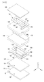
- FIG. 1 is a perspective view showing an antenna apparatus according to the embodiment.
- FIG. 2 is an exploded perspective view showing the antenna apparatus according to the embodiment.
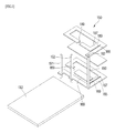
- FIG. 3 is a perspective view showing an antenna element of the antenna apparatus according to the embodiment.
- FIG. 4 is a circuit diagram showing an equivalent circuit of the antenna element according to the embodiment.
- the antenna apparatus 100 of the embodiment includes a drive substrate 110, a ground plate 130, a mounting member 140, and an antenna element 150.
- the drive substrate 110 serves as a power feeder and a supporter in the antenna apparatus 100.
- the drive substrate 110 may include a printed circuit board (PCB).
- the drive substrate 110 has a flat plate structure.
- the drive substrate 110 may be prepared as a single substrate, or maybe prepared by laminating a plurality of substrates.
- a transmission line (not shown) is embedded in the drive substrate 110. The transmission line is connected to an external power supply (not shown) of the antenna apparatus 100 through one end thereof.
- the drive substrate 110 includes a dielectric substance.
- the drive substrate 110 may include a dielectric substance having conductivity ( ⁇ ) of 0.02 and permittivity ( ⁇ ) of 4.6.
- the drive substrate 110 includes a bottom surface 111, a top surface 113 corresponding to the lower substrate 111, and a lateral side 115 connecting the top surface 113 to the bottom surface 111.
- the drive substrate 110 is divided into a ground region 117 and a device region 119.
- the drive substrate 110 includes a feeding pad 120.
- the feeding pad 120 is disposed at the device region 119 on the top surface of the drive substrate 110.
- the feeding pad 120 is connected to an opposite end of the transmission line. That is, when a signal is supplied from an external power supply, power is fed to the feeding pad 120 through the transmission line.
- the ground plate 130 of the antenna apparatus 100 is provided for the purpose of grounding.
- the ground plate 130 has a flat plate structure. Further, the ground plate 130 is disposed at the ground region 117 of the drive substrate 110. In addition, the ground plate 130 is spaced apart from the feeding pad 120 and does not make contact with the feeding pad 120. In this case, the ground plate 130 may be disposed in at least one of the top surface 113 and the bottom surface 111 of the drive substrate 110. The ground plate 130 may cover the ground region 117. When the drive substrate 110 includes a plurality of substrates, the ground plate 130 may be disposed between the substrates.
- the mounting member 140 is provided for mounting the antenna element 150 in the antenna apparatus 100.
- the mounting member 140 has a flat plate structure.
- the mounting member 140 is disposed at the device region 119 on the top surface of the drive substrate 110. In this case, the mounting member 140 covers the feeding pad 120. Further, the mounting member 140 may protrude from the device region 119 to the ground region 177 on the top surface 133 of the drive substrate 110. In this case, the mounting member 140 may overlap with the ground plate 130.
- the mounting member 140 includes a dielectric substance.
- the mounting member 140 may include a dielectric substance having the property the same as that of the drive substrate 110, or may include a dielectric substance having a property different from that of the drive substrate 110. Further, the mounting member 140 may include a dielectric substance of a high loss ratio. For example, the mounting member 140 may include a dielectric substance having conductivity of 0.02 and permittivity of 4.6.
- the mounting member 140 includes a bottom plate 141, a lower plate 143, an intermediate plate 145, an upper plate 147, and an outer plate 149.
- the bottom plate 141, the lower plate 143, the intermediate plate 145, the upper plate 147, and the outer plate 149 have a flat plate structure.
- the bottom plate 141, the lower plate 143, the intermediate plate 145, the upper plate 147, and the outer plate 149 are sequentially laminated. That is, the lower plate 143 is laminated on the bottom plate 141, the intermediate plate 145 is laminated on the lower plate 143, the upper plate 147 is laminated on the intermediate plate 145, and the outer plate 149 is laminated on the upper plate 147.
- the bottom plate 141 may adhere to the drive substrate 110.
- the bottom plate 141, the lower plate 143, the intermediate plate 145, the upper plate 147, and the outer plate 149 are laminated in one axis direction, for example, a z axis direction.
- the bottom plate 141, the lower plate 143, the intermediate plate 145, the upper plate 147, and the outer plate 149 may have the same area on a plane, for example, an x-y plane vertical to one axis.
- the antenna element 150 is provided to transmit/receive a signal in the antenna apparatus 100.
- the antenna element 150 operates at a preset resonance frequency band to transmit/receive an electromagnetic wave.
- the resonance frequency band of the antenna element 150 may be divided into a low frequency band and a high frequency band.
- the resonance frequency band may be a multi-frequency band where a low frequency band is separated from a high frequency band based on the frequency.
- the resonance frequency band may be a wide frequency band where the low frequency band is coupled with the high frequency band based on the frequency.
- the antenna element 150 resonates at preset impedance.
- the antenna element 150 is disposed at the device region 119 on the top surface 113 of the drive substrate 110. In this case, the antenna element 150 is connected to the feeding pad 120.
- the antenna element 150 has a structure branched from the feeding pad 120.
- the antenna element 150 may include a metamaterial structure.
- the metamaterial signifies an artificially synthesized material or electromagnetic structure that represents specific electromagnetic properties rarely found in nature.
- the metamaterial has negative conductivity and negative permittivity under the specific condition, and represents an electromagnetic transmission characteristic different from that of a general material or the electromagnetic structure. That is, in the embodiment, a metamaterial structure is adopted to use a characteristic where phase speed of an electromagnetic wave is inverted and the metamaterial structure has a Composite Right/Left Handed (CRLH) structure.
- CTLH Composite Right/Left Handed
- the CRLH structure includes a combination of a Right Handed (RH) structure, in which an electric field, a magnetic field, and a propagation direction of an electromagnetic wave represent general characteristics according to the right-handed law, and a Left Handed (LH) structure, in which an electric field, a magnetic field, and a propagation direction of an electromagnetic wave represent characteristics according to the left-handed law opposite to the right-handed law.
- RH Right Handed
- LH Left Handed
- the antenna element 150 may adhere to the mounting member 140.
- the antenna element 150 is inserted into the mounting member 140.
- the antenna element 150 includes a lower antenna element 160, an intermediate ground element 170, an upper antenna element 180, a feeding element 190, a ground via 191, and a feeding via 192.
- the lower antenna element 160 transmits/receives a low frequency signal in the resonance frequency band.
- the lower antenna element 160 operates at the low frequency band to transmit/receive an electromagnetic wave.
- the lower antenna element 160 is displayed at the lower plate 143. That is, the lower antenna element 160 is disposed between the lower plate 143 and the intermediate plate 145.
- the lower antenna element 160 may be formed in a patch type and then be attached to the lower plate 143.
- the lower antenna element 160 may be drawn with a conductive ink so as to be disposed at the lower plate 143.
- the lower antenna element 160 may be patterned on the lower plate 143.
- the lower antenna element 160 may include at least one of a bar type antenna element, a meander type antenna element, a spiral type antenna element, a step type antenna element, and a loop type antenna element.
- the lower antenna element 160 may include a conductive material.
- the lower antenna element 160 may include at least one of silver (Ag), palladium (Pd), platinum (Pt), copper (Cu), gold (Au), and nickel (Ni).
- the lower antenna element 160 includes a ground point 161, a lower feeding point 162, and a connection point 163.
- the ground point 161 is provided to ground the lower antenna element 160.
- the ground point 161 is connected to the ground plate 130.
- the lower feeding point 162 is provided to feed power to the lower antenna element 160.
- the lower feeding point 162 is connected to the feeding pad 120.
- the connecting point 163 is provided for external connection of the antenna element 160.
- the connecting point 163 is connected to one end of the feeding element 190.
- the ground point 161 may be disposed at one end of the lower antenna element 160.
- the lower antenna element 160 may extend while sequentially connecting the ground point 161, the lower feeding point 162, and the connecting point 163 with each other. Further, the lower antenna element 160 maybe open at an opposite end thereof.
- the lower antenna element 160 includes a lower main element 165 and a lower sub-element 167.
- the lower main element 165 extends while connecting the ground point 161, the lower feeding point 162, and the connecting point 163 with each other.
- the lower main element 165 extends along one route.
- the lower main element 165 includes one end and an opposite end of the lower antenna element 160.
- the lower sub-element 167 is connected to the lower main element 165.
- the lower sub-element 167 protrudes from the lower main element 165.
- the lower sub-element 167 extends through a route different from the route of the lower main element 165.
- at least one lower slot 169 is formed between the lower main element 165 and the lower sub-element 167.
- the intermediate ground element 170 controls electromagnetic coupling between the lower antenna element 160 and the upper antenna element 180. That is, the intermediate ground element 170 suppresses mutual interference according to driving of the lower antenna element 160 and the upper antennal element 180.
- the intermediate ground element 170 is disposed at the intermediate plate 145. That is, the intermediate ground element 170 is disposed between the intermediate plate 145 and the upper plate 147. In this case, the intermediate ground element 170 is spaced apart from the lower antenna element 160 by the intermediate plate 145. In addition, the intermediate ground element 170 overlaps with the lower antenna element 160 while interposing the intermediate plate 145 therebetween as a boundary.
- the upper antenna element 180 transmits/receives a high frequency signal in the resonance frequency band.
- the upper antenna element 180 operates at the high frequency band to transmit/receive an electromagnetic wave.
- the upper antenna element 160 is displayed at the upper plate 147. That is, the upper antenna element 180 is disposed between the upper plate 147 and the outer plate 149. In this case, the upper antenna element 180 is spaced apart from the intermediate ground element 170 by the upper plate 147. Further, the upper antenna element 180 overlaps with the intermediate ground element 170 while interposing the upper plate 147 therebetween as a boundary.
- the upper antenna element 180 may be formed in a patch type and then is attached to the lower plate 143.
- the upper antenna element 180 maybe drawn with a conductive ink so as to be disposed at the upper plate 147.
- the upper antenna element 180 may be patterned on the upper plate 147.
- the lower antenna element 160 may include at least one of a bar type antenna element, a meander type antenna element, a spiral type antenna element, a step type antenna element, and a loop type antenna element.
- the upper antenna element 160 may include a conductive material.
- the upper antenna element 180 may include at least one of silver (Ag), palladium (Pd), platinum (Pt), copper (Cu), gold (Au), and nickel (Ni).
- the upper antenna element 180 includes an upper feeding point 182.
- the upper feeding point 182 is provided to feed power to the upper antenna element 180.
- the upper feeding point 182 is connected to an opposite end of the feeding element 190.
- the upper feeding point 182 maybe disposed at one end of the upper antenna element 180.
- the upper antenna element 180 may extend from the upper feeding point 182.
- an opposite end of the upper antenna element 180 may be open.
- the upper antenna element 180 includes an upper main element 185 and an upper sub-element 187.
- the upper main element 185 includes the upper feeding point 182 and extends along one route.
- the upper main element 185 includes one end and an opposite end of the upper antenna element 180.
- the upper sub-element 187 is connected to the upper main element 185. In this case, the upper sub-element 187 protrudes from the upper main element 185. Further, the upper sub-element 187 extends through a route different from the route of the upper main element 185.
- at least one upper slot 189 is formed between the upper main element 185 and the upper sub-element 187.
- the feeding element 190 transfers a signal from the lower antenna element 160 to the upper antenna element 180.
- the feeding element 190 passes through the intermediate plate 145 and the upper plate 147. Further, the feeding element 190 is connected to the lower antenna element 160 and the upper antenna element 180.
- the feeding element 190 connects the upper feeding point 182 of the upper antenna element 180 to the connecting point 163 of the lower antenna element 160. That is, one end of the feeding element 190 makes contact with the connecting point 163, and an opposite end of the feeding element 190 makes contact with the upper feeding point 182.
- the feeding element 190 is separated from the intermediate ground element 170 so that the feeding element 190 does not make contact with the intermediate ground element 170.
- the feeding element 190 may further extend by passing through at least one of the bottom plate 141, the lower plate 143, and the outer plate 149. In this case, the feeding element 190 does not make contact with the ground plate 130.
- the feeding element 190 may be formed by inserting a conductive material into a through hole.
- the feeding element 190 may include at least one of silver (Ag), palladium (Pd), platinum (Pt), copper (Cu), gold (Au), and nickel (Ni).
- the ground via 191 is used to ground the lower antenna element 160.
- the ground via 191 is formed through the bottom plate 141 and the lower plate 143. Further, the ground via 191 connects the lower antenna element 160 to the ground plate 130.
- the ground via 191 connects the ground point 161 of the lower antenna element 160 to the ground plate 130. That is, one end of the ground via 191 makes contact with the ground plate 130, and an opposite end of the ground via 191 makes contact with the ground point 161.
- the ground via 191 may further extend through at least one of the intermediate plate 145, the upper plate 147, and the outer plate 149.
- the ground via 191 may be formed by inserting a conductive material into a through hole.
- the ground via 191 may include at least one of silver (Ag), palladium (Pd), platinum (Pt), copper (Cu), gold (Au), and nickel (Ni).
- the feeding via 192 supplies a signal to the lower antenna element 160.
- the feeding via 192 is formed through the bottom plate 141 and the lower plate 143. Further, the feeding via 192 connects the lower antenna element 160 to the feeding pad 120 of the drive substrate 110.
- the feeding via 192 connects the lower feeding point 162 of the lower antenna element 160 to the feeding pad 120. That is, one end of the feeding via 192 makes contact with the feeding pad 120, and an opposite end of the feeding via 192 makes contact with the lower feeding point 162. In this case, the feeding via 192 does not make contact with the ground plate 130.
- the feeding via 192 may further extend through at least one of the intermediate plate 145, the upper plate 147, and the outer plate 149. In this case, the feeding via 192 is separated from the intermediate ground element 170 so that the feeding via 192 does not make contact with the intermediate feeding element 170.
- the feeding via 192 may be formed by inserting a conductive material into a through hole.
- the ground via 192 may include at least one of silver (Ag), palladium (Pd), platinum (Pt), copper (Cu), gold (Au), and nickel (Ni).
- a signal is supplied from the feeding pad 120 to the antenna element 150.
- the signal of the feeding pad 120 branches from the antenna element 150 to the lower antenna element 160 and the upper antenna element 180.
- the feeding via 192 transfers the signal to the lower antenna element 160.
- the feeding via 192 transfers the signal to the lower feeding point 162.
- the signal is transferred to the lower main element 165 from the lower feeding point 162.
- the signal is introduced into the lower sub-element 167 from the lower main element 165. Accordingly, the lower antenna element 160 is driven according to the signal. That is, the lower antenna element 160 operates at a low frequency band to transmit/receive an electromagnetic wave.
- the lower antenna element 160 transfers the signal to the upper antenna element 180.
- the signal is introduced into the feeding element 190 from the lower main element 165. That is, the signal is transferred to the feeding element 190 from the connecting point 163.
- the feeding element 190 transfers the signal to the upper antennal element 180.
- the signal is transferred from the upper feeding point 182 to the upper main element 185.
- the signal is introduced from the upper main element 185 into the upper sub-element 187. Accordingly, the lower antenna element 180 is driven according to the signal. That is, the lower antenna element 180 operates at a high frequency band to transmit/receive the electromagnetic wave.
- the antenna apparatus 100 is designed to have predetermined inductance and capacitance to be operated at a resonance frequency band.
- the antenna apparatus 100 may be expressed by an equivalent circuit as shown in FIG. 4 . That is, the antenna apparatus 100 includes a serial inductor L R , a serial capacitor C L , a parallel capacitor C R , and a parallel inductor L L .
- the serial inductor L R is connected with the serial capacitor C L in series.
- the parallel capacitor C R and the parallel inductor L L are connected with the serial inductor L R and the serial capacitor C L in parallel.
- the serial inductor L R and the parallel capacitor C R represent a characteristic of the RH structure
- the serial capacitor C L and the parallel inductor L L represent a characteristic of the LH structure.
- the characteristic of the antenna apparatus 100 corresponding to the equivalent circuit is determined according to a structure or a shape of the antenna apparatus 100.
- a characteristic such as the serial inductor L R
- an area that is, a length and a width of the lower antenna element 160.
- a characteristic such as the parallel inductor L L
- a characteristic, such as the serial capacitor C L is determined according to a size of a lower slot 169 in the lower antenna element 160 and a size of an upper slot 189 in the upper antenna element 180.
- a characteristic such as the parallel capacitor C R is determined according to a spacing distance and an overlapping area between the lower antenna element 160 and the intermediate ground element 170, and a spacing distance and an overlapping area between the upper antenna element 180 and the intermediate ground element 170.
- a characteristic, such as the parallel capacitor C R is determined according to a spacing distance between the lower antenna element 160 and the ground plate 130 and a spacing distance between the upper antenna element 180 and the ground plate 130.
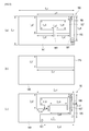
- FIG. 5 shows plan views illustrating sizes of the antenna apparatus according to the embodiment.
- FIG. 5(a) is a plan view illustrating the upper antenna element
- FIG. 5(b) is a plan view illustrating the intermediate ground element
- FIG. 5(c) is a plan view illustrating the lower antenna element.
- a mounting member 140 has a rectangular shape.
- the mounting member 140 may have a width (A_x) of 13.5 mm in an x axis direction, a width (A_y) of 6 mm in a y axis direction, and a thickness (A_h) of 2.2 mm in a z axis direction.
- the upper main element 185 extends from an upper feeding point 182 in the -y axis direction, -x axis direction, y axis direction, and x axis direction.
- the upper sub-element 187 extends in the y axis direction and the -x axis direction from the upper main element 185 extending in the -x axis direction.
- at least one upper slot 189 is formed between the upper main element 185 and the upper sub-element 187.
- the intermediate ground element 170 has a rectangular flat shape.
- the lower main element 165 extends from the ground point 161 in the x axis direction, -y axis direction, -x axis direction, y direction, and x axis direction.
- the lower sub-element 167 extends in the y axis direction and -x axis direction from the lower main element 165 extending in the -x axis direction.
- at least one lower slot 169 is formed between the lower main element 165 and the lower sub-element 167.
- FIG. 6 is a graph illustrating operation characteristics of the antenna apparatus according to the embodiment.
- FIG. 6 illustrates a frequency response characteristic of the antenna apparatus. That is, FIG. 6 illustrates variation of an S parameter according to a frequency band.
- the S parameter is a factor signifying a voltage ratio between input and output (output voltage/input voltage) at a specific frequency band, and is expressed by a dB scale.
- the antenna apparatus 100 has a resonance frequency band with an expanded bandwidth.
- the resonance frequency band represents a frequency band of -5 dB or less.
- the resonance frequency band of the antenna apparatus 100 has a bandwidth of approximately 0.54 GHz.
- the resonance frequency band of the antenna apparatus 100 is in the range of about 2.38 GHz to about 2.92 GHz.
- the antenna apparatus 100 has relatively high operation efficiency at a frequency band in the range of 2.42 GHz to 2.73 GHz among the resonance frequency band. In this case, the antenna apparatus 100 has operation efficiency of 70 % at 2.42 GHz, 58 % at 2.48 GHz, 56 % at 2.54 GHz, 84 % at 2.6 GHz, and 75% at 2.72 GHz.
- FIGS. 7 , 8 and 9 are graphs illustrating operation characteristics depending on tuning of the antenna apparatus according to the embodiment.
- FIGS. 7 , 8 and 9 illustrate a frequency response characteristic of the antenna apparatus. That is, FIGS. 7 , 8 and 9 illustrate variation of an S parameter according to a frequency band.
- a resonance frequency band may be adjusted by tuning the lower antenna element 160. That is, as shown in FIG. 7 , a frequency location of a low frequency band may be changed, and a low frequency bandwidth may be expanded or contracted.
- the low frequency may be adjusted in the lower antenna element 160 by adjusting an area of the lower antenna element 160 or a size of the lower slot 169.
- the low frequency band may be adjusted by adjusting a spacing distance and an overlapping area between the lower antenna element 160 and the intermediate ground element 170.
- the low frequency band may be adjusted by adjusting a spacing distance between the lower antenna element 160 and the ground plate 130.
- a resonance frequency band may be adjusted by tuning the upper antenna element 180. That is, as shown in FIG. 8 , a frequency location of a high frequency band may be changed, and a high frequency bandwidth may be expanded or contracted. As shown in FIG. 9 , the high frequency bandwidth may be expanded to at least two. In this case, the high frequency may be adjusted in the upper antenna element 180 by adjusting an area of the upper antenna element 180 or a size of the upper slot 189. The high frequency band may be adjusted by adjusting a spacing distance and an overlapping area between the upper antenna element 180 and the intermediate ground element 170. The high frequency band may be adjusted by adjusting a spacing distance between the upper antenna element 180 and the ground plate 130.
- the antenna apparatus includes the lower antenna element and the upper antenna element so that the antenna apparatus may have an expanded resonance frequency band. Further, since the lower antenna element is laminated on the lower antenna element in the antenna apparatus, the size of the antenna apparatus is not increased. In addition, the intermediate ground element suppresses electromagnetic coupling between the lower antenna element and the upper antenna element in the antenna apparatus, degradation in performance of the antenna apparatus can be prevented. Accordingly, a communication terminal can use an expanded resonance frequency band through a single antenna apparatus. Therefore, it is not necessary to provide a plurality of antenna apparatuses in the communication terminal so that the communication terminal can be miniaturized.
Landscapes
- Engineering & Computer Science (AREA)
- Computer Networks & Wireless Communication (AREA)
- Variable-Direction Aerials And Aerial Arrays (AREA)
- Details Of Aerials (AREA)
- Waveguide Aerials (AREA)
Abstract
Description
- The embodiment relates to an antenna apparatus, and more particularly, to an antenna apparatus of a communication terminal.
- In general, a wireless communication system provides various multimedia services such as a Global Positioning System (GPS), blue-tooth, and Internet. In this case, in order for the wireless communication system to easily provide the multimedia services, a high transmission rate of a large amount of data must be ensured. To this end, researches and studies have been carried out in order to improve the performance of an antenna apparatus in a communication terminal. This is because the antenna apparatus substantially transmits/receives data in the communication terminal. The antenna apparatus may operate at a corresponding resonance frequency band to transmit/receive the data.
- However, a resonance frequency band is narrow in the above antenna apparatus. Accordingly, the communication terminal includes a plurality of antenna apparatuses so that the resonance frequency band may be expanded. However, since the communication terminal requires a space for installing the antenna apparatuses, it is difficult to miniaturize the communication terminal. That is, the communication terminal cannot use a relatively wide resonance frequency band through a single antenna apparatus.
- The embodiment provides an antenna apparatus having a relatively wide resonance frequency band. That is, the embodiment expands a resonance frequency band of the antenna apparatus while miniaturizing the antenna apparatus.
- According to the embodiment, there is provided an antenna apparatus including: a lower antenna element; an upper antenna element on the lower antenna element; and an intermediate ground element interposed between the lower antenna element and the upper antenna element and overlapping with the lower antenna element and the upper antenna element.
- The antenna apparatus may further include a feeding element connecting the upper antenna element to the lower antenna element, and transferring a signal supplied to the lower antenna element to the upper antenna element.
- According to the embodiment, there is provided an antenna apparatus including: a lower plate; a lower antenna element on the lower plate; an intermediate plate laminated on the lower plate and the lower antenna element; an intermediate ground element disposed at the intermediate plate, and overlapping with the lower antenna element while interposing the intermediate plate therebetween as a boundary; an upper plate laminated on the intermediate plate and the intermediate ground element; and an upper antenna element disposed at the upper plate, and overlapping with the intermediate ground element while interposing the upper plate therebetween as a boundary.
- The antenna apparatus may further include a feeding element extending by passing through the intermediate plate and the upper plate to connect the upper antenna element with the lower antenna element, and transferring a signal supplied to the lower antenna element to the upper antenna element.
- The antenna apparatus according to the embodiment includes the lower antenna element and the upper antenna element so that the antenna apparatus may have an expanded resonance frequency band. Further, since the upper antenna element is laminated on the lower antenna element in the antenna apparatus, the size of the antenna apparatus is not increased. In addition, the intermediate ground element suppresses electromagnetic coupling between the lower antenna element and the upper antenna element in the antenna apparatus, so degradation in performance of the antenna apparatus can be prevented. Accordingly, a communication terminal can use an expanded resonance frequency band through a single antenna apparatus. Therefore, it is not necessary to provide a plurality of antenna apparatuses in a communication terminal so that the communication terminal can be miniaturized.
-
-
FIG. 1 is a perspective view showing an antenna apparatus according to the embodiment; -
FIG. 2 is an exploded perspective view showing the antenna apparatus according to the embodiment; -
FIG. 3 is a perspective view showing an antenna element of the antenna apparatus according to the embodiment; -
FIG. 4 is a circuit diagram showing an equivalent circuit of the antenna element according to the embodiment; -
FIG. 5 shows plan views illustrating sizes of the antenna apparatus according to the embodiment; -
FIG. 6 is a graph illustrating an operation characteristic of the antenna apparatus according to the embodiment; and -
FIGS. 7 ,8 and 9 are graphs illustrating variation in the operation characteristic depending on tuning of the antenna apparatus according to the embodiment. - Hereinafter, the embodiment will be described with reference to accompanying drawings in detail. In the following description, for the illustrative purpose, the same components will be assigned with the same reference numerals, and the repetition in the description about the same components will be omitted in order to avoid redundancy. Detailed descriptions of well-known functions and structures incorporated herein may be omitted to avoid obscuring the subject matter of the present invention.
-
FIG. 1 is a perspective view showing an antenna apparatus according to the embodiment.FIG. 2 is an exploded perspective view showing the antenna apparatus according to the embodiment.FIG. 3 is a perspective view showing an antenna element of the antenna apparatus according to the embodiment.FIG. 4 is a circuit diagram showing an equivalent circuit of the antenna element according to the embodiment. - Referring to
FIGS. 1 ,2 , and3 , theantenna apparatus 100 of the embodiment includes adrive substrate 110, aground plate 130, amounting member 140, and anantenna element 150. - The
drive substrate 110 serves as a power feeder and a supporter in theantenna apparatus 100. Thedrive substrate 110 may include a printed circuit board (PCB). Thedrive substrate 110 has a flat plate structure. In this case, thedrive substrate 110 may be prepared as a single substrate, or maybe prepared by laminating a plurality of substrates. Further, a transmission line (not shown) is embedded in thedrive substrate 110. The transmission line is connected to an external power supply (not shown) of theantenna apparatus 100 through one end thereof. - In this case, the
drive substrate 110 includes a dielectric substance. For example, thedrive substrate 110 may include a dielectric substance having conductivity (σ) of 0.02 and permittivity (ε) of 4.6. - The
drive substrate 110 includes abottom surface 111, atop surface 113 corresponding to thelower substrate 111, and alateral side 115 connecting thetop surface 113 to thebottom surface 111. Thedrive substrate 110 is divided into aground region 117 and adevice region 119. Further, thedrive substrate 110 includes afeeding pad 120. Thefeeding pad 120 is disposed at thedevice region 119 on the top surface of thedrive substrate 110. Thefeeding pad 120 is connected to an opposite end of the transmission line. That is, when a signal is supplied from an external power supply, power is fed to thefeeding pad 120 through the transmission line. - The
ground plate 130 of theantenna apparatus 100 is provided for the purpose of grounding. Theground plate 130 has a flat plate structure. Further, theground plate 130 is disposed at theground region 117 of thedrive substrate 110. In addition, theground plate 130 is spaced apart from thefeeding pad 120 and does not make contact with thefeeding pad 120. In this case, theground plate 130 may be disposed in at least one of thetop surface 113 and thebottom surface 111 of thedrive substrate 110. Theground plate 130 may cover theground region 117. When thedrive substrate 110 includes a plurality of substrates, theground plate 130 may be disposed between the substrates. - The
mounting member 140 is provided for mounting theantenna element 150 in theantenna apparatus 100. The mountingmember 140 has a flat plate structure. The mountingmember 140 is disposed at thedevice region 119 on the top surface of thedrive substrate 110. In this case, the mountingmember 140 covers thefeeding pad 120. Further, the mountingmember 140 may protrude from thedevice region 119 to the ground region 177 on the top surface 133 of thedrive substrate 110. In this case, the mountingmember 140 may overlap with theground plate 130. - In this case, the mounting
member 140 includes a dielectric substance. The mountingmember 140 may include a dielectric substance having the property the same as that of thedrive substrate 110, or may include a dielectric substance having a property different from that of thedrive substrate 110. Further, the mountingmember 140 may include a dielectric substance of a high loss ratio. For example, the mountingmember 140 may include a dielectric substance having conductivity of 0.02 and permittivity of 4.6. - In addition, the mounting
member 140 includes abottom plate 141, alower plate 143, anintermediate plate 145, anupper plate 147, and anouter plate 149. Thebottom plate 141, thelower plate 143, theintermediate plate 145, theupper plate 147, and theouter plate 149 have a flat plate structure. Further, thebottom plate 141, thelower plate 143, theintermediate plate 145, theupper plate 147, and theouter plate 149 are sequentially laminated. That is, thelower plate 143 is laminated on thebottom plate 141, theintermediate plate 145 is laminated on thelower plate 143, theupper plate 147 is laminated on theintermediate plate 145, and theouter plate 149 is laminated on theupper plate 147. Thebottom plate 141 may adhere to thedrive substrate 110. - The
bottom plate 141, thelower plate 143, theintermediate plate 145, theupper plate 147, and theouter plate 149 are laminated in one axis direction, for example, a z axis direction. Thebottom plate 141, thelower plate 143, theintermediate plate 145, theupper plate 147, and theouter plate 149 may have the same area on a plane, for example, an x-y plane vertical to one axis. - The
antenna element 150 is provided to transmit/receive a signal in theantenna apparatus 100. In this case, theantenna element 150 operates at a preset resonance frequency band to transmit/receive an electromagnetic wave. The resonance frequency band of theantenna element 150 may be divided into a low frequency band and a high frequency band. The resonance frequency band may be a multi-frequency band where a low frequency band is separated from a high frequency band based on the frequency. In addition, the resonance frequency band may be a wide frequency band where the low frequency band is coupled with the high frequency band based on the frequency. In addition, theantenna element 150 resonates at preset impedance. - The
antenna element 150 is disposed at thedevice region 119 on thetop surface 113 of thedrive substrate 110. In this case, theantenna element 150 is connected to thefeeding pad 120. Theantenna element 150 has a structure branched from thefeeding pad 120. In addition, theantenna element 150 may include a metamaterial structure. - The metamaterial signifies an artificially synthesized material or electromagnetic structure that represents specific electromagnetic properties rarely found in nature. The metamaterial has negative conductivity and negative permittivity under the specific condition, and represents an electromagnetic transmission characteristic different from that of a general material or the electromagnetic structure. That is, in the embodiment, a metamaterial structure is adopted to use a characteristic where phase speed of an electromagnetic wave is inverted and the metamaterial structure has a Composite Right/Left Handed (CRLH) structure. The CRLH structure includes a combination of a Right Handed (RH) structure, in which an electric field, a magnetic field, and a propagation direction of an electromagnetic wave represent general characteristics according to the right-handed law, and a Left Handed (LH) structure, in which an electric field, a magnetic field, and a propagation direction of an electromagnetic wave represent characteristics according to the left-handed law opposite to the right-handed law.
- Moreover, the
antenna element 150 may adhere to the mountingmember 140. Theantenna element 150 is inserted into the mountingmember 140. Further, theantenna element 150 includes alower antenna element 160, anintermediate ground element 170, anupper antenna element 180, afeeding element 190, a ground via 191, and a feeding via 192. - The
lower antenna element 160 transmits/receives a low frequency signal in the resonance frequency band. In this case, thelower antenna element 160 operates at the low frequency band to transmit/receive an electromagnetic wave. Thelower antenna element 160 is displayed at thelower plate 143. That is, thelower antenna element 160 is disposed between thelower plate 143 and theintermediate plate 145. - In this case, the
lower antenna element 160 may be formed in a patch type and then be attached to thelower plate 143. Thelower antenna element 160 may be drawn with a conductive ink so as to be disposed at thelower plate 143. Thelower antenna element 160 may be patterned on thelower plate 143. Thelower antenna element 160 may include at least one of a bar type antenna element, a meander type antenna element, a spiral type antenna element, a step type antenna element, and a loop type antenna element. In this case, thelower antenna element 160 may include a conductive material. Thelower antenna element 160 may include at least one of silver (Ag), palladium (Pd), platinum (Pt), copper (Cu), gold (Au), and nickel (Ni). - In addition, the
lower antenna element 160 includes aground point 161, alower feeding point 162, and aconnection point 163. Theground point 161 is provided to ground thelower antenna element 160. In this case, theground point 161 is connected to theground plate 130. Thelower feeding point 162 is provided to feed power to thelower antenna element 160. In this case, thelower feeding point 162 is connected to thefeeding pad 120. The connectingpoint 163 is provided for external connection of theantenna element 160. In this case, the connectingpoint 163 is connected to one end of thefeeding element 190. Theground point 161 may be disposed at one end of thelower antenna element 160. In addition, thelower antenna element 160 may extend while sequentially connecting theground point 161, thelower feeding point 162, and the connectingpoint 163 with each other. Further, thelower antenna element 160 maybe open at an opposite end thereof. - In addition, the
lower antenna element 160 includes a lowermain element 165 and alower sub-element 167. The lowermain element 165 extends while connecting theground point 161, thelower feeding point 162, and the connectingpoint 163 with each other. In this case, the lowermain element 165 extends along one route. The lowermain element 165 includes one end and an opposite end of thelower antenna element 160. Thelower sub-element 167 is connected to the lowermain element 165. In this case, thelower sub-element 167 protrudes from the lowermain element 165. Further, thelower sub-element 167 extends through a route different from the route of the lowermain element 165. In addition, at least onelower slot 169 is formed between the lowermain element 165 and thelower sub-element 167. - The
intermediate ground element 170 controls electromagnetic coupling between thelower antenna element 160 and theupper antenna element 180. That is, theintermediate ground element 170 suppresses mutual interference according to driving of thelower antenna element 160 and the upperantennal element 180. Theintermediate ground element 170 is disposed at theintermediate plate 145. That is, theintermediate ground element 170 is disposed between theintermediate plate 145 and theupper plate 147. In this case, theintermediate ground element 170 is spaced apart from thelower antenna element 160 by theintermediate plate 145. In addition, theintermediate ground element 170 overlaps with thelower antenna element 160 while interposing theintermediate plate 145 therebetween as a boundary. - The
upper antenna element 180 transmits/receives a high frequency signal in the resonance frequency band. In this case, theupper antenna element 180 operates at the high frequency band to transmit/receive an electromagnetic wave. Theupper antenna element 160 is displayed at theupper plate 147. That is, theupper antenna element 180 is disposed between theupper plate 147 and theouter plate 149. In this case, theupper antenna element 180 is spaced apart from theintermediate ground element 170 by theupper plate 147. Further, theupper antenna element 180 overlaps with theintermediate ground element 170 while interposing theupper plate 147 therebetween as a boundary. - In this case, the
upper antenna element 180 may be formed in a patch type and then is attached to thelower plate 143. Theupper antenna element 180 maybe drawn with a conductive ink so as to be disposed at theupper plate 147. Theupper antenna element 180 may be patterned on theupper plate 147. Thelower antenna element 160 may include at least one of a bar type antenna element, a meander type antenna element, a spiral type antenna element, a step type antenna element, and a loop type antenna element. In this case, theupper antenna element 160 may include a conductive material. Theupper antenna element 180 may include at least one of silver (Ag), palladium (Pd), platinum (Pt), copper (Cu), gold (Au), and nickel (Ni). - Further, the
upper antenna element 180 includes anupper feeding point 182. Theupper feeding point 182 is provided to feed power to theupper antenna element 180. In this case, theupper feeding point 182 is connected to an opposite end of thefeeding element 190. Theupper feeding point 182 maybe disposed at one end of theupper antenna element 180. Moreover, theupper antenna element 180 may extend from theupper feeding point 182. In addition, an opposite end of theupper antenna element 180 may be open. - Furthermore, the
upper antenna element 180 includes an uppermain element 185 and anupper sub-element 187. The uppermain element 185 includes theupper feeding point 182 and extends along one route. The uppermain element 185 includes one end and an opposite end of theupper antenna element 180. Theupper sub-element 187 is connected to the uppermain element 185. In this case, theupper sub-element 187 protrudes from the uppermain element 185. Further, theupper sub-element 187 extends through a route different from the route of the uppermain element 185. In addition, at least oneupper slot 189 is formed between the uppermain element 185 and theupper sub-element 187. - The
feeding element 190 transfers a signal from thelower antenna element 160 to theupper antenna element 180. Thefeeding element 190 passes through theintermediate plate 145 and theupper plate 147. Further, thefeeding element 190 is connected to thelower antenna element 160 and theupper antenna element 180. Thefeeding element 190 connects theupper feeding point 182 of theupper antenna element 180 to the connectingpoint 163 of thelower antenna element 160. That is, one end of thefeeding element 190 makes contact with the connectingpoint 163, and an opposite end of thefeeding element 190 makes contact with theupper feeding point 182. In this case, thefeeding element 190 is separated from theintermediate ground element 170 so that thefeeding element 190 does not make contact with theintermediate ground element 170. Thefeeding element 190 may further extend by passing through at least one of thebottom plate 141, thelower plate 143, and theouter plate 149. In this case, thefeeding element 190 does not make contact with theground plate 130. - In this case, the
feeding element 190 may be formed by inserting a conductive material into a through hole. Thefeeding element 190 may include at least one of silver (Ag), palladium (Pd), platinum (Pt), copper (Cu), gold (Au), and nickel (Ni). - The ground via 191 is used to ground the
lower antenna element 160. The ground via 191 is formed through thebottom plate 141 and thelower plate 143. Further, the ground via 191 connects thelower antenna element 160 to theground plate 130. The ground via 191 connects theground point 161 of thelower antenna element 160 to theground plate 130. That is, one end of the ground via 191 makes contact with theground plate 130, and an opposite end of the ground via 191 makes contact with theground point 161. The ground via 191 may further extend through at least one of theintermediate plate 145, theupper plate 147, and theouter plate 149. - In this case, the ground via 191 may be formed by inserting a conductive material into a through hole. The ground via 191 may include at least one of silver (Ag), palladium (Pd), platinum (Pt), copper (Cu), gold (Au), and nickel (Ni).
- The feeding via 192 supplies a signal to the
lower antenna element 160. The feeding via 192 is formed through thebottom plate 141 and thelower plate 143. Further, the feeding via 192 connects thelower antenna element 160 to thefeeding pad 120 of thedrive substrate 110. The feeding via 192 connects thelower feeding point 162 of thelower antenna element 160 to thefeeding pad 120. That is, one end of the feeding via 192 makes contact with thefeeding pad 120, and an opposite end of the feeding via 192 makes contact with thelower feeding point 162. In this case, the feeding via 192 does not make contact with theground plate 130. The feeding via 192 may further extend through at least one of theintermediate plate 145, theupper plate 147, and theouter plate 149. In this case, the feeding via 192 is separated from theintermediate ground element 170 so that the feeding via 192 does not make contact with theintermediate feeding element 170. - In this case, the feeding via 192 may be formed by inserting a conductive material into a through hole. The ground via 192 may include at least one of silver (Ag), palladium (Pd), platinum (Pt), copper (Cu), gold (Au), and nickel (Ni).
- In the
antenna apparatus 100, a signal is supplied from thefeeding pad 120 to theantenna element 150. The signal of thefeeding pad 120 branches from theantenna element 150 to thelower antenna element 160 and theupper antenna element 180. - That is, the feeding via 192 transfers the signal to the
lower antenna element 160. In this case, the feeding via 192 transfers the signal to thelower feeding point 162. Next, the signal is transferred to the lowermain element 165 from thelower feeding point 162. Then, the signal is introduced into the lower sub-element 167 from the lowermain element 165. Accordingly, thelower antenna element 160 is driven according to the signal. That is, thelower antenna element 160 operates at a low frequency band to transmit/receive an electromagnetic wave. - In addition, the
lower antenna element 160 transfers the signal to theupper antenna element 180. In this case, the signal is introduced into thefeeding element 190 from the lowermain element 165. That is, the signal is transferred to thefeeding element 190 from the connectingpoint 163. Further, thefeeding element 190 transfers the signal to the upperantennal element 180. The signal is transferred from theupper feeding point 182 to the uppermain element 185. In addition, the signal is introduced from the uppermain element 185 into theupper sub-element 187. Accordingly, thelower antenna element 180 is driven according to the signal. That is, thelower antenna element 180 operates at a high frequency band to transmit/receive the electromagnetic wave. - In addition, the
antenna apparatus 100 is designed to have predetermined inductance and capacitance to be operated at a resonance frequency band. In this case, theantenna apparatus 100 may be expressed by an equivalent circuit as shown inFIG. 4 . That is, theantenna apparatus 100 includes a serial inductor LR, a serial capacitor CL, a parallel capacitor CR, and a parallel inductor LL. The serial inductor LR is connected with the serial capacitor CL in series. The parallel capacitor CR and the parallel inductor LL are connected with the serial inductor LR and the serial capacitor CL in parallel. The serial inductor LR and the parallel capacitor CR represent a characteristic of the RH structure, and the serial capacitor CL and the parallel inductor LL represent a characteristic of the LH structure. - In this case, the characteristic of the
antenna apparatus 100 corresponding to the equivalent circuit is determined according to a structure or a shape of theantenna apparatus 100. For example, a characteristic, such as the serial inductor LR, is determined according to an area, that is, a length and a width of thelower antenna element 160. Further, a characteristic, such as the parallel inductor LL, is determined according to an area, a length and a width of theupper antenna element 180. A characteristic, such as the serial capacitor CL, is determined according to a size of alower slot 169 in thelower antenna element 160 and a size of anupper slot 189 in theupper antenna element 180. In addition, a characteristic such as the parallel capacitor CR is determined according to a spacing distance and an overlapping area between thelower antenna element 160 and theintermediate ground element 170, and a spacing distance and an overlapping area between theupper antenna element 180 and theintermediate ground element 170. Moreover, a characteristic, such as the parallel capacitor CR, is determined according to a spacing distance between thelower antenna element 160 and theground plate 130 and a spacing distance between theupper antenna element 180 and theground plate 130. -
FIG. 5 shows plan views illustrating sizes of the antenna apparatus according to the embodiment. In this case,FIG. 5(a) is a plan view illustrating the upper antenna element,FIG. 5(b) is a plan view illustrating the intermediate ground element, andFIG. 5(c) is a plan view illustrating the lower antenna element. - Referring to
FIG. 5 , in theantenna apparatus 100 of the embodiment, a mountingmember 140 has a rectangular shape. The mountingmember 140 may have a width (A_x) of 13.5 mm in an x axis direction, a width (A_y) of 6 mm in a y axis direction, and a thickness (A_h) of 2.2 mm in a z axis direction. - Further, in the
upper antenna element 180, the uppermain element 185 extends from anupper feeding point 182 in the -y axis direction, -x axis direction, y axis direction, and x axis direction. In addition, theupper sub-element 187 extends in the y axis direction and the -x axis direction from the uppermain element 185 extending in the -x axis direction. In this case, at least oneupper slot 189 is formed between the uppermain element 185 and theupper sub-element 187. Entire parameters in theupper antenna element 180 maybe as follows: 1_x1 = 8.5 mm, 1_x2 = 3.8 mm, 1_x3 = 3 mm, 1_y1 = 5.15 mm, 1_y2 = 3.6 mm, 1_y3 = 2 mm, 1_y4 = 2 mm, 1_g1 = 0.7 mm, 1_g2 = 0.2 mm, and 1_w = 0.8 mm. - Further, the
intermediate ground element 170 has a rectangular flat shape. The entire parameters in theintermediate ground element 170 may be as follows: 2_x1 = 8.5 mm, and 2_y1 = 2.5 mm. - In addition, in the
lower antenna element 160, the lowermain element 165 extends from theground point 161 in the x axis direction, -y axis direction, -x axis direction, y direction, and x axis direction. Further, thelower sub-element 167 extends in the y axis direction and -x axis direction from the lowermain element 165 extending in the -x axis direction. In this case, at least onelower slot 169 is formed between the lowermain element 165 and thelower sub-element 167. Entire parameters in thelower antenna element 160 maybe as follows: 3_x1 = 8.5 mm, 3_x2 = 1.8 mm, 3_x3 = 3.9 mm, 2_x4 = 4.5 mm, 3_x5 = 6.9 mm, 3_y1 = 5.15 mm, 3_y2 = 3.9 mm, 3_y3 = 2.3 mm, 3_y4 = 2.9 mm, 3_g1 = 0.2 mm, and 3_sw = 1.4 mm. -
FIG. 6 is a graph illustrating operation characteristics of the antenna apparatus according to the embodiment. In this case,FIG. 6 illustrates a frequency response characteristic of the antenna apparatus. That is,FIG. 6 illustrates variation of an S parameter according to a frequency band. The S parameter is a factor signifying a voltage ratio between input and output (output voltage/input voltage) at a specific frequency band, and is expressed by a dB scale. - Referring to
FIG. 6 , theantenna apparatus 100 has a resonance frequency band with an expanded bandwidth. The resonance frequency band represents a frequency band of -5 dB or less. In this case, the resonance frequency band of theantenna apparatus 100 has a bandwidth of approximately 0.54 GHz. The resonance frequency band of theantenna apparatus 100 is in the range of about 2.38 GHz to about 2.92 GHz. Further, theantenna apparatus 100 has relatively high operation efficiency at a frequency band in the range of 2.42 GHz to 2.73 GHz among the resonance frequency band. In this case, theantenna apparatus 100 has operation efficiency of 70 % at 2.42 GHz, 58 % at 2.48 GHz, 56 % at 2.54 GHz, 84 % at 2.6 GHz, and 75% at 2.72 GHz. -
FIGS. 7 ,8 and 9 are graphs illustrating operation characteristics depending on tuning of the antenna apparatus according to the embodiment. In this case,FIGS. 7 ,8 and 9 illustrate a frequency response characteristic of the antenna apparatus. That is,FIGS. 7 ,8 and 9 illustrate variation of an S parameter according to a frequency band. - That is, in the
antenna apparatus 100 of the embodiment, a resonance frequency band may be adjusted by tuning thelower antenna element 160. That is, as shown inFIG. 7 , a frequency location of a low frequency band may be changed, and a low frequency bandwidth may be expanded or contracted. In this case, the low frequency may be adjusted in thelower antenna element 160 by adjusting an area of thelower antenna element 160 or a size of thelower slot 169. The low frequency band may be adjusted by adjusting a spacing distance and an overlapping area between thelower antenna element 160 and theintermediate ground element 170. The low frequency band may be adjusted by adjusting a spacing distance between thelower antenna element 160 and theground plate 130. - In the
antenna apparatus 100 of the embodiment, a resonance frequency band may be adjusted by tuning theupper antenna element 180. That is, as shown inFIG. 8 , a frequency location of a high frequency band may be changed, and a high frequency bandwidth may be expanded or contracted. As shown inFIG. 9 , the high frequency bandwidth may be expanded to at least two. In this case, the high frequency may be adjusted in theupper antenna element 180 by adjusting an area of theupper antenna element 180 or a size of theupper slot 189. The high frequency band may be adjusted by adjusting a spacing distance and an overlapping area between theupper antenna element 180 and theintermediate ground element 170. The high frequency band may be adjusted by adjusting a spacing distance between theupper antenna element 180 and theground plate 130. - According to the embodiment, the antenna apparatus includes the lower antenna element and the upper antenna element so that the antenna apparatus may have an expanded resonance frequency band. Further, since the lower antenna element is laminated on the lower antenna element in the antenna apparatus, the size of the antenna apparatus is not increased. In addition, the intermediate ground element suppresses electromagnetic coupling between the lower antenna element and the upper antenna element in the antenna apparatus, degradation in performance of the antenna apparatus can be prevented. Accordingly, a communication terminal can use an expanded resonance frequency band through a single antenna apparatus. Therefore, it is not necessary to provide a plurality of antenna apparatuses in the communication terminal so that the communication terminal can be miniaturized.
- Although exemplary embodiments of the present invention have been described in detail hereinabove, it should be clearly understood that many variations and modifications of the basic inventive concepts herein taught which may appear to those skilled in the present art will still fall within the spirit and scope of the present invention, as defined in the appended claims.
Claims (15)
- An antenna apparatus comprising:a lower antenna element;an upper antenna element on the lower antenna element; andan intermediate ground element interposed between the lower antenna element and the upper antenna element and overlapping with the lower antenna element and the upper antenna element.
- The antenna apparatus of claim 1, further comprising a feeding element connecting the upper antenna element to the lower antenna element, and transferring a signal supplied to the lower antenna element to the upper antenna element.
- The antenna apparatus of claim 2, further comprising:an intermediate plate interposed between the lower antenna element and the intermediate ground element, and spacing the intermediate ground element apart from the lower antenna element; andan upper plate interposed between the intermediate ground element and the upper antenna element, and spacing the intermediate ground element apart from the upper antenna element.
- The antenna apparatus of claim 3, wherein the feeding element extends bypassing through the intermediate plate and the upper plate.
- The antenna apparatus of claim 1, wherein the lower antenna element comprises:a lower main element to which a signal is supplied; anda lower sub-element connected to the lower main element,wherein a lower slot is formed between the lower main element and the lower sub-element.
- The antenna apparatus of claim 1, wherein the upper antenna element comprises:an upper main element to which the signal is supplied from the lower antenna element; andan upper sub-element connected to the upper main element,wherein an upper slot is formed between the upper main element and the upper sub-element.
- The antenna apparatus of claim 3, further comprising a lower plate at which the lower antenna element is disposed and on which the intermediate plate and the upper plate are laminated.
- The antenna apparatus of claim 7, wherein the lower plate comprises:a feeding via formed through the lower plate to supply the signal to the lower antenna element; anda ground via formed through the lower plate to ground the lower antenna element.
- The antenna apparatus of claim 8, further comprising a bottom plate on which the lower plate is laminated, wherein the feeding via and the ground via are formed through the bottom plate.
- The antenna apparatus of claim 3, further comprising an outer plate laminated on the upper antenna element.
- The antenna apparatus of claim 1, further comprising a ground plate making contact with the lower antenna element.
- The antenna apparatus of claim 11, wherein the lower antenna element comprises a ground point making contact with the ground plate.
- An antenna apparatus comprising:a lower plate;a lower antenna element on the lower plate;an intermediate plate laminated on the lower plate and the lower antenna element;an intermediate ground element disposed at the intermediate plate, and overlapping with the lower antenna element while interposing the intermediate plate therebetween as a boundary;an upper plate laminated on the intermediate plate and the intermediate ground element; andan upper antenna element disposed at the upper plate, and overlapping with the intermediate ground element while interposing the upper plate therebetween as a boundary.
- The antenna apparatus of claim 13, further comprising a feeding element extending by passing through the intermediate plate and the upper plate to connect the upper antenna element with the lower antenna element, and transferring a signal supplied to the lower antenna element to the upper antenna element.
- The antenna apparatus of claim 14, further comprising:a bottom plate on which the lower plate is laminated;a feeding via formed through the lower plate and the bottom plate to supply the signal to the lower antenna element; anda ground via formed through the lower plate and the bottom plate to ground the lower antennal element.
Applications Claiming Priority (2)
| Application Number | Priority Date | Filing Date | Title |
|---|---|---|---|
| KR1020120079875A KR101926549B1 (en) | 2012-07-23 | 2012-07-23 | Antenna apparatus |
| PCT/KR2013/006601 WO2014017813A1 (en) | 2012-07-23 | 2013-07-23 | Antenna apparatus |
Publications (3)
| Publication Number | Publication Date |
|---|---|
| EP2876726A1 true EP2876726A1 (en) | 2015-05-27 |
| EP2876726A4 EP2876726A4 (en) | 2015-07-22 |
| EP2876726B1 EP2876726B1 (en) | 2016-09-14 |
Family
ID=49997561
Family Applications (1)
| Application Number | Title | Priority Date | Filing Date |
|---|---|---|---|
| EP13822556.0A Active EP2876726B1 (en) | 2012-07-23 | 2013-07-23 | Antenna apparatus |
Country Status (5)
| Country | Link |
|---|---|
| US (1) | US9819078B2 (en) |
| EP (1) | EP2876726B1 (en) |
| KR (1) | KR101926549B1 (en) |
| CN (1) | CN104662735B (en) |
| WO (1) | WO2014017813A1 (en) |
Cited By (1)
| Publication number | Priority date | Publication date | Assignee | Title |
|---|---|---|---|---|
| FR3096515A1 (en) * | 2019-05-23 | 2020-11-27 | Psa Automobiles Sa | Vehicle antenna system |
Families Citing this family (3)
| Publication number | Priority date | Publication date | Assignee | Title |
|---|---|---|---|---|
| TWI566465B (en) * | 2015-04-30 | 2017-01-11 | 智易科技股份有限公司 | Assembly-type dual-band printed antenna |
| KR102018176B1 (en) * | 2018-10-18 | 2019-09-04 | 서울과학기술대학교 산학협력단 | Implantable antenna for collecting bio signal |
| EP4002588B1 (en) * | 2020-11-18 | 2025-10-08 | TMY Technology Inc. | Broadband linear polarization antenna structure |
Family Cites Families (18)
| Publication number | Priority date | Publication date | Assignee | Title |
|---|---|---|---|---|
| US4131893A (en) * | 1977-04-01 | 1978-12-26 | Ball Corporation | Microstrip radiator with folded resonant cavity |
| US4827271A (en) | 1986-11-24 | 1989-05-02 | Mcdonnell Douglas Corporation | Dual frequency microstrip patch antenna with improved feed and increased bandwidth |
| JP3656470B2 (en) | 1999-08-12 | 2005-06-08 | 株式会社村田製作所 | Frequency switching structure of surface mount antenna and communication device having the structure |
| US6545572B1 (en) * | 2000-09-07 | 2003-04-08 | Hitachi Chemical Co., Ltd. | Multi-layer line interfacial connector using shielded patch elements |
| JP2002330023A (en) | 2001-04-27 | 2002-11-15 | Matsushita Electric Ind Co Ltd | Antenna device and wireless device using the same |
| FR2825837B1 (en) | 2001-06-12 | 2006-09-08 | Cit Alcatel | MULTIBAND COMPACT ANTENNA |
| KR100597581B1 (en) | 2004-11-05 | 2006-07-06 | 한국전자통신연구원 | Symmetrical Multiband Internal Antenna with Stubs |
| US7696931B2 (en) * | 2005-11-24 | 2010-04-13 | Lg Electronics, Inc. | Antenna for enhancing bandwidth and electronic device having the same |
| KR100847144B1 (en) | 2006-09-29 | 2008-07-18 | 한국전자통신연구원 | Dual band patch antenna of PCC print type and wireless communication module |
| EP1933418A1 (en) | 2006-12-15 | 2008-06-18 | Seiko Epson Corporation | Antenna tuning method based on an variable shorting means and planar antenna with variable shorting means |
| KR101038654B1 (en) * | 2009-02-26 | 2011-06-02 | 주식회사 모비텍 | Multi-array Pattern Antenna |
| KR101572037B1 (en) * | 2009-11-05 | 2015-11-26 | 엘지전자 주식회사 | Mobile terminal |
| EP2320520B1 (en) * | 2009-11-05 | 2015-12-16 | Lg Electronics Inc. | Portable terminal |
| CN101719584B (en) | 2009-12-24 | 2013-08-28 | 华为终端有限公司 | Reconfigurable mobile phone built-in antenna and implementation method thereof |
| FR2958458B1 (en) | 2010-04-02 | 2012-09-28 | Senseor | REVERSIBLE PIFA ANTENNA |
| TWI429136B (en) | 2010-04-06 | 2014-03-01 | Univ Nat Taiwan | Stacked antenna structure |
| KR101119354B1 (en) | 2010-04-13 | 2012-03-07 | 고려대학교 산학협력단 | Dielectric resonant antenna embedded in multilayer substrate for enhancing bandwidth |
| US8786496B2 (en) | 2010-07-28 | 2014-07-22 | Toyota Motor Engineering & Manufacturing North America, Inc. | Three-dimensional array antenna on a substrate with enhanced backlobe suppression for mm-wave automotive applications |
-
2012
- 2012-07-23 KR KR1020120079875A patent/KR101926549B1/en active Active
-
2013
- 2013-07-23 CN CN201380049496.5A patent/CN104662735B/en active Active
- 2013-07-23 WO PCT/KR2013/006601 patent/WO2014017813A1/en not_active Ceased
- 2013-07-23 US US14/416,974 patent/US9819078B2/en active Active
- 2013-07-23 EP EP13822556.0A patent/EP2876726B1/en active Active
Cited By (1)
| Publication number | Priority date | Publication date | Assignee | Title |
|---|---|---|---|---|
| FR3096515A1 (en) * | 2019-05-23 | 2020-11-27 | Psa Automobiles Sa | Vehicle antenna system |
Also Published As
| Publication number | Publication date |
|---|---|
| CN104662735B (en) | 2017-04-12 |
| KR101926549B1 (en) | 2019-03-12 |
| EP2876726A4 (en) | 2015-07-22 |
| CN104662735A (en) | 2015-05-27 |
| KR20140013278A (en) | 2014-02-05 |
| US9819078B2 (en) | 2017-11-14 |
| WO2014017813A1 (en) | 2014-01-30 |
| US20150207222A1 (en) | 2015-07-23 |
| EP2876726B1 (en) | 2016-09-14 |
Similar Documents
| Publication | Publication Date | Title |
|---|---|---|
| JP5934147B2 (en) | Antenna device | |
| EP2381529B1 (en) | Communications structures including antennas with separate antenna branches coupled to feed and ground conductors | |
| EP2019448A1 (en) | Antenna device | |
| EP2876726B1 (en) | Antenna apparatus | |
| KR101470117B1 (en) | Antenna apparatus | |
| EP2760077B1 (en) | Antenna apparatus and feeding structure thereof | |
| US10230149B2 (en) | Electricity feeding structure | |
| KR101480592B1 (en) | Antenna apparatus and feeding structure thereof | |
| KR20150091876A (en) | Antenna apparatus | |
| KR20140143969A (en) | Antenna apparatus and feeding structure thereof | |
| WO2007077461A1 (en) | Laptop computer antenna device | |
| KR101470086B1 (en) | Antenna apparatus | |
| KR101428204B1 (en) | Antenna apparatus and feeding structure thereof | |
| KR101417574B1 (en) | Antenna apparatus and feeding structure thereof | |
| KR101405730B1 (en) | Resonance additional device, feeding structure and antenna apparatus having the same | |
| KR101987250B1 (en) | Antenna apparatus and feeding structure thereof | |
| KR101439000B1 (en) | Antenna apparatus and feeding structure thereof | |
| KR20150007717A (en) | Antenna apparatus and feeding structure thereof |
Legal Events
| Date | Code | Title | Description |
|---|---|---|---|
| PUAI | Public reference made under article 153(3) epc to a published international application that has entered the european phase |
Free format text: ORIGINAL CODE: 0009012 |
|
| 17P | Request for examination filed |
Effective date: 20150216 |
|
| AK | Designated contracting states |
Kind code of ref document: A1 Designated state(s): AL AT BE BG CH CY CZ DE DK EE ES FI FR GB GR HR HU IE IS IT LI LT LU LV MC MK MT NL NO PL PT RO RS SE SI SK SM TR |
|
| AX | Request for extension of the european patent |
Extension state: BA ME |
|
| RA4 | Supplementary search report drawn up and despatched (corrected) |
Effective date: 20150623 |
|
| RIC1 | Information provided on ipc code assigned before grant |
Ipc: H01Q 1/38 20060101ALN20150617BHEP Ipc: H01Q 1/52 20060101ALN20150617BHEP Ipc: H01Q 5/371 20150101ALI20150617BHEP Ipc: H01Q 9/04 20060101AFI20150617BHEP Ipc: H01Q 1/24 20060101ALN20150617BHEP |
|
| DAX | Request for extension of the european patent (deleted) | ||
| REG | Reference to a national code |
Ref country code: DE Ref legal event code: R079 Ref document number: 602013011744 Country of ref document: DE Free format text: PREVIOUS MAIN CLASS: H01Q0001240000 Ipc: H01Q0009040000 |
|
| GRAP | Despatch of communication of intention to grant a patent |
Free format text: ORIGINAL CODE: EPIDOSNIGR1 |
|
| RIC1 | Information provided on ipc code assigned before grant |
Ipc: H01Q 5/371 20150101ALI20160225BHEP Ipc: H01Q 1/38 20060101ALN20160225BHEP Ipc: H01Q 1/52 20060101ALN20160225BHEP Ipc: H01Q 1/24 20060101ALN20160225BHEP Ipc: H01Q 9/04 20060101AFI20160225BHEP |
|
| INTG | Intention to grant announced |
Effective date: 20160309 |
|
| GRAS | Grant fee paid |
Free format text: ORIGINAL CODE: EPIDOSNIGR3 |
|
| GRAA | (expected) grant |
Free format text: ORIGINAL CODE: 0009210 |
|
| AK | Designated contracting states |
Kind code of ref document: B1 Designated state(s): AL AT BE BG CH CY CZ DE DK EE ES FI FR GB GR HR HU IE IS IT LI LT LU LV MC MK MT NL NO PL PT RO RS SE SI SK SM TR |
|
| REG | Reference to a national code |
Ref country code: GB Ref legal event code: FG4D |
|
| REG | Reference to a national code |
Ref country code: CH Ref legal event code: EP |
|
| REG | Reference to a national code |
Ref country code: IE Ref legal event code: FG4D |
|
| REG | Reference to a national code |
Ref country code: AT Ref legal event code: REF Ref document number: 829896 Country of ref document: AT Kind code of ref document: T Effective date: 20161015 |
|
| REG | Reference to a national code |
Ref country code: DE Ref legal event code: R096 Ref document number: 602013011744 Country of ref document: DE |
|
| REG | Reference to a national code |
Ref country code: NL Ref legal event code: FP |
|
| REG | Reference to a national code |
Ref country code: LT Ref legal event code: MG4D |
|
| PG25 | Lapsed in a contracting state [announced via postgrant information from national office to epo] |
Ref country code: RS Free format text: LAPSE BECAUSE OF FAILURE TO SUBMIT A TRANSLATION OF THE DESCRIPTION OR TO PAY THE FEE WITHIN THE PRESCRIBED TIME-LIMIT Effective date: 20160914 Ref country code: LT Free format text: LAPSE BECAUSE OF FAILURE TO SUBMIT A TRANSLATION OF THE DESCRIPTION OR TO PAY THE FEE WITHIN THE PRESCRIBED TIME-LIMIT Effective date: 20160914 Ref country code: FI Free format text: LAPSE BECAUSE OF FAILURE TO SUBMIT A TRANSLATION OF THE DESCRIPTION OR TO PAY THE FEE WITHIN THE PRESCRIBED TIME-LIMIT Effective date: 20160914 Ref country code: HR Free format text: LAPSE BECAUSE OF FAILURE TO SUBMIT A TRANSLATION OF THE DESCRIPTION OR TO PAY THE FEE WITHIN THE PRESCRIBED TIME-LIMIT Effective date: 20160914 Ref country code: NO Free format text: LAPSE BECAUSE OF FAILURE TO SUBMIT A TRANSLATION OF THE DESCRIPTION OR TO PAY THE FEE WITHIN THE PRESCRIBED TIME-LIMIT Effective date: 20161214 |
|
| REG | Reference to a national code |
Ref country code: AT Ref legal event code: MK05 Ref document number: 829896 Country of ref document: AT Kind code of ref document: T Effective date: 20160914 |
|
| PG25 | Lapsed in a contracting state [announced via postgrant information from national office to epo] |
Ref country code: SE Free format text: LAPSE BECAUSE OF FAILURE TO SUBMIT A TRANSLATION OF THE DESCRIPTION OR TO PAY THE FEE WITHIN THE PRESCRIBED TIME-LIMIT Effective date: 20160914 Ref country code: GR Free format text: LAPSE BECAUSE OF FAILURE TO SUBMIT A TRANSLATION OF THE DESCRIPTION OR TO PAY THE FEE WITHIN THE PRESCRIBED TIME-LIMIT Effective date: 20161215 Ref country code: LV Free format text: LAPSE BECAUSE OF FAILURE TO SUBMIT A TRANSLATION OF THE DESCRIPTION OR TO PAY THE FEE WITHIN THE PRESCRIBED TIME-LIMIT Effective date: 20160914 |
|
| PG25 | Lapsed in a contracting state [announced via postgrant information from national office to epo] |
Ref country code: RO Free format text: LAPSE BECAUSE OF FAILURE TO SUBMIT A TRANSLATION OF THE DESCRIPTION OR TO PAY THE FEE WITHIN THE PRESCRIBED TIME-LIMIT Effective date: 20160914 Ref country code: EE Free format text: LAPSE BECAUSE OF FAILURE TO SUBMIT A TRANSLATION OF THE DESCRIPTION OR TO PAY THE FEE WITHIN THE PRESCRIBED TIME-LIMIT Effective date: 20160914 |
|
| RAP2 | Party data changed (patent owner data changed or rights of a patent transferred) |
Owner name: LG INNOTEK CO., LTD. |
|
| PG25 | Lapsed in a contracting state [announced via postgrant information from national office to epo] |
Ref country code: IS Free format text: LAPSE BECAUSE OF FAILURE TO SUBMIT A TRANSLATION OF THE DESCRIPTION OR TO PAY THE FEE WITHIN THE PRESCRIBED TIME-LIMIT Effective date: 20170114 Ref country code: SK Free format text: LAPSE BECAUSE OF FAILURE TO SUBMIT A TRANSLATION OF THE DESCRIPTION OR TO PAY THE FEE WITHIN THE PRESCRIBED TIME-LIMIT Effective date: 20160914 Ref country code: PL Free format text: LAPSE BECAUSE OF FAILURE TO SUBMIT A TRANSLATION OF THE DESCRIPTION OR TO PAY THE FEE WITHIN THE PRESCRIBED TIME-LIMIT Effective date: 20160914 Ref country code: ES Free format text: LAPSE BECAUSE OF FAILURE TO SUBMIT A TRANSLATION OF THE DESCRIPTION OR TO PAY THE FEE WITHIN THE PRESCRIBED TIME-LIMIT Effective date: 20160914 Ref country code: BG Free format text: LAPSE BECAUSE OF FAILURE TO SUBMIT A TRANSLATION OF THE DESCRIPTION OR TO PAY THE FEE WITHIN THE PRESCRIBED TIME-LIMIT Effective date: 20161214 Ref country code: PT Free format text: LAPSE BECAUSE OF FAILURE TO SUBMIT A TRANSLATION OF THE DESCRIPTION OR TO PAY THE FEE WITHIN THE PRESCRIBED TIME-LIMIT Effective date: 20170116 Ref country code: BE Free format text: LAPSE BECAUSE OF FAILURE TO SUBMIT A TRANSLATION OF THE DESCRIPTION OR TO PAY THE FEE WITHIN THE PRESCRIBED TIME-LIMIT Effective date: 20160914 Ref country code: AT Free format text: LAPSE BECAUSE OF FAILURE TO SUBMIT A TRANSLATION OF THE DESCRIPTION OR TO PAY THE FEE WITHIN THE PRESCRIBED TIME-LIMIT Effective date: 20160914 Ref country code: CZ Free format text: LAPSE BECAUSE OF FAILURE TO SUBMIT A TRANSLATION OF THE DESCRIPTION OR TO PAY THE FEE WITHIN THE PRESCRIBED TIME-LIMIT Effective date: 20160914 Ref country code: SM Free format text: LAPSE BECAUSE OF FAILURE TO SUBMIT A TRANSLATION OF THE DESCRIPTION OR TO PAY THE FEE WITHIN THE PRESCRIBED TIME-LIMIT Effective date: 20160914 |
|
| REG | Reference to a national code |
Ref country code: DE Ref legal event code: R097 Ref document number: 602013011744 Country of ref document: DE |
|
| PG25 | Lapsed in a contracting state [announced via postgrant information from national office to epo] |
Ref country code: IT Free format text: LAPSE BECAUSE OF FAILURE TO SUBMIT A TRANSLATION OF THE DESCRIPTION OR TO PAY THE FEE WITHIN THE PRESCRIBED TIME-LIMIT Effective date: 20160914 |
|
| PLBE | No opposition filed within time limit |
Free format text: ORIGINAL CODE: 0009261 |
|
| STAA | Information on the status of an ep patent application or granted ep patent |
Free format text: STATUS: NO OPPOSITION FILED WITHIN TIME LIMIT |
|
| PG25 | Lapsed in a contracting state [announced via postgrant information from national office to epo] |
Ref country code: DK Free format text: LAPSE BECAUSE OF FAILURE TO SUBMIT A TRANSLATION OF THE DESCRIPTION OR TO PAY THE FEE WITHIN THE PRESCRIBED TIME-LIMIT Effective date: 20160914 |
|
| 26N | No opposition filed |
Effective date: 20170615 |
|
| PG25 | Lapsed in a contracting state [announced via postgrant information from national office to epo] |
Ref country code: SI Free format text: LAPSE BECAUSE OF FAILURE TO SUBMIT A TRANSLATION OF THE DESCRIPTION OR TO PAY THE FEE WITHIN THE PRESCRIBED TIME-LIMIT Effective date: 20160914 |
|
| REG | Reference to a national code |
Ref country code: CH Ref legal event code: PL |
|
| GBPC | Gb: european patent ceased through non-payment of renewal fee |
Effective date: 20170723 |
|
| REG | Reference to a national code |
Ref country code: IE Ref legal event code: MM4A |
|
| REG | Reference to a national code |
Ref country code: FR Ref legal event code: ST Effective date: 20180330 |
|
| PG25 | Lapsed in a contracting state [announced via postgrant information from national office to epo] |
Ref country code: LI Free format text: LAPSE BECAUSE OF NON-PAYMENT OF DUE FEES Effective date: 20170731 Ref country code: GB Free format text: LAPSE BECAUSE OF NON-PAYMENT OF DUE FEES Effective date: 20170723 Ref country code: CH Free format text: LAPSE BECAUSE OF NON-PAYMENT OF DUE FEES Effective date: 20170731 Ref country code: IE Free format text: LAPSE BECAUSE OF NON-PAYMENT OF DUE FEES Effective date: 20170723 |
|
| PG25 | Lapsed in a contracting state [announced via postgrant information from national office to epo] |
Ref country code: FR Free format text: LAPSE BECAUSE OF NON-PAYMENT OF DUE FEES Effective date: 20170731 |
|
| PG25 | Lapsed in a contracting state [announced via postgrant information from national office to epo] |
Ref country code: LU Free format text: LAPSE BECAUSE OF NON-PAYMENT OF DUE FEES Effective date: 20170723 |
|
| PG25 | Lapsed in a contracting state [announced via postgrant information from national office to epo] |
Ref country code: MT Free format text: LAPSE BECAUSE OF NON-PAYMENT OF DUE FEES Effective date: 20170723 |
|
| PG25 | Lapsed in a contracting state [announced via postgrant information from national office to epo] |
Ref country code: AL Free format text: LAPSE BECAUSE OF FAILURE TO SUBMIT A TRANSLATION OF THE DESCRIPTION OR TO PAY THE FEE WITHIN THE PRESCRIBED TIME-LIMIT Effective date: 20160914 |
|
| PG25 | Lapsed in a contracting state [announced via postgrant information from national office to epo] |
Ref country code: HU Free format text: LAPSE BECAUSE OF FAILURE TO SUBMIT A TRANSLATION OF THE DESCRIPTION OR TO PAY THE FEE WITHIN THE PRESCRIBED TIME-LIMIT; INVALID AB INITIO Effective date: 20130723 Ref country code: MC Free format text: LAPSE BECAUSE OF FAILURE TO SUBMIT A TRANSLATION OF THE DESCRIPTION OR TO PAY THE FEE WITHIN THE PRESCRIBED TIME-LIMIT Effective date: 20160914 |
|
| PG25 | Lapsed in a contracting state [announced via postgrant information from national office to epo] |
Ref country code: CY Free format text: LAPSE BECAUSE OF FAILURE TO SUBMIT A TRANSLATION OF THE DESCRIPTION OR TO PAY THE FEE WITHIN THE PRESCRIBED TIME-LIMIT Effective date: 20160914 |
|
| PG25 | Lapsed in a contracting state [announced via postgrant information from national office to epo] |
Ref country code: MK Free format text: LAPSE BECAUSE OF FAILURE TO SUBMIT A TRANSLATION OF THE DESCRIPTION OR TO PAY THE FEE WITHIN THE PRESCRIBED TIME-LIMIT Effective date: 20160914 |
|
| PG25 | Lapsed in a contracting state [announced via postgrant information from national office to epo] |
Ref country code: TR Free format text: LAPSE BECAUSE OF FAILURE TO SUBMIT A TRANSLATION OF THE DESCRIPTION OR TO PAY THE FEE WITHIN THE PRESCRIBED TIME-LIMIT Effective date: 20160914 |
|
| PGFP | Annual fee paid to national office [announced via postgrant information from national office to epo] |
Ref country code: NL Payment date: 20250623 Year of fee payment: 13 |
|
| PGFP | Annual fee paid to national office [announced via postgrant information from national office to epo] |
Ref country code: DE Payment date: 20250624 Year of fee payment: 13 |