EP2874696B1 - Electrostatic discharge protection circuit for implantable medical device - Google Patents
Electrostatic discharge protection circuit for implantable medical device Download PDFInfo
- Publication number
- EP2874696B1 EP2874696B1 EP13740454.7A EP13740454A EP2874696B1 EP 2874696 B1 EP2874696 B1 EP 2874696B1 EP 13740454 A EP13740454 A EP 13740454A EP 2874696 B1 EP2874696 B1 EP 2874696B1
- Authority
- EP
- European Patent Office
- Prior art keywords
- circuit
- power supply
- medical device
- implantable medical
- passive
- Prior art date
- Legal status (The legal status is an assumption and is not a legal conclusion. Google has not performed a legal analysis and makes no representation as to the accuracy of the status listed.)
- Not-in-force
Links
- 239000003990 capacitor Substances 0.000 claims description 100
- 238000000034 method Methods 0.000 claims description 24
- 230000004044 response Effects 0.000 claims description 17
- 229910021420 polycrystalline silicon Inorganic materials 0.000 claims description 11
- 229920005591 polysilicon Polymers 0.000 claims description 11
- 239000000758 substrate Substances 0.000 claims description 9
- 230000000295 complement effect Effects 0.000 claims description 5
- 230000005669 field effect Effects 0.000 claims description 5
- 230000015654 memory Effects 0.000 description 6
- 229910021421 monocrystalline silicon Inorganic materials 0.000 description 6
- 229910052751 metal Inorganic materials 0.000 description 5
- 239000002184 metal Substances 0.000 description 5
- 239000000203 mixture Substances 0.000 description 4
- 230000001052 transient effect Effects 0.000 description 4
- VYPSYNLAJGMNEJ-UHFFFAOYSA-N Silicium dioxide Chemical compound O=[Si]=O VYPSYNLAJGMNEJ-UHFFFAOYSA-N 0.000 description 3
- 238000013459 approach Methods 0.000 description 3
- 230000015556 catabolic process Effects 0.000 description 3
- 239000004020 conductor Substances 0.000 description 3
- 239000003989 dielectric material Substances 0.000 description 3
- 239000012535 impurity Substances 0.000 description 3
- 230000037361 pathway Effects 0.000 description 3
- 230000007704 transition Effects 0.000 description 3
- 230000001960 triggered effect Effects 0.000 description 3
- 238000009125 cardiac resynchronization therapy Methods 0.000 description 2
- 238000004590 computer program Methods 0.000 description 2
- 230000001419 dependent effect Effects 0.000 description 2
- 238000009472 formulation Methods 0.000 description 2
- 238000004519 manufacturing process Methods 0.000 description 2
- 238000001465 metallisation Methods 0.000 description 2
- 230000003287 optical effect Effects 0.000 description 2
- 238000004806 packaging method and process Methods 0.000 description 2
- 230000008569 process Effects 0.000 description 2
- 210000001525 retina Anatomy 0.000 description 2
- 230000036962 time dependent Effects 0.000 description 2
- 208000032953 Device battery issue Diseases 0.000 description 1
- RTAQQCXQSZGOHL-UHFFFAOYSA-N Titanium Chemical compound [Ti] RTAQQCXQSZGOHL-UHFFFAOYSA-N 0.000 description 1
- 238000000429 assembly Methods 0.000 description 1
- 230000000712 assembly Effects 0.000 description 1
- 238000005229 chemical vapour deposition Methods 0.000 description 1
- 230000008878 coupling Effects 0.000 description 1
- 238000010168 coupling process Methods 0.000 description 1
- 238000005859 coupling reaction Methods 0.000 description 1
- 230000003247 decreasing effect Effects 0.000 description 1
- 230000007547 defect Effects 0.000 description 1
- 238000006731 degradation reaction Methods 0.000 description 1
- 238000013461 design Methods 0.000 description 1
- 238000009826 distribution Methods 0.000 description 1
- 230000000694 effects Effects 0.000 description 1
- 238000005868 electrolysis reaction Methods 0.000 description 1
- 238000005516 engineering process Methods 0.000 description 1
- 239000000463 material Substances 0.000 description 1
- 238000005259 measurement Methods 0.000 description 1
- 230000004048 modification Effects 0.000 description 1
- 238000012986 modification Methods 0.000 description 1
- 238000012544 monitoring process Methods 0.000 description 1
- 230000021715 photosynthesis, light harvesting Effects 0.000 description 1
- 239000004065 semiconductor Substances 0.000 description 1
- 235000012239 silicon dioxide Nutrition 0.000 description 1
- 239000000377 silicon dioxide Substances 0.000 description 1
- 238000004544 sputter deposition Methods 0.000 description 1
- 230000000638 stimulation Effects 0.000 description 1
- 238000002560 therapeutic procedure Methods 0.000 description 1
- 239000010936 titanium Substances 0.000 description 1
- 229910052719 titanium Inorganic materials 0.000 description 1
Images



Classifications
-
- H—ELECTRICITY
- H02—GENERATION; CONVERSION OR DISTRIBUTION OF ELECTRIC POWER
- H02H—EMERGENCY PROTECTIVE CIRCUIT ARRANGEMENTS
- H02H3/00—Emergency protective circuit arrangements for automatic disconnection directly responsive to an undesired change from normal electric working condition with or without subsequent reconnection ; integrated protection
- H02H3/20—Emergency protective circuit arrangements for automatic disconnection directly responsive to an undesired change from normal electric working condition with or without subsequent reconnection ; integrated protection responsive to excess voltage
-
- A—HUMAN NECESSITIES
- A61—MEDICAL OR VETERINARY SCIENCE; HYGIENE
- A61N—ELECTROTHERAPY; MAGNETOTHERAPY; RADIATION THERAPY; ULTRASOUND THERAPY
- A61N1/00—Electrotherapy; Circuits therefor
- A61N1/18—Applying electric currents by contact electrodes
- A61N1/32—Applying electric currents by contact electrodes alternating or intermittent currents
- A61N1/36—Applying electric currents by contact electrodes alternating or intermittent currents for stimulation
- A61N1/362—Heart stimulators
- A61N1/37—Monitoring; Protecting
- A61N1/3718—Monitoring of or protection against external electromagnetic fields or currents
-
- H—ELECTRICITY
- H02—GENERATION; CONVERSION OR DISTRIBUTION OF ELECTRIC POWER
- H02H—EMERGENCY PROTECTIVE CIRCUIT ARRANGEMENTS
- H02H9/00—Emergency protective circuit arrangements for limiting excess current or voltage without disconnection
- H02H9/04—Emergency protective circuit arrangements for limiting excess current or voltage without disconnection responsive to excess voltage
- H02H9/045—Emergency protective circuit arrangements for limiting excess current or voltage without disconnection responsive to excess voltage adapted to a particular application and not provided for elsewhere
- H02H9/046—Emergency protective circuit arrangements for limiting excess current or voltage without disconnection responsive to excess voltage adapted to a particular application and not provided for elsewhere responsive to excess voltage appearing at terminals of integrated circuits
-
- H—ELECTRICITY
- H10—SEMICONDUCTOR DEVICES; ELECTRIC SOLID-STATE DEVICES NOT OTHERWISE PROVIDED FOR
- H10D—INORGANIC ELECTRIC SEMICONDUCTOR DEVICES
- H10D89/00—Aspects of integrated devices not covered by groups H10D84/00 - H10D88/00
- H10D89/60—Integrated devices comprising arrangements for electrical or thermal protection, e.g. protection circuits against electrostatic discharge [ESD]
- H10D89/601—Integrated devices comprising arrangements for electrical or thermal protection, e.g. protection circuits against electrostatic discharge [ESD] for devices having insulated gate electrodes, e.g. for IGFETs or IGBTs
- H10D89/811—Integrated devices comprising arrangements for electrical or thermal protection, e.g. protection circuits against electrostatic discharge [ESD] for devices having insulated gate electrodes, e.g. for IGFETs or IGBTs using FETs as protective elements
- H10D89/819—Bias arrangements for gate electrodes of FETs, e.g. RC networks or voltage partitioning circuits
Definitions
- Electronic integrated circuits can include many devices, such as thousands or even millions of transistors, resistors, capacitors, interconnections, or other devices. Electrostatically-stored energy, when discharged, can damage integrated circuits such as via electrically overstressing devices included in such circuits. For example, Field Effect Transistors (FETs) or capacitors can be particularly sensitive to ESD events, such as due to a vulnerability of an oxide or other dielectric layer to such ESD events. ESD can occur during manufacturing, during handling, during distribution, during end use of integrated circuits, or in other cases. Equipment, packaging, or humans can electrostatically accumulate and store damaging amounts of such charge, which can then be inadvertently discharged via a pathway through or near the integrated circuit.
- FETs Field Effect Transistors
- ESD Electrostatically-stored energy, when discharged, can damage integrated circuits such as via electrically overstressing devices included in such circuits.
- FETs Field Effect Transistors
- capacitors can be particularly sensitive to ESD events, such as due
- precautionary handling measures can be taken to dissipate electrostatically-stored energy, such as using "grounded” or conductive electrical workstations or packaging, but such measures generally only reduce rather than eliminate the threat of ESD-induced damage to integrated circuits.
- an integrated circuit can include one or more bond pads, such as to provide an electrical and mechanical connection to one or more conductors included as a portion of an integrated circuit device package.
- Such bond pads can be referred to as inputs or outputs (I/Os) and can be coupled to an electrostatic discharge (ESD) clamp circuit included as a portion of the integrated circuit or external to the integrated circuit, such as coupled between a bond pad node and one or more power supply nodes.
- ESD electrostatic discharge
- Such a clamp circuit can, for example, limit an applied voltage applied between a bond pad and a supply node to within a specified voltage range.
- one or more ESD protection circuits can be included as a portion of the integrated circuit, such as between two or more power supply nodes.
- An ESD protection circuit can include an active device, such as a transistor, and a sensing circuit, such as including a resistor and a capacitor.
- Such a sensing circuit can be coupled to a control input of the active device, such as to trigger the active device so that the active device becomes conductive for a duration of an ESD event.
- an active device can provide energy dissipation or a shunt pathway for ESD energy, such as between the two or more power supply nodes.
- An ESD-triggered shunt pathway can prevent electrical overstress of other circuitry coupled to the power supply nodes.
- an array of ESD protection circuits can be used to reduce or inhibit electrical overstress, such as due to ESD-induced voltage or other electrical transient applied between respective power supply nodes.
- a configuration of a sensing circuit included as a portion of an ESD protection circuit can affect a reliability of the ESD protection circuit.
- a sensing circuit including a single capacitor can fail, such as due at least in part to a time-dependent dielectric breakdown (TDDB) of the capacitor.
- TDDB can make the failing capacitor behave as an electrical short circuit.
- the present inventors have also recognized that a rate of such time-dependent dielectric breakdown can be influenced by an operating voltage (e.g., a "working voltage") applied across a capacitor. For example, a higher working voltage can cause TDDB to occur more rapidly over a lifetime of the capacitor.
- a failure of an ESD protection circuit due to TDDB can cause unwanted effects such as premature battery depletion of the implantable device.
- an array including two or more capacitors can be included as a portion of an ESD protection circuit, such as comprising a sensing circuit including two or more capacitors in a series configuration, a parallel configuration, or a combination of series and parallel configurations.
- Such series, parallel, or series-parallel capacitor configurations can provide redundancy, such as providing reliable ESD protection circuit operation in the presence of one or more of a short circuit capacitor failure (e.g., due to TDDB), an open circuit capacitor failure (e.g., due to an interconnect failure), a "leaky” or “lossy” capacitor failure (e.g., where a capacitor equivalent series resistance or leakage resistance is outside of a specified range), or one or more other failure modes.
- a short circuit capacitor failure e.g., due to TDDB
- an open circuit capacitor failure e.g., due to an interconnect failure
- a “leaky” or “lossy” capacitor failure e.g., where a capacitor equivalent series resistance or leakage resistance is outside of a specified range
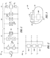
- FIG. 1 illustrates generally an example 100 that can include an electrostatic discharge (ESD) protection circuit 102, such as can be included as a portion of an integrated circuit included in an implantable medical device (e.g., an implantable medical device 300 such as shown in FIG. 3 ).
- the ESD protection circuit 102 can include a first circuit, "Zi ,” such as a first passive circuit, coupled between a control input, "C,” of an active circuit 106, and a first power supply node (e.g., at a voltage V P with respect to a reference, "REF").
- the ESD protection circuit 102 can include a second circuit, "Z 2 ,” such as a second passive circuit, coupled between the control input C of the active circuit 106 and a second power supply node (e.g., at a voltage V N with respect to a reference, "REF").
- V N can be at a DC potential less than Vp, such as at the same potential as REF.
- a combination of the first and second circuits Z ⁇ and Z 2 can provide a sensing circuit.
- the sensing circuit can be configured to trigger the active circuit 106 via the control input C to transition or switch the active circuit 106 from a substantially non-conductive mode (e.g., "cutoff) to a substantially conductive mode (e.g., an "on state"). In this manner, energy such as an ESD voltage transient between Vp and V N can be clamped, shunted, or otherwise dissipated via the active circuit 106.
- the active circuit 106 via a voltage coupled to the control input C, can protect other "downstream" circuitry 104 that can be coupled to one or more of the first or second power supply nodes V P or V N .
- the active circuit 106 can include one or more transistors or drive circuits, such as shown in the illustrative examples of FIGS. 7A through 7B .
- one or more of the first or second circuits Zi or Z 2 can include one or more passive components such as resistors, capacitors, or inductors. Such passive components can be included as a portion of the integrated circuit 100, such as included in an active implantable medical device.
- one or more of Zi or Z 2 can include a capacitor array to enhance a reliability of the ESD protection circuit 102 in the event of a failure of a single capacitor included in the array.
- One or more input or output pads can also be protected from ESD events using a clamp circuit 110 coupled between the pad 108 and a respective power supply node, including a first clamp Di (e.g., a first diode), or a second clamp D 2 (e.g., a second diode).
- a clamp circuit 110 coupled between the pad 108 and a respective power supply node, including a first clamp Di (e.g., a first diode), or a second clamp D 2 (e.g., a second diode).
- a first clamp Di e.g., a first diode
- D 2 e.g., a second diode
- FIG. 2 illustrates generally an example of an array 200A of ESD protection circuits, such as can be included as a portion of an integrated circuit having multiple "power domains."
- a single ESD protection circuit 102 such as shown in FIG. 1 can be used.
- an array 200A of protection circuits can be used.
- a first ESD protection circuit 102A can be coupled between a first supply node Vi and a second supply node V 2 .
- a second ESD protection circuit 102B can be coupled between a second supply node V 2 and a third supply node V 3
- a third ESD protection circuit 102C can be coupled between the third supply node V 3 and the first supply node Vi .
- an ESD transient coupled between respective power supply nodes can still be dissipated or shunted by a respective ESD protection circuit 102 A, 102B, or 102C.
- Such an array 200 A can be scaled appropriately to accommodate more than three power supply nodes, even though only three nodes are shown in the illustrative example of FIG. 3 .
- FIG. 3 illustrates generally an example that can include an active implantable medical device (IMD) 300, such as can include a housing 210 and a dielectric portion 220.
- the IMD 300 can include one or more of an implantable monitor, an implantable pacemaker, an implantable cardioverter-defibrillator (ICD), a cardiac resynchronization therapy (CRT) device, a neurostimulation device, or including one or more other physiologic stimulation, therapy, or monitoring capabilities.
- IMD active implantable medical device
- ICD implantable cardioverter-defibrillator
- CRT cardiac resynchronization therapy
- neurostimulation device or including one or more other physiologic stimulation, therapy, or monitoring capabilities.
- the IMD 300 can be coupled to one or more implantable lead assemblies, including one or more electrodes located distally with respect to the IMD 300.
- one or more intravascular or subcutaneously-implanted leads could be coupled to a circuit 200B included in the IMD 300 via a connector block 250 located on or within the dielectric portion 220 (e.g., the dielectric portion 220 and connector block 250 can comprise a "header").
- One or more of the housing 210 or a fixed electrode 240 can be included as a portion of the IMD 300, such as coupled to the circuit 200B.
- the housing 210 can include a hermetically-sealed conductive housing, such as made of titanium.
- the housing 210 can be electrically connected to the circuit 200B via an electrical coupling 230.
- the circuit 200B can include an ESD protection circuit 102 such as shown in the examples of FIGS. 1 through 2 or elsewhere, to dissipate electrostatically-stored energy that can be inadvertently coupled to the circuit 200B via one or more of the housing 210, the connector block 250, or the electrode 240.
- a reference potential e.g., a "ground” or "REF" potential
- a reference potential can be established corresponding to a potential of one or more of the housing 210, electrode 240, or connector block 250.
- FIG. 4A illustrates generally an example of at least a portion of an ESD protection circuit 400 that can include a sensing circuit having two or more capacitors, such as a first capacitor Cpi and a second capacitor Cp 2 in a parallel configuration, and a resistor Ri .
- a time constant can be established at a control input of an active circuit 106, determined by the sum of the parallel capacitances CPI and Cp 2 multiplied by the resistance of resistor Ri .
- Such a sensing circuit configuration can be a high-pass configuration to couple an electrical transient (e.g., an ESD event) occurring between a first power supply node VPX and a second power supply node VNX to a triggering control input, C.
- an electrical transient e.g., an ESD event
- Cpi or Cp 2 fails in a manner that causes an open circuit, a remaining capacitor can still provide a high-pass configuration, however the time constant can be correspondingly reduced (e.g., shortened in duration corresponding to an increased high-pass cutoff frequency). However, if one of CPI or Cp 2 fails in a manner that causes a short circuit, then the active circuit 106 can be in an undesired continuously-triggered state.
- FIG. 4B illustrates generally an example of at least a portion of an ESD protection circuit 400 that can include a sensing circuit having two or more capacitors, such as a first capacitor Csi and a second capacitor Cs 2 in a series configuration.
- a time constant can be established at a control input of an active circuit 106, determined by one over the sum of the reciprocals of the series capacitances Csi and Cs 2 , multiplied by the resistance of resistor Ri .
- Such a sensing circuit configuration can also provide a high-pass configuration, as in the illustrative example of FIG. 4A .
- a remaining capacitor can still provide a high-pass configuration, with a corresponding increase in the time constant (e.g., the time constant can be lengthened, decreasing a high-pass cut-off frequency).
- the originally-specified high-pass frequency range can be preserved, at the cost that lower frequencies may also trigger the control input in the event of a single capacitor failure. If one of Csi or Cs 2 fails in a manner that causes an open circuit, then the sensing circuit can become inhibited from triggering the control input of the active circuit 106.
- FIG. 4C illustrates generally an example of at least a portion of an ESD protection circuit 400C that can include a sensing circuit having two or more capacitors in a series and parallel (e.g., a series-parallel) configuration.
- a capacitor array including both series and parallel capacitors can provide redundancy for both short-circuit and open-circuit failure modes.
- the capacitors in the array such as including first through fourth capacitors, Ci through C 4 (or one or more other configurations), can each include a specified capacitance value or working voltage rating.
- the working voltage rating can be de-rated corresponding to a number of series "rungs" in the array. For example, a specified single (or multiple) short-circuit failure condition need not cause a voltage across a respective capacitor to exceed its corresponding working voltage rating.
- a voltage difference between a first power supply node V PX and a second power supply node V N x can be about 12 volts.
- a working voltage range for each capacitor can be specified as in excess of 12 volts.
- a voltage of about 6 volts would be dropped across each capacitor during ambulatory operation (e.g., in a non-fault operational scenario).
- 12 volts may be applied across remaining capacitors that are not short-circuited by the failure.
- Capacitor C 4 would be bypassed by the short-circuit failure of C 2 .
- Capacitors Ci and C 3 can still operate reliably, being rated for at least 12V in this illustrative example. Redundancy can also be provided such as by using different capacitor dielectric materials or capacitor configurations for respective capacitors, as shown in the illustrative example of FIG. 6 .
- FIG. 5 illustrates generally an example of at least a portion of a sensing circuit that can be included as a portion of an ESD protection circuit, that can include one or more conductive features Mi through M 4 , an array of capacitors, such as including a first capacitor CAI or a second capacitor CA2 , or an array of resistors, such as a first resistor Ri or a second resistor R 2 .
- the conductive features Mi through M 4 can include metal or one or more other conductive materials that can be used to select a desired capacitance or resistance, such as using a metal-only mask adjustment before or during fabrication of an integrated circuit.
- a desired time constant (as discussed in the examples of FIGS. 1, 2 , or 4A through 4C ) can be selected for the sensing circuit by including or omitting various conductive (e.g., metallization layer) features Mi through M 4 , without requiring modification of other layers of an integrated circuit.
- FIG. 6 illustrates generally a section view of at least a portion of an integrated circuit 600 that can include two or more capacitors, or a field-effect transistor (FET) device, that can be included as a portion of an implantable medical device.
- the FET device 628 can be included as a portion of the active circuit 106 as discussed in the examples of above and elsewhere.
- the FET device 628 can include respective first and second well regions 604A and 604B, including a conductivity type opposite the type of the substrate 602 (or, in an example, opposite the conductivity type of a larger well or epitaxially-grown region surrounding the FET device 628).
- Such well regions 604 A and 604B can be specified as source or drain regions.
- a gate dielectric 616 can be formed, such as slightly laterally overlapping with a portion of the well regions 604A and 604B.
- a conductive terminal such as a metal or polysilicon terminal can be formed on the gate 616 dielectric to provide a gate terminal 614.
- One or more of the well regions 604A and 604B, or the gate terminal 614 can be electrically coupled to other portions of the integrated circuit 600, such as to provide an ESD protection circuit as discussed in other examples above or below.
- a first capacitor can include a poly-poly capacitor 630, comprising a first polysilicon terminal 612 (or including one or more other conductive materials) grown or deposited on a dielectric layer 608 (e.g., silicon dioxide (Si0 2 ) or including one or more other materials).
- a dielectric layer 608 e.g., silicon dioxide (Si0 2 ) or including one or more other materials.
- a capacitor dielectric material 610 can be formed on the first polysilicon terminal 612, using a chemical vapor deposition technique, a spin-on technique, a sputtering technique, or using one or more other techniques.
- a second polysilicon terminal 606 can be formed, for example, opposite (e.g., above, as shown in FIG. 6 ) the first polysilicon terminal 612, with the capacitor dielectric material 610 separating the first and second polysilicon terminals 612 and 606.
- a second capacitor can include a dielectric-on-monocrystalline-silicon configuration 626.
- the substrate 602 can include a first conductivity type, such as a positive (p-type) doping impurity.
- a well region 624 can include an n-type or p-type doping impurity.
- the second capacitor can include a thermally-grown or "native" oxide layer 620 formed on the substrate 602, such as in a manner similar to a gate dielectric 616 formed as a portion of the FET device 628.
- the second capacitor including the dielectric-on-monocrystalline-silicon configuration 626 can include respective first and second well regions 604C and 604D, such as including an n-type or p-type doping impurity.
- the dielectric-on-monocrystalline-silicon configuration 626 can be fabricated as an enhancement-mode or depletion-mode device, and a capacitance can be dependent, such as nonlinearly dependent, on a polarity and a magnitude of a voltage applied between the substrate 602 and a terminal 618 of the dielectric-on-monocrystalline-silicon configuration 626.
- An array of capacitors can be formed, such as via using one or more capacitors including the poly-poly capacitor 630 configuration, or the dielectric-on-monocrystalline-silicon configuration 626, or using one or more other configurations.
- One or more conductive layers e.g., one or metallization layers
- One or more conductive layers can be formed or deposited to provide electrical interconnections between one or more of the poly-poly capacitor 630, the FET device 628, or the second capacitor in the dielectric-on-monocrystalline-silicon configuration 626.
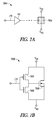
- FIG. 7A illustrates generally an example of at least a portion of an ESD protection circuit 700A that can include an active circuit 706A comprising a shunt device and a drive circuit 760.
- the active circuit 106 of FIGS. 1 or 2 need not be a single device.
- a FET device 628 as shown in FIG. 6 can be specified to reliably shunt multiple ESD events without degradation.
- One or more other active circuits can be used, such as one or more of a bipolar junction transistor, a junction FET, or an IGBT.
- one or more drive circuits can be used, such as coupled to a control input (e.g., a gate) of the active circuit 706A to reliably trigger the active circuit 706A into a conductive mode during an ESD event.
- a drive circuit can include one or more transistors, such as a complementary transistor pair as shown in the illustrative example of FIG. 7B .
- Other configurations can be used, such as one or more inverting or non-inverting drive configurations.
- an input 170 can trigger the active circuit 706A in response to voltage transition from a higher voltage to a lower voltage.
- the active circuit 706A e.g., the shunt device
- the active circuit 706A can be in a nonconducting mode during ambulatory operation and can be switched into a conducting mode and held in such a conducting mode by the drive circuit 760 for at least a duration of an ESD event.
- FIG. 7B illustrates generally an example of at least a portion of ESD protection circuit that can include a FET shunt device 706B and a complementary FET drive circuit including a first FET device 760A having a first conductivity type (e.g., a PMOS device) and a second FET device 760B having a second conductivity type (e.g., an NMOS device).
- the drive circuit can include an inverting configuration, triggering the shunt device 706B in response to a voltage transition from a higher voltage to a lower voltage passing through a specified voltage threshold.
- FIG. 8 illustrates generally a technique 800, such as a method, that can include forming a housing of an implantable medical device (IMD), at 802, and forming circuits that can be placed in the housing, such as a portion of an ESD protection circuit discussed in the examples of FIGS. 1, 2, 3 , 4A through 4C , 5, 6 , 7A through 7B , or elsewhere.
- IMD implantable medical device
- an active circuit can be formed, including one or more transistors, the active circuit configured to selectively electrically couple a first power supply node to a second power supply node in response to a control signal received via a control input.
- a first passive circuit can be formed, the first passive circuit electrically coupled between the first power supply node and the control input of the active circuit.
- a second passive circuit can be formed. The second passive circuit can be electrically coupled between the second power supply node and the control input of the active circuit.
- at least one of forming the first or second passive circuits includes forming an array of capacitors in a series configuration, a parallel configuration, or a combination of series and parallel configurations.
- the first and second passive circuits can be configured to establish a specified time constant, and, in response to an applied ESD, the first and second passive circuits can be configured to provide the control signal to the control input using the specified time constant, and the active circuit can be configured to switch from a substantially non-conductive mode to a substantially conductive mode in response to the control signal to provide a shunt path for the applied ESD between the first and second power supply nodes.
- present inventors also contemplate examples in which only those elements shown or described are provided. Moreover, the present inventors also contemplate examples using any combination or permutation of those elements shown or described (or one or more aspects thereof), either with respect to a particular example (or one or more aspects thereof), or with respect to other examples (or one or more aspects thereof) shown or described herein.
- Method examples described herein can be machine or computer-implemented at least in part. Some examples can include a computer-readable medium or machine-readable medium encoded with instructions operable to configure an electronic device to perform methods as described in the above examples.
- An implementation of such methods can include code, such as microcode, assembly language code, a higher-level language code, or the like. Such code can include computer readable instructions for performing various methods. The code may form portions of computer program products. Further, in an example, the code can be tangibly stored on one or more volatile, non-transitory, or non-volatile tangible computer-readable media, such as during execution or at other times.
- Examples of these tangible computer-readable media can include, but are not limited to, hard disks, removable magnetic disks, removable optical disks (e.g., compact disks and digital video disks), magnetic cassettes, memory cards or sticks, random access memories (RAMs), read only memories (ROMs), and the like.
- Example 6 can include, or can optionally be combined with the subject matter of Example 5, to optionally include a second capacitor included in one or more of the first or second passive circuits comprising a capacitor dielectric located between polysilicon regions of an integrated circuit.
- Example 7 can include, or can optionally be combined with the subject matter of one or any combination of Examples 1 through 6 to optionally include an active circuit comprising a shunt Field Effect Transistor (FET) configured to the couple the first power supply node to the second power supply node.
- FET Field Effect Transistor
- Example 8 can include, or can optionally be combined with the subject matter of Example 7, to optionally include an active circuit comprising a drive circuit coupled to a gate of the shunt FET, the control input comprising an input of the drive circuit.
- Example 9 can include, or can optionally be combined with the subject matter of Example 8, to optionally include a drive circuit comprising a complementary transistor pair.
- Example 10 can include, or can optionally be combined with the subject matter of one or any combination of Examples 1 through 9 to optionally include a first power supply node comprising a first DC supply voltage, the second power supply node comprising a second DC supply voltage, the first DC supply voltage positive in polarity with respect to the second DC supply voltage.
- Example 11 can include, or can optionally be combined with the subject matter of Example 10, to optionally include a second power supply node comprising a reference node.
- Example 12 can include, or can optionally be combined with the subject matter of Example 11, to optionally include a conductive housing, the reference node electrically coupled to the housing.
- Example 13 can include, or can optionally be combined with the subject matter of Example 12, to optionally include a dielectric portion coupled to the housing, the dielectric portion including an electrode on or within the dielectric portion, the integrated circuit comprising a bond pad, the electrode electrically coupled to the bond pad; the integrated circuit comprising at least one ESD clamp circuit between the bond pad an at least one power supply node.
- Example 14 can include, or can optionally be combined with the subject matter of one or any combination of Examples 1 through 13 to include, subject matter (e.g., an apparatus, a method, a means for performing acts, or a machine readable medium including instructions that, when performed by the machine, that can cause the machine to perform acts), which can include an implantable medical device, comprising a housing, an integrated circuit included in the housing, the integrated circuit comprising an electrostatic discharge (ESD) protection circuit including an active circuit configured to selectively electrically couple a first power supply node to a second power supply node in response to a control signal received via a control input, a first passive circuit electrically coupled between the first power supply node and the control input of the active circuit, a second passive circuit electrically coupled between the second power supply node and the control input of the active circuit, the first passive circuit including an array of capacitors in a series and parallel configuration, the second passive circuit including a resistor, the first and second passive circuits configured to establish a specified time constant, and, in response to an applied E
- Example 15 can include, or can optionally be combined with the subject matter of one or any combination of Examples 1 through 14 to include, subject matter (e.g., an apparatus, a method, a means for performing acts, or a machine readable medium including instructions that, when performed by the machine, that can cause the machine to perform acts), such as can include a method for providing electrostatic discharge (ESD) protection in an implantable medical device, the method comprising forming a housing, forming an integrated circuit in the housing, the integrated circuit including an electrostatic discharge (ESD) protection circuit, the forming the integrated circuit comprising forming an active circuit configured to selectively electrically couple a first power supply node to a second power supply node in response to a control signal received via a control input, forming a first passive circuit electrically coupled between the first power supply node and the control input of the active circuit, forming a second passive circuit electrically coupled between the second power supply node and the control input of the active circuit, at least one of forming the first or second passive circuits including forming an array of
- Example 16 can include, or can optionally be combined with the subject matter of Example 15, to optionally include forming the first passive circuit including forming an array of capacitors in a series and parallel configuration, and forming the second passive circuit includes forming a resistor.
- Example 17 can include, or can optionally be combined with the subject matter of one or any combination of Examples 15 or 16 to optionally include forming at least one of the first or second passive circuits including forming an array of at least two capacitors in a series configuration.
- Example 18 can include, or can optionally be combined with the subject matter of one or any combination of Examples 15 through 17 to optionally include forming at least one of the first or second passive circuits including forming an array of at least two capacitors in a parallel configuration.
- Example 19 can include, or can optionally be combined with the subject matter of one or any combination of Examples 15 through 18 to optionally include forming a first capacitor included in one or more of the first or second passive circuits including forming a capacitor dielectric comprising a dielectric on a monocrystalline region of an integrated circuit substrate.
- Example 20 can include, or can optionally be combined with the subject matter of one or any combination of Examples 15 through 19 to optionally include forming a second capacitor included in one or more of the first or second passive circuits including forming a capacitor dielectric located between polysilicon regions of an integrated circuit.
- Method examples described herein can be machine or computer-implemented at least in part. Some examples can include a computer-readable medium or machine-readable medium encoded with instructions operable to configure an electronic device to perform methods as described in the above examples.
- An implementation of such methods can include code, such as microcode, assembly language code, a higher-level language code, or the like. Such code can include computer readable instructions for performing various methods. The code may form portions of computer program products. Further, in an example, the code can be tangibly stored on one or more volatile, non-transitory, or non-volatile tangible computer-readable media, such as during execution or at other times.
- Examples of these tangible computer-readable media can include, but are not limited to, hard disks, removable magnetic disks, removable optical disks (e.g., compact disks and digital video disks), magnetic cassettes, memory cards or sticks, random access memories (RAMs), read only memories (ROMs), and the like.
Landscapes
- Health & Medical Sciences (AREA)
- Engineering & Computer Science (AREA)
- Nuclear Medicine, Radiotherapy & Molecular Imaging (AREA)
- Radiology & Medical Imaging (AREA)
- Physics & Mathematics (AREA)
- Cardiology (AREA)
- Heart & Thoracic Surgery (AREA)
- Biomedical Technology (AREA)
- Microelectronics & Electronic Packaging (AREA)
- Electromagnetism (AREA)
- Life Sciences & Earth Sciences (AREA)
- Animal Behavior & Ethology (AREA)
- General Health & Medical Sciences (AREA)
- Public Health (AREA)
- Veterinary Medicine (AREA)
- Semiconductor Integrated Circuits (AREA)
- Metal-Oxide And Bipolar Metal-Oxide Semiconductor Integrated Circuits (AREA)
- Electrotherapy Devices (AREA)
Description
- Electronic integrated circuits can include many devices, such as thousands or even millions of transistors, resistors, capacitors, interconnections, or other devices. Electrostatically-stored energy, when discharged, can damage integrated circuits such as via electrically overstressing devices included in such circuits. For example, Field Effect Transistors (FETs) or capacitors can be particularly sensitive to ESD events, such as due to a vulnerability of an oxide or other dielectric layer to such ESD events. ESD can occur during manufacturing, during handling, during distribution, during end use of integrated circuits, or in other cases. Equipment, packaging, or humans can electrostatically accumulate and store damaging amounts of such charge, which can then be inadvertently discharged via a pathway through or near the integrated circuit. In one approach, precautionary handling measures can be taken to dissipate electrostatically-stored energy, such as using "grounded" or conductive electrical workstations or packaging, but such measures generally only reduce rather than eliminate the threat of ESD-induced damage to integrated circuits.
- Ortmans et al. have published an article entitled "A retina stimulator ASIC with 232 electrodes, custom ESD protection and active charge balancing," in the proceedings of the 2006 IEEE International Symposium on Circuits and Systems, page 4pp (DOI: 10.1109/ISCAS.2006.1693342) a system and design of a retina stimulator with 232 electrodes in a 0.35mum HVCMOS technology. The requirements are outlined and the system architecture is explained. The stimulator provides more than plusmn15 V output swing, features full custom ESD protection at the electrodes and is fully testable. To prevent electrolysis through dc-currents, a new active charge balancer is implemented. Measurement results confirm the approach
- Generally, an integrated circuit can include one or more bond pads, such as to provide an electrical and mechanical connection to one or more conductors included as a portion of an integrated circuit device package. Such bond pads can be referred to as inputs or outputs (I/Os) and can be coupled to an electrostatic discharge (ESD) clamp circuit included as a portion of the integrated circuit or external to the integrated circuit, such as coupled between a bond pad node and one or more power supply nodes. Such a clamp circuit can, for example, limit an applied voltage applied between a bond pad and a supply node to within a specified voltage range.
- In one approach, such as in addition to I/O protection, one or more ESD protection circuits can be included as a portion of the integrated circuit, such as between two or more power supply nodes. An ESD protection circuit can include an active device, such as a transistor, and a sensing circuit, such as including a resistor and a capacitor. Such a sensing circuit can be coupled to a control input of the active device, such as to trigger the active device so that the active device becomes conductive for a duration of an ESD event. For example, such an active device can provide energy dissipation or a shunt pathway for ESD energy, such as between the two or more power supply nodes. An ESD-triggered shunt pathway can prevent electrical overstress of other circuitry coupled to the power supply nodes. In an example of an integrated circuit having multiple power supply nodes (e.g., a "multiple power domain" example), an array of ESD protection circuits can be used to reduce or inhibit electrical overstress, such as due to ESD-induced voltage or other electrical transient applied between respective power supply nodes.
- The present inventors have recognized, among other things, that a configuration of a sensing circuit included as a portion of an ESD protection circuit can affect a reliability of the ESD protection circuit. For example, a sensing circuit including a single capacitor can fail, such as due at least in part to a time-dependent dielectric breakdown (TDDB) of the capacitor. TDDB can make the failing capacitor behave as an electrical short circuit. The present inventors have also recognized that a rate of such time-dependent dielectric breakdown can be influenced by an operating voltage (e.g., a "working voltage") applied across a capacitor. For example, a higher working voltage can cause TDDB to occur more rapidly over a lifetime of the capacitor. In an implantable application, including an implantable medical device having one or more integrated circuits, a failure of an ESD protection circuit due to TDDB can cause unwanted effects such as premature battery depletion of the implantable device.
- Accordingly, the present inventors have recognized, among other things, that an array including two or more capacitors can be included as a portion of an ESD protection circuit, such as comprising a sensing circuit including two or more capacitors in a series configuration, a parallel configuration, or a combination of series and parallel configurations. Such series, parallel, or series-parallel capacitor configurations can provide redundancy, such as providing reliable ESD protection circuit operation in the presence of one or more of a short circuit capacitor failure (e.g., due to TDDB), an open circuit capacitor failure (e.g., due to an interconnect failure), a "leaky" or "lossy" capacitor failure (e.g., where a capacitor equivalent series resistance or leakage resistance is outside of a specified range), or one or more other failure modes.
- This overview is intended to provide an overview of subject matter of the present patent application. It is not intended to provide an exclusive or exhaustive explanation of the invention. The detailed description is included to provide further information about the present patent application.
- In the drawings, which are not necessarily drawn to scale, like numerals may describe similar components in different views. Like numerals having different letter suffixes may represent different instances of similar components. The drawings illustrate generally, by way of example, but not by way of limitation, various embodiments discussed in the present document.
-
FIG. 1 illustrates generally an example that can include an electrostatic discharge (ESD) protection circuit, such as can be included as a portion of an integrated circuit included in an implantable medical device. -
FIG. 2 illustrates generally an example of an array of ESD protection circuits, such as can be included as a portion of an integrated circuit having multiple "power domains." -
FIG. 3 illustrates generally an example that can include an implantable medical device, such as can include a housing and a dielectric header assembly. -
FIG. 4A illustrates generally an example of at least a portion of an ESD protection circuit including a sensing circuit having two or more capacitors in a parallel configuration. -
FIG. 4B illustrates generally an example of at least a portion of an ESD protection circuit including a sensing circuit having two or more capacitors in a series configuration. -
FIG. 4C illustrates generally an example of at least a portion of an ESD protection circuit including a sensing circuit having two or more capacitors in series-parallel configuration. -
FIG. 5 illustrates generally an example of at least a portion of a sensing circuit that can be included as a portion of an ESD protection circuit, such as can include one or more metal features that can be used to select a desired capacitance or resistance, such as using a metal-only mask adjustment. -
FIG. 6 illustrates generally a section view of at least a portion of an integrated circuit that can include two or more capacitor devices, and a field-effect transistor (FET) device, such as can be included as a portion of an implantable medical device. -
FIG. 7A illustrates generally an example of at least portion of an ESD protection circuit that can include an active circuit comprising a shunt device and a drive circuit. -
FIG. 7B illustrates generally an example of at least a portion of ESD protection circuit that can include a FET shunt device, and a complementary FET drive circuit. -
FIG. 8 illustrates generally a technique, such as a method, that can include forming an integrated circuit such as for an implantable medical device. -
FIG. 1 illustrates generally an example 100 that can include an electrostatic discharge (ESD)protection circuit 102, such as can be included as a portion of an integrated circuit included in an implantable medical device (e.g., an implantablemedical device 300 such as shown inFIG. 3 ). In the example ofFIG. 1 , theESD protection circuit 102 can include a first circuit, "Zi ," such as a first passive circuit, coupled between a control input, "C," of anactive circuit 106, and a first power supply node (e.g., at a voltage VP with respect to a
reference, "REF"). TheESD protection circuit 102 can include a second circuit, "Z2," such as a second passive circuit, coupled between the control input C of theactive circuit 106 and a second power supply node (e.g., at a voltage VN with respect to a reference, "REF"). In an example, VN can be at a DC potential less than Vp, such as at the same potential as REF. - In an example, a combination of the first and second circuits Z\ and Z2 can provide a sensing circuit. The sensing circuit can be configured to trigger the
active circuit 106 via the control input C to transition or switch theactive circuit 106 from a substantially non-conductive mode (e.g., "cutoff) to a substantially conductive mode (e.g., an "on state"). In this manner, energy such as an ESD voltage transient between Vp and VN can be clamped, shunted, or otherwise dissipated via theactive circuit 106. When triggered, theactive circuit 106 via a voltage coupled to the control input C, can protect other "downstream"circuitry 104 that can be coupled to one or more of the first or second power supply nodes VP or VN. In an example, theactive circuit 106 can include one or more transistors or drive circuits, such as shown in the illustrative examples ofFIGS. 7A through 7B . - In an example, one or more of the first or second circuits Zi or Z2 can include one or more passive components such as resistors, capacitors, or inductors. Such passive components can be included as a portion of the
integrated circuit 100, such as included in an active implantable medical device. For example, as shown inFIGS. 4A through 4C , orFIG. 5 , one or more of Zi or Z2 can include a capacitor array to enhance a reliability of theESD protection circuit 102 in the event of a failure of a single capacitor included in the array. - One or more input or output pads, such as a
pad 108, can also be protected from ESD events using aclamp circuit 110 coupled between thepad 108 and a respective power supply node, including a first clamp Di (e.g., a first diode), or a second clamp D2 (e.g., a second diode). Such clamp circuits can be included in addition to the power supply "rail" protection offered by theESD protection circuit 102.FIG. 2 illustrates generally an example of anarray 200A of ESD protection circuits, such as can be included as a portion of an integrated circuit having multiple "power domains." Generally, if two power supply nodes (e.g., a positive voltage and a reference) are used, then a singleESD protection circuit 102 such as shown inFIG. 1 can be used. If more than two power supply nodes are used (e.g., such as for supplying respective "power domains" in an analog or mixed-mode integrated circuit), anarray 200A of protection circuits can be used. For example, a firstESD protection circuit 102A can be coupled between a first supply node Vi and a second supply node V2. A secondESD protection circuit 102B can be coupled between a second supply node V2 and a third supply node V3, and a thirdESD protection circuit 102C can be coupled between the third supply node V3 and the first supply node Vi . In this manner, an ESD transient coupled between respective power supply nodes (or in common with two power supply nodes) can still be dissipated or shunted by a respectiveESD protection circuit array 200 A can be scaled appropriately to accommodate more than three power supply nodes, even though only three nodes are shown in the illustrative example ofFIG. 3 . -
FIG. 3 illustrates generally an example that can include an active implantable medical device (IMD) 300, such as can include ahousing 210 and adielectric portion 220. TheIMD 300 can include one or more of an implantable monitor, an implantable pacemaker, an implantable cardioverter-defibrillator (ICD), a cardiac resynchronization therapy (CRT) device, a neurostimulation device, or including one or more other physiologic stimulation, therapy, or monitoring capabilities. - In an example, the
IMD 300 can be coupled to one or more implantable lead assemblies, including one or more electrodes located distally with respect to theIMD 300. For example, one or more intravascular or subcutaneously-implanted leads could be coupled to acircuit 200B included in theIMD 300 via aconnector block 250 located on or within the dielectric portion 220 (e.g., thedielectric portion 220 andconnector block 250 can comprise a "header"). One or more of thehousing 210 or a fixedelectrode 240 can be included as a portion of theIMD 300, such as coupled to thecircuit 200B. Thehousing 210 can include a hermetically-sealed conductive housing, such as made of titanium. Thehousing 210 can be electrically connected to thecircuit 200B via anelectrical coupling 230. Thecircuit 200B can include anESD protection circuit 102 such as shown in the examples ofFIGS. 1 through 2 or elsewhere, to dissipate electrostatically-stored energy that can be inadvertently coupled to thecircuit 200B via one or more of thehousing 210, theconnector block 250, or theelectrode 240. In an example, a reference potential (e.g., a "ground" or "REF" potential) can be established corresponding to a potential of one or more of thehousing 210,electrode 240, orconnector block 250. -
FIG. 4A illustrates generally an example of at least a portion of an ESD protection circuit 400 that can include a sensing circuit having two or more capacitors, such as a first capacitor Cpi and a second capacitor Cp2 in a parallel configuration, and a resistor Ri . InFIG. 4A , a time constant can be established at a control input of anactive circuit 106, determined by the sum of the parallel capacitances CPI and Cp2 multiplied by the resistance of resistor Ri . Such a sensing circuit configuration can be a high-pass configuration to couple an electrical transient (e.g., an ESD event) occurring between a first power supply node VPX and a second power supply node VNX to a triggering control input, C. If one of Cpi or Cp2 fails in a manner that causes an open circuit, a remaining capacitor can still provide a high-pass configuration, however the time constant can be correspondingly reduced (e.g., shortened in duration corresponding to an increased high-pass cutoff frequency). However, if one of CPI or Cp2 fails in a manner that causes a short circuit, then theactive circuit 106 can be in an undesired continuously-triggered state. -
FIG. 4B illustrates generally an example of at least a portion of an ESD protection circuit 400 that can include a sensing circuit having two or more capacitors, such as a first capacitor Csi and a second capacitor Cs2 in a series configuration. InFIG. 4B , a time constant can be established at a control input of anactive circuit 106, determined by one over the sum of the reciprocals of the series capacitances Csi and Cs2, multiplied by the resistance of resistor Ri . Such a sensing circuit configuration can also provide a high-pass configuration, as in the illustrative example ofFIG. 4A . If one of Csi or Cs2 fails in a manner that causes a short circuit or a low resistance, such as due to TDDB, a remaining capacitor can still provide a high-pass configuration, with a corresponding increase in the time constant (e.g., the time constant can be lengthened, decreasing a high-pass cut-off frequency). In this manner, for short-circuit or low-resistance (e.g. high leakage) capacitor failure modes, the originally-specified high-pass frequency range can be preserved, at the cost that lower frequencies may also trigger the control input in the event of a single capacitor failure. If one of Csi or Cs2 fails in a manner that causes an open circuit, then the sensing circuit can become inhibited from triggering the control input of theactive circuit 106. -
FIG. 4C illustrates generally an example of at least a portion of anESD protection circuit 400C that can include a sensing circuit having two or more capacitors in a series and parallel (e.g., a series-parallel) configuration. The present inventors have recognized, among other things, that a capacitor array including both series and parallel capacitors can provide redundancy for both short-circuit and open-circuit failure modes. In an example, the capacitors in the array, such as including first through fourth capacitors, Ci through C4 (or one or more other configurations), can each include a specified capacitance value or working voltage rating. The working voltage rating can be de-rated corresponding to a number of series "rungs" in the array. For example, a specified single (or multiple) short-circuit failure condition need not cause a voltage across a respective capacitor to exceed its corresponding working voltage rating. - In an illustrative example, a voltage difference between a first power supply node VPX and a second power supply node VNx can be about 12 volts. A working voltage range for each capacitor can be specified as in excess of 12 volts. In the example of
FIG. 4C , assuming roughly equal series resistances for the capacitors Ci through C4, a voltage of about 6 volts would be dropped across each capacitor during ambulatory operation (e.g., in a non-fault operational scenario). In the event of a single short-circuit failure, 12 volts may be applied across remaining capacitors that are not short-circuited by the failure. For example, if capacitor C2 failed and became short-circuited, the voltage difference between VPX and VNX would be applied across capacitors Ci and C3 (e.g., about 12V would be applied across capacitors Ci and C3, rather than 6V). Capacitor C4 would be bypassed by the short-circuit failure of C2. Capacitors Ci and C3 can still operate reliably, being rated for at least 12V in this illustrative example. Redundancy can also be provided such as by using different capacitor dielectric materials or capacitor configurations for respective capacitors, as shown in the illustrative example ofFIG. 6 . -
FIG. 5 illustrates generally an example of at least a portion of a sensing circuit that can be included as a portion of an ESD protection circuit, that can include one or more conductive features Mi through M4, an array of capacitors, such as including a first capacitor CAI or a second capacitor CA2 , or an array of resistors, such as a first resistor Ri or a second resistor R2. The conductive features Mi through M4 can include metal or one or more other conductive materials that can be used to select a desired capacitance or resistance, such as using a metal-only mask adjustment before or during fabrication of an integrated circuit. For example, a desired time constant (as discussed in the examples ofFIGS. 1, 2 , or4A through 4C ) can be selected for the sensing circuit by including or omitting various conductive (e.g., metallization layer) features Mi through M4, without requiring modification of other layers of an integrated circuit. -
FIG. 6 illustrates generally a section view of at least a portion of an integrated circuit 600 that can include two or more capacitors, or a field-effect transistor (FET) device, that can be included as a portion of an implantable medical device. TheFET device 628 can be included as a portion of theactive circuit 106 as discussed in the examples of above and elsewhere. For example, theFET device 628 can include respective first andsecond well regions well regions gate dielectric 616 can be formed, such as slightly laterally overlapping with a portion of thewell regions gate 616 dielectric to provide agate terminal 614. One or more of thewell regions gate terminal 614 can be electrically coupled to other portions of the integrated circuit 600, such as to provide an ESD protection circuit as discussed in other examples above or below. - In the illustrative example of
FIG. 6 , a first capacitor can include a poly-poly capacitor 630, comprising a first polysilicon terminal 612 (or including one or more other conductive materials) grown or deposited on a dielectric layer 608 (e.g., silicon dioxide (Si02) or including one or more other materials). Such adielectric layer 608 can be located upon or can comprise a portion of asemiconductor substrate 602. Acapacitor dielectric material 610 can be formed on thefirst polysilicon terminal 612, using a chemical vapor deposition technique, a spin-on technique, a sputtering technique, or using one or more other techniques. Asecond polysilicon terminal 606 can be formed, for example, opposite (e.g., above, as shown inFIG. 6 ) thefirst polysilicon terminal 612, with thecapacitor dielectric material 610 separating the first andsecond polysilicon terminals - A second capacitor can include a dielectric-on-monocrystalline-
silicon configuration 626. For example, thesubstrate 602 can include a first conductivity type, such as a positive (p-type) doping impurity. Awell region 624 can include an n-type or p-type doping impurity. The second capacitor can include a thermally-grown or "native"oxide layer 620 formed on thesubstrate 602, such as in a manner similar to agate dielectric 616 formed as a portion of theFET device 628. The second capacitor including the dielectric-on-monocrystalline-silicon configuration 626 can include respective first and secondwell regions oxide layer 620 on a monocrystalline region can reduce or inhibit defect propagation into theoxide layer 620, providing reduced susceptibility to TDDB as compared to the poly-poly capacitor 630. Unlike the poly-poly capacitor 630, the dielectric-on-monocrystalline-silicon configuration 626 can be fabricated as an enhancement-mode or depletion-mode device, and a capacitance can be dependent, such as nonlinearly dependent, on a polarity and a magnitude of a voltage applied between thesubstrate 602 and aterminal 618 of the dielectric-on-monocrystalline-silicon configuration 626. - An array of capacitors can be formed, such as via using one or more capacitors including the poly-
poly capacitor 630 configuration, or the dielectric-on-monocrystalline-silicon configuration 626, or using one or more other configurations. One or more conductive layers (e.g., one or metallization layers) can be formed or deposited to provide electrical interconnections between one or more of the poly-poly capacitor 630, theFET device 628, or the second capacitor in the dielectric-on-monocrystalline-silicon configuration 626. -
FIG. 7A illustrates generally an example of at least a portion of anESD protection circuit 700A that can include anactive circuit 706A comprising a shunt device and adrive circuit 760. As discussed in other examples above, theactive circuit 106 ofFIGS. 1 or 2 need not be a single device. For example, aFET device 628 as shown inFIG. 6 can be specified to reliably shunt multiple ESD events without degradation. One or more other active circuits can be used, such as one or more of a bipolar junction transistor, a junction FET, or an IGBT. - Accordingly, in an example, one or more drive circuits can be used, such as coupled to a control input (e.g., a gate) of the
active circuit 706A to reliably trigger theactive circuit 706A into a conductive mode during an ESD event. Such a drive circuit can include one or more transistors, such as a complementary transistor pair as shown in the illustrative example ofFIG. 7B . Other configurations can be used, such as one or more inverting or non-inverting drive configurations. For example, in an inverting configuration, aninput 170 can trigger theactive circuit 706A in response to voltage transition from a higher voltage to a lower voltage. In such an inverting example, the locations of the capacitors in the examples ofFIGS. 4A through 4C orFIG. 5 would be exchanged with resistors, and the locations with resistors would be exchanged with capacitors. Generally, whether thedrive circuit 760 is inverting or non-inverting, theactive circuit 706A (e.g., the shunt device) can be in a nonconducting mode during ambulatory operation and can be switched into a conducting mode and held in such a conducting mode by thedrive circuit 760 for at least a duration of an ESD event. -
FIG. 7B illustrates generally an example of at least a portion of ESD protection circuit that can include aFET shunt device 706B and a complementary FET drive circuit including afirst FET device 760A having a first conductivity type (e.g., a PMOS device) and asecond FET device 760B having a second conductivity type (e.g., an NMOS device). In the example ofFIG. 7B , the drive circuit can include an inverting configuration, triggering theshunt device 706B in response to a voltage transition from a higher voltage to a lower voltage passing through a specified voltage threshold. -
FIG. 8 illustrates generally atechnique 800, such as a method, that can include forming a housing of an implantable medical device (IMD), at 802, and forming circuits that can be placed in the housing, such as a portion of an ESD protection circuit discussed in the examples ofFIGS. 1, 2, 3 ,4A through 4C ,5, 6 ,7A through 7B , or elsewhere. For example, at 804, an active circuit can be formed, including one or more transistors, the active circuit configured to selectively electrically couple a first power supply node to a second power supply node in response to a control signal received via a control input. - At 806, a first passive circuit can be formed, the first passive circuit electrically coupled between the first power supply node and the control input of the active circuit. At 808, a second passive circuit can be formed. The second passive circuit can be electrically coupled between the second power supply node and the control input of the active circuit. In an example, at least one of forming the first or second passive circuits includes forming an array of capacitors in a series configuration, a parallel configuration, or a combination of series and parallel configurations. In an example, the first and second passive circuits can be configured to establish a specified time constant, and, in response to an applied ESD, the first and second passive circuits can be configured to provide the control signal to the control input using the specified time constant, and the active circuit can be configured to switch from a substantially non-conductive mode to a substantially conductive mode in response to the control signal to provide a shunt path for the applied ESD between the first and second power supply nodes.
- The above detailed description includes references to the accompanying drawings, which form a part of the detailed description. The drawings show, by way of illustration, specific embodiments in which the invention can be practiced. These embodiments are also referred to herein as "examples." Such examples can include elements in addition to those shown or described.
- However, the present inventors also contemplate examples in which only those elements shown or described are provided. Moreover, the present inventors also contemplate examples using any combination or permutation of those elements shown or described (or one or more aspects thereof), either with respect to a particular example (or one or more aspects thereof), or with respect to other examples (or one or more aspects thereof) shown or described herein.
- In the event of inconsistent usages between this document and any documents so incorporated by reference, the usage in this document controls.
- In this document, the terms "a" or "an" are used, as is common in patent documents, to include one or more than one, independent of any other instances or usages of "at least one" or "one or more." In this document, the term "or" is used to refer to a nonexclusive or, such that "A or B" includes "A but not B," "B but not A," and "A and B," unless otherwise indicated. In this document, the terms "including" and "in which" are used as the plain-English equivalents of the respective terms "comprising" and "wherein." Also, in the following claims, the terms "including" and "comprising" are open-ended, that is, a system, device, article, composition, formulation, or process that includes elements in addition to those listed after such a term in a claim are still deemed to fall within the scope of that claim. Moreover, in the following claims, the terms "first," "second," and "third," etc. are used merely as labels, and are not intended to impose numerical requirements on their objects.
- Method examples described herein can be machine or computer-implemented at least in part. Some examples can include a computer-readable medium or machine-readable medium encoded with instructions operable to configure an electronic device to perform methods as described in the above examples. An implementation of such methods can include code, such as microcode, assembly language code, a higher-level language code, or the like. Such code can include computer readable instructions for performing various methods. The code may form portions of computer program products. Further, in an example, the code can be tangibly stored on one or more volatile, non-transitory, or non-volatile tangible computer-readable media, such as during execution or at other times. Examples of these tangible computer-readable media can include, but are not limited to, hard disks, removable magnetic disks, removable optical disks (e.g., compact disks and digital video disks), magnetic cassettes, memory cards or sticks, random access memories (RAMs), read only memories (ROMs), and the like.
- The above description is intended to be illustrative, and not restrictive. For example, the above-described examples (or one or more aspects thereof) may be used in combination with each other. Other embodiments can be used, such as by one of ordinary skill in the art upon reviewing the above description. The Abstract is provided to allow the reader to quickly ascertain the nature of the technical disclosure. It is submitted with the understanding that it will not be used to interpret or limit the scope or meaning of the claims. Also, in the above Detailed Description, various features may be grouped together to streamline the disclosure. This should not be interpreted as intending that an unclaimed disclosed feature is essential to any claim. Rather, inventive subject matter may lie in less than all features of a particular disclosed embodiment. Thus, the following claims are hereby incorporated into the Detailed Description as examples or embodiments, with each claim standing on its own as a separate embodiment, and it is contemplated that such embodiments can be combined with each other in various combinations or permutations. The scope of the invention should be determined with reference to the appended claims, along with the full scope of equivalents to which such claims are entitled.
- Example 6 can include, or can optionally be combined with the subject matter of Example 5, to optionally include a second capacitor included in one or more of the first or second passive circuits comprising a capacitor dielectric located between polysilicon regions of an integrated circuit.
- Example 7 can include, or can optionally be combined with the subject matter of one or any combination of Examples 1 through 6 to optionally include an active circuit comprising a shunt Field Effect Transistor (FET) configured to the couple the first power supply node to the second power supply node.
- Example 8 can include, or can optionally be combined with the subject matter of Example 7, to optionally include an active circuit comprising a drive circuit coupled to a gate of the shunt FET, the control input comprising an input of the drive circuit.
- Example 9 can include, or can optionally be combined with the subject matter of Example 8, to optionally include a drive circuit comprising a complementary transistor pair.
- Example 10 can include, or can optionally be combined with the subject matter of one or any combination of Examples 1 through 9 to optionally include a first power supply node comprising a first DC supply voltage, the second power supply node comprising a second DC supply voltage, the first DC supply voltage positive in polarity with respect to the second DC supply voltage.
- Example 11 can include, or can optionally be combined with the subject matter of Example 10, to optionally include a second power supply node comprising a reference node.
- Example 12 can include, or can optionally be combined with the subject matter of Example 11, to optionally include a conductive housing, the reference node electrically coupled to the housing.
- Example 13 can include, or can optionally be combined with the subject matter of Example 12, to optionally include a dielectric portion coupled to the housing, the dielectric portion including an electrode on or within the dielectric portion, the integrated circuit comprising a bond pad, the electrode electrically coupled to the bond pad; the integrated circuit comprising at least one ESD clamp circuit between the bond pad an at least one power supply node.
- Example 14 can include, or can optionally be combined with the subject matter of one or any combination of Examples 1 through 13 to include, subject matter (e.g., an apparatus, a method, a means for performing acts, or a machine readable medium including instructions that, when performed by the machine, that can cause the machine to perform acts), which can include an implantable medical device, comprising a housing, an integrated circuit included in the housing, the integrated circuit comprising an electrostatic discharge (ESD) protection circuit including an active circuit configured to selectively electrically couple a first power supply node to a second power supply node in response to a control signal received via a control input, a first passive circuit electrically coupled between the first power supply node and the control input of the active circuit, a second passive circuit electrically coupled between the second power supply node and the control input of the active circuit, the first passive circuit including an array of capacitors in a series and parallel configuration, the second passive circuit including a resistor, the first and second passive circuits configured to establish a specified time constant, and, in response to an applied ESD, the first and second passive circuits configured to provide the control signal to the control input using the specified time constant, the active circuit configured to switch from a substantially non-conductive mode to a substantially conductive mode in response to the control signal to provide a shunt path for the applied ESD between the first and second power supply nodes, a first capacitor included in one or more of the first or second passive circuits including a capacitor dielectric comprising a dielectric on a monocrystalline region of an integrated circuit substrate, and a second capacitor included in one or more of the first or second passive circuits including a capacitor dielectric located between polysilicon regions of an integrated circuit.
- Example 15 can include, or can optionally be combined with the subject matter of one or any combination of Examples 1 through 14 to include, subject matter (e.g., an apparatus, a method, a means for performing acts, or a machine readable medium including instructions that, when performed by the machine, that can cause the machine to perform acts), such as can include a method for providing electrostatic discharge (ESD) protection in an implantable medical device, the method comprising forming a housing, forming an integrated circuit in the housing, the integrated circuit including an electrostatic discharge (ESD) protection circuit, the forming the integrated circuit comprising forming an active circuit configured to selectively electrically couple a first power supply node to a second power supply node in response to a control signal received via a control input, forming a first passive circuit electrically coupled between the first power supply node and the control input of the active circuit, forming a second passive circuit electrically coupled between the second power supply node and the control input of the active circuit, at least one of forming the first or second passive circuits including forming an array of capacitors in a series configuration, a parallel configuration, or a combination of series and parallel configurations, the first and second passive circuits configured to establish a specified time constant, and, in response to an applied ESD, the first and second passive circuits configured to provide the control signal to the control input using the specified time constant, and
the active circuit configured to switch from a substantially non-conductive mode to a substantially conductive mode in response to the control signal to provide a shunt path for the applied ESD between the first and second power supply nodes. - Example 16 can include, or can optionally be combined with the subject matter of Example 15, to optionally include forming the first passive circuit including forming an array of capacitors in a series and parallel configuration, and forming the second passive circuit includes forming a resistor.
- Example 17 can include, or can optionally be combined with the subject matter of one or any combination of Examples 15 or 16 to optionally include forming at least one of the first or second passive circuits including forming an array of at least two capacitors in a series configuration.
- Example 18 can include, or can optionally be combined with the subject matter of one or any combination of Examples 15 through 17 to optionally include forming at least one of the first or second passive circuits including forming an array of at least two capacitors in a parallel configuration.
- Example 19 can include, or can optionally be combined with the subject matter of one or any combination of Examples 15 through 18 to optionally include forming a first capacitor included in one or more of the first or second passive circuits including forming a capacitor dielectric comprising a dielectric on a monocrystalline region of an integrated circuit substrate.
- Example 20 can include, or can optionally be combined with the subject matter of one or any combination of Examples 15 through 19 to optionally include forming a second capacitor included in one or more of the first or second passive circuits including forming a capacitor dielectric located between polysilicon regions of an integrated circuit.
- Each of these non-limiting examples can stand on its own, or can be combined in various permutations or combinations with one or more of the other examples.
- The above detailed description includes references to the accompanying drawings, which form a part of the detailed description. The drawings show, by way of illustration, specific embodiments in which the invention can be practiced. These embodiments are also referred to herein as "examples." Such examples can include elements in addition to those shown or described. However, the present inventors also contemplate examples in which only those elements shown or described are provided. Moreover, the present inventors also contemplate examples using any combination or permutation of those elements shown or described (or one or more aspects thereof), either with respect to a particular example (or one or more aspects thereof), or with respect to other examples (or one or more aspects thereof) shown or described herein.
- In the event of inconsistent usages between this document and any documents so incorporated by reference, the usage in this document controls.
- In this document, the terms "a" or "an" are used, as is common in patent documents, to include one or more than one, independent of any other instances or usages of "at least one" or "one or more." In this document, the term "or" is used to refer to a nonexclusive or, such that "A or B" includes "A but not B," "B but not A," and "A and B," unless otherwise indicated. In this document, the terms "including" and "in which" are used as the plain-English equivalents of the respective terms "comprising" and "wherein." Also, in the following claims, the terms "including" and "comprising" are open-ended, that is, a system, device, article, composition, formulation, or process that includes elements in addition to those listed after such a term in a claim are still deemed to fall within the scope of that claim. Moreover, in the following claims, the terms "first," "second," and "third," etc. are used merely as labels, and are not intended to impose numerical requirements on their objects.
- Method examples described herein can be machine or computer-implemented at least in part. Some examples can include a computer-readable medium or machine-readable medium encoded with instructions operable to configure an electronic device to perform methods as described in the above examples. An implementation of such methods can include code, such as microcode, assembly language code, a higher-level language code, or the like. Such code can include computer readable instructions for performing various methods. The code may form portions of computer program products. Further, in an example, the code can be tangibly stored on one or more volatile, non-transitory, or non-volatile tangible computer-readable media, such as during execution or at other times. Examples of these tangible computer-readable media can include, but are not limited to, hard disks, removable magnetic disks, removable optical disks (e.g., compact disks and digital video disks), magnetic cassettes, memory cards or sticks, random access memories (RAMs), read only memories (ROMs), and the like.
- The above description is intended to be illustrative, and not restrictive. For example, the above-described examples (or one or more aspects thereof) may be used in combination with each other. Other embodiments can be used, such as by one of ordinary skill in the art upon reviewing the above description. The Abstract is provided to comply with 37 C.F.R. § 1.72(b), to allow the reader to quickly ascertain the nature of the technical disclosure. It is submitted with the understanding that it will not be used to interpret or limit the scope or meaning of the claims. Also, in the above Detailed Description, various features may be grouped together to streamline the disclosure. This should not be interpreted as intending that an unclaimed disclosed feature is essential to any claim. Rather, inventive subject matter may lie in less than all features of a particular disclosed embodiment. Thus, the following claims are hereby incorporated into the Detailed Description as examples or embodiments, with each claim standing on its own as a separate embodiment, and it is contemplated that such embodiments can be combined with each other in various combinations or permutations. The scope of the invention should be determined with reference to the appended claims, along with the full scope of equivalents to which such claims are entitled.
Claims (15)
- An implantable medical device (300), comprising:a housing (210);an integrated circuit (100) included in the housing (210), the integrated circuit (100) comprising an electrostatic discharge (ESD) protection circuit (102) including:wherein at least one of the first or second passive circuits (Z1, Z2) includes an array of capacitors (C) in a series configuration, a parallel configuration, or a combination of series and parallel configurations;an active circuit (106) configured to selectively electrically couple a first power supply node to a second power supply node in response to a control signal received via a control input;a first passive circuit (Z1) electrically coupled between the first power supply node and the control input of the active circuit (106); anda second passive circuit (Z2) electrically coupled between the second power supply node and the control input of the active circuit (106);
wherein the first and second passive circuits (Z1, Z2) are configured to establish a specified time constant, and, in response to an applied ESD, the first and second passive circuits (Z1, Z2) are configured to provide the control signal to the control input using the specified time constant; and
wherein the active circuit (106) is configured to switch from a substantially non-conductive mode to a substantially conductive mode in response to the control signal to provide a shunt path for the applied ESD between the first and second power supply nodes. - The implantable medical device of claim 1, wherein the first passive circuit (Z1) includes an array of capacitors (C) in a series and parallel configuration; and wherein the second passive circuit (Z2) includes a resistor (R).
- The implantable medical device of any one of claims 1 or 2, wherein at least one of the first or second passive circuits (Z1, Z2) includes an array of at least two capacitors (C) in a series configuration.
- The implantable medical device of any one of claims 1 through 3, wherein at least one of the first or second passive circuits (Z1, Z2) includes an array of at least two capacitors (C) in a parallel configuration.
- The implantable medical device of any one of claims 1 through 4, wherein a first capacitor included in one or more of the first or second passive circuits (Z1, Z2) includes a capacitor dielectric comprising a dielectric (620) on a monocrystalline region of an integrated circuit substrate (602).
- The implantable medical device of claim 5, wherein a second capacitor included in one or more of the first or second passive circuits (Z1, Z2) includes a capacitor dielectric (610) located between polysilicon regions (606; 612) of an integrated circuit (100).
- The implantable medical device of any one of claims 1 through 6, wherein the active circuit (106) includes a shunt Field Effect Transistor (FET) (628) configured to couple the first power supply node to the second power supply node.
- The implantable medical device of claim 7, wherein the active circuit (106) includes a drive circuit (760) coupled to a gate of the shunt FET (628); and
wherein the control input comprises an input of the drive circuit (760). - The implantable medical device of claim 8, wherein the drive circuit (760) includes a complementary transistor pair (760A, 760B).
- The implantable medical device of any one of claims 1 through 9, wherein the first power supply node includes a first DC supply voltage;
wherein the second power supply node includes a second DC supply voltage; and
wherein the first DC supply voltage is positive in polarity with respect to the second DC supply voltage. - The implantable medical device of claim 10, wherein the second power supply node comprises a reference node.
- The implantable medical device of claim 11, comprising a conductive housing (210); and
wherein the reference node is electrically coupled to the housing (210). - The implantable medical device of claim 12, comprising a dielectric portion (220) coupled to the housing (210), the dielectric portion (220) including an electrode (240) on or within the dielectric portion (220);
wherein the integrated circuit (100) comprises a bond pad;
wherein the electrode (240) is electrically coupled to the bond pad; and
wherein the integrated circuit (100) comprises at least one ESD clamp circuit (110) between the bond pad and at least one power supply node. - The implantable medical device of claim 1,
wherein the first passive circuit (Z1) includes an array of capacitors (C) in a series and parallel configuration;
wherein the second passive circuit includes a resistor (R);
wherein a first capacitor included in one or more of the first or second passive circuits (Z1, Z2) includes a capacitor dielectric (620) comprising a dielectric on a monocrystalline region of an integrated circuit substrate (602);
and
wherein a second capacitor included in one or more of the first or second passive circuits (Z1, Z2) includes a capacitor dielectric (610) located between polysilicon regions (606, 612) of an integrated circuit. - A method for providing electrostatic discharge (ESD) protection in an implantable medical device (300), the method comprising:forming a housing (210);forming an integrated circuit (100) in the housing (210), the integrated circuit (100) including an electrostatic discharge (ESD) protection circuit (102), the forming the integrated circuit (100) comprising:wherein at least one of forming the first or second passive circuits (Z1, Z2) includes forming an array of capacitors in a series configuration, a parallel configuration, or a combination of series and parallel configurations;forming an active circuit (106) configured to selectively electrically couple a first power supply node to a second power supply node in response to a control signal received via a control input;forming a first passive circuit (Z1) electrically coupled between the first power supply node and the control input of the active circuit (106); andforming a second passive circuit (Z2) electrically coupled between the second power supply node and the control input of the active circuit (106);
wherein the first and second passive circuits are configured to establish a specified time constant, and, in response to an applied ESD, the first and second passive circuits are configured to provide the control signal to the control input using the specified time constant; and wherein the active circuit (106) is configured to switch from a substantially non-conductive mode to a substantially conductive mode in response to the control signal to provide a shunt path for the applied ESD between the first and second power supply nodes.
Applications Claiming Priority (2)
| Application Number | Priority Date | Filing Date | Title |
|---|---|---|---|
| US201261673330P | 2012-07-19 | 2012-07-19 | |
| PCT/US2013/050032 WO2014014733A1 (en) | 2012-07-19 | 2013-07-11 | Electrostatic discharge protection circuit for implantable medical device |
Publications (2)
| Publication Number | Publication Date |
|---|---|
| EP2874696A1 EP2874696A1 (en) | 2015-05-27 |
| EP2874696B1 true EP2874696B1 (en) | 2016-09-07 |
Family
ID=48874531
Family Applications (1)
| Application Number | Title | Priority Date | Filing Date |
|---|---|---|---|
| EP13740454.7A Not-in-force EP2874696B1 (en) | 2012-07-19 | 2013-07-11 | Electrostatic discharge protection circuit for implantable medical device |
Country Status (5)
| Country | Link |
|---|---|
| US (1) | US9214799B2 (en) |
| EP (1) | EP2874696B1 (en) |
| JP (1) | JP6227644B2 (en) |
| AU (1) | AU2013290511B2 (en) |
| WO (1) | WO2014014733A1 (en) |
Families Citing this family (7)
| Publication number | Priority date | Publication date | Assignee | Title |
|---|---|---|---|---|
| EP2874696B1 (en) | 2012-07-19 | 2016-09-07 | Cardiac Pacemakers, Inc. | Electrostatic discharge protection circuit for implantable medical device |
| US9438030B2 (en) * | 2012-11-20 | 2016-09-06 | Freescale Semiconductor, Inc. | Trigger circuit and method for improved transient immunity |
| WO2015182507A1 (en) * | 2014-05-30 | 2015-12-03 | 日立工機株式会社 | Power tool |
| US9744352B2 (en) * | 2014-11-25 | 2017-08-29 | Medtronic Bakken Research Center B.V. | Electronic module with electromagnetic interference protection |
| US9882376B2 (en) | 2014-12-19 | 2018-01-30 | International Business Machines Corporation | Electrostatic discharge power clamp with fail-safe design |
| EP3771479B1 (en) * | 2019-08-02 | 2024-12-25 | BIOTRONIK SE & Co. KG | Treatment in the event of electrode error |
| US12400953B2 (en) * | 2022-07-21 | 2025-08-26 | Changxin Memory Technologies, Inc. | Electro static discharge circuit and memory |
Family Cites Families (19)
| Publication number | Priority date | Publication date | Assignee | Title |
|---|---|---|---|---|
| US5514612A (en) * | 1993-03-03 | 1996-05-07 | California Micro Devices, Inc. | Method of making a semiconductor device with integrated RC network and schottky diode |
| US6052623A (en) * | 1998-11-30 | 2000-04-18 | Medtronic, Inc. | Feedthrough assembly for implantable medical devices and methods for providing same |
| US6459553B1 (en) | 1999-03-19 | 2002-10-01 | Ati International Srl | Single gate oxide electrostatic discharge protection circuit |
| US6327125B1 (en) | 1999-12-22 | 2001-12-04 | Philips Electronics North America Corporation | Integrated circuit with removable ESD protection |
| US20020116028A1 (en) * | 2001-02-20 | 2002-08-22 | Wilson Greatbatch | MRI-compatible pacemaker with pulse carrying photonic catheter providing VOO functionality |
| US7187530B2 (en) * | 2002-12-27 | 2007-03-06 | T-Ram Semiconductor, Inc. | Electrostatic discharge protection circuit |
| JP4031423B2 (en) | 2003-10-29 | 2008-01-09 | 株式会社東芝 | Semiconductor integrated circuit |
| US7659497B2 (en) | 2005-12-06 | 2010-02-09 | International Business Machines Corporation | On demand circuit function execution employing optical sensing |
| JP2009021332A (en) * | 2007-07-11 | 2009-01-29 | Kawasaki Microelectronics Kk | ESD protection circuit |
| TWI357145B (en) * | 2008-01-02 | 2012-01-21 | Ememory Technology Inc | Electrostatic discharge avoiding circuit |
| US9192769B2 (en) | 2008-10-31 | 2015-11-24 | Medtronic, Inc. | Shunt-current reduction techniques for an implantable therapy system |
| US8514532B2 (en) * | 2009-06-18 | 2013-08-20 | Conexant Systems, Inc. | Electrostatic discharge protection circuit |
| WO2011139777A2 (en) | 2010-04-27 | 2011-11-10 | Microtransponder, Inc. | Implantable therapeutic systems including neurostimulation circuits, devices, systems, and methods |
| US8649862B2 (en) * | 2010-07-01 | 2014-02-11 | Cardiac Pacemakers, Inc. | Therapy circuit protection for implantable medical device |
| US9013842B2 (en) * | 2011-01-10 | 2015-04-21 | Infineon Technologies Ag | Semiconductor ESD circuit and method |
| US8531806B2 (en) * | 2011-03-01 | 2013-09-10 | Qualcomm Incorporated | Distributed building blocks of R-C clamping circuitry in semiconductor die core area |
| US8610188B2 (en) * | 2011-09-15 | 2013-12-17 | GlobalFoundries, Inc. | Integrated circuit decoupling capacitor arrangement |
| US8908341B2 (en) * | 2012-04-04 | 2014-12-09 | Globalfoundries Singapore Pte. Ltd. | Power clamp for high voltage integrated circuits |
| EP2874696B1 (en) | 2012-07-19 | 2016-09-07 | Cardiac Pacemakers, Inc. | Electrostatic discharge protection circuit for implantable medical device |
-
2013
- 2013-07-11 EP EP13740454.7A patent/EP2874696B1/en not_active Not-in-force
- 2013-07-11 WO PCT/US2013/050032 patent/WO2014014733A1/en not_active Ceased
- 2013-07-11 US US13/939,423 patent/US9214799B2/en active Active
- 2013-07-11 AU AU2013290511A patent/AU2013290511B2/en not_active Ceased
- 2013-07-11 JP JP2015523134A patent/JP6227644B2/en not_active Expired - Fee Related
Also Published As
| Publication number | Publication date |
|---|---|
| AU2013290511A1 (en) | 2015-02-05 |
| JP2015524298A (en) | 2015-08-24 |
| AU2013290511B2 (en) | 2016-03-03 |
| US9214799B2 (en) | 2015-12-15 |
| JP6227644B2 (en) | 2017-11-08 |
| WO2014014733A1 (en) | 2014-01-23 |
| EP2874696A1 (en) | 2015-05-27 |
| US20140022678A1 (en) | 2014-01-23 |
Similar Documents
| Publication | Publication Date | Title |
|---|---|---|
| AU2013290511B2 (en) | Electrostatic discharge protection circuit for implantable medical device | |
| KR101784061B1 (en) | Transient voltage protection circuits and devices | |
| US10359461B2 (en) | Integrated circuit protection during high-current ESD testing | |
| US20060072267A1 (en) | High voltage esd power clamp | |
| US20130265676A1 (en) | Power clamp for high voltage integrated circuits | |
| DE112019001581T5 (en) | SPARK GAP STRUCTURES FOR DETECTING AND PROTECTING AGAINST ELECTRIC OVERLOAD EVENTS | |
| US11112465B2 (en) | Integrated circuit having insulation monitoring with frequency discrimination | |
| JP2007531284A (en) | Method and apparatus for protecting gate oxide using source / bulk pumping | |
| US20160218503A1 (en) | Electrostatic discharge protection solutions | |
| CN109792147A (en) | ESD for low leakage application protects charge pump active clamp | |
| US20230098647A1 (en) | Overvoltage protection | |
| US20170163032A1 (en) | Area-efficient active-fet esd protection circuit | |
| JPH07176735A (en) | Input protection circuit for semiconductor circuits | |
| TWI428087B (en) | Method and system for reducing transient event effects in electrostatic discharge clamps | |
| US12100946B2 (en) | Electrostatic protection circuit and chip | |
| US7042689B2 (en) | High voltage tolerant ESD design for analog and RF applications in deep submicron CMOS technologies | |
| CN110364511A (en) | semiconductor device | |
| US10749336B2 (en) | ESD protection circuit with passive trigger voltage controlled shut-off | |
| US8929041B2 (en) | Electrostatic discharge protection circuit | |
| JP3025373B2 (en) | Semiconductor integrated circuit | |
| US9978743B1 (en) | Voltage balanced stacked clamp | |
| US11887982B2 (en) | Compact protection device for protecting an integrated circuit against electrostatic discharge | |
| CN117059620A (en) | ESD protection for multi-die integrated circuits (ICs) including integrated passive components | |
| US5608594A (en) | Semiconductor integrated circuit with surge-protected output MISFET's | |
| US10777999B2 (en) | Device comprising chip and integrated circuit |
Legal Events
| Date | Code | Title | Description |
|---|---|---|---|
| PUAI | Public reference made under article 153(3) epc to a published international application that has entered the european phase |
Free format text: ORIGINAL CODE: 0009012 |
|
| 17P | Request for examination filed |
Effective date: 20150115 |
|
| AK | Designated contracting states |
Kind code of ref document: A1 Designated state(s): AL AT BE BG CH CY CZ DE DK EE ES FI FR GB GR HR HU IE IS IT LI LT LU LV MC MK MT NL NO PL PT RO RS SE SI SK SM TR |
|
| AX | Request for extension of the european patent |
Extension state: BA ME |
|
| DAX | Request for extension of the european patent (deleted) | ||
| GRAP | Despatch of communication of intention to grant a patent |
Free format text: ORIGINAL CODE: EPIDOSNIGR1 |
|
| INTG | Intention to grant announced |
Effective date: 20160408 |
|
| GRAS | Grant fee paid |
Free format text: ORIGINAL CODE: EPIDOSNIGR3 |
|
| GRAA | (expected) grant |
Free format text: ORIGINAL CODE: 0009210 |
|
| AK | Designated contracting states |
Kind code of ref document: B1 Designated state(s): AL AT BE BG CH CY CZ DE DK EE ES FI FR GB GR HR HU IE IS IT LI LT LU LV MC MK MT NL NO PL PT RO RS SE SI SK SM TR |
|
| REG | Reference to a national code |
Ref country code: GB Ref legal event code: FG4D |
|
| REG | Reference to a national code |
Ref country code: CH Ref legal event code: EP |
|
| REG | Reference to a national code |
Ref country code: IE Ref legal event code: FG4D |
|
| REG | Reference to a national code |
Ref country code: AT Ref legal event code: REF Ref document number: 826293 Country of ref document: AT Kind code of ref document: T Effective date: 20161015 |
|
| REG | Reference to a national code |
Ref country code: DE Ref legal event code: R096 Ref document number: 602013011147 Country of ref document: DE |
|
| REG | Reference to a national code |
Ref country code: NL Ref legal event code: FP |
|
| REG | Reference to a national code |
Ref country code: LT Ref legal event code: MG4D |
|
| PG25 | Lapsed in a contracting state [announced via postgrant information from national office to epo] |
Ref country code: NO Free format text: LAPSE BECAUSE OF FAILURE TO SUBMIT A TRANSLATION OF THE DESCRIPTION OR TO PAY THE FEE WITHIN THE PRESCRIBED TIME-LIMIT Effective date: 20161207 Ref country code: FI Free format text: LAPSE BECAUSE OF FAILURE TO SUBMIT A TRANSLATION OF THE DESCRIPTION OR TO PAY THE FEE WITHIN THE PRESCRIBED TIME-LIMIT Effective date: 20160907 Ref country code: LT Free format text: LAPSE BECAUSE OF FAILURE TO SUBMIT A TRANSLATION OF THE DESCRIPTION OR TO PAY THE FEE WITHIN THE PRESCRIBED TIME-LIMIT Effective date: 20160907 Ref country code: HR Free format text: LAPSE BECAUSE OF FAILURE TO SUBMIT A TRANSLATION OF THE DESCRIPTION OR TO PAY THE FEE WITHIN THE PRESCRIBED TIME-LIMIT Effective date: 20160907 Ref country code: RS Free format text: LAPSE BECAUSE OF FAILURE TO SUBMIT A TRANSLATION OF THE DESCRIPTION OR TO PAY THE FEE WITHIN THE PRESCRIBED TIME-LIMIT Effective date: 20160907 |
|
| REG | Reference to a national code |
Ref country code: AT Ref legal event code: MK05 Ref document number: 826293 Country of ref document: AT Kind code of ref document: T Effective date: 20160907 |
|
| PG25 | Lapsed in a contracting state [announced via postgrant information from national office to epo] |
Ref country code: SE Free format text: LAPSE BECAUSE OF FAILURE TO SUBMIT A TRANSLATION OF THE DESCRIPTION OR TO PAY THE FEE WITHIN THE PRESCRIBED TIME-LIMIT Effective date: 20160907 Ref country code: LV Free format text: LAPSE BECAUSE OF FAILURE TO SUBMIT A TRANSLATION OF THE DESCRIPTION OR TO PAY THE FEE WITHIN THE PRESCRIBED TIME-LIMIT Effective date: 20160907 Ref country code: GR Free format text: LAPSE BECAUSE OF FAILURE TO SUBMIT A TRANSLATION OF THE DESCRIPTION OR TO PAY THE FEE WITHIN THE PRESCRIBED TIME-LIMIT Effective date: 20161208 Ref country code: ES Free format text: LAPSE BECAUSE OF FAILURE TO SUBMIT A TRANSLATION OF THE DESCRIPTION OR TO PAY THE FEE WITHIN THE PRESCRIBED TIME-LIMIT Effective date: 20160907 |
|
| PG25 | Lapsed in a contracting state [announced via postgrant information from national office to epo] |
Ref country code: RO Free format text: LAPSE BECAUSE OF FAILURE TO SUBMIT A TRANSLATION OF THE DESCRIPTION OR TO PAY THE FEE WITHIN THE PRESCRIBED TIME-LIMIT Effective date: 20160907 Ref country code: EE Free format text: LAPSE BECAUSE OF FAILURE TO SUBMIT A TRANSLATION OF THE DESCRIPTION OR TO PAY THE FEE WITHIN THE PRESCRIBED TIME-LIMIT Effective date: 20160907 |
|
| PG25 | Lapsed in a contracting state [announced via postgrant information from national office to epo] |
Ref country code: CZ Free format text: LAPSE BECAUSE OF FAILURE TO SUBMIT A TRANSLATION OF THE DESCRIPTION OR TO PAY THE FEE WITHIN THE PRESCRIBED TIME-LIMIT Effective date: 20160907 Ref country code: AT Free format text: LAPSE BECAUSE OF FAILURE TO SUBMIT A TRANSLATION OF THE DESCRIPTION OR TO PAY THE FEE WITHIN THE PRESCRIBED TIME-LIMIT Effective date: 20160907 Ref country code: BE Free format text: LAPSE BECAUSE OF FAILURE TO SUBMIT A TRANSLATION OF THE DESCRIPTION OR TO PAY THE FEE WITHIN THE PRESCRIBED TIME-LIMIT Effective date: 20160907 Ref country code: IS Free format text: LAPSE BECAUSE OF FAILURE TO SUBMIT A TRANSLATION OF THE DESCRIPTION OR TO PAY THE FEE WITHIN THE PRESCRIBED TIME-LIMIT Effective date: 20170107 Ref country code: SM Free format text: LAPSE BECAUSE OF FAILURE TO SUBMIT A TRANSLATION OF THE DESCRIPTION OR TO PAY THE FEE WITHIN THE PRESCRIBED TIME-LIMIT Effective date: 20160907 Ref country code: PL Free format text: LAPSE BECAUSE OF FAILURE TO SUBMIT A TRANSLATION OF THE DESCRIPTION OR TO PAY THE FEE WITHIN THE PRESCRIBED TIME-LIMIT Effective date: 20160907 Ref country code: SK Free format text: LAPSE BECAUSE OF FAILURE TO SUBMIT A TRANSLATION OF THE DESCRIPTION OR TO PAY THE FEE WITHIN THE PRESCRIBED TIME-LIMIT Effective date: 20160907 Ref country code: PT Free format text: LAPSE BECAUSE OF FAILURE TO SUBMIT A TRANSLATION OF THE DESCRIPTION OR TO PAY THE FEE WITHIN THE PRESCRIBED TIME-LIMIT Effective date: 20170109 Ref country code: BG Free format text: LAPSE BECAUSE OF FAILURE TO SUBMIT A TRANSLATION OF THE DESCRIPTION OR TO PAY THE FEE WITHIN THE PRESCRIBED TIME-LIMIT Effective date: 20161207 |
|
| REG | Reference to a national code |
Ref country code: DE Ref legal event code: R097 Ref document number: 602013011147 Country of ref document: DE |
|
| REG | Reference to a national code |
Ref country code: FR Ref legal event code: PLFP Year of fee payment: 5 |
|
| PLBE | No opposition filed within time limit |
Free format text: ORIGINAL CODE: 0009261 |
|
| STAA | Information on the status of an ep patent application or granted ep patent |
Free format text: STATUS: NO OPPOSITION FILED WITHIN TIME LIMIT |
|
| PG25 | Lapsed in a contracting state [announced via postgrant information from national office to epo] |
Ref country code: DK Free format text: LAPSE BECAUSE OF FAILURE TO SUBMIT A TRANSLATION OF THE DESCRIPTION OR TO PAY THE FEE WITHIN THE PRESCRIBED TIME-LIMIT Effective date: 20160907 |
|
| 26N | No opposition filed |
Effective date: 20170608 |
|
| PG25 | Lapsed in a contracting state [announced via postgrant information from national office to epo] |
Ref country code: SI Free format text: LAPSE BECAUSE OF FAILURE TO SUBMIT A TRANSLATION OF THE DESCRIPTION OR TO PAY THE FEE WITHIN THE PRESCRIBED TIME-LIMIT Effective date: 20160907 |
|
| PGFP | Annual fee paid to national office [announced via postgrant information from national office to epo] |
Ref country code: GB Payment date: 20170705 Year of fee payment: 5 Ref country code: DE Payment date: 20170705 Year of fee payment: 5 |
|
| REG | Reference to a national code |
Ref country code: CH Ref legal event code: PL |
|
| REG | Reference to a national code |
Ref country code: IE Ref legal event code: MM4A |
|
| PG25 | Lapsed in a contracting state [announced via postgrant information from national office to epo] |
Ref country code: CH Free format text: LAPSE BECAUSE OF NON-PAYMENT OF DUE FEES Effective date: 20170731 Ref country code: IE Free format text: LAPSE BECAUSE OF NON-PAYMENT OF DUE FEES Effective date: 20170711 Ref country code: LI Free format text: LAPSE BECAUSE OF NON-PAYMENT OF DUE FEES Effective date: 20170731 |
|
| REG | Reference to a national code |
Ref country code: FR Ref legal event code: PLFP Year of fee payment: 6 |
|
| PG25 | Lapsed in a contracting state [announced via postgrant information from national office to epo] |
Ref country code: LU Free format text: LAPSE BECAUSE OF NON-PAYMENT OF DUE FEES Effective date: 20170711 |
|
| PG25 | Lapsed in a contracting state [announced via postgrant information from national office to epo] |
Ref country code: MT Free format text: LAPSE BECAUSE OF NON-PAYMENT OF DUE FEES Effective date: 20170711 |
|
| PG25 | Lapsed in a contracting state [announced via postgrant information from national office to epo] |
Ref country code: AL Free format text: LAPSE BECAUSE OF FAILURE TO SUBMIT A TRANSLATION OF THE DESCRIPTION OR TO PAY THE FEE WITHIN THE PRESCRIBED TIME-LIMIT Effective date: 20160907 |
|
| REG | Reference to a national code |
Ref country code: DE Ref legal event code: R119 Ref document number: 602013011147 Country of ref document: DE |
|
| GBPC | Gb: european patent ceased through non-payment of renewal fee |
Effective date: 20180711 |
|
| PG25 | Lapsed in a contracting state [announced via postgrant information from national office to epo] |
Ref country code: DE Free format text: LAPSE BECAUSE OF NON-PAYMENT OF DUE FEES Effective date: 20190201 Ref country code: GB Free format text: LAPSE BECAUSE OF NON-PAYMENT OF DUE FEES Effective date: 20180711 |
|
| PG25 | Lapsed in a contracting state [announced via postgrant information from national office to epo] |
Ref country code: MC Free format text: LAPSE BECAUSE OF FAILURE TO SUBMIT A TRANSLATION OF THE DESCRIPTION OR TO PAY THE FEE WITHIN THE PRESCRIBED TIME-LIMIT Effective date: 20160907 Ref country code: HU Free format text: LAPSE BECAUSE OF FAILURE TO SUBMIT A TRANSLATION OF THE DESCRIPTION OR TO PAY THE FEE WITHIN THE PRESCRIBED TIME-LIMIT; INVALID AB INITIO Effective date: 20130711 |
|
| PGFP | Annual fee paid to national office [announced via postgrant information from national office to epo] |
Ref country code: NL Payment date: 20190712 Year of fee payment: 7 Ref country code: FR Payment date: 20190619 Year of fee payment: 7 |
|
| PG25 | Lapsed in a contracting state [announced via postgrant information from national office to epo] |
Ref country code: CY Free format text: LAPSE BECAUSE OF FAILURE TO SUBMIT A TRANSLATION OF THE DESCRIPTION OR TO PAY THE FEE WITHIN THE PRESCRIBED TIME-LIMIT Effective date: 20160907 |
|
| PGFP | Annual fee paid to national office [announced via postgrant information from national office to epo] |
Ref country code: IT Payment date: 20190719 Year of fee payment: 7 |
|
| PG25 | Lapsed in a contracting state [announced via postgrant information from national office to epo] |
Ref country code: MK Free format text: LAPSE BECAUSE OF FAILURE TO SUBMIT A TRANSLATION OF THE DESCRIPTION OR TO PAY THE FEE WITHIN THE PRESCRIBED TIME-LIMIT Effective date: 20160907 |
|
| PG25 | Lapsed in a contracting state [announced via postgrant information from national office to epo] |
Ref country code: TR Free format text: LAPSE BECAUSE OF FAILURE TO SUBMIT A TRANSLATION OF THE DESCRIPTION OR TO PAY THE FEE WITHIN THE PRESCRIBED TIME-LIMIT Effective date: 20160907 |
|
| REG | Reference to a national code |
Ref country code: NL Ref legal event code: MM Effective date: 20200801 |
|
| PG25 | Lapsed in a contracting state [announced via postgrant information from national office to epo] |
Ref country code: NL Free format text: LAPSE BECAUSE OF NON-PAYMENT OF DUE FEES Effective date: 20200801 Ref country code: FR Free format text: LAPSE BECAUSE OF NON-PAYMENT OF DUE FEES Effective date: 20200731 |
|
| PG25 | Lapsed in a contracting state [announced via postgrant information from national office to epo] |
Ref country code: IT Free format text: LAPSE BECAUSE OF NON-PAYMENT OF DUE FEES Effective date: 20200711 |