EP2874145A1 - Display device and method for driving the same - Google Patents
Display device and method for driving the same Download PDFInfo
- Publication number
- EP2874145A1 EP2874145A1 EP20140175545 EP14175545A EP2874145A1 EP 2874145 A1 EP2874145 A1 EP 2874145A1 EP 20140175545 EP20140175545 EP 20140175545 EP 14175545 A EP14175545 A EP 14175545A EP 2874145 A1 EP2874145 A1 EP 2874145A1
- Authority
- EP
- European Patent Office
- Prior art keywords
- common electrode
- gesture
- input
- display device
- vertical blank
- Prior art date
- Legal status (The legal status is an assumption and is not a legal conclusion. Google has not performed a legal analysis and makes no representation as to the accuracy of the status listed.)
- Granted
Links
Images




Classifications
-
- G—PHYSICS
- G09—EDUCATION; CRYPTOGRAPHY; DISPLAY; ADVERTISING; SEALS
- G09G—ARRANGEMENTS OR CIRCUITS FOR CONTROL OF INDICATING DEVICES USING STATIC MEANS TO PRESENT VARIABLE INFORMATION
- G09G3/00—Control arrangements or circuits, of interest only in connection with visual indicators other than cathode-ray tubes
- G09G3/20—Control arrangements or circuits, of interest only in connection with visual indicators other than cathode-ray tubes for presentation of an assembly of a number of characters, e.g. a page, by composing the assembly by combination of individual elements arranged in a matrix no fixed position being assigned to or needed to be assigned to the individual characters or partial characters
-
- G—PHYSICS
- G09—EDUCATION; CRYPTOGRAPHY; DISPLAY; ADVERTISING; SEALS
- G09G—ARRANGEMENTS OR CIRCUITS FOR CONTROL OF INDICATING DEVICES USING STATIC MEANS TO PRESENT VARIABLE INFORMATION
- G09G5/00—Control arrangements or circuits for visual indicators common to cathode-ray tube indicators and other visual indicators
- G09G5/18—Timing circuits for raster scan displays
-
- G—PHYSICS
- G06—COMPUTING OR CALCULATING; COUNTING
- G06F—ELECTRIC DIGITAL DATA PROCESSING
- G06F3/00—Input arrangements for transferring data to be processed into a form capable of being handled by the computer; Output arrangements for transferring data from processing unit to output unit, e.g. interface arrangements
- G06F3/01—Input arrangements or combined input and output arrangements for interaction between user and computer
- G06F3/03—Arrangements for converting the position or the displacement of a member into a coded form
- G06F3/041—Digitisers, e.g. for touch screens or touch pads, characterised by the transducing means
-
- G—PHYSICS
- G06—COMPUTING OR CALCULATING; COUNTING
- G06F—ELECTRIC DIGITAL DATA PROCESSING
- G06F3/00—Input arrangements for transferring data to be processed into a form capable of being handled by the computer; Output arrangements for transferring data from processing unit to output unit, e.g. interface arrangements
- G06F3/01—Input arrangements or combined input and output arrangements for interaction between user and computer
- G06F3/03—Arrangements for converting the position or the displacement of a member into a coded form
- G06F3/041—Digitisers, e.g. for touch screens or touch pads, characterised by the transducing means
- G06F3/0416—Control or interface arrangements specially adapted for digitisers
- G06F3/04166—Details of scanning methods, e.g. sampling time, grouping of sub areas or time sharing with display driving
-
- G—PHYSICS
- G06—COMPUTING OR CALCULATING; COUNTING
- G06F—ELECTRIC DIGITAL DATA PROCESSING
- G06F3/00—Input arrangements for transferring data to be processed into a form capable of being handled by the computer; Output arrangements for transferring data from processing unit to output unit, e.g. interface arrangements
- G06F3/01—Input arrangements or combined input and output arrangements for interaction between user and computer
- G06F3/03—Arrangements for converting the position or the displacement of a member into a coded form
- G06F3/041—Digitisers, e.g. for touch screens or touch pads, characterised by the transducing means
- G06F3/044—Digitisers, e.g. for touch screens or touch pads, characterised by the transducing means by capacitive means
- G06F3/0446—Digitisers, e.g. for touch screens or touch pads, characterised by the transducing means by capacitive means using a grid-like structure of electrodes in at least two directions, e.g. using row and column electrodes
-
- G—PHYSICS
- G09—EDUCATION; CRYPTOGRAPHY; DISPLAY; ADVERTISING; SEALS
- G09F—DISPLAYING; ADVERTISING; SIGNS; LABELS OR NAME-PLATES; SEALS
- G09F9/00—Indicating arrangements for variable information in which the information is built-up on a support by selection or combination of individual elements
-
- G—PHYSICS
- G09—EDUCATION; CRYPTOGRAPHY; DISPLAY; ADVERTISING; SEALS
- G09G—ARRANGEMENTS OR CIRCUITS FOR CONTROL OF INDICATING DEVICES USING STATIC MEANS TO PRESENT VARIABLE INFORMATION
- G09G3/00—Control arrangements or circuits, of interest only in connection with visual indicators other than cathode-ray tubes
- G09G3/20—Control arrangements or circuits, of interest only in connection with visual indicators other than cathode-ray tubes for presentation of an assembly of a number of characters, e.g. a page, by composing the assembly by combination of individual elements arranged in a matrix no fixed position being assigned to or needed to be assigned to the individual characters or partial characters
- G09G3/22—Control arrangements or circuits, of interest only in connection with visual indicators other than cathode-ray tubes for presentation of an assembly of a number of characters, e.g. a page, by composing the assembly by combination of individual elements arranged in a matrix no fixed position being assigned to or needed to be assigned to the individual characters or partial characters using controlled light sources
- G09G3/30—Control arrangements or circuits, of interest only in connection with visual indicators other than cathode-ray tubes for presentation of an assembly of a number of characters, e.g. a page, by composing the assembly by combination of individual elements arranged in a matrix no fixed position being assigned to or needed to be assigned to the individual characters or partial characters using controlled light sources using electroluminescent panels
- G09G3/32—Control arrangements or circuits, of interest only in connection with visual indicators other than cathode-ray tubes for presentation of an assembly of a number of characters, e.g. a page, by composing the assembly by combination of individual elements arranged in a matrix no fixed position being assigned to or needed to be assigned to the individual characters or partial characters using controlled light sources using electroluminescent panels semiconductive, e.g. using light-emitting diodes [LED]
- G09G3/3208—Control arrangements or circuits, of interest only in connection with visual indicators other than cathode-ray tubes for presentation of an assembly of a number of characters, e.g. a page, by composing the assembly by combination of individual elements arranged in a matrix no fixed position being assigned to or needed to be assigned to the individual characters or partial characters using controlled light sources using electroluminescent panels semiconductive, e.g. using light-emitting diodes [LED] organic, e.g. using organic light-emitting diodes [OLED]
- G09G3/3275—Details of drivers for data electrodes
-
- G—PHYSICS
- G09—EDUCATION; CRYPTOGRAPHY; DISPLAY; ADVERTISING; SEALS
- G09G—ARRANGEMENTS OR CIRCUITS FOR CONTROL OF INDICATING DEVICES USING STATIC MEANS TO PRESENT VARIABLE INFORMATION
- G09G3/00—Control arrangements or circuits, of interest only in connection with visual indicators other than cathode-ray tubes
- G09G3/20—Control arrangements or circuits, of interest only in connection with visual indicators other than cathode-ray tubes for presentation of an assembly of a number of characters, e.g. a page, by composing the assembly by combination of individual elements arranged in a matrix no fixed position being assigned to or needed to be assigned to the individual characters or partial characters
- G09G3/34—Control arrangements or circuits, of interest only in connection with visual indicators other than cathode-ray tubes for presentation of an assembly of a number of characters, e.g. a page, by composing the assembly by combination of individual elements arranged in a matrix no fixed position being assigned to or needed to be assigned to the individual characters or partial characters by control of light from an independent source
- G09G3/36—Control arrangements or circuits, of interest only in connection with visual indicators other than cathode-ray tubes for presentation of an assembly of a number of characters, e.g. a page, by composing the assembly by combination of individual elements arranged in a matrix no fixed position being assigned to or needed to be assigned to the individual characters or partial characters by control of light from an independent source using liquid crystals
- G09G3/3611—Control of matrices with row and column drivers
- G09G3/3685—Details of drivers for data electrodes
-
- G—PHYSICS
- G02—OPTICS
- G02F—OPTICAL DEVICES OR ARRANGEMENTS FOR THE CONTROL OF LIGHT BY MODIFICATION OF THE OPTICAL PROPERTIES OF THE MEDIA OF THE ELEMENTS INVOLVED THEREIN; NON-LINEAR OPTICS; FREQUENCY-CHANGING OF LIGHT; OPTICAL LOGIC ELEMENTS; OPTICAL ANALOGUE/DIGITAL CONVERTERS
- G02F1/00—Devices or arrangements for the control of the intensity, colour, phase, polarisation or direction of light arriving from an independent light source, e.g. switching, gating or modulating; Non-linear optics
- G02F1/01—Devices or arrangements for the control of the intensity, colour, phase, polarisation or direction of light arriving from an independent light source, e.g. switching, gating or modulating; Non-linear optics for the control of the intensity, phase, polarisation or colour
- G02F1/13—Devices or arrangements for the control of the intensity, colour, phase, polarisation or direction of light arriving from an independent light source, e.g. switching, gating or modulating; Non-linear optics for the control of the intensity, phase, polarisation or colour based on liquid crystals, e.g. single liquid crystal display cells
- G02F1/133—Constructional arrangements; Operation of liquid crystal cells; Circuit arrangements
- G02F1/13306—Circuit arrangements or driving methods for the control of single liquid crystal cells
- G02F1/13312—Circuits comprising photodetectors for purposes other than feedback
-
- G—PHYSICS
- G06—COMPUTING OR CALCULATING; COUNTING
- G06F—ELECTRIC DIGITAL DATA PROCESSING
- G06F3/00—Input arrangements for transferring data to be processed into a form capable of being handled by the computer; Output arrangements for transferring data from processing unit to output unit, e.g. interface arrangements
- G06F3/01—Input arrangements or combined input and output arrangements for interaction between user and computer
- G06F3/017—Gesture based interaction, e.g. based on a set of recognized hand gestures
-
- G—PHYSICS
- G09—EDUCATION; CRYPTOGRAPHY; DISPLAY; ADVERTISING; SEALS
- G09G—ARRANGEMENTS OR CIRCUITS FOR CONTROL OF INDICATING DEVICES USING STATIC MEANS TO PRESENT VARIABLE INFORMATION
- G09G3/00—Control arrangements or circuits, of interest only in connection with visual indicators other than cathode-ray tubes
- G09G3/20—Control arrangements or circuits, of interest only in connection with visual indicators other than cathode-ray tubes for presentation of an assembly of a number of characters, e.g. a page, by composing the assembly by combination of individual elements arranged in a matrix no fixed position being assigned to or needed to be assigned to the individual characters or partial characters
- G09G3/34—Control arrangements or circuits, of interest only in connection with visual indicators other than cathode-ray tubes for presentation of an assembly of a number of characters, e.g. a page, by composing the assembly by combination of individual elements arranged in a matrix no fixed position being assigned to or needed to be assigned to the individual characters or partial characters by control of light from an independent source
- G09G3/36—Control arrangements or circuits, of interest only in connection with visual indicators other than cathode-ray tubes for presentation of an assembly of a number of characters, e.g. a page, by composing the assembly by combination of individual elements arranged in a matrix no fixed position being assigned to or needed to be assigned to the individual characters or partial characters by control of light from an independent source using liquid crystals
- G09G3/3611—Control of matrices with row and column drivers
- G09G3/3685—Details of drivers for data electrodes
- G09G3/3688—Details of drivers for data electrodes suitable for active matrices only
Definitions
- Embodiments of the invention relate to a display device and a method for driving the same.
- User interface is configured so that users are able to communicate with various electronic devices and thus can easily and comfortably control the electronic devices as they desire.
- Examples of the user interface include a keypad, a keyboard, a mouse, an on-screen display (OSD), and a remote controller having an infrared communication function or a radio frequency (RF) communication function.
- RF radio frequency
- User interface technology has continuously expanded to increase user's sensibility and handling convenience.
- the user interface has been developed to include touch UI, voice recognition UI, 3D UI, etc.
- a gesture UI for sensing user's gestures has been recently applied to household appliances.
- the gesture UI senses the user's gestures or object's movement on a space using a camera or a motion sensor.
- a separate sensor for the gesture sensing has to be added so as to implement the gesture UI in a display device.
- the separate sensor results in an increase in the cost of the display device.
- a display device comprising a display panel including a common electrode commonly connected to pixels, a display driving circuit configured to apply a data voltage to the pixels for the vertical active time, and a sensor driving circuit configured to apply a gesture sensing driving signal to the common electrode for the vertical blank time and sense a gesture input.
- a method for driving a display device including a common electrode commonly connected to pixels comprising applying a data voltage to the pixels for the vertical active time, and applying a gesture sensing driving signal to the common electrode for the vertical blank time and sensing a gesture input.
- a display device may be implemented as a flat panel display, such as a liquid crystal display (LCD) and an organic light emitting diode (OLED) display.
- LCD liquid crystal display
- OLED organic light emitting diode
- the display device implements a gesture sensor using components for driving pixels of a display panel and does not add a separate the gesture sensor.
- the display device senses gestures in a blank period, in which image data is not input, so as not to reduce a length of a display driving period and not to affect a display drive.
- a gesture sensor may be implemented as a capacitive sensor.
- the capacitive sensor may be implemented as a self capacitive sensor or a mutual capacitive sensor.
- the self capacitive sensors are respectively connected to sensor lines along one direction.
- the mutual capacitive sensor is formed at a crossing of two sensor lines, which are perpendicular to each other with a dielectric layer interposed therebetween.
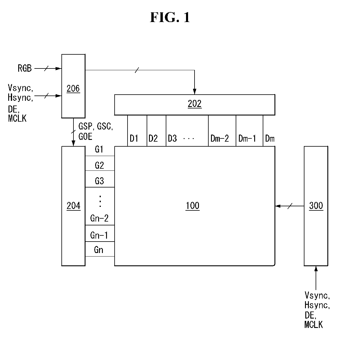
- the display device includes a display panel 100, a display driving circuit, a sensor driving circuit 300, and the like.
- a pixel array of the display panel 100 includes pixels PIX formed in pixel areas defined by data lines D1 to Dm (where m is a positive integer) and gate lines G1 to Gn (where n is a positive integer).
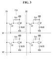
- the pixels PIX may be implemented as pixels of the LCD shown in FIG. 2 or pixels of the OLED display shown in FIG. 3 .
- the pixel PIX of the LCD includes thin film transistors (TFTs) formed at crossings of the data lines D1 to Dm and the gate lines G1 to Gn, a pixel electrode charged to a data voltage, a common electrode to which a common voltage Vcom is supplied, a storage capacitor Cst which is connected to the pixel electrode and holds a voltage of a liquid crystal cell, and the like.
- TFTs thin film transistors
- the pixel PIX of the OLED display includes a switching TFT ST, a driving TFT DT connected to the switching TFT ST, an OLED and a storage capacitor Cst which are connected to the driving TFT DT, electrodes to which a high potential pixel power voltage VDD and a low potential pixel power voltage VSS are supplied, and the like.
- Each pixel PIX may further include a compensation circuit which senses and compensates a threshold voltage and mobility of the driving TFT DT.
- the display panel 100 may further include color filters and black matrixes.
- a backlight unit may be disposed under a back surface of the display panel 100.
- the pixels PIX of the display panel 100 are driven by the display driving circuit.
- the display driving circuit applies data of an input image to the pixels PIX for a vertical active time AT.
- the display driving circuit includes a data driving circuit 202, a gate driving circuit (or a scan driving circuit) 204, and a timing controller 206.
- Digital video data RGB of an input image is input to the timing controller 206 in synchronization with timing signals Vsync, Hsync, DE, and MCLK for the vertical active time AT.
- the data driving circuit 202 converts the digital video data RGB received from the timing controller 206 into gamma compensation voltages and outputs the data voltage for the vertical active time AT.
- the data voltage output from the data driving circuit 202 is supplied to the pixels PIX through the data lines D1 to Dm for the vertical active time AT. Data of a new input image is not input to the data driving circuit 202 for a vertical blank time VB.
- the gate driving circuit 204 is driven for the vertical active time AT. More specifically, the gate driving circuit 204 sequentially supplies a gate pulse (or a scan pulse) synchronized with the data voltage to the gate lines G1 to Gn and selects lines of the display panel 100, to which the data voltage is applied. The gate pulse swings between a gate high voltage VGH and a gate low voltage VGL. The gate driving circuit 204 does not generate the gate pulse for the vertical blank time VB. Thus, the data driving circuit 202 and the gate driving circuit 204 do not generate a new output for the vertical blank time VB under the control of the timing controller 206.
- the timing controller 206 transmits the digital video data RGB of the input image received from a host system (not shown) to the data driving circuit 202 in synchronization with the timing signals Vsync, Hsync, DE, and MCLK.
- the digital video data RGB of the input image is synchronized with a data enable signal DE and is input to the timing controller 206 for the vertical active time AT.
- the digital video data RGB of the input image and the data enable signal DE are not input to the timing controller 206 for the vertical blank time VB.
- the host system may be implemented as one of a television system, a set-top box, a navigation system, a DVD player, a Blu-ray player, a personal computer (PC), a home theater system, and a phone system.
- the host system includes a system on chip (SoC) including a scaler embedded therein and thus converts the digital video data of the input image into a format suitable for displaying on the display panel 100.
- SoC system on chip
- the host system transmits the digital video data and the timing signals Vsync, Hsync, DE, and MCLK to the timing controller 206.
- the host system runs an application associated with coordinate information XY of a touch input or a gesture input received from the sensor driving circuit 300.
- the timing signals Vsync, Hsync, DE, and MCLK input to the timing controller 206 include a vertical sync signal Vsync, a horizontal sync signal Hsync, a data enable signal DE, and a main clock MCLK.
- the timing controller 206 generates timing control signals for controlling operation timings of the data driving circuit 202 and the scan driving circuit 204 using the timing signals Vsync, Hsync, DE, and MCLK.
- the timing controller 206 does not reduce the vertical active time AT, in which new data is applied to the pixels, and controls the vertical active time AT as much as the general display devices. In other words, the timing controller 206 does not secure a touch sensing period or a gesture sensing period by modulating the timing signals Vsync, Hsync, DE, and MCLK and reducing the vertical active time AT. Thus, the display device according to the embodiment of the invention does not reduce a data charge time of the pixels so as to secure the touch sensing period or the gesture sensing period.
- the sensor driving circuit 300 applies a gesture sensing driving signal SP to the common voltage of the display panel 100 for the vertical blank time VB, in which there is no data of the input image, and analyzes a change amount of the gesture sensing driving signal SP, thereby deciding a gesture input.
- the gesture input is position input of an object, which does not contact the screen of the display panel 100 and is positioned at the front of the screen of the display panel 100.
- a touch input is position input of an object contacting the screen of the display panel 100.
- the display device according to the embodiment of the invention does not sense the touch input and senses the gesture input for the vertical blank time VB.
- the sensor driving circuit 300 analyzes the gesture sensing driving signal SP using a predetermined gesture recognition algorithm. More specifically, the sensor driving circuit 300 decides that the gesture input is generated when the change amount of the gesture sensing driving signal SP is equal to or greater than a predetermined threshold value.
- the gesture recognition algorithm may use a known algorithm.
- the common electrode means an electrode commonly connected to all of the pixels inside the screen (i.e., a display area shown in FIG. 4 ) of the display panel.
- the common electrode may be the common electrode, to which the common voltage Vcom is supplied, in the LCD shown in FIG. 2 , or the common electrode, to which the high potential pixel power voltage VDD and the low potential pixel power voltage VSS are supplied, in the OLED display shown in FIG. 3 .
- the common voltages Vcom, VDD, and VSS of the pixels are supplied to the common electrode for the vertical active time AT.
- the gesture sensing driving signal SP is input to the common electrode for the vertical blank time VB.
- the sensor driving circuit 300 does not decide a direction or a distance of the gesture input for the vertical blank time VB and may decide only whether or not there is the gesture input. In this instance, because the host system may decide whether or not there is the gesture input, it may be used in a simple conversion function, for example, power-on or power-off.
- a voltage of the gesture sensing driving signal SP may be properly set in consideration of a height capable of sensing or an intensity of an electric field.
- the gesture sensing driving signal SP is generated at a voltage greater than the common voltage Vcom as shown in FIGS. 2 and 4 .
- the gesture sensing driving signal SP may be generated at the same voltage as a touch sensing driving signal applied to a capacitive sensor, which was used in an existing touch screen, or may be generated at a voltage greater than the touch sensing driving signal. Further, the gesture sensing driving signal SP may be generated as a signal of a multistep waveform, in which an initial voltage is set to a high value.
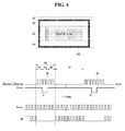
- FIG. 4 shows gesture sensing timing according to the embodiment of the invention in display timing of video electronics standards association (VESA) standard.
- VESA video electronics standards association
- the data enable signal DE is synchronized with data of the input image.
- a period of one pulse of the data enable signal DE is one horizontal period, and a high logic period of the data enable signal DE indicates data input timing on one line.
- One horizontal period is a horizontal address time required to apply data to pixels on one line of the display panel 100.
- the data enable signal DE and the data of the input image are input for the vertical active time AT and are not input for the vertical blank time VB.
- the vertical active time AT is a vertical address time required to display data corresponding to an amount of one frame on all of the pixels of the display area of the display panel 100, on which an image is displayed.
- One frame period is a time required to display the data of one frame on the display panel 100 and is equal to a sum of one vertical active time AT and one vertical blank time VB.
- the vertical blank time VB includes a vertical sync time VS, a vertical front porch FP, and a vertical back porch BP.
- the vertical sync time VS is a time ranging from a falling edge to a rising edge of the vertical sync signal Vsync and indicates start timing (or end timing) of one screen.
- the vertical blank time VB is equal to or greater than about 475 ⁇ s in full high definition (FHD) resolution. For the vertical blank time VB, several tens to several hundreds of gesture sensing operations may be performed.
- FHD full high definition
- the vertical front porch FP is a time ranging from a falling edge of the last data enable signal DE indicating data timing of the last line in the data of one frame to a start time point of the vertical blank time VB.
- the vertical back porch BP is a time ranging from an end time point of the vertical blank time VB to a rising edge of a first data enable signal DE indicating data timing of a first line in the data of one frame.
- the display driving circuit applies the data of the input image to the pixels for the vertical active time AT.
- the sensor driving circuit 300 applies the gesture sensing driving signal SP to the common electrode of the display panel 100 for the vertical blank time VB and senses the gesture input.
- FIG. 5 is a block diagram showing in detail the sensor driving circuit 300.
- the sensor driving circuit 300 includes a multiplexer 302, a gesture sensing driver 304, and an algorithm execution unit 306.
- the multiplexer 302 supplies the common voltages Vcom, VDD, and VSS to the common electrode of the display panel 100 for the vertical active time AT and supplies the gesture sensing driving signal SP to the common electrode of the display panel 100 for the vertical blank time VB.
- the gesture sensing driver 304 generates the gesture sensing driving signal SP for the vertical blank time VB and supplies the gesture sensing driving signal SP to the multiplexer 302.
- the gesture sensing driver 304 converts a change amount of the gesture sensing driving signal SP received through the multiplexer 302 into digital data using an analog-to-digital converter (ADC) and transmits the digital data to the algorithm execution unit 306.
- ADC analog-to-digital converter
- the algorithm execution unit 306 compares the digital data received from the gesture sensing driver 304 with a predetermined threshold value. The algorithm execution unit 306 decides that the gesture input is generated when the change amount of the gesture sensing driving signal SP is equal to or greater than the predetermined threshold value, and generates an interrupt signal. If the common electrode is divided into a plurality of common electrodes and a direction and space coordinates of the gesture input are sensed, the algorithm execution unit 306 may transmit space coordinates of a gesture input position to the host system, when the gesture input is sensed.
- the algorithm execution unit 306 may be implemented as a microcontroller unit (MCU) and a memory.
- MCU microcontroller unit
- the common electrode of the display panel 100 may be divided as shown in FIGS. 6 to 8 , so that the recognition of various operations is possible.
- FIG. 6 is an equivalent circuit diagram showing an example of dividing the common electrode of the display panel to implement a mutual capacitive sensor matrix.
- FIG. 7 is an enlarged plane view of a portion of the mutual capacitive sensor matrix.
- the mutual capacitive sensor matrix includes Tx lines Tx1 to TxN and Rx lines Rx1 to RxM which are perpendicular to the Tx lines Tx1 to TxN with a dielectric layer interposed therebetween.
- the common electrode of the display panel may be divided into the Tx lines Tx1 to TxN or may be divided into the Tx lines Tx1 to TxN and the Rx lines Rx1 to RxM.
- the common electrode supplies the common voltages Vcom, VDD, and VSS to the pixels for the vertical active time AT and is used as the plurality of sensor electrodes for the vertical blank time VB.
- the Tx lines Tx1 to TxN and the Rx lines Rx1 to RxM have the size larger than the pixel PIX and are connected to the plurality of pixels.
- a mutual capacitance Cm is formed at each crossing of the Tx lines Tx1 to TxN and the Rx lines Rx1 to RxM.
- the sensor driving circuit 300 applies the gesture sensing driving signal SP to the Tx lines Tx1 to TxN divided from the common electrode and receives the gesture sensing driving signal SP through the Rx lines Rx1 to RxM.
- the Rx lines Rx1 to RxM are implemented by the divided common electrodes or are implemented by the data lines D1 to Dm or the gate lines G1 to Gn connected to the pixels. Because the pixels hold previous data for the vertical blank time VB, the data lines D1 to Dm or the gate lines G1 to Gn may be used as the Rx lines Rx1 to RxM for the vertical blank time VB.
- the display device does not additionally form the Tx lines Tx1 to TxN and the Rx lines Rx1 to RxM when the mutual capacitive sensor is used for the gesture sensing, and may implement the Tx lines Tx1 to TxN and the Rx lines Rx1 to RxM using components of an existing pixel array.
- FIG. 8 is an equivalent circuit diagram showing an example of dividing the common electrode of the display panel to implement a self capacitive sensor matrix.
- the self capacitive sensor matrix includes sensor electrodes TE1 to TEi arranged in a matrix form and sensor lines respectively connected to the sensor electrodes TE1 to TEi.
- the common electrode of the display panel may be divided into the sensor electrodes TE1 to TEi and the sensor lines.
- the common electrode supplies the common voltages Vcom, VDD, and VSS to the pixels for the vertical active time AT and is used as the plurality of sensor electrodes for the vertical blank time VB.
- the sensor driving circuit 300 applies the gesture sensing driving signal SP to the sensor electrodes TE1 to TEi divided from the common electrode and receives the gesture sensing driving signal SP through the sensor lines.
- the embodiment of the invention does not affect the display drive.
- the embodiment of the invention does not add a separate sensor for the gesture sensing to the display panel and senses the gesture for the vertical blank time using the common electrode commonly connected to the pixels.
Landscapes
- Engineering & Computer Science (AREA)
- Theoretical Computer Science (AREA)
- Physics & Mathematics (AREA)
- General Physics & Mathematics (AREA)
- General Engineering & Computer Science (AREA)
- Computer Hardware Design (AREA)
- Human Computer Interaction (AREA)
- Multimedia (AREA)
- Crystallography & Structural Chemistry (AREA)
- Chemical & Material Sciences (AREA)
- Control Of Indicators Other Than Cathode Ray Tubes (AREA)
- Liquid Crystal Display Device Control (AREA)
- Control Of El Displays (AREA)
Abstract

Description
- Embodiments of the invention relate to a display device and a method for driving the same.
- User interface (UI) is configured so that users are able to communicate with various electronic devices and thus can easily and comfortably control the electronic devices as they desire. Examples of the user interface include a keypad, a keyboard, a mouse, an on-screen display (OSD), and a remote controller having an infrared communication function or a radio frequency (RF) communication function. User interface technology has continuously expanded to increase user's sensibility and handling convenience. The user interface has been developed to include touch UI, voice recognition UI, 3D UI, etc. A gesture UI for sensing user's gestures has been recently applied to household appliances.
- The gesture UI senses the user's gestures or object's movement on a space using a camera or a motion sensor. A separate sensor for the gesture sensing has to be added so as to implement the gesture UI in a display device. However, the separate sensor results in an increase in the cost of the display device.
- In one aspect, there is a display device comprising a display panel including a common electrode commonly connected to pixels, a display driving circuit configured to apply a data voltage to the pixels for the vertical active time, and a sensor driving circuit configured to apply a gesture sensing driving signal to the common electrode for the vertical blank time and sense a gesture input.
- In another aspect, there is a method for driving a display device including a common electrode commonly connected to pixels, comprising applying a data voltage to the pixels for the vertical active time, and applying a gesture sensing driving signal to the common electrode for the vertical blank time and sensing a gesture input.
- The accompanying drawings, which are included to provide a further understanding of the invention and are incorporated in and constitute a part of this specification, illustrate embodiments of the invention and together with the description serve to explain the principles of the invention. In the drawings:
-
FIG. 1 is a block diagram of a display device according to an exemplary embodiment of the invention; -
FIG. 2 is an equivalent circuit diagram showing pixels of a liquid crystal display (LCD); -
FIG. 3 is an equivalent circuit showing pixels of an organic light emitting diode (OLED) display; -
FIG. 4 shows gesture sensing timing according to an exemplary embodiment of the invention in display timing of video electronics standards association (VESA) standard; -
FIG. 5 is a block diagram showing in detail a sensor driving circuit shown inFIG. 1 ; -
FIG. 6 is an equivalent circuit diagram showing an example of dividing a common electrode of a display panel to implement a mutual capacitive sensor matrix; -
FIG. 7 is an enlarged plane view of a portion of a mutual capacitive sensor matrix; and -
FIG. 8 is an equivalent circuit diagram showing an example of dividing a common electrode of a display panel to implement a self capacitive sensor matrix. - A display device according to an exemplary embodiment of the invention may be implemented as a flat panel display, such as a liquid crystal display (LCD) and an organic light emitting diode (OLED) display.
- The display device according to the embodiment of the invention implements a gesture sensor using components for driving pixels of a display panel and does not add a separate the gesture sensor. The display device according to the embodiment of the invention senses gestures in a blank period, in which image data is not input, so as not to reduce a length of a display driving period and not to affect a display drive.
- A gesture sensor according to the embodiment of the invention may be implemented as a capacitive sensor. The capacitive sensor may be implemented as a self capacitive sensor or a mutual capacitive sensor. The self capacitive sensors are respectively connected to sensor lines along one direction. The mutual capacitive sensor is formed at a crossing of two sensor lines, which are perpendicular to each other with a dielectric layer interposed therebetween.
- Reference will now be made in detail to embodiments of the invention, examples of which are illustrated in the accompanying drawings. Wherever possible, the same reference numbers will be used throughout the drawings to refer to the same or like parts. It will be paid attention that detailed description of known arts will be omitted if it is determined that the arts can mislead the embodiments of the invention.
- As shown in
FIGS. 1 to 4 , the display device according to the embodiment of the invention includes adisplay panel 100, a display driving circuit, asensor driving circuit 300, and the like. - A pixel array of the
display panel 100 includes pixels PIX formed in pixel areas defined by data lines D1 to Dm (where m is a positive integer) and gate lines G1 to Gn (where n is a positive integer). The pixels PIX may be implemented as pixels of the LCD shown inFIG. 2 or pixels of the OLED display shown inFIG. 3 . - As shown in
FIG. 2 , the pixel PIX of the LCD includes thin film transistors (TFTs) formed at crossings of the data lines D1 to Dm and the gate lines G1 to Gn, a pixel electrode charged to a data voltage, a common electrode to which a common voltage Vcom is supplied, a storage capacitor Cst which is connected to the pixel electrode and holds a voltage of a liquid crystal cell, and the like. - As shown in
FIG. 3 , the pixel PIX of the OLED display includes a switching TFT ST, a driving TFT DT connected to the switching TFT ST, an OLED and a storage capacitor Cst which are connected to the driving TFT DT, electrodes to which a high potential pixel power voltage VDD and a low potential pixel power voltage VSS are supplied, and the like. Each pixel PIX may further include a compensation circuit which senses and compensates a threshold voltage and mobility of the driving TFT DT. - The
display panel 100 may further include color filters and black matrixes. When the LCD is implemented as the display device, a backlight unit may be disposed under a back surface of thedisplay panel 100. - The pixels PIX of the
display panel 100 are driven by the display driving circuit. The display driving circuit applies data of an input image to the pixels PIX for a vertical active time AT. The display driving circuit includes adata driving circuit 202, a gate driving circuit (or a scan driving circuit) 204, and atiming controller 206. - Digital video data RGB of an input image is input to the
timing controller 206 in synchronization with timing signals Vsync, Hsync, DE, and MCLK for the vertical active time AT. Thedata driving circuit 202 converts the digital video data RGB received from thetiming controller 206 into gamma compensation voltages and outputs the data voltage for the vertical active time AT. The data voltage output from thedata driving circuit 202 is supplied to the pixels PIX through the data lines D1 to Dm for the vertical active time AT. Data of a new input image is not input to thedata driving circuit 202 for a vertical blank time VB. - The
gate driving circuit 204 is driven for the vertical active time AT. More specifically, thegate driving circuit 204 sequentially supplies a gate pulse (or a scan pulse) synchronized with the data voltage to the gate lines G1 to Gn and selects lines of thedisplay panel 100, to which the data voltage is applied. The gate pulse swings between a gate high voltage VGH and a gate low voltage VGL. Thegate driving circuit 204 does not generate the gate pulse for the vertical blank time VB. Thus, thedata driving circuit 202 and thegate driving circuit 204 do not generate a new output for the vertical blank time VB under the control of thetiming controller 206. - The
timing controller 206 transmits the digital video data RGB of the input image received from a host system (not shown) to thedata driving circuit 202 in synchronization with the timing signals Vsync, Hsync, DE, and MCLK. The digital video data RGB of the input image is synchronized with a data enable signal DE and is input to thetiming controller 206 for the vertical active time AT. On the other hand, the digital video data RGB of the input image and the data enable signal DE are not input to thetiming controller 206 for the vertical blank time VB. - The host system may be implemented as one of a television system, a set-top box, a navigation system, a DVD player, a Blu-ray player, a personal computer (PC), a home theater system, and a phone system. The host system includes a system on chip (SoC) including a scaler embedded therein and thus converts the digital video data of the input image into a format suitable for displaying on the
display panel 100. The host system transmits the digital video data and the timing signals Vsync, Hsync, DE, and MCLK to thetiming controller 206. The host system runs an application associated with coordinate information XY of a touch input or a gesture input received from thesensor driving circuit 300. - The timing signals Vsync, Hsync, DE, and MCLK input to the
timing controller 206 include a vertical sync signal Vsync, a horizontal sync signal Hsync, a data enable signal DE, and a main clock MCLK. Thetiming controller 206 generates timing control signals for controlling operation timings of thedata driving circuit 202 and thescan driving circuit 204 using the timing signals Vsync, Hsync, DE, and MCLK. - The
timing controller 206 does not reduce the vertical active time AT, in which new data is applied to the pixels, and controls the vertical active time AT as much as the general display devices. In other words, thetiming controller 206 does not secure a touch sensing period or a gesture sensing period by modulating the timing signals Vsync, Hsync, DE, and MCLK and reducing the vertical active time AT. Thus, the display device according to the embodiment of the invention does not reduce a data charge time of the pixels so as to secure the touch sensing period or the gesture sensing period. - The
sensor driving circuit 300 applies a gesture sensing driving signal SP to the common voltage of thedisplay panel 100 for the vertical blank time VB, in which there is no data of the input image, and analyzes a change amount of the gesture sensing driving signal SP, thereby deciding a gesture input. The gesture input is position input of an object, which does not contact the screen of thedisplay panel 100 and is positioned at the front of the screen of thedisplay panel 100. On the other hand, a touch input is position input of an object contacting the screen of thedisplay panel 100. The display device according to the embodiment of the invention does not sense the touch input and senses the gesture input for the vertical blank time VB. - The
sensor driving circuit 300 analyzes the gesture sensing driving signal SP using a predetermined gesture recognition algorithm. More specifically, thesensor driving circuit 300 decides that the gesture input is generated when the change amount of the gesture sensing driving signal SP is equal to or greater than a predetermined threshold value. The gesture recognition algorithm may use a known algorithm. - The common electrode means an electrode commonly connected to all of the pixels inside the screen (i.e., a display area shown in
FIG. 4 ) of the display panel. For example, the common electrode may be the common electrode, to which the common voltage Vcom is supplied, in the LCD shown inFIG. 2 , or the common electrode, to which the high potential pixel power voltage VDD and the low potential pixel power voltage VSS are supplied, in the OLED display shown inFIG. 3 . Namely, the common voltages Vcom, VDD, and VSS of the pixels are supplied to the common electrode for the vertical active time AT. On the other hand, the gesture sensing driving signal SP is input to the common electrode for the vertical blank time VB. - If the common electrode is not divided inside the display panel and is connected to all of the pixels inside the screen (i.e., the display area shown in
FIG. 4 ) of the display panel, thesensor driving circuit 300 does not decide a direction or a distance of the gesture input for the vertical blank time VB and may decide only whether or not there is the gesture input. In this instance, because the host system may decide whether or not there is the gesture input, it may be used in a simple conversion function, for example, power-on or power-off. - A voltage of the gesture sensing driving signal SP may be properly set in consideration of a height capable of sensing or an intensity of an electric field. In the LCD, the gesture sensing driving signal SP is generated at a voltage greater than the common voltage Vcom as shown in
FIGS. 2 and4 . The gesture sensing driving signal SP may be generated at the same voltage as a touch sensing driving signal applied to a capacitive sensor, which was used in an existing touch screen, or may be generated at a voltage greater than the touch sensing driving signal. Further, the gesture sensing driving signal SP may be generated as a signal of a multistep waveform, in which an initial voltage is set to a high value. -
FIG. 4 shows gesture sensing timing according to the embodiment of the invention in display timing of video electronics standards association (VESA) standard. - As shown in
FIG. 4 , the data enable signal DE is synchronized with data of the input image. A period of one pulse of the data enable signal DE is one horizontal period, and a high logic period of the data enable signal DE indicates data input timing on one line. One horizontal period is a horizontal address time required to apply data to pixels on one line of thedisplay panel 100. - The data enable signal DE and the data of the input image are input for the vertical active time AT and are not input for the vertical blank time VB. The vertical active time AT is a vertical address time required to display data corresponding to an amount of one frame on all of the pixels of the display area of the
display panel 100, on which an image is displayed. One frame period is a time required to display the data of one frame on thedisplay panel 100 and is equal to a sum of one vertical active time AT and one vertical blank time VB. - The vertical blank time VB includes a vertical sync time VS, a vertical front porch FP, and a vertical back porch BP. The vertical sync time VS is a time ranging from a falling edge to a rising edge of the vertical sync signal Vsync and indicates start timing (or end timing) of one screen.
- The vertical blank time VB is equal to or greater than about 475 µs in full high definition (FHD) resolution. For the vertical blank time VB, several tens to several hundreds of gesture sensing operations may be performed.
- The vertical front porch FP is a time ranging from a falling edge of the last data enable signal DE indicating data timing of the last line in the data of one frame to a start time point of the vertical blank time VB. The vertical back porch BP is a time ranging from an end time point of the vertical blank time VB to a rising edge of a first data enable signal DE indicating data timing of a first line in the data of one frame.
- The display driving circuit applies the data of the input image to the pixels for the vertical active time AT. The
sensor driving circuit 300 applies the gesture sensing driving signal SP to the common electrode of thedisplay panel 100 for the vertical blank time VB and senses the gesture input. -
FIG. 5 is a block diagram showing in detail thesensor driving circuit 300. - As shown in
FIG. 5 , thesensor driving circuit 300 includes amultiplexer 302, agesture sensing driver 304, and analgorithm execution unit 306. - The
multiplexer 302 supplies the common voltages Vcom, VDD, and VSS to the common electrode of thedisplay panel 100 for the vertical active time AT and supplies the gesture sensing driving signal SP to the common electrode of thedisplay panel 100 for the vertical blank time VB. - The
gesture sensing driver 304 generates the gesture sensing driving signal SP for the vertical blank time VB and supplies the gesture sensing driving signal SP to themultiplexer 302. Thegesture sensing driver 304 converts a change amount of the gesture sensing driving signal SP received through themultiplexer 302 into digital data using an analog-to-digital converter (ADC) and transmits the digital data to thealgorithm execution unit 306. - The
algorithm execution unit 306 compares the digital data received from thegesture sensing driver 304 with a predetermined threshold value. Thealgorithm execution unit 306 decides that the gesture input is generated when the change amount of the gesture sensing driving signal SP is equal to or greater than the predetermined threshold value, and generates an interrupt signal. If the common electrode is divided into a plurality of common electrodes and a direction and space coordinates of the gesture input are sensed, thealgorithm execution unit 306 may transmit space coordinates of a gesture input position to the host system, when the gesture input is sensed. Thealgorithm execution unit 306 may be implemented as a microcontroller unit (MCU) and a memory. - The common electrode of the
display panel 100 may be divided as shown inFIGS. 6 to 8 , so that the recognition of various operations is possible. -
FIG. 6 is an equivalent circuit diagram showing an example of dividing the common electrode of the display panel to implement a mutual capacitive sensor matrix.FIG. 7 is an enlarged plane view of a portion of the mutual capacitive sensor matrix. - As shown in
FIGS. 6 and7 , the mutual capacitive sensor matrix includes Tx lines Tx1 to TxN and Rx lines Rx1 to RxM which are perpendicular to the Tx lines Tx1 to TxN with a dielectric layer interposed therebetween. - The common electrode of the display panel may be divided into the Tx lines Tx1 to TxN or may be divided into the Tx lines Tx1 to TxN and the Rx lines Rx1 to RxM. Thus, the common electrode supplies the common voltages Vcom, VDD, and VSS to the pixels for the vertical active time AT and is used as the plurality of sensor electrodes for the vertical blank time VB.
- The Tx lines Tx1 to TxN and the Rx lines Rx1 to RxM have the size larger than the pixel PIX and are connected to the plurality of pixels. A mutual capacitance Cm is formed at each crossing of the Tx lines Tx1 to TxN and the Rx lines Rx1 to RxM.
- For the vertical blank time VB, the
sensor driving circuit 300 applies the gesture sensing driving signal SP to the Tx lines Tx1 to TxN divided from the common electrode and receives the gesture sensing driving signal SP through the Rx lines Rx1 to RxM. The Rx lines Rx1 to RxM are implemented by the divided common electrodes or are implemented by the data lines D1 to Dm or the gate lines G1 to Gn connected to the pixels. Because the pixels hold previous data for the vertical blank time VB, the data lines D1 to Dm or the gate lines G1 to Gn may be used as the Rx lines Rx1 to RxM for the vertical blank time VB. Thus, the display device according to the embodiment of the invention does not additionally form the Tx lines Tx1 to TxN and the Rx lines Rx1 to RxM when the mutual capacitive sensor is used for the gesture sensing, and may implement the Tx lines Tx1 to TxN and the Rx lines Rx1 to RxM using components of an existing pixel array. -
FIG. 8 is an equivalent circuit diagram showing an example of dividing the common electrode of the display panel to implement a self capacitive sensor matrix. - As shown in
FIG. 8 , the self capacitive sensor matrix includes sensor electrodes TE1 to TEi arranged in a matrix form and sensor lines respectively connected to the sensor electrodes TE1 to TEi. - The common electrode of the display panel may be divided into the sensor electrodes TE1 to TEi and the sensor lines. Thus, the common electrode supplies the common voltages Vcom, VDD, and VSS to the pixels for the vertical active time AT and is used as the plurality of sensor electrodes for the vertical blank time VB.
- For the vertical blank time VB, the
sensor driving circuit 300 applies the gesture sensing driving signal SP to the sensor electrodes TE1 to TEi divided from the common electrode and receives the gesture sensing driving signal SP through the sensor lines. - As described above, because the embodiment of the invention does not reduce the vertical active time in one frame period of the display device, the embodiment of the invention does not affect the display drive. The embodiment of the invention does not add a separate sensor for the gesture sensing to the display panel and senses the gesture for the vertical blank time using the common electrode commonly connected to the pixels.
- Although embodiments have been described with reference to a number of illustrative embodiments thereof, it should be understood that numerous other modifications and embodiments can be devised by those skilled in the art that will fall within the scope of the principles of this disclosure. More particularly, various variations and modifications are possible in the component parts and/or arrangements of the subject combination arrangement within the scope of the disclosure, the drawings and the appended claims. In addition to variations and modifications in the component parts and/or arrangements, alternative uses will also be apparent to those skilled in the art.
Claims (10)
- A display device, in which one frame period is divided into a vertical active time, in which data of an input image is input, and a vertical blank time, in which the data of the input image is not input, comprising:a display panel including a common electrode commonly connected to pixels;a display driving circuit configured to apply a data voltage to the pixels for the vertical active time; anda sensor driving circuit configured to apply a gesture sensing driving signal to the common electrode for the vertical blank time and sense a gesture input.
- The display device of claim 1, wherein the common electrode is not divided inside the display panel.
- The display device of claim 2, wherein the sensor driving circuit decides only whether or not there is the gesture input for the vertical blank time.
- The display device of claim 1, wherein the common electrode is divided into a plurality of common electrodes.
- The display device of claim 1, wherein the sensor driving circuit decides the gesture input for the vertical blank time and outputs coordinates of a gesture input position.
- The display device of claim 4, wherein the divided common electrode operates as a mutual capacitive sensor matrix for the vertical blank time.
- The display device of claim 4, wherein the divided common electrode operates as a self capacitive sensor matrix for the vertical blank time.
- A method for driving a display device including a common electrode commonly connected to pixels, in which one frame period is divided into a vertical active time, in which data of an input image is input, and a vertical blank time, in which the data of the input image is not input, the method comprising:applying a data voltage to the pixels for the vertical active time; andapplying a gesture sensing driving signal to the common electrode for the vertical blank time and sensing a gesture input.
- The method of claim 8, wherein the applying of the gesture sensing driving signal to the common electrode for the vertical blank time and the sensing of the gesture input includes deciding only whether or not there is the gesture input for the vertical blank time,
wherein the common electrode is not divided inside the display panel. - The method of claim 9, wherein the applying of the gesture sensing driving signal to the common electrode for the vertical blank time and the sensing of the gesture input includes:deciding the gesture input for the vertical blank time and generating coordinates of a gesture input position; anddividing the common electrode into a plurality of common electrodes.
Applications Claiming Priority (1)
| Application Number | Priority Date | Filing Date | Title |
|---|---|---|---|
| KR1020130140535A KR102063349B1 (en) | 2013-11-19 | 2013-11-19 | Display device and driving method thereof |
Publications (2)
| Publication Number | Publication Date |
|---|---|
| EP2874145A1 true EP2874145A1 (en) | 2015-05-20 |
| EP2874145B1 EP2874145B1 (en) | 2018-01-10 |
Family
ID=51167661
Family Applications (1)
| Application Number | Title | Priority Date | Filing Date |
|---|---|---|---|
| EP14175545.4A Active EP2874145B1 (en) | 2013-11-19 | 2014-07-03 | Display device and method for driving the same |
Country Status (6)
| Country | Link |
|---|---|
| US (1) | US10002590B2 (en) |
| EP (1) | EP2874145B1 (en) |
| JP (1) | JP6084186B2 (en) |
| KR (1) | KR102063349B1 (en) |
| CN (1) | CN104657068B (en) |
| TW (1) | TWI543055B (en) |
Cited By (1)
| Publication number | Priority date | Publication date | Assignee | Title |
|---|---|---|---|---|
| EP3159778A1 (en) * | 2015-10-20 | 2017-04-26 | LG Display Co., Ltd. | Display device having touch sensor and driving method thereof |
Families Citing this family (12)
| Publication number | Priority date | Publication date | Assignee | Title |
|---|---|---|---|---|
| EP3137981A4 (en) * | 2014-04-30 | 2017-12-06 | Hewlett-Packard Development Company, L.P. | Multi architecture manager |
| KR20160087481A (en) * | 2015-01-13 | 2016-07-22 | 삼성디스플레이 주식회사 | Touch Screen Panel and Driving Method Thereof |
| US9939972B2 (en) | 2015-04-06 | 2018-04-10 | Synaptics Incorporated | Matrix sensor with via routing |
| US9671915B2 (en) | 2015-06-30 | 2017-06-06 | Synaptics Incorporated | Avoidance of bending effects in a touch sensor device |
| US9971463B2 (en) | 2015-09-29 | 2018-05-15 | Synaptics Incorporated | Row-based sensing on matrix pad sensors |
| KR102446751B1 (en) * | 2015-12-01 | 2022-09-26 | 엘지디스플레이 주식회사 | Display device and its driving circuit and driving method |
| CN106297713B (en) * | 2016-09-26 | 2020-01-24 | 苏州佳世达电通有限公司 | Display method and display device for improving image dynamic blurring |
| KR102215481B1 (en) * | 2016-12-15 | 2021-02-15 | 주식회사 지2터치 | Display device having touch screen |
| TWI625660B (en) * | 2017-01-09 | 2018-06-01 | 義隆電子股份有限公司 | Touch display system and operation method for touch display system |
| TWI629634B (en) * | 2017-08-17 | 2018-07-11 | 義隆電子股份有限公司 | Method for performing touch sensing on touch display device and touch display device |
| TWI699602B (en) * | 2019-01-21 | 2020-07-21 | 友達光電股份有限公司 | Display device |
| US11508273B2 (en) * | 2020-11-12 | 2022-11-22 | Synaptics Incorporated | Built-in test of a display driver |
Citations (4)
| Publication number | Priority date | Publication date | Assignee | Title |
|---|---|---|---|---|
| US20130222279A1 (en) * | 2012-02-23 | 2013-08-29 | Chunghwa Picture Tubes, Ltd. | Touch display apparatus |
| US20130249853A1 (en) * | 2012-03-23 | 2013-09-26 | Japan Display West, Inc. | Detection device, detection method, program and display apparatus |
| US20130265256A1 (en) * | 2012-04-07 | 2013-10-10 | Cambridge Touch Technologies, Ltd. | Pressure sensing display device |
| US20130285952A1 (en) * | 2012-04-27 | 2013-10-31 | Orise Technology Co., Ltd. | In-cell multi-touch display panel system |
Family Cites Families (23)
| Publication number | Priority date | Publication date | Assignee | Title |
|---|---|---|---|---|
| JP2003066417A (en) | 2001-08-22 | 2003-03-05 | Sharp Corp | Touch sensor integrated display |
| KR101209042B1 (en) * | 2005-11-30 | 2012-12-06 | 삼성디스플레이 주식회사 | Display device and testing method thereof |
| JP5570679B2 (en) * | 2006-12-27 | 2014-08-13 | エルジー ディスプレイ カンパニー リミテッド | Touch panel device |
| KR101359921B1 (en) * | 2007-03-02 | 2014-02-07 | 삼성디스플레이 주식회사 | Display device |
| WO2009067224A1 (en) * | 2007-11-19 | 2009-05-28 | Cirque Corporation | Touchpad combined with a display and having proximity and touch sensing capabilities |
| JP4816668B2 (en) | 2008-03-28 | 2011-11-16 | ソニー株式会社 | Display device with touch sensor |
| JP5178633B2 (en) | 2009-05-29 | 2013-04-10 | 株式会社ジャパンディスプレイウェスト | Touch sensor, display device, and electronic device |
| KR101255283B1 (en) * | 2009-09-29 | 2013-04-15 | 엘지디스플레이 주식회사 | Liquid Crystal Display Device |
| TW201115557A (en) * | 2009-10-16 | 2011-05-01 | Aussmak Optoelectronic Corp | Driving method of touch display module |
| KR101790977B1 (en) * | 2010-10-08 | 2017-10-26 | 엘지디스플레이 주식회사 | Liquid crystal display device |
| KR101457743B1 (en) * | 2011-02-25 | 2014-11-04 | 엘지디스플레이 주식회사 | Touch sensor integrated display device |
| KR101819676B1 (en) * | 2011-02-25 | 2018-03-02 | 엘지디스플레이 주식회사 | Touch sensor integrated liquid cryctal display device |
| US20120306926A1 (en) * | 2011-06-06 | 2012-12-06 | Apple Inc. | Inline scaling unit for mirror mode |
| KR101879479B1 (en) * | 2011-09-07 | 2018-07-17 | 시냅틱스 인코포레이티드 | Capacitive sensing during non-display update times |
| KR101909985B1 (en) * | 2011-12-03 | 2018-10-22 | 엘지디스플레이 주식회사 | Liquid crystal display apparatus and method for driving the same |
| KR101537435B1 (en) * | 2011-12-13 | 2015-07-16 | 엘지디스플레이 주식회사 | Touch sensor integrated type display and driving method thereof |
| US9342181B2 (en) * | 2012-01-09 | 2016-05-17 | Nvidia Corporation | Touch-screen input/output device touch sensing techniques |
| AU2013205613B2 (en) * | 2012-05-04 | 2017-12-21 | Samsung Electronics Co., Ltd. | Terminal and method for controlling the same based on spatial interaction |
| KR20130136671A (en) * | 2012-06-05 | 2013-12-13 | 삼성디스플레이 주식회사 | Capacitive touch panel sensor and touch panel display device having the same |
| US10095358B2 (en) * | 2012-08-14 | 2018-10-09 | Synaptics Incorporated | Method for driving touch sensor to achieve faster sensor settling |
| US8970546B2 (en) * | 2012-08-31 | 2015-03-03 | Synaptics Incorporated | Method and apparatus for improved input sensing using a display processor reference signal |
| US9965063B2 (en) * | 2013-02-20 | 2018-05-08 | Apple Inc. | Display circuitry with reduced pixel parasitic capacitor coupling |
| JP6204025B2 (en) * | 2013-03-05 | 2017-09-27 | シナプティクス・ジャパン合同会社 | Driver IC |
-
2013
- 2013-11-19 KR KR1020130140535A patent/KR102063349B1/en active Active
-
2014
- 2014-07-03 EP EP14175545.4A patent/EP2874145B1/en active Active
- 2014-07-25 CN CN201410359656.2A patent/CN104657068B/en active Active
- 2014-07-30 TW TW103126097A patent/TWI543055B/en active
- 2014-08-12 US US14/457,999 patent/US10002590B2/en active Active
- 2014-08-20 JP JP2014167215A patent/JP6084186B2/en active Active
Patent Citations (4)
| Publication number | Priority date | Publication date | Assignee | Title |
|---|---|---|---|---|
| US20130222279A1 (en) * | 2012-02-23 | 2013-08-29 | Chunghwa Picture Tubes, Ltd. | Touch display apparatus |
| US20130249853A1 (en) * | 2012-03-23 | 2013-09-26 | Japan Display West, Inc. | Detection device, detection method, program and display apparatus |
| US20130265256A1 (en) * | 2012-04-07 | 2013-10-10 | Cambridge Touch Technologies, Ltd. | Pressure sensing display device |
| US20130285952A1 (en) * | 2012-04-27 | 2013-10-31 | Orise Technology Co., Ltd. | In-cell multi-touch display panel system |
Cited By (2)
| Publication number | Priority date | Publication date | Assignee | Title |
|---|---|---|---|---|
| EP3159778A1 (en) * | 2015-10-20 | 2017-04-26 | LG Display Co., Ltd. | Display device having touch sensor and driving method thereof |
| US9671888B2 (en) | 2015-10-20 | 2017-06-06 | Lg Display Co., Ltd. | Display device having touch sensor and driving method thereof |
Also Published As
| Publication number | Publication date |
|---|---|
| TWI543055B (en) | 2016-07-21 |
| JP6084186B2 (en) | 2017-02-22 |
| KR20150058642A (en) | 2015-05-29 |
| EP2874145B1 (en) | 2018-01-10 |
| TW201520867A (en) | 2015-06-01 |
| KR102063349B1 (en) | 2020-01-08 |
| US10002590B2 (en) | 2018-06-19 |
| CN104657068A (en) | 2015-05-27 |
| US20150138173A1 (en) | 2015-05-21 |
| JP2015099584A (en) | 2015-05-28 |
| CN104657068B (en) | 2018-05-29 |
Similar Documents
| Publication | Publication Date | Title |
|---|---|---|
| US10002590B2 (en) | Display device for sensing gesture and method of driving the same | |
| US9588615B2 (en) | Touch and gesture sensing system and driving method thereof | |
| KR102357768B1 (en) | Touch sensing device | |
| US9910333B2 (en) | Display device | |
| US9152266B2 (en) | Touch sensor integrated type display and method for driving the same | |
| US9753589B2 (en) | Touch sensing system | |
| KR20180068383A (en) | Electronic device having a touch sensor and driving method thereof | |
| KR20150071875A (en) | Display device with integrated touch screen and method for driviing thereof | |
| JP2014116011A (en) | Coordinate compensation method for edge part of touch sensor system | |
| US10048797B2 (en) | Display device with data line precharging at boundary between touch driving period and display driving period | |
| JP2021103289A (en) | Device and method for proximity detection for display panel | |
| KR102404391B1 (en) | Display Device Having The Touch Sensor | |
| KR20170002079A (en) | Bendable display and driving method thereof | |
| KR102016571B1 (en) | Touch sensing system and driving method thereof | |
| KR102235497B1 (en) | Display device | |
| KR102022528B1 (en) | Touch sensing system and driving method thereof | |
| KR102480831B1 (en) | Display device having touch sensor using the same and driving method thereof | |
| KR102043823B1 (en) | Touch sensing system and enhancement method of touch report rate thereof | |
| KR102595456B1 (en) | Touch Device And Method Of Driving The Same | |
| KR20160128613A (en) | DISPlAY WITH TOUCH SENSOR AND METHOD OF DRIVING THE SAME |
Legal Events
| Date | Code | Title | Description |
|---|---|---|---|
| PUAI | Public reference made under article 153(3) epc to a published international application that has entered the european phase |
Free format text: ORIGINAL CODE: 0009012 |
|
| 17P | Request for examination filed |
Effective date: 20140703 |
|
| AK | Designated contracting states |
Kind code of ref document: A1 Designated state(s): AL AT BE BG CH CY CZ DE DK EE ES FI FR GB GR HR HU IE IS IT LI LT LU LV MC MK MT NL NO PL PT RO RS SE SI SK SM TR |
|
| AX | Request for extension of the european patent |
Extension state: BA ME |
|
| R17P | Request for examination filed (corrected) |
Effective date: 20150814 |
|
| RBV | Designated contracting states (corrected) |
Designated state(s): AL AT BE BG CH CY CZ DE DK EE ES FI FR GB GR HR HU IE IS IT LI LT LU LV MC MK MT NL NO PL PT RO RS SE SI SK SM TR |
|
| 17Q | First examination report despatched |
Effective date: 20160707 |
|
| RIC1 | Information provided on ipc code assigned before grant |
Ipc: G09G 3/3275 20160101ALI20170623BHEP Ipc: G06F 3/044 20060101ALN20170623BHEP Ipc: G02F 1/1333 20060101ALN20170623BHEP Ipc: G09G 5/18 20060101AFI20170623BHEP Ipc: G09G 3/36 20060101ALN20170623BHEP |
|
| GRAP | Despatch of communication of intention to grant a patent |
Free format text: ORIGINAL CODE: EPIDOSNIGR1 |
|
| RIC1 | Information provided on ipc code assigned before grant |
Ipc: G09G 3/36 20060101ALN20170712BHEP Ipc: G02F 1/1333 20060101ALN20170712BHEP Ipc: G09G 3/3275 20160101ALI20170712BHEP Ipc: G09G 5/18 20060101AFI20170712BHEP Ipc: G06F 3/044 20060101ALN20170712BHEP |
|
| INTG | Intention to grant announced |
Effective date: 20170804 |
|
| RIN1 | Information on inventor provided before grant (corrected) |
Inventor name: KIM, JUHAN Inventor name: KIM, JINSEONG Inventor name: KANG, SEONGKYU Inventor name: BAE, SANGHYUCK |
|
| RAP1 | Party data changed (applicant data changed or rights of an application transferred) |
Owner name: LG DISPLAY CO., LTD. |
|
| GRAS | Grant fee paid |
Free format text: ORIGINAL CODE: EPIDOSNIGR3 |
|
| GRAA | (expected) grant |
Free format text: ORIGINAL CODE: 0009210 |
|
| AK | Designated contracting states |
Kind code of ref document: B1 Designated state(s): AL AT BE BG CH CY CZ DE DK EE ES FI FR GB GR HR HU IE IS IT LI LT LU LV MC MK MT NL NO PL PT RO RS SE SI SK SM TR |
|
| REG | Reference to a national code |
Ref country code: CH Ref legal event code: EP Ref country code: AT Ref legal event code: REF Ref document number: 963207 Country of ref document: AT Kind code of ref document: T Effective date: 20180115 |
|
| REG | Reference to a national code |
Ref country code: IE Ref legal event code: FG4D |
|
| REG | Reference to a national code |
Ref country code: DE Ref legal event code: R096 Ref document number: 602014019783 Country of ref document: DE |
|
| REG | Reference to a national code |
Ref country code: NL Ref legal event code: FP |
|
| REG | Reference to a national code |
Ref country code: AT Ref legal event code: MK05 Ref document number: 963207 Country of ref document: AT Kind code of ref document: T Effective date: 20180110 |
|
| PG25 | Lapsed in a contracting state [announced via postgrant information from national office to epo] |
Ref country code: CY Free format text: LAPSE BECAUSE OF FAILURE TO SUBMIT A TRANSLATION OF THE DESCRIPTION OR TO PAY THE FEE WITHIN THE PRESCRIBED TIME-LIMIT Effective date: 20180110 Ref country code: LT Free format text: LAPSE BECAUSE OF FAILURE TO SUBMIT A TRANSLATION OF THE DESCRIPTION OR TO PAY THE FEE WITHIN THE PRESCRIBED TIME-LIMIT Effective date: 20180110 Ref country code: HR Free format text: LAPSE BECAUSE OF FAILURE TO SUBMIT A TRANSLATION OF THE DESCRIPTION OR TO PAY THE FEE WITHIN THE PRESCRIBED TIME-LIMIT Effective date: 20180110 Ref country code: NO Free format text: LAPSE BECAUSE OF FAILURE TO SUBMIT A TRANSLATION OF THE DESCRIPTION OR TO PAY THE FEE WITHIN THE PRESCRIBED TIME-LIMIT Effective date: 20180410 Ref country code: ES Free format text: LAPSE BECAUSE OF FAILURE TO SUBMIT A TRANSLATION OF THE DESCRIPTION OR TO PAY THE FEE WITHIN THE PRESCRIBED TIME-LIMIT Effective date: 20180110 Ref country code: FI Free format text: LAPSE BECAUSE OF FAILURE TO SUBMIT A TRANSLATION OF THE DESCRIPTION OR TO PAY THE FEE WITHIN THE PRESCRIBED TIME-LIMIT Effective date: 20180110 |
|
| PG25 | Lapsed in a contracting state [announced via postgrant information from national office to epo] |
Ref country code: RS Free format text: LAPSE BECAUSE OF FAILURE TO SUBMIT A TRANSLATION OF THE DESCRIPTION OR TO PAY THE FEE WITHIN THE PRESCRIBED TIME-LIMIT Effective date: 20180110 Ref country code: PL Free format text: LAPSE BECAUSE OF FAILURE TO SUBMIT A TRANSLATION OF THE DESCRIPTION OR TO PAY THE FEE WITHIN THE PRESCRIBED TIME-LIMIT Effective date: 20180110 Ref country code: AT Free format text: LAPSE BECAUSE OF FAILURE TO SUBMIT A TRANSLATION OF THE DESCRIPTION OR TO PAY THE FEE WITHIN THE PRESCRIBED TIME-LIMIT Effective date: 20180110 Ref country code: SE Free format text: LAPSE BECAUSE OF FAILURE TO SUBMIT A TRANSLATION OF THE DESCRIPTION OR TO PAY THE FEE WITHIN THE PRESCRIBED TIME-LIMIT Effective date: 20180110 Ref country code: LV Free format text: LAPSE BECAUSE OF FAILURE TO SUBMIT A TRANSLATION OF THE DESCRIPTION OR TO PAY THE FEE WITHIN THE PRESCRIBED TIME-LIMIT Effective date: 20180110 Ref country code: GR Free format text: LAPSE BECAUSE OF FAILURE TO SUBMIT A TRANSLATION OF THE DESCRIPTION OR TO PAY THE FEE WITHIN THE PRESCRIBED TIME-LIMIT Effective date: 20180411 Ref country code: IS Free format text: LAPSE BECAUSE OF FAILURE TO SUBMIT A TRANSLATION OF THE DESCRIPTION OR TO PAY THE FEE WITHIN THE PRESCRIBED TIME-LIMIT Effective date: 20180510 Ref country code: BG Free format text: LAPSE BECAUSE OF FAILURE TO SUBMIT A TRANSLATION OF THE DESCRIPTION OR TO PAY THE FEE WITHIN THE PRESCRIBED TIME-LIMIT Effective date: 20180410 |
|
| REG | Reference to a national code |
Ref country code: DE Ref legal event code: R097 Ref document number: 602014019783 Country of ref document: DE |
|
| PG25 | Lapsed in a contracting state [announced via postgrant information from national office to epo] |
Ref country code: AL Free format text: LAPSE BECAUSE OF FAILURE TO SUBMIT A TRANSLATION OF THE DESCRIPTION OR TO PAY THE FEE WITHIN THE PRESCRIBED TIME-LIMIT Effective date: 20180110 Ref country code: IT Free format text: LAPSE BECAUSE OF FAILURE TO SUBMIT A TRANSLATION OF THE DESCRIPTION OR TO PAY THE FEE WITHIN THE PRESCRIBED TIME-LIMIT Effective date: 20180110 Ref country code: EE Free format text: LAPSE BECAUSE OF FAILURE TO SUBMIT A TRANSLATION OF THE DESCRIPTION OR TO PAY THE FEE WITHIN THE PRESCRIBED TIME-LIMIT Effective date: 20180110 Ref country code: RO Free format text: LAPSE BECAUSE OF FAILURE TO SUBMIT A TRANSLATION OF THE DESCRIPTION OR TO PAY THE FEE WITHIN THE PRESCRIBED TIME-LIMIT Effective date: 20180110 |
|
| PLBE | No opposition filed within time limit |
Free format text: ORIGINAL CODE: 0009261 |
|
| STAA | Information on the status of an ep patent application or granted ep patent |
Free format text: STATUS: NO OPPOSITION FILED WITHIN TIME LIMIT |
|
| PG25 | Lapsed in a contracting state [announced via postgrant information from national office to epo] |
Ref country code: SK Free format text: LAPSE BECAUSE OF FAILURE TO SUBMIT A TRANSLATION OF THE DESCRIPTION OR TO PAY THE FEE WITHIN THE PRESCRIBED TIME-LIMIT Effective date: 20180110 Ref country code: SM Free format text: LAPSE BECAUSE OF FAILURE TO SUBMIT A TRANSLATION OF THE DESCRIPTION OR TO PAY THE FEE WITHIN THE PRESCRIBED TIME-LIMIT Effective date: 20180110 Ref country code: CZ Free format text: LAPSE BECAUSE OF FAILURE TO SUBMIT A TRANSLATION OF THE DESCRIPTION OR TO PAY THE FEE WITHIN THE PRESCRIBED TIME-LIMIT Effective date: 20180110 Ref country code: DK Free format text: LAPSE BECAUSE OF FAILURE TO SUBMIT A TRANSLATION OF THE DESCRIPTION OR TO PAY THE FEE WITHIN THE PRESCRIBED TIME-LIMIT Effective date: 20180110 |
|
| 26N | No opposition filed |
Effective date: 20181011 |
|
| PG25 | Lapsed in a contracting state [announced via postgrant information from national office to epo] |
Ref country code: SI Free format text: LAPSE BECAUSE OF FAILURE TO SUBMIT A TRANSLATION OF THE DESCRIPTION OR TO PAY THE FEE WITHIN THE PRESCRIBED TIME-LIMIT Effective date: 20180110 |
|
| REG | Reference to a national code |
Ref country code: CH Ref legal event code: PL |
|
| PG25 | Lapsed in a contracting state [announced via postgrant information from national office to epo] |
Ref country code: MC Free format text: LAPSE BECAUSE OF FAILURE TO SUBMIT A TRANSLATION OF THE DESCRIPTION OR TO PAY THE FEE WITHIN THE PRESCRIBED TIME-LIMIT Effective date: 20180110 Ref country code: LU Free format text: LAPSE BECAUSE OF NON-PAYMENT OF DUE FEES Effective date: 20180703 |
|
| REG | Reference to a national code |
Ref country code: BE Ref legal event code: MM Effective date: 20180731 |
|
| REG | Reference to a national code |
Ref country code: IE Ref legal event code: MM4A |
|
| PG25 | Lapsed in a contracting state [announced via postgrant information from national office to epo] |
Ref country code: CH Free format text: LAPSE BECAUSE OF NON-PAYMENT OF DUE FEES Effective date: 20180731 Ref country code: LI Free format text: LAPSE BECAUSE OF NON-PAYMENT OF DUE FEES Effective date: 20180731 Ref country code: FR Free format text: LAPSE BECAUSE OF NON-PAYMENT OF DUE FEES Effective date: 20180731 Ref country code: IE Free format text: LAPSE BECAUSE OF NON-PAYMENT OF DUE FEES Effective date: 20180703 |
|
| PG25 | Lapsed in a contracting state [announced via postgrant information from national office to epo] |
Ref country code: BE Free format text: LAPSE BECAUSE OF NON-PAYMENT OF DUE FEES Effective date: 20180731 |
|
| PG25 | Lapsed in a contracting state [announced via postgrant information from national office to epo] |
Ref country code: MT Free format text: LAPSE BECAUSE OF NON-PAYMENT OF DUE FEES Effective date: 20180703 |
|
| PG25 | Lapsed in a contracting state [announced via postgrant information from national office to epo] |
Ref country code: TR Free format text: LAPSE BECAUSE OF FAILURE TO SUBMIT A TRANSLATION OF THE DESCRIPTION OR TO PAY THE FEE WITHIN THE PRESCRIBED TIME-LIMIT Effective date: 20180110 |
|
| PG25 | Lapsed in a contracting state [announced via postgrant information from national office to epo] |
Ref country code: PT Free format text: LAPSE BECAUSE OF FAILURE TO SUBMIT A TRANSLATION OF THE DESCRIPTION OR TO PAY THE FEE WITHIN THE PRESCRIBED TIME-LIMIT Effective date: 20180110 Ref country code: HU Free format text: LAPSE BECAUSE OF FAILURE TO SUBMIT A TRANSLATION OF THE DESCRIPTION OR TO PAY THE FEE WITHIN THE PRESCRIBED TIME-LIMIT; INVALID AB INITIO Effective date: 20140703 |
|
| PG25 | Lapsed in a contracting state [announced via postgrant information from national office to epo] |
Ref country code: MK Free format text: LAPSE BECAUSE OF NON-PAYMENT OF DUE FEES Effective date: 20180110 |
|
| PGFP | Annual fee paid to national office [announced via postgrant information from national office to epo] |
Ref country code: NL Payment date: 20250520 Year of fee payment: 12 |
|
| PGFP | Annual fee paid to national office [announced via postgrant information from national office to epo] |
Ref country code: GB Payment date: 20250520 Year of fee payment: 12 |
|
| PGFP | Annual fee paid to national office [announced via postgrant information from national office to epo] |
Ref country code: DE Payment date: 20250520 Year of fee payment: 12 |