EP2871687A2 - Organic light emitting device - Google Patents
Organic light emitting device Download PDFInfo
- Publication number
- EP2871687A2 EP2871687A2 EP20140191817 EP14191817A EP2871687A2 EP 2871687 A2 EP2871687 A2 EP 2871687A2 EP 20140191817 EP20140191817 EP 20140191817 EP 14191817 A EP14191817 A EP 14191817A EP 2871687 A2 EP2871687 A2 EP 2871687A2
- Authority
- EP
- European Patent Office
- Prior art keywords
- light emitting
- organic light
- electrode
- emitting device
- dipole
- Prior art date
- Legal status (The legal status is an assumption and is not a legal conclusion. Google has not performed a legal analysis and makes no representation as to the accuracy of the status listed.)
- Withdrawn
Links
- 239000000463 material Substances 0.000 claims abstract description 26
- 230000000737 periodic effect Effects 0.000 claims abstract description 23
- 239000000758 substrate Substances 0.000 claims description 25
- 239000006185 dispersion Substances 0.000 claims description 13
- 230000005855 radiation Effects 0.000 claims description 8
- 239000011159 matrix material Substances 0.000 claims description 4
- 238000000149 argon plasma sintering Methods 0.000 claims description 3
- 239000002245 particle Substances 0.000 claims description 3
- 230000003247 decreasing effect Effects 0.000 abstract description 13
- 230000005684 electric field Effects 0.000 description 7
- 230000010287 polarization Effects 0.000 description 5
- 239000004038 photonic crystal Substances 0.000 description 4
- 230000001965 increasing effect Effects 0.000 description 3
- 238000000034 method Methods 0.000 description 3
- 238000009826 distribution Methods 0.000 description 2
- 238000012986 modification Methods 0.000 description 2
- 230000004048 modification Effects 0.000 description 2
- 230000001902 propagating effect Effects 0.000 description 2
- 238000003491 array Methods 0.000 description 1
- 239000011248 coating agent Substances 0.000 description 1
- 238000000576 coating method Methods 0.000 description 1
- 230000001419 dependent effect Effects 0.000 description 1
- 238000000151 deposition Methods 0.000 description 1
- 238000011161 development Methods 0.000 description 1
- 230000018109 developmental process Effects 0.000 description 1
- 230000001939 inductive effect Effects 0.000 description 1
- 238000010030 laminating Methods 0.000 description 1
- 238000004519 manufacturing process Methods 0.000 description 1
- 238000000059 patterning Methods 0.000 description 1
- 230000000644 propagated effect Effects 0.000 description 1
- 238000001228 spectrum Methods 0.000 description 1
Images



Classifications
-
- H—ELECTRICITY
- H10—SEMICONDUCTOR DEVICES; ELECTRIC SOLID-STATE DEVICES NOT OTHERWISE PROVIDED FOR
- H10K—ORGANIC ELECTRIC SOLID-STATE DEVICES
- H10K50/00—Organic light-emitting devices
- H10K50/10—OLEDs or polymer light-emitting diodes [PLED]
- H10K50/11—OLEDs or polymer light-emitting diodes [PLED] characterised by the electroluminescent [EL] layers
-
- H—ELECTRICITY
- H10—SEMICONDUCTOR DEVICES; ELECTRIC SOLID-STATE DEVICES NOT OTHERWISE PROVIDED FOR
- H10K—ORGANIC ELECTRIC SOLID-STATE DEVICES
- H10K50/00—Organic light-emitting devices
- H10K50/10—OLEDs or polymer light-emitting diodes [PLED]
- H10K50/14—Carrier transporting layers
- H10K50/16—Electron transporting layers
-
- H—ELECTRICITY
- H10—SEMICONDUCTOR DEVICES; ELECTRIC SOLID-STATE DEVICES NOT OTHERWISE PROVIDED FOR
- H10K—ORGANIC ELECTRIC SOLID-STATE DEVICES
- H10K50/00—Organic light-emitting devices
- H10K50/80—Constructional details
- H10K50/805—Electrodes
- H10K50/81—Anodes
-
- H—ELECTRICITY
- H10—SEMICONDUCTOR DEVICES; ELECTRIC SOLID-STATE DEVICES NOT OTHERWISE PROVIDED FOR
- H10K—ORGANIC ELECTRIC SOLID-STATE DEVICES
- H10K50/00—Organic light-emitting devices
- H10K50/80—Constructional details
- H10K50/805—Electrodes
- H10K50/82—Cathodes
-
- H—ELECTRICITY
- H10—SEMICONDUCTOR DEVICES; ELECTRIC SOLID-STATE DEVICES NOT OTHERWISE PROVIDED FOR
- H10K—ORGANIC ELECTRIC SOLID-STATE DEVICES
- H10K50/00—Organic light-emitting devices
- H10K50/80—Constructional details
- H10K50/85—Arrangements for extracting light from the devices
-
- H—ELECTRICITY
- H10—SEMICONDUCTOR DEVICES; ELECTRIC SOLID-STATE DEVICES NOT OTHERWISE PROVIDED FOR
- H10K—ORGANIC ELECTRIC SOLID-STATE DEVICES
- H10K50/00—Organic light-emitting devices
- H10K50/80—Constructional details
- H10K50/85—Arrangements for extracting light from the devices
- H10K50/854—Arrangements for extracting light from the devices comprising scattering means
-
- H—ELECTRICITY
- H10—SEMICONDUCTOR DEVICES; ELECTRIC SOLID-STATE DEVICES NOT OTHERWISE PROVIDED FOR
- H10K—ORGANIC ELECTRIC SOLID-STATE DEVICES
- H10K50/00—Organic light-emitting devices
- H10K50/80—Constructional details
- H10K50/85—Arrangements for extracting light from the devices
- H10K50/858—Arrangements for extracting light from the devices comprising refractive means, e.g. lenses
-
- H—ELECTRICITY
- H10—SEMICONDUCTOR DEVICES; ELECTRIC SOLID-STATE DEVICES NOT OTHERWISE PROVIDED FOR
- H10K—ORGANIC ELECTRIC SOLID-STATE DEVICES
- H10K59/00—Integrated devices, or assemblies of multiple devices, comprising at least one organic light-emitting element covered by group H10K50/00
- H10K59/80—Constructional details
- H10K59/875—Arrangements for extracting light from the devices
- H10K59/877—Arrangements for extracting light from the devices comprising scattering means
-
- H—ELECTRICITY
- H10—SEMICONDUCTOR DEVICES; ELECTRIC SOLID-STATE DEVICES NOT OTHERWISE PROVIDED FOR
- H10K—ORGANIC ELECTRIC SOLID-STATE DEVICES
- H10K59/00—Integrated devices, or assemblies of multiple devices, comprising at least one organic light-emitting element covered by group H10K50/00
- H10K59/80—Constructional details
- H10K59/875—Arrangements for extracting light from the devices
- H10K59/879—Arrangements for extracting light from the devices comprising refractive means, e.g. lenses
-
- H—ELECTRICITY
- H10—SEMICONDUCTOR DEVICES; ELECTRIC SOLID-STATE DEVICES NOT OTHERWISE PROVIDED FOR
- H10K—ORGANIC ELECTRIC SOLID-STATE DEVICES
- H10K2102/00—Constructional details relating to the organic devices covered by this subclass
- H10K2102/301—Details of OLEDs
- H10K2102/351—Thickness
Definitions
- the disclosure relates in general to an organic light emitting device, and more particularly to an organic light emitting device with improved light efficiency.
- An organic light emitting device also called an OLED
- OLED organic light emitting device
- OLED is attractive because of their low drive voltage, high luminance, wide viewing angle, and capability for full color flat emission displays and for other applications.
- OLED is capable of providing the full spectrum light which is closest to natural lighting. With those special properties, OLED has become increasingly interesting technology for lighting applications, among other applications.
- Low SPP surface plasmon polariton
- the disclosure is directed to an organic light emitting device, which is designed for decreasing the possibility of exciton energy directly coupled into the cathode or the possibility of propagation of the TM polarized light, thereby significantly increasing the light efficiency of the OLED.
- an organic light emitting device comprising a first electrode and a second electrode disposed oppositely, and a dipole controlled organic light emitting layer formed between the first electrode and the second electrode.
- the dipole controlled organic light emitting layer comprises at least one organic light emitting material, and longest axes of organic molecules of the organic light emitting material are arranged as an anisotropic array.
- an organic light emitting device may further comprises a periodic array of nano-grating structure formed between the first electrode and the second electrode.
- an organic light emitting device comprising a first electrode and a second electrode disposed oppositely, and a dipole controlled organic light emitting layer formed between the first electrode and the second electrode.
- the dipole controlled organic light emitting layer comprises at least one organic light emitting material, and exciton dipole moments of the organic molecules of the organic light emitting material in the dipole controlled organic light emitting layer are anisotropic.
- the organic light emitting device with particular designs, such as the OLEDs having the dipole controlled organic light emitting layers (with anisotropically oriented organic molecules or dipole moments) and/or a periodic array of nano-grating structure (functioning as photonic crystals inside) between the opposite electrodes of the device (such as formed in the organic light emitting layer), are provided hereinafter for illustrations.
- the structural designs of the embodiments it is capable of decreasing the possibility of exciton energy directly coupled into the cathode greatly, and/or decreasing the possibility of propagation of the TM polarized light.
- the light efficiency of the OLED can be significantly increased.
- FIG. 1 schematically shows a cross-sectional view of an organic light emitting device according to the first embodiment of the disclosure.
- an OLED 1 at least comprises a first electrode 11 and a second electrode 12 disposed oppositely, and a dipole controlled organic light emitting layer 15 formed between the first electrode 11 and the second electrode 12.
- the first electrode 11 can be an anode formed on a substrate 10
- the second electrode 12 can be a cathode formed on the dipole controlled organic light emitting layer 15.
- the dipole controlled organic light emitting layer 15 comprises at least one organic light emitting material (usually two or more different organic lighting materials), and the organic light emitting material comprises a great number of organic molecules 151.
- the longest axes of organic molecules 151 of the organic light emitting material are arranged as an anisotropic array.
- exciton dipole moments 153 of the organic molecules 151 in the dipole controlled organic light emitting layer 15 of the first embodiment are anisotropic, before or after the OLED operation.
- FIG. 2A illustrates a coordinate system defining the spatial relationship of the organic molecule skeleton axes in the light emitting layer.
- FIG. 2B illustrate a coordinate system defining the spatial relationship of the exciton dipole moment in the light emitting layer.
- the orientational axes of the organic molecule 151 of the organic light emitting material can be defined as Mx, My and Mz.
- the direction of the longest axis (or major axis) of the organic molecule 151 is Mx
- the direction of the short axis (or minor axis) of the organic molecule 151 is My.
- the remaining axis of the organic molecule 151 on the left hand side in the direction vertical to the Mx and My axes is the Mz axis. Also, the direction of the dipole moment 153 of the light emission is along the Dx axis, and the direction vertical to the Dx axis where light is radiated most heavily is along the Dz axis. The remaining axis on the left hand side in the direction vertical to the Dx and Dz axes is the Dy axis.
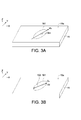
- FIG. 3A schematically illustrates a spatial relationship between the organic molecule in the light emitting layer and a light discharge plane according to the first embodiment of the disclosure.
- FIG. 3B schematically illustrates a spatial relationship between the dipole moment in the light emitting layer and a light discharge plane according to the first embodiment of the disclosure. It is assumed that the light discharge plane of the embodiment is the top surface 15a of the dipole controlled organic light emitting layer 15 facing the first electrode 11.
- the organic molecule 151 leans to the top surface 15a of the dipole controlled organic light emitting layer 15 at an angle of ⁇ m.
- the dipole moment 153 leans to the top surface 15a of the dipole controlled organic light emitting layer 15 at an angle of ⁇ d .
- the organic molecules 151 of the dipole controlled organic light emitting layer 15 can be anisotropically oriented, and the organic molecules 151 is leaned toward to the light discharge plane of the OLED for decreasing the possibility of exciton energy directly coupled into the second electrode 12 (ex: cathode). Please refer to FIG. 1, FIG. 2A and FIG. 3A .
- the longest axes, Mx, of the anisotropically oriented organic molecules 151 of the organic light emitting material of the dipole controlled organic light emitting layer 15 are substantially oriented within an angular range from 0 to less than 45 degrees with respect to an extending direction of the first electrode 11 and an extending direction of a light discharge plane (i.e.
- the longest axes, Mx, of the anisotropically oriented organic molecules 151 are substantially oriented within an angular range from 0 to 15 degrees with respect to an extending direction of the first electrode 11 and an extending direction of a light discharge plane (i.e. the top surface 15a) of the OLED (0 degree ⁇ m ⁇ 15 degrees). It is more ideally that the longest axes, Mx, of the anisotropically oriented organic molecules 151 of the first embodiment are substantially parallel to the first electrode 11 and the light discharge plane (i.e. the top surface 15a) of the OLED.
- the exciton dipole moments 153 in the dipole controlled organic light emitting layer 15 can be anisotropically oriented, and the exciton dipole moments 153 is leaned toward to the light discharge plane of the OLED for decreasing the possibility of exciton energy directly coupled into the second electrode 12 (ex: cathode).
- the directions of the dipole moments 153, Dx, of the dipole controlled organic light emitting layer 15 are substantially oriented within an angular range from 0 to less than 45 degrees with respect to an extending direction of the first electrode 11 and an extending direction of a light discharge plane (i.e. the top surface 15a) of the OLED (0 degree ⁇ d ⁇ 45 degrees).
- the directions of the dipole moments 153, Dx, of the organic molecules 151 are substantially oriented within an angular range from 0 to 15 degrees with respect to an extending direction of the first electrode 11 and an extending direction of the light discharge plane of the OLED (0 degree ⁇ d ⁇ 15 degrees). It is more ideally that the directions of the dipole moments 153, Dx, of the dipole controlled organic light emitting layer 15 of the first embodiment are substantially parallel to the first electrode 11 and the light discharge plane (i.e. top surface 15a) of the OLED.
- an angle ( ⁇ m ) of the longest axes of the organic molecules 151 with respect to an extending direction of the first electrode 11 can be equal to an angle ( ⁇ d ) of said exciton dipole moments 153 of the organic molecules 151 with respect to the extending direction of the first electrode 11.
- an angle ( ⁇ m ) of the longest axes of the organic molecules 151 with respect to an extending direction of the first electrode 11 can be different from an angle ( ⁇ d ) of said exciton dipole moments 153 of the organic molecules 151 with respect to the extending direction of the first electrode 11, which means an angle exists between the exciton dipole moments 153 and the longest axes of the organic molecules 151.
- the organic molecules 151 of the organic light emitting material or the dipole moments 153 of the organic light emitting layer 15 exhibit an orderly arrangement such as anisotropically arranged, in order to prevent exciton energy from transferring into the SPP (surface plasmon polariton) mode, thereby decreasing the possibility of exciton energy directly coupled into the cathode.
- Low SPP mode is one of key factors of high light efficiency of an OLED.
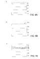
- FIG. 4A ⁇ FIG. 4F schematically show top views of some applicable anisotropic arrangements of the organic molecules of the organic light emitting layer according to the embodiment.
- the longest axes (Mx) of the organic molecules 151 of the organic light emitting material can be anisotropically arranged as an array of matrix, from the top view of the OLED.
- the longest axes (Mx) of the organic molecules 151 of the organic light emitting material can be anisotropically arranged as a pattern with columns in parallel, and the organic molecules 151 in adjacent rows are staggered.
- the longest axes (Mx) of the organic molecules 151 of the organic light emitting material can be anisotropically arranged as a pattern with rows in parallel, and the organic molecules 151 in adjacent columns are staggered.
- the longest axes (Mx) of the organic molecules 151 of the organic light emitting material can be anisotropically arranged as a radiation pattern. As shown in FIG. 4D , a radiation center of the radiation pattern is substantially positioned adjacent to or closed to a corner of the light emitting layer, such as adjacent to the left downward corner of the dipole controlled organic light emitting layer 15. Alternatively, a radiation center of the radiation pattern is substantially positioned adjacent to or closed to a center of the light emitting layer, as shown in FIG. 4E . Additionally, the longest axes (Mx) of the organic molecules 151 of the organic light emitting material can be anisotropically arranged as a spiral pattern, as shown in FIG. 4F .
- the dipole moments 153 of the embodiment can exhibit the anisotropic arrangements as exemplified by a pattern with rows in parallel, a pattern with columns in parallel, an array of matrix, a radiation pattern, a spiral pattern in respective FIG. 4A ⁇ FIG. 4F , or the like.
- FIG. 4A ⁇ FIG. 4F are not all the applicable anisotropic arrangements of the organic molecules 151 and/or the dipole moments 153 in the embodiment.
- Other anisotropic arrangements would be applicable, and could be modified and changed optionally according to the design conditions of the application.
- the present disclosure is not limited to those configurations
- the anisotropic orientation of the organic molecules 151 and/or the dipole moments 153 can be formed by applying an action at a distance, such as providing a magnetic field or an electrical field in the procedures of fabricating the dipole controlled organic light emitting layer 15.
- the organic molecules 151 can be anisotropically oriented by introducing a magnetic field or an electrical field to the environment for depositing, coating or material mixing of the organic light emitting layer 15.
- FIG. 5A schematically shows a cross-sectional view of an organic light emitting device with isotropically oriented organic molecules.
- the distribution of the organic molecules 151 are directionally independent.
- FIG. 5B schematically shows a cross-sectional view of an organic light emitting device with anisotropically oriented organic molecules according to the first embodiment of the disclosure.
- the distribution of the organic molecules 151 are directionally dependent.
- the organic molecules 151 are isotropically oriented ( FIG. 5A ) before applying a magnetic field or an electrical field in the fabricating procedures of the organic light emitting layer 15, and would be anisotropically oriented after action of the magnetic or electrical field on the organic light emitting layer 15.
- the organic molecules 151 and/or the dipole moments 153 of the embodiment would be anisotropic permanently.
- FIG. 6 schematically shows a cross-sectional view of an electric field acting on an organic light emitting device according to the first embodiment of the disclosure.
- an action at a distance such as an electrical field as shown in FIG. 6 or a magnetic field, is applied for inducing the anisotropic orientation of the organic molecules 151 and/or the dipole moments 153 of the dipole controlled organic light emitting layer 15.
- the anisotropic orientation of the organic molecules 151 and/or the dipole moments 153 are not existed permanently, and only presented when the OLED is operated.
- the isotropically oriented organic molecules 151 before OLED operation can be referred to the illustration of FIG. 5A
- the anisotropically oriented organic molecules 151 after OLED operation can be referred to the illustration of FIG. 5B .
- anisotropically oriented the organic molecules 151 and/or the dipole moments 153 of the embodiment can be presented before or after the OLED operation, and the present disclosure has no particular limitation thereto.
- FIG. 7 schematically shows a cross-sectional view of an organic light emitting device according to the second embodiment of the disclosure.
- Identical elements of the second and the first embodiments, such as the substrate 10, the first electrode 11, and the second electrode 12, are designated with the same reference numerals, and details of the same elements described in the first embodiment are not redundantly repeated herein.
- an OLED 2 at least comprises a first electrode 11 and a second electrode 12 disposed oppositely, an organic light emitting layer 25 formed between the first electrode 11 and the second electrode 12, and a periodic array of nano-grating structure 26 formed between the first electrode 11 and the second electrode 12.
- the periodic array of nano-grating structure 26 can be, but not limitedly, formed in the organic light emitting layer 25, as depicted in FIG. 7 .
- the periodic array of nano-grating structure 26 as shown in FIG. 7 functions as a structure of photonic crystals. It is noted that the present disclosure is not limited to the configuration of FIG. 7 . Other periodic arrays resulting in a photonic bandgap able to block the TM polarized light are also applicable in the OLED of the second embodiment.
- the propagating direction of TM polarized light is parallel to the extending direction of the first electrode 11, or parallel to the extending direction of a light discharge plane (ex: to surface of organic light emitting layer 25) of the OLED.
- the propagating direction of TE polarized light is perpendicular to the extending direction of the first electrode, or perpendicular to the extending direction of the light discharge plane of the OLED.
- the periodic array of nano-grating structure 26 is a periodic array resulting in a photonic bandgap, and a range of frequency within which a specific wavelength of light, such as TM polarized light can be blocked.
- the periodic array of nano-grating structure 26 in the organic light emitting layer 25 allows TE polarized light to propagate into the periodic array (photonic crystals) and through the organic light emitting layer 25, but inhibits even prevents the propagation of the TM polarized light.
- the ratio of TM polarization to TE polarization is significantly decreased.
- the ratio of TM polarization to TE polarization is about 0.1 or less. Less or no TE polarized light is generated and/or propagated, and the possibility of exciton energy of TE polarized light coupled into the cathode (ex: the second electrode 12) is decreased consequently, Thus, the light efficiency of the OLED of the second embodiment can be significantly improved.
- an organic light emitting layer of an organic light emitting device may comprise the periodic array of nano-grating structure 26 as described in the second embodiment, and the anisotropically oriented organic molecules 151 and/or dipole moments 153 as described in the first embodiment, to ensure the decrease of the possibility of exciton energy coupled into the cathode.
- FIG. 8 schematically illustrates a cross-sectional view of an organic light emitting device according to the third embodiment of the disclosure.
- Identical elements of the third and the first embodiments, such as the substrate 10, the first electrode 11, and the second electrode 12, are designated with the same reference numerals, and details of the same elements described in the first embodiment are not redundantly repeated herein.
- an OLED further comprises an electron-transporting layer (ETL) formed between the second electrode (ex: cathode) 12 and the organic light emitting layer 35.
- ETL electron-transporting layer
- the organic light emitting layer 35 could be the dipole controlled organic light emitting layer 15 comprising anisotropically oriented organic molecules 151 and/or dipole moments 153 as described in the first embodiment, or the periodic array of nano-grating structure 26 as described in the second embodiment, or both.
- an OLED 3 may comprise the first electrode (ex: anode) 11 formed on the substrate 10, a hole-injecting layer (HIL) formed on the first electrode 11, a hole-transporting layer (HTL) formed on the HIL, the organic light emitting layer 35 formed on the HTL, an electron-transporting layer (ETL) formed on the organic light emitting layer 35, wherein the organic light emitting layer 35 is positioned between the second electrode 12 and the ETL.
- HIL hole-injecting layer
- HTL hole-transporting layer
- ETL electron-transporting layer
- the ETL has a thickness in a range of about 2nm to about 200nm.
- the electron-transporting layer is formed between the second electrode (ex: cathode) and the organic light emitting layer 35 for further decreasing the possibility of exciton energy coupled into the cathode, thereby achieving a higher light efficiency of the embodied OLED.
- FIG. 9A and FIG. 9B schematically illustrate cross-sectional views of two organic light emitting devices according to the fourth embodiment of the disclosure.
- Identical elements of the fourth and the first embodiments such as the substrate 10, the first electrode 11, and the second electrode 12, are designated with the same reference numerals, and details of the same elements described in the first embodiment are not redundantly repeated herein.
- the organic light emitting layer 35 of the fourth embodiment could be the dipole controlled organic light emitting layer 15 comprising anisotropically oriented organic molecules 151 and/or dipole moments 153 as described in the first embodiment, or the periodic array of nano-grating structure 26 as described in the second embodiment, or both.
- a side of the substrate 10 opposite to the first electrode 11 may have a light dispersion surface, by laminating an extra light dispersion layer 17 on the substrate 10 ( FIG. 9A ) or patterning one surface of the substrate 10' to form a light dispersion plane 101 ( FIG. 9B ).
- an OLED further comprises a light dispersion layer 17 laminated on one side of the substrate 10 opposite to the first electrode 11 for guiding the light emitted from the organic light emitting layer 35 upwardly.
- the light dispersion layer 17 comprises an array of micro-optical components.
- the array of micro-optical components is a periodic pattern such as an array of micro lens, or micro bumps, or micro pillars or the like.
- the light dispersion layer 17 makes it possible to take out a greater amount of light.
- the light dispersion layer 17 can be made from a material different from the substrate 10.
- a refractive index of the light dispersion layer 17 is higher than a refractive index of the substrate 10 to ensure the light to be discharged out of the device efficiently.
- one side of the substrate 10' is a light dispersion plane 101 comprising a plurality of micro-optical components.
- the micro-optical components can be configured as an array of micro lens or micro bumps, or micro pillars or the like.
- the light dispersion plane 101 of the substrate 10' guides the light emitted from the organic light emitting layer 35 upwardly, which makes it possible to take out a greater amount of light.
- FIG. 10 schematically illustrates a cross-sectional view of an organic light emitting device according to the fifth embodiment of the disclosure.
- Identical elements of the fifth and the first/fourth embodiments, such as the substrate 10, the first electrode 11, and the second electrode 12, are designated with the same reference numerals, and details are not redundantly repeated herein.
- the organic light emitting layer 35 of the fifth embodiment could be the dipole controlled organic light emitting layer 15 comprising anisotropically oriented organic molecules 151 and/or dipole moments 153 as described in the first embodiment, or the periodic array of nano-grating structure 26 as described in the second embodiment, or both.
- an OLED 5 further comprises an intermediate layer 18 disposed between the substrate 10 and the first electrode 11, and a plurality of light-scattering particles 181 are distributed in the intermediate layer 18 for scattering light.
- the light-scattering particles 181 distributed in the intermediate layer 18 help to guide the light emitted from the organic light emitting layer 35 upwardly, which also makes it possible to take out a greater amount of light.
- a substrate with a high refractive index can be adopted in the OLED of the embodiment, to ensure the light to be discharged out of the device efficiently.
- a substrate 10/10' of an embodied OLED has a high refractive index higher than that of the first electrode 11.
- a substrate 10/10' of an embodied OLED has a high refractive index n larger than 1.5, such as in a range of larger than 1.5 to 2.0.
- the first electrode 11 can be an ITO having a refractive index of about 1.9, and the substrate 10 having a refractive index of larger than about 1.5.
- a substrate 10/10' of an embodied OLED has a high refractive index n equal to or larger than 1.9.
- an organic light emitting device (OLED) of the embodiment could comprise an organic light emitting layer with anisotropically oriented organic molecules or dipole moments (to form a dipole controlled organic light emitting layer), and/or with a periodic array of nano-grating structure (ex: functioning as photonic crystals) contained inside, or both.
- the organic molecules of the organic light emitting material or the dipole moments of the organic light emitting layer exhibit an orderly arrangement such as anisotropically arranged, in order to prevent exciton energy from transferring into the SPP mode, thereby decreasing the possibility of exciton energy directly coupled into the cathode.
- the periodic array of nano-grating structure between the first and second electrodes inhibits generation and propagation of TM polarized light in the organic light emitting layer.
- it is capable of decreasing the possibility of exciton energy directly coupled into the cathode.
- the light efficiency of the OLED can be significantly increased.
Landscapes
- Physics & Mathematics (AREA)
- Optics & Photonics (AREA)
- Electroluminescent Light Sources (AREA)
Abstract
Description
- The disclosure relates in general to an organic light emitting device, and more particularly to an organic light emitting device with improved light efficiency.
- An organic light emitting device, also called an OLED, are attractive because of their low drive voltage, high luminance, wide viewing angle, and capability for full color flat emission displays and for other applications. Also, OLED is capable of providing the full spectrum light which is closest to natural lighting. With those special properties, OLED has become increasingly interesting technology for lighting applications, among other applications.
- Notwithstanding all the developments made in the OLED field, there are more continuing needs for OLED devices that provide higher light efficiency. Low SPP (surface plasmon polariton) mode is one of key factors of high light efficiency of an OLED. The less the exciton energy is coupled into the cathode, the more light the OLED discharges.
- The disclosure is directed to an organic light emitting device, which is designed for decreasing the possibility of exciton energy directly coupled into the cathode or the possibility of propagation of the TM polarized light, thereby significantly increasing the light efficiency of the OLED.
- According to one embodiment, an organic light emitting device (OLED) is provided, comprising a first electrode and a second electrode disposed oppositely, and a dipole controlled organic light emitting layer formed between the first electrode and the second electrode. The dipole controlled organic light emitting layer comprises at least one organic light emitting material, and longest axes of organic molecules of the organic light emitting material are arranged as an anisotropic array.
- In one embodiment, an organic light emitting device (OLED) may further comprises a periodic array of nano-grating structure formed between the first electrode and the second electrode.
- According to another embodiment, an organic light emitting device (OLED) is provided, comprising a first electrode and a second electrode disposed oppositely, and a dipole controlled organic light emitting layer formed between the first electrode and the second electrode. The dipole controlled organic light emitting layer comprises at least one organic light emitting material, and exciton dipole moments of the organic molecules of the organic light emitting material in the dipole controlled organic light emitting layer are anisotropic.
-
-
FIG. 1 schematically shows a cross-sectional view of an organic light emitting device according to the first embodiment of the disclosure. -
FIG. 2A illustrates a coordinate system defining the spatial relationship of the organic molecule skeleton axes in the light emitting layer. -
FIG. 2B illustrate a coordinate system defining the spatial relationship of the exciton dipole moment in the light emitting layer. -
FIG. 3A schematically illustrates a spatial relationship between the organic molecule in the light emitting layer and a light discharge plane according to the first embodiment of the disclosure. -
FIG. 3B schematically illustrates a spatial relationship between the dipole moment in the light emitting layer and a light discharge plane according to the first embodiment of the disclosure. -
FIG. 4A ~ FIG. 4F schematically show top views of some applicable anisotropic arrangements of the organic molecules of the organic light emitting layer according to the embodiment. -
FIG. 5A schematically shows a cross-sectional view of an organic light emitting device with isotropically oriented organic molecules. -
FIG. 5B schematically shows a cross-sectional view of an organic light emitting device with anisotropically oriented organic molecules according to the first embodiment of the disclosure. -
FIG. 6 schematically shows a cross-sectional view of an electric field acting on an organic light emitting device according to the first embodiment of the disclosure. -
FIG. 7 schematically shows a cross-sectional view of an organic light emitting device according to the second embodiment of the disclosure. -
FIG. 8 schematically illustrates a cross-sectional view of an organic light emitting device according to the third embodiment of the disclosure. -
FIG. 9A and FIG. 9B schematically illustrate cross-sectional views of two organic light emitting devices according to the fourth embodiment of the disclosure. -
FIG. 10 schematically illustrates a cross-sectional view of an organic light emitting device according to the fifth embodiment of the disclosure. - In the following detailed description, for purposes of explanation, numerous specific details are set forth in order to provide a thorough understanding of the disclosed embodiments. It will be apparent, however, that one or more embodiments may be practiced without these specific details. In other instances, well-known structures and devices are schematically shown in order to simplify the drawing.
- Below, exemplary embodiments of organic light emitting devices will be described in detail with reference to accompanying drawings so as to be easily realized by a person having ordinary knowledge in the art. The inventive concept may be embodied in various forms without being limited to the exemplary embodiments set forth herein. Descriptions of well-known parts are omitted for clarity, and like reference numerals refer to like elements throughout.
- In the embodiments, the organic light emitting device (OLED) with particular designs, such as the OLEDs having the dipole controlled organic light emitting layers (with anisotropically oriented organic molecules or dipole moments) and/or a periodic array of nano-grating structure (functioning as photonic crystals inside) between the opposite electrodes of the device (such as formed in the organic light emitting layer), are provided hereinafter for illustrations. According to the structural designs of the embodiments, it is capable of decreasing the possibility of exciton energy directly coupled into the cathode greatly, and/or decreasing the possibility of propagation of the TM polarized light. Thus, the light efficiency of the OLED can be significantly increased.
- Embodiments are provided hereinafter with reference to the accompanying drawings for describing the related configurations and procedures, but the present disclosure is not limited thereto. It is noted that not all embodiments of the invention are shown. Structures of the embodiments would be different, and could be modified and changed optionally according to the design needs of the application. Modifications and variations can be made without departing from the spirit of the disclosure to meet the requirements of the practical applications. Thus, there may be other embodiments of the present disclosure which are not specifically illustrated. It is also important to point out that the illustrations may not be necessarily be drawn to scale. Thus, the specification and the drawings are to be regard as an illustrative sense rather than a restrictive sense.
-
FIG. 1 schematically shows a cross-sectional view of an organic light emitting device according to the first embodiment of the disclosure. According to the first embodiment, an OLED 1 at least comprises afirst electrode 11 and asecond electrode 12 disposed oppositely, and a dipole controlled organiclight emitting layer 15 formed between thefirst electrode 11 and thesecond electrode 12. In the OLED of the embodiment, thefirst electrode 11 can be an anode formed on asubstrate 10, while thesecond electrode 12 can be a cathode formed on the dipole controlled organiclight emitting layer 15. The dipole controlled organiclight emitting layer 15 comprises at least one organic light emitting material (usually two or more different organic lighting materials), and the organic light emitting material comprises a great number oforganic molecules 151. - In the first embodiment, the longest axes of
organic molecules 151 of the organic light emitting material are arranged as an anisotropic array. Alternatively,exciton dipole moments 153 of theorganic molecules 151 in the dipole controlled organiclight emitting layer 15 of the first embodiment are anisotropic, before or after the OLED operation. -
FIG. 2A illustrates a coordinate system defining the spatial relationship of the organic molecule skeleton axes in the light emitting layer.FIG. 2B illustrate a coordinate system defining the spatial relationship of the exciton dipole moment in the light emitting layer. In the dipole controlled organiclight emitting layer 15, the orientational axes of theorganic molecule 151 of the organic light emitting material can be defined as Mx, My and Mz. As shown inFIG. 2A , the direction of the longest axis (or major axis) of theorganic molecule 151 is Mx, and the direction of the short axis (or minor axis) of theorganic molecule 151 is My. The remaining axis of theorganic molecule 151 on the left hand side in the direction vertical to the Mx and My axes is the Mz axis. Also, the direction of thedipole moment 153 of the light emission is along the Dx axis, and the direction vertical to the Dx axis where light is radiated most heavily is along the Dz axis. The remaining axis on the left hand side in the direction vertical to the Dx and Dz axes is the Dy axis. -
FIG. 3A schematically illustrates a spatial relationship between the organic molecule in the light emitting layer and a light discharge plane according to the first embodiment of the disclosure.FIG. 3B schematically illustrates a spatial relationship between the dipole moment in the light emitting layer and a light discharge plane according to the first embodiment of the disclosure. It is assumed that the light discharge plane of the embodiment is thetop surface 15a of the dipole controlled organiclight emitting layer 15 facing thefirst electrode 11. InFIG. 3A , theorganic molecule 151 leans to thetop surface 15a of the dipole controlled organiclight emitting layer 15 at an angle of θm. InFIG. 3B , thedipole moment 153 leans to thetop surface 15a of the dipole controlled organiclight emitting layer 15 at an angle of θd. - The
organic molecules 151 of the dipole controlled organiclight emitting layer 15 can be anisotropically oriented, and theorganic molecules 151 is leaned toward to the light discharge plane of the OLED for decreasing the possibility of exciton energy directly coupled into the second electrode 12 (ex: cathode). Please refer toFIG. 1, FIG. 2A andFIG. 3A . In one embodiment, the longest axes, Mx, of the anisotropically orientedorganic molecules 151 of the organic light emitting material of the dipole controlled organiclight emitting layer 15 are substantially oriented within an angular range from 0 to less than 45 degrees with respect to an extending direction of thefirst electrode 11 and an extending direction of a light discharge plane (i.e. thetop surface 15a) of the OLED (0 degree <θm < 45 degrees). The extending direction of the light discharge plane is parallel to the xy-plane. In one embodiment, the longest axes, Mx, of the anisotropically orientedorganic molecules 151 are substantially oriented within an angular range from 0 to 15 degrees with respect to an extending direction of thefirst electrode 11 and an extending direction of a light discharge plane (i.e. thetop surface 15a) of the OLED (0 degree ≤θm ≤ 15 degrees). It is more ideally that the longest axes, Mx, of the anisotropically orientedorganic molecules 151 of the first embodiment are substantially parallel to thefirst electrode 11 and the light discharge plane (i.e. thetop surface 15a) of the OLED. - Alternatively, the
exciton dipole moments 153 in the dipole controlled organiclight emitting layer 15 can be anisotropically oriented, and theexciton dipole moments 153 is leaned toward to the light discharge plane of the OLED for decreasing the possibility of exciton energy directly coupled into the second electrode 12 (ex: cathode). Please refer toFIG. 1, FIG. 2B andFIG. 3B . In one embodiment, the directions of thedipole moments 153, Dx, of the dipole controlled organiclight emitting layer 15 are substantially oriented within an angular range from 0 to less than 45 degrees with respect to an extending direction of thefirst electrode 11 and an extending direction of a light discharge plane (i.e. thetop surface 15a) of the OLED (0 degree ≤θd < 45 degrees). In one embodiment, the directions of thedipole moments 153, Dx, of theorganic molecules 151 are substantially oriented within an angular range from 0 to 15 degrees with respect to an extending direction of thefirst electrode 11 and an extending direction of the light discharge plane of the OLED (0 degree ≤θd ≤ 15 degrees). It is more ideally that the directions of thedipole moments 153, Dx, of the dipole controlled organiclight emitting layer 15 of the first embodiment are substantially parallel to thefirst electrode 11 and the light discharge plane (i.e.top surface 15a) of the OLED. - In one embodiment, an angle (θm) of the longest axes of the
organic molecules 151 with respect to an extending direction of thefirst electrode 11 can be equal to an angle (θd) of saidexciton dipole moments 153 of theorganic molecules 151 with respect to the extending direction of thefirst electrode 11. In alternative embodiment, an angle (θm) of the longest axes of theorganic molecules 151 with respect to an extending direction of thefirst electrode 11 can be different from an angle (θd) of saidexciton dipole moments 153 of theorganic molecules 151 with respect to the extending direction of thefirst electrode 11, which means an angle exists between theexciton dipole moments 153 and the longest axes of theorganic molecules 151. - According to the embodiment, the
organic molecules 151 of the organic light emitting material or thedipole moments 153 of the organiclight emitting layer 15 exhibit an orderly arrangement such as anisotropically arranged, in order to prevent exciton energy from transferring into the SPP (surface plasmon polariton) mode, thereby decreasing the possibility of exciton energy directly coupled into the cathode. Low SPP mode is one of key factors of high light efficiency of an OLED. There are a variety of orderly arrangements for anisotropic orientation of theorganic molecules 151 and/or thedipole moments 153 in the applications.FIG. 4A ~ FIG. 4F schematically show top views of some applicable anisotropic arrangements of the organic molecules of the organic light emitting layer according to the embodiment. - As shown in
FIG. 4A , the longest axes (Mx) of theorganic molecules 151 of the organic light emitting material can be anisotropically arranged as an array of matrix, from the top view of the OLED. As shown inFIG. 4B , the longest axes (Mx) of theorganic molecules 151 of the organic light emitting material can be anisotropically arranged as a pattern with columns in parallel, and theorganic molecules 151 in adjacent rows are staggered. As shown inFIG. 4C , the longest axes (Mx) of theorganic molecules 151 of the organic light emitting material can be anisotropically arranged as a pattern with rows in parallel, and theorganic molecules 151 in adjacent columns are staggered. Also, the longest axes (Mx) of theorganic molecules 151 of the organic light emitting material can be anisotropically arranged as a radiation pattern. As shown inFIG. 4D , a radiation center of the radiation pattern is substantially positioned adjacent to or closed to a corner of the light emitting layer, such as adjacent to the left downward corner of the dipole controlled organiclight emitting layer 15. Alternatively, a radiation center of the radiation pattern is substantially positioned adjacent to or closed to a center of the light emitting layer, as shown inFIG. 4E . Additionally, the longest axes (Mx) of theorganic molecules 151 of the organic light emitting material can be anisotropically arranged as a spiral pattern, as shown inFIG. 4F . - Similarly, the
dipole moments 153 of the embodiment can exhibit the anisotropic arrangements as exemplified by a pattern with rows in parallel, a pattern with columns in parallel, an array of matrix, a radiation pattern, a spiral pattern in respectiveFIG. 4A ~ FIG. 4F , or the like. Noted thatFIG. 4A ~ FIG. 4F are not all the applicable anisotropic arrangements of theorganic molecules 151 and/or thedipole moments 153 in the embodiment. Other anisotropic arrangements would be applicable, and could be modified and changed optionally according to the design conditions of the application. Thus, the present disclosure is not limited to those configurations - According to the embodiment, the anisotropic orientation of the
organic molecules 151 and/or thedipole moments 153 can be formed by applying an action at a distance, such as providing a magnetic field or an electrical field in the procedures of fabricating the dipole controlled organiclight emitting layer 15. For example, theorganic molecules 151 can be anisotropically oriented by introducing a magnetic field or an electrical field to the environment for depositing, coating or material mixing of the organiclight emitting layer 15. -
FIG. 5A schematically shows a cross-sectional view of an organic light emitting device with isotropically oriented organic molecules. InFIG. 5A , the distribution of theorganic molecules 151 are directionally independent.FIG. 5B schematically shows a cross-sectional view of an organic light emitting device with anisotropically oriented organic molecules according to the first embodiment of the disclosure. InFIG. 5B , the distribution of theorganic molecules 151 are directionally dependent. In one embodiment, theorganic molecules 151 are isotropically oriented (FIG. 5A ) before applying a magnetic field or an electrical field in the fabricating procedures of the organiclight emitting layer 15, and would be anisotropically oriented after action of the magnetic or electrical field on the organiclight emitting layer 15. After the fabrication of the organiclight emitting layer 15 is done, theorganic molecules 151 and/or thedipole moments 153 of the embodiment would be anisotropic permanently. - Alternatively, the anisotropic orientation of the
organic molecules 151 and/or thedipole moments 153 can be formed during the OLED operation.FIG. 6 schematically shows a cross-sectional view of an electric field acting on an organic light emitting device according to the first embodiment of the disclosure. During operation of OLED, an action at a distance, such as an electrical field as shown inFIG. 6 or a magnetic field, is applied for inducing the anisotropic orientation of theorganic molecules 151 and/or thedipole moments 153 of the dipole controlled organiclight emitting layer 15. In this case, the anisotropic orientation of theorganic molecules 151 and/or thedipole moments 153 are not existed permanently, and only presented when the OLED is operated. Similarly, the isotropically orientedorganic molecules 151 before OLED operation can be referred to the illustration ofFIG. 5A , while the anisotropically orientedorganic molecules 151 after OLED operation can be referred to the illustration ofFIG. 5B . - Thus, anisotropically oriented the
organic molecules 151 and/or thedipole moments 153 of the embodiment can be presented before or after the OLED operation, and the present disclosure has no particular limitation thereto. -
FIG. 7 schematically shows a cross-sectional view of an organic light emitting device according to the second embodiment of the disclosure. Identical elements of the second and the first embodiments, such as thesubstrate 10, thefirst electrode 11, and thesecond electrode 12, are designated with the same reference numerals, and details of the same elements described in the first embodiment are not redundantly repeated herein. - In the second embodiment, an
OLED 2 at least comprises afirst electrode 11 and asecond electrode 12 disposed oppositely, an organiclight emitting layer 25 formed between thefirst electrode 11 and thesecond electrode 12, and a periodic array of nano-gratingstructure 26 formed between thefirst electrode 11 and thesecond electrode 12. In one embodiment, the periodic array of nano-gratingstructure 26 can be, but not limitedly, formed in the organiclight emitting layer 25, as depicted inFIG. 7 . In one embodiment, the periodic array of nano-gratingstructure 26 as shown inFIG. 7 functions as a structure of photonic crystals. It is noted that the present disclosure is not limited to the configuration ofFIG. 7 . Other periodic arrays resulting in a photonic bandgap able to block the TM polarized light are also applicable in the OLED of the second embodiment. - Generally, the propagating direction of TM polarized light is parallel to the extending direction of the
first electrode 11, or parallel to the extending direction of a light discharge plane (ex: to surface of organic light emitting layer 25) of the OLED. The propagating direction of TE polarized light is perpendicular to the extending direction of the first electrode, or perpendicular to the extending direction of the light discharge plane of the OLED. For an OLED of the second embodiment, the periodic array of nano-gratingstructure 26 is a periodic array resulting in a photonic bandgap, and a range of frequency within which a specific wavelength of light, such as TM polarized light can be blocked. Therefore, the periodic array of nano-gratingstructure 26 in the organiclight emitting layer 25 according to the second embodiment allows TE polarized light to propagate into the periodic array (photonic crystals) and through the organiclight emitting layer 25, but inhibits even prevents the propagation of the TM polarized light. - In the second embodiment, since the periodic array of nano-grating
structure 26 in the organiclight emitting layer 25 inhibits and/or prevents the propagation of the TM polarized light, more light energy would be saved for TE polarization. Therefore, the ratio of TM polarization to TE polarization is significantly decreased. In one embodiment, the ratio of TM polarization to TE polarization is about 0.1 or less. Less or no TE polarized light is generated and/or propagated, and the possibility of exciton energy of TE polarized light coupled into the cathode (ex: the second electrode 12) is decreased consequently, Thus, the light efficiency of the OLED of the second embodiment can be significantly improved. - In an alternative embodiment, an organic light emitting layer of an organic light emitting device may comprise the periodic array of nano-grating
structure 26 as described in the second embodiment, and the anisotropically orientedorganic molecules 151 and/ordipole moments 153 as described in the first embodiment, to ensure the decrease of the possibility of exciton energy coupled into the cathode. -
FIG. 8 schematically illustrates a cross-sectional view of an organic light emitting device according to the third embodiment of the disclosure. Identical elements of the third and the first embodiments, such as thesubstrate 10, thefirst electrode 11, and thesecond electrode 12, are designated with the same reference numerals, and details of the same elements described in the first embodiment are not redundantly repeated herein. - In the third embodiment, an OLED further comprises an electron-transporting layer (ETL) formed between the second electrode (ex: cathode) 12 and the organic
light emitting layer 35. The organiclight emitting layer 35 could be the dipole controlled organiclight emitting layer 15 comprising anisotropically orientedorganic molecules 151 and/ordipole moments 153 as described in the first embodiment, or the periodic array of nano-gratingstructure 26 as described in the second embodiment, or both. - Besides the ETL, other layers typically adopted in the OLED could be constructed optionally, but not limitedly. As shown in
FIG. 8 , anOLED 3 may comprise the first electrode (ex: anode) 11 formed on thesubstrate 10, a hole-injecting layer (HIL) formed on thefirst electrode 11, a hole-transporting layer (HTL) formed on the HIL, the organiclight emitting layer 35 formed on the HTL, an electron-transporting layer (ETL) formed on the organiclight emitting layer 35, wherein the organiclight emitting layer 35 is positioned between thesecond electrode 12 and the ETL. - In one embodiment, the ETL has a thickness in a range of about 2nm to about 200nm.
- According to the third embodiment, the electron-transporting layer (ETL) is formed between the second electrode (ex: cathode) and the organic
light emitting layer 35 for further decreasing the possibility of exciton energy coupled into the cathode, thereby achieving a higher light efficiency of the embodied OLED. -
FIG. 9A and FIG. 9B schematically illustrate cross-sectional views of two organic light emitting devices according to the fourth embodiment of the disclosure. Identical elements of the fourth and the first embodiments, such as thesubstrate 10, thefirst electrode 11, and thesecond electrode 12, are designated with the same reference numerals, and details of the same elements described in the first embodiment are not redundantly repeated herein. Similarly, the organiclight emitting layer 35 of the fourth embodiment could be the dipole controlled organiclight emitting layer 15 comprising anisotropically orientedorganic molecules 151 and/ordipole moments 153 as described in the first embodiment, or the periodic array of nano-gratingstructure 26 as described in the second embodiment, or both. - In the fourth embodiment, a side of the
substrate 10 opposite to thefirst electrode 11 may have a light dispersion surface, by laminating an extralight dispersion layer 17 on the substrate 10 (FIG. 9A ) or patterning one surface of the substrate 10' to form a light dispersion plane 101 (FIG. 9B ). - As shown in
FIG. 9A , an OLED further comprises alight dispersion layer 17 laminated on one side of thesubstrate 10 opposite to thefirst electrode 11 for guiding the light emitted from the organiclight emitting layer 35 upwardly. In one embodiment, thelight dispersion layer 17 comprises an array of micro-optical components. The array of micro-optical components is a periodic pattern such as an array of micro lens, or micro bumps, or micro pillars or the like. Thelight dispersion layer 17 makes it possible to take out a greater amount of light. - Also, the
light dispersion layer 17 can be made from a material different from thesubstrate 10. In one embodiment, a refractive index of thelight dispersion layer 17 is higher than a refractive index of thesubstrate 10 to ensure the light to be discharged out of the device efficiently. - As shown in
FIG. 9B , one side of the substrate 10' is alight dispersion plane 101 comprising a plurality of micro-optical components. The micro-optical components can be configured as an array of micro lens or micro bumps, or micro pillars or the like. Similarly, thelight dispersion plane 101 of the substrate 10' guides the light emitted from the organiclight emitting layer 35 upwardly, which makes it possible to take out a greater amount of light. -
FIG. 10 schematically illustrates a cross-sectional view of an organic light emitting device according to the fifth embodiment of the disclosure. Identical elements of the fifth and the first/fourth embodiments, such as thesubstrate 10, thefirst electrode 11, and thesecond electrode 12, are designated with the same reference numerals, and details are not redundantly repeated herein. Similarly, the organiclight emitting layer 35 of the fifth embodiment could be the dipole controlled organiclight emitting layer 15 comprising anisotropically orientedorganic molecules 151 and/ordipole moments 153 as described in the first embodiment, or the periodic array of nano-gratingstructure 26 as described in the second embodiment, or both. - In the fifth embodiment, an
OLED 5 further comprises anintermediate layer 18 disposed between thesubstrate 10 and thefirst electrode 11, and a plurality of light-scatteringparticles 181 are distributed in theintermediate layer 18 for scattering light. According to the fifth embodiment, the light-scatteringparticles 181 distributed in theintermediate layer 18 help to guide the light emitted from the organiclight emitting layer 35 upwardly, which also makes it possible to take out a greater amount of light. - Additionally, a substrate with a high refractive index can be adopted in the OLED of the embodiment, to ensure the light to be discharged out of the device efficiently. In one embodiment, a
substrate 10/10' of an embodied OLED has a high refractive index higher than that of thefirst electrode 11. In one embodiment, asubstrate 10/10' of an embodied OLED has a high refractive index n larger than 1.5, such as in a range of larger than 1.5 to 2.0. In one embodiment, thefirst electrode 11 can be an ITO having a refractive index of about 1.9, and thesubstrate 10 having a refractive index of larger than about 1.5. In one embodiment, asubstrate 10/10' of an embodied OLED has a high refractive index n equal to or larger than 1.9. - According to the aforementioned descriptions, an organic light emitting device (OLED) of the embodiment could comprise an organic light emitting layer with anisotropically oriented organic molecules or dipole moments (to form a dipole controlled organic light emitting layer), and/or with a periodic array of nano-grating structure (ex: functioning as photonic crystals) contained inside, or both. In one of the embodiments, the organic molecules of the organic light emitting material or the dipole moments of the organic light emitting layer exhibit an orderly arrangement such as anisotropically arranged, in order to prevent exciton energy from transferring into the SPP mode, thereby decreasing the possibility of exciton energy directly coupled into the cathode. In one of the embodiments, the periodic array of nano-grating structure between the first and second electrodes (ex: in the organic light emitting layer) inhibits generation and propagation of TM polarized light in the organic light emitting layer. According to the structural designs of the embodiments, it is capable of decreasing the possibility of exciton energy directly coupled into the cathode. Thus, the light efficiency of the OLED can be significantly increased.
- It will be apparent to those skilled in the art that various modifications and variations can be made to the disclosed embodiments. It is intended that the specification and examples be considered as exemplary only, with a true scope of the disclosure being indicated by the following claims and their equivalents.
Claims (15)
- An organic light emitting device, comprising:a first electrode (11) and a second electrode (12) disposed oppositely; anda dipole controlled organic light emitting layer (15), formed between the first electrode and the second electrode, and the dipole controlled organic light emitting layer comprising at least one organic light emitting material, wherein longest axes (Mx) of organic molecules (151) of the organic light emitting material are oriented as an anisotropic array.
- The organic light emitting device according to claim 1, wherein said longest axes of the organic molecules of the organic light emitting material are substantially oriented within an angular range from 0 to 15 degrees with respect to an extending direction of the first electrode.
- The organic light emitting device according to claim 1 or 2, wherein said longest axes of the organic molecules of the organic light emitting material are substantially parallel to the first electrode.
- The organic light emitting device according to any one of claims 1 to 3, wherein said longest axes of the organic molecules of the organic light emitting material are anisotropically oriented as a pattern with rows in parallel, a pattern with columns in parallel, an array of matrix, a radiation pattern, or a spiral pattern.
- The organic light emitting device according to any one of claims 1 to 4, wherein exciton dipole moments of the organic molecules in the dipole controlled organic light emitting layer are anisotropic.
- The organic light emitting device according to claim 5, wherein said exciton dipole moments of the organic molecules in the dipole controlled organic light emitting layer are substantially oriented within an angular range from 0 to 15 degrees with respect to an extending direction of the first electrode.
- The organic light emitting device according to claim 5, wherein said exciton dipole moments of the organic molecules in the dipole controlled organic light emitting layer are substantially parallel to the first electrode.
- The organic light emitting device according to claim 5, wherein said exciton dipole moments of the organic molecules in the dipole controlled organic light emitting layer are anisotropically arranged as a pattern with rows in parallel, a pattern with columns in parallel, an array of matrix, a radiation pattern, or a spiral pattern.
- The organic light emitting device according to claim 5, wherein an angle of said longest axes of the organic molecules with respect to an extending direction of the first electrode is different from an angle of said exciton dipole moments of the organic molecules with respect to the extending direction of the first electrode.
- The organic light emitting device according to any one of claims 1 to 9, wherein the first electrode is formed on a substrate and the second electrode is formed on the dipole controlled organic light emitting layer, and the organic light emitting device further comprises an electron-transporting layer (ETL) formed between the second electrode and the dipole controlled organic light emitting layer, wherein the ETL has a thickness in a range of about 2 nm to about 200 nm.
- The organic light emitting device according to claim 10, wherein the substrate has a high refractive index n equal to or larger than 1.9.
- The organic light emitting device according to claim 10 or 11, further comprising a light dispersion layer laminated on one side of the substrate opposite to the first electrode, wherein the light dispersion layer comprises an array of micro-optical components.
- The organic light emitting device according to any one of claims 10 to 12, wherein one side of the substrate is a light dispersion plane comprising a plurality of micro-optical components
- The organic light emitting device according to any one of claims 10 to 13, further comprising an intermediate layer disposed between the substrate and the first electrode, and a plurality of light-scattering particles distributed in the intermediate layer.
- The organic light emitting device according to any one of claims 1 to 14, further comprising a periodic array of nano-grating structure formed between the first electrode and the second electrode, wherein the periodic array of nano-grating structure inhibits generation and propagation of TM polarized light, and the periodic array of nano-grating structure allows TE polarized light to propagate into the periodic array of nano-grating structure and through the dipole controlled organic light emitting layer.
Applications Claiming Priority (2)
| Application Number | Priority Date | Filing Date | Title |
|---|---|---|---|
| US201361901039P | 2013-11-07 | 2013-11-07 | |
| US14/445,672 US20150200381A1 (en) | 2013-11-07 | 2014-07-29 | Organic light emitting device |
Publications (2)
| Publication Number | Publication Date |
|---|---|
| EP2871687A2 true EP2871687A2 (en) | 2015-05-13 |
| EP2871687A3 EP2871687A3 (en) | 2015-05-27 |
Family
ID=51846540
Family Applications (1)
| Application Number | Title | Priority Date | Filing Date |
|---|---|---|---|
| EP14191817.7A Withdrawn EP2871687A3 (en) | 2013-11-07 | 2014-11-05 | Organic light emitting device |
Country Status (3)
| Country | Link |
|---|---|
| US (1) | US20150200381A1 (en) |
| EP (1) | EP2871687A3 (en) |
| CN (1) | CN104810481A (en) |
Families Citing this family (4)
| Publication number | Priority date | Publication date | Assignee | Title |
|---|---|---|---|---|
| KR102126382B1 (en) * | 2014-02-19 | 2020-06-25 | 삼성디스플레이 주식회사 | Organic light-emitting display apparatus |
| CN107681056B (en) * | 2016-08-01 | 2019-04-30 | 上海和辉光电有限公司 | A kind of manufacturing method and organic luminescent device of organic luminescent device |
| CN109983597B (en) * | 2016-11-29 | 2021-09-07 | 默克专利有限公司 | organic electroluminescent element |
| CN113540186A (en) * | 2021-06-23 | 2021-10-22 | 合肥欣奕华智能机器有限公司 | Anti-peep display panel, display device and preparation method |
Family Cites Families (14)
| Publication number | Priority date | Publication date | Assignee | Title |
|---|---|---|---|---|
| US5677545A (en) * | 1994-09-12 | 1997-10-14 | Motorola | Organic light emitting diodes with molecular alignment and method of fabrication |
| JPH11102783A (en) * | 1997-09-26 | 1999-04-13 | Mitsubishi Electric Corp | Organic electroluminescence device and method of manufacturing the same |
| JP2002110362A (en) * | 2000-09-27 | 2002-04-12 | Seiko Epson Corp | Surface emitting device |
| JP4984343B2 (en) * | 2000-09-29 | 2012-07-25 | 株式会社日立製作所 | Organic electroluminescent device and optoelectronic device using the same |
| US8283679B2 (en) * | 2003-06-30 | 2012-10-09 | Semiconductor Energy Laboratory Co., Ltd. | Semiconductor device having light-emitting element and light-receiving element for transmitting among circuits formed over the plurality of substrates |
| US8134291B2 (en) * | 2005-01-07 | 2012-03-13 | Samsung Mobile Display Co., Ltd. | Electroluminescent device and method for preparing the same |
| JP2006228861A (en) * | 2005-02-16 | 2006-08-31 | Kyoto Univ | Organic electroluminescence device and method for manufacturing the same |
| CN100565968C (en) * | 2005-06-03 | 2009-12-02 | 皇家飞利浦电子股份有限公司 | Organic Electroluminescent Light Source |
| US9219249B2 (en) * | 2010-04-28 | 2015-12-22 | Koninklijke Philips N.V. | Organic light emitting device with increased light out coupling |
| GB201015417D0 (en) * | 2010-09-15 | 2010-10-27 | Lomox Ltd | Organic light emitting diode devices |
| JP5546480B2 (en) * | 2011-03-08 | 2014-07-09 | 株式会社東芝 | Organic electroluminescent device and manufacturing method thereof |
| TW201316584A (en) * | 2011-10-11 | 2013-04-16 | Hon Hai Prec Ind Co Ltd | OLED manufacturing method |
| DE102012203583B4 (en) * | 2012-03-07 | 2021-03-18 | Pictiva Displays International Limited | Organic light-emitting component |
| KR102065904B1 (en) * | 2012-12-07 | 2020-01-15 | 엘지디스플레이 주식회사 | Organic light emitting diode device and liquid crystal type emitting material used for the same |
-
2014
- 2014-07-29 US US14/445,672 patent/US20150200381A1/en not_active Abandoned
- 2014-11-05 EP EP14191817.7A patent/EP2871687A3/en not_active Withdrawn
- 2014-11-06 CN CN201410621008.XA patent/CN104810481A/en active Pending
Non-Patent Citations (1)
| Title |
|---|
| None |
Also Published As
| Publication number | Publication date |
|---|---|
| CN104810481A (en) | 2015-07-29 |
| EP2871687A3 (en) | 2015-05-27 |
| US20150200381A1 (en) | 2015-07-16 |
Similar Documents
| Publication | Publication Date | Title |
|---|---|---|
| Ou et al. | Extremely efficient white organic light‐emitting diodes for general lighting | |
| CN106663740B (en) | OLED device with enhancement layer | |
| Lee et al. | A light scattering layer for internal light extraction of organic light-emitting diodes based on silver nanowires | |
| US10680208B2 (en) | Electroluminescent device and display pixel structure using the same | |
| US20130193416A1 (en) | Organic electroluminescent devices and methods for fabricating the same | |
| US10038159B2 (en) | Organic electroluminescent device structure and manufacturing for the same | |
| US8987767B2 (en) | Light emitting device having improved light extraction efficiency | |
| CN106684256A (en) | Display panel and fabrication method thereof | |
| CN106796948B (en) | Display panel and method for manufacturing the same | |
| EP2884555B1 (en) | OLED on curved substrate | |
| EP2966704B1 (en) | Internal extraction layer for enhanced light outcoupling for oleds | |
| TW201535821A (en) | Organic electroluminescent element, illumination device and display device | |
| US20230157058A1 (en) | Organic electroluminescent devices | |
| CN104659267A (en) | A structure to enhance light extraction and lifetime of oled devices | |
| US20130234590A1 (en) | Display device and method for manufacturing the same | |
| US20150200381A1 (en) | Organic light emitting device | |
| US11106109B2 (en) | Display panel capable of three-axis focal point length conversion | |
| Suh et al. | Preparation of randomly distributed micro-lens arrays fabricated from porous polymer film and their application as a light extraction component | |
| JP2015090810A (en) | El display device, and method of manufacturing el display device | |
| Dong et al. | Multi-mode organic light-emitting diode to suppress the viewing angle dependence | |
| ES2631178T3 (en) | Procedure for manufacturing a surface plasmon wave generating structure | |
| CN105378963B (en) | Opto-electronic device and the method for manufacturing opto-electronic device | |
| Joo et al. | Optical and structural approaches for improved luminance distribution and enhanced efficiency of organic light emitting diodes | |
| US10276821B2 (en) | Electroluminescent device | |
| US12364095B2 (en) | Organic electroluminescent devices |
Legal Events
| Date | Code | Title | Description |
|---|---|---|---|
| PUAL | Search report despatched |
Free format text: ORIGINAL CODE: 0009013 |
|
| PUAI | Public reference made under article 153(3) epc to a published international application that has entered the european phase |
Free format text: ORIGINAL CODE: 0009012 |
|
| 17P | Request for examination filed |
Effective date: 20141105 |
|
| AK | Designated contracting states |
Kind code of ref document: A2 Designated state(s): AL AT BE BG CH CY CZ DE DK EE ES FI FR GB GR HR HU IE IS IT LI LT LU LV MC MK MT NL NO PL PT RO RS SE SI SK SM TR |
|
| AX | Request for extension of the european patent |
Extension state: BA ME |
|
| AK | Designated contracting states |
Kind code of ref document: A3 Designated state(s): AL AT BE BG CH CY CZ DE DK EE ES FI FR GB GR HR HU IE IS IT LI LT LU LV MC MK MT NL NO PL PT RO RS SE SI SK SM TR |
|
| AX | Request for extension of the european patent |
Extension state: BA ME |
|
| RIC1 | Information provided on ipc code assigned before grant |
Ipc: H01L 51/52 20060101ALI20150417BHEP Ipc: H01L 51/50 20060101AFI20150417BHEP |
|
| R17P | Request for examination filed (corrected) |
Effective date: 20151027 |
|
| RBV | Designated contracting states (corrected) |
Designated state(s): AL AT BE BG CH CY CZ DE DK EE ES FI FR GB GR HR HU IE IS IT LI LT LU LV MC MK MT NL NO PL PT RO RS SE SI SK SM TR |
|
| GRAP | Despatch of communication of intention to grant a patent |
Free format text: ORIGINAL CODE: EPIDOSNIGR1 |
|
| INTG | Intention to grant announced |
Effective date: 20170914 |
|
| STAA | Information on the status of an ep patent application or granted ep patent |
Free format text: STATUS: THE APPLICATION IS DEEMED TO BE WITHDRAWN |
|
| 18D | Application deemed to be withdrawn |
Effective date: 20180125 |