EP2869451A1 - Device, method, and program for controlling converter, and air conditioner - Google Patents
Device, method, and program for controlling converter, and air conditioner Download PDFInfo
- Publication number
- EP2869451A1 EP2869451A1 EP13833735.7A EP13833735A EP2869451A1 EP 2869451 A1 EP2869451 A1 EP 2869451A1 EP 13833735 A EP13833735 A EP 13833735A EP 2869451 A1 EP2869451 A1 EP 2869451A1
- Authority
- EP
- European Patent Office
- Prior art keywords
- phase
- voltage
- switching element
- arm switching
- converter
- Prior art date
- Legal status (The legal status is an assumption and is not a legal conclusion. Google has not performed a legal analysis and makes no representation as to the accuracy of the status listed.)
- Granted
Links
Images





Classifications
-
- H—ELECTRICITY
- H02—GENERATION; CONVERSION OR DISTRIBUTION OF ELECTRIC POWER
- H02M—APPARATUS FOR CONVERSION BETWEEN AC AND AC, BETWEEN AC AND DC, OR BETWEEN DC AND DC, AND FOR USE WITH MAINS OR SIMILAR POWER SUPPLY SYSTEMS; CONVERSION OF DC OR AC INPUT POWER INTO SURGE OUTPUT POWER; CONTROL OR REGULATION THEREOF
- H02M1/00—Details of apparatus for conversion
- H02M1/42—Circuits or arrangements for compensating for or adjusting power factor in converters or inverters
- H02M1/4208—Arrangements for improving power factor of AC input
- H02M1/4233—Arrangements for improving power factor of AC input using a bridge converter comprising active switches
-
- H—ELECTRICITY
- H02—GENERATION; CONVERSION OR DISTRIBUTION OF ELECTRIC POWER
- H02M—APPARATUS FOR CONVERSION BETWEEN AC AND AC, BETWEEN AC AND DC, OR BETWEEN DC AND DC, AND FOR USE WITH MAINS OR SIMILAR POWER SUPPLY SYSTEMS; CONVERSION OF DC OR AC INPUT POWER INTO SURGE OUTPUT POWER; CONTROL OR REGULATION THEREOF
- H02M1/00—Details of apparatus for conversion
- H02M1/42—Circuits or arrangements for compensating for or adjusting power factor in converters or inverters
- H02M1/4208—Arrangements for improving power factor of AC input
- H02M1/4216—Arrangements for improving power factor of AC input operating from a three-phase input voltage
-
- H—ELECTRICITY
- H02—GENERATION; CONVERSION OR DISTRIBUTION OF ELECTRIC POWER
- H02M—APPARATUS FOR CONVERSION BETWEEN AC AND AC, BETWEEN AC AND DC, OR BETWEEN DC AND DC, AND FOR USE WITH MAINS OR SIMILAR POWER SUPPLY SYSTEMS; CONVERSION OF DC OR AC INPUT POWER INTO SURGE OUTPUT POWER; CONTROL OR REGULATION THEREOF
- H02M5/00—Conversion of AC power input into AC power output, e.g. for change of voltage, for change of frequency, for change of number of phases
- H02M5/40—Conversion of AC power input into AC power output, e.g. for change of voltage, for change of frequency, for change of number of phases with intermediate conversion into DC
- H02M5/42—Conversion of AC power input into AC power output, e.g. for change of voltage, for change of frequency, for change of number of phases with intermediate conversion into DC by static converters
- H02M5/44—Conversion of AC power input into AC power output, e.g. for change of voltage, for change of frequency, for change of number of phases with intermediate conversion into DC by static converters using discharge tubes or semiconductor devices to convert the intermediate DC into AC
- H02M5/453—Conversion of AC power input into AC power output, e.g. for change of voltage, for change of frequency, for change of number of phases with intermediate conversion into DC by static converters using discharge tubes or semiconductor devices to convert the intermediate DC into AC using devices of a triode or transistor type requiring continuous application of a control signal
- H02M5/458—Conversion of AC power input into AC power output, e.g. for change of voltage, for change of frequency, for change of number of phases with intermediate conversion into DC by static converters using discharge tubes or semiconductor devices to convert the intermediate DC into AC using devices of a triode or transistor type requiring continuous application of a control signal using semiconductor devices only
- H02M5/4585—Conversion of AC power input into AC power output, e.g. for change of voltage, for change of frequency, for change of number of phases with intermediate conversion into DC by static converters using discharge tubes or semiconductor devices to convert the intermediate DC into AC using devices of a triode or transistor type requiring continuous application of a control signal using semiconductor devices only having a rectifier with controlled elements
-
- Y—GENERAL TAGGING OF NEW TECHNOLOGICAL DEVELOPMENTS; GENERAL TAGGING OF CROSS-SECTIONAL TECHNOLOGIES SPANNING OVER SEVERAL SECTIONS OF THE IPC; TECHNICAL SUBJECTS COVERED BY FORMER USPC CROSS-REFERENCE ART COLLECTIONS [XRACs] AND DIGESTS
- Y02—TECHNOLOGIES OR APPLICATIONS FOR MITIGATION OR ADAPTATION AGAINST CLIMATE CHANGE
- Y02B—CLIMATE CHANGE MITIGATION TECHNOLOGIES RELATED TO BUILDINGS, e.g. HOUSING, HOUSE APPLIANCES OR RELATED END-USER APPLICATIONS
- Y02B70/00—Technologies for an efficient end-user side electric power management and consumption
- Y02B70/10—Technologies improving the efficiency by using switched-mode power supplies [SMPS], i.e. efficient power electronics conversion e.g. power factor correction or reduction of losses in power supplies or efficient standby modes
Definitions
- the present invention relates to a converter control device, method, and program, and an air conditioner.
- a PWM rectifier disclosed in PTL 1 As a converter device which converts three-phase alternating current (AC) voltage output from a three-phase AC power supply into direct current (DC) voltage, a PWM rectifier disclosed in PTL 1 has conventionally been known.
- the power factor can be controlled to about 1 in a certain load where a control parameter is set, whereas the power factor cannot be controlled to 1 in other load regions.
- An object of the present invention is to provide a converter control device, method, and program, and an air conditioner capable of controlling the power factor to about 1 irrespective of a load.
- a first aspect of the present invention is a converter control device used for a converter, the converter including a bridge circuit for converting three-phase AC voltage output from a three-phase AC power supply into DC voltage and outputting the DC voltage, the bridge circuit having a pair of switch units provided for each phase of the three-phase AC power supply, the pair of switch units including an upper arm switching element and a lower arm switching element, the upper arm switching element and the lower arm switching element having a junction point connected to each corresponding phase, the converter control device including: a reactive current calculation means that calculates a reactive current by using current detection values of any two phases and a voltage phase of any one phase; a correction amount calculation means that calculates a phase difference between the voltage phase of the phase and a voltage phase of the phase for zeroing the reactive current; a phase correction means that corrects the voltage phase of the phase by using the phase difference calculated by the correction amount calculation means; a three-phase voltage command determination means that determines phase voltage commands corresponding to the respective phases based on a predetermined voltage command value and a corrected
- a reactive current is calculated based on current detection values of any two phases and a voltage phase of any one phase, a voltage phase difference for zeroing the reactive current zero is calculated, and phase voltage commands of the respective phases are determined by using a voltage phase corrected with the phase difference with which the voltage phase of the phase was calculated.
- the voltage phase of the phase used in the reactive current calculation means may be a value detected by a zero cross detection means, or a previous value of the corrected voltage phase of the phase calculated by the phase correction means, or may be calculated through an arithmetic calculation using a phase formula including power supply frequency and time as a parameter.
- the converter control device may also include a zero cross detection means connected to the one phase and to a neutral point of the power supply, the zero cross detection means detecting the voltage phase of the phase.
- a pseudo neutral point formed by connecting the respective phases via resistances may be used in place of the neutral point of the three-phase AC power supply.
- the driving signal generation means may generate PWM signals wherein the off-timing of the lower arm switching element corresponding to the phase is delayed by a specified correction time if current of the phase is positive and the off-timing of the upper arm switching element corresponding to the phase is delayed by the specified correction time if the current of the phase is negative.
- the converter control device may include an unbalance correction processing means, wherein when the difference between the current values of any two phases out of current values of the respective phases reaches a preset specified threshold value or more, the unbalance correction processing means may determine that the three-phase AC power supply is in a voltage unbalanced state, may correct amplitude values of the phase voltage commands determined by the three-phase voltage command determination means with use of a size relation of the current values of the respective phases, and may output the corrected phase voltage commands to the driving signal generation means.
- the amplitude values of the phase voltage commands determined by the three-phase voltage command determination means are corrected in accordance with the size relation of the phase currents.
- step-up voltages of the respective phases can be adjusted in accordance with the current values. Accordingly, even when the voltage unbalance occurs, it becomes possible to set the current values of the respective phases to be a substantially identical value.
- the unbalance correction processing means may gradually increases an amplitude value of the phase voltage command corresponding to a phase that indicates a maximum current value or may gradually decrease an amplitude value of the phase voltage command corresponding to a phase that indicates a minimum current value until the respective phase currents coincide.
- the amplitude value of the phase voltage command corresponding to the phase that indicates the maximum current value is gradually increased or the amplitude value of the phase voltage command corresponding to the phase that indicates the minimum current value is gradually decreased until the respective phase currents coincide.
- An upper limit and a lower limit of the amplitude value are set in advance, and the amplitude value is limited within the range of these upper and lower limit values.
- the amplitude values of the phase voltage commands may be corrected by the unbalance correction processing means when an average of the respective phase currents is a preset specified value or more.
- phase voltage commands are corrected in an operating state of a load where the average of the respective phase currents becomes a specified value or more. As a result, it becomes possible to perform stable step-up control.
- a second aspect of the present invention is a load driver, including: a converter including a bridge circuit for converting three-phase AC voltage output from a three-phase AC power supply into DC voltage and outputting the DC voltage, the bridge circuit having a pair of switch units provided for each phase of the three-phase AC power supply, the pair of switch units including an upper arm switching element and a lower arm switching element, the upper arm switching element and the lower arm switching element having a junction point connected to each corresponding phase; a converter control means that controls the converter; an inverter that converts the DC voltage output from the converter into three-phase AC voltage and supplies the three-phase AC voltage to a load; and an inverter control means that controls the inverter, wherein the converter control means includes: a reactive current calculation means that calculates a reactive current by using current detection values of any two phases and a voltage phase of any one phase; a correction amount calculation means that calculates a phase difference between the voltage phase of the phase and a voltage phase of the phase for zeroing the reactive current; a phase correction means that
- a third aspect of the present invention is an air conditioner including the load driver.
- Such an air conditioner may include a step-down means that branches DC power input from the converter to the inverter to step down voltage of the DC power, wherein output power of the step-down means may be supplied to an air conditioning auxiliary machine.
- a fourth aspect of the present invention is an air conditioner, including: a converter including a bridge circuit for converting three-phase AC voltage output from a three-phase AC power supply into DC voltage and outputting the DC voltage, the bridge circuit having a pair of switch units provided for each phase of the three-phase AC power supply, the pair of switch units including an upper arm switching element and a lower arm switching element, the upper arm switching element and the lower arm switching element having a junction point connected to each corresponding phase; a converter control device according to any one of the aspects; an inverter that converts the DC voltage output from the converter into three-phase AC voltage and supplies the three-phase AC voltage to a compressor motor; an inverter control means that controls the inverter; an indoor unit connected to a power line of any one phase out of power lines of three phases connected to the three-phase AC power supply; an outdoor unit connected to a power line of one phase, out of the power lines of three phases connected to the three-phase AC power supply, other than the power line of the phase connected to the indoor unit, wherein the converter
- the error attributed to the voltage unbalanced state can be notified to the indoor unit and the outdoor unit which receive electric power from the three-phase AC power supply. Accordingly, the indoor unit and outdoor unit side can ascertain the cause of an abnormality which is currently occurring.
- the power failure notification means may output a signal instructing shutdown to the indoor unit or the outdoor unit connected to a corresponding phase.
- a fifth aspect of the present invention is a method for converter control used for a converter, the converter including a bridge circuit for converting three-phase AC voltage output from a three-phase AC power supply into DC voltage and outputting the DC voltage, the bridge circuit having a pair of switch units provided for each phase of the three-phase AC power supply, the pair of switch units including an upper arm switching element and a lower arm switching element, the upper arm switching element and the lower arm switching element having a junction point connected to each corresponding phase, the method for converter control including: a reactive current calculating step of calculating a reactive current by using current detection values of any two phases and a voltage phase of any one phase; a correction amount calculation step of calculating a phase difference between the voltage phase of the phase and a voltage phase of the phase for zeroing the reactive current; a phase correction step of correcting the voltage phase of the phase by using the phase difference; a three-phase voltage command determination step of determining phase voltage commands corresponding to the respective phases based on a predetermined voltage command value and a corrected voltage phase of the
- a sixth aspect of the present invention is a converter control program used for a converter, the converter including a bridge circuit for converting three-phase AC voltage output from a three-phase AC power supply into DC voltage and outputting the DC voltage, the bridge circuit having a pair of switch units provided for each phase of the three-phase AC power supply, the pair of switch units including an upper arm switching element and a lower arm switching element, the upper arm switching element and the lower arm switching element having a junction point connected to each corresponding phase, the converter control program causing a computer to execute: a reactive current calculation process of calculating a reactive current by using current detection values of any two phases and a voltage phase of any one phase; a correction amount calculation process of calculating a phase difference between the voltage phase of the phase and a voltage phase of the phase for zeroing the reactive current; a phase correction process of correcting the voltage phase of the phase by using the phase difference; a three-phase voltage command determination process of determining phase voltage commands corresponding to the respective phases based on a predetermined voltage command value and a corrected voltage
- an effect of being able to control the power factor to about 1 irrespective of a load is implemented.
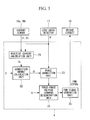
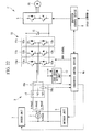
- Fig. 1 is a schematic view illustrating the configuration of a motor driver (load driver) 1 for a compressor motor 20 in an air conditioner according to a first embodiment of the present invention.
- the motor driver 1 includes a converter 3 that converts alternate current (AC) power from a three-phase AC power supply 2 into direct current (DC) power, a converter control device 4 that controls the converter 3, an inverter 5 that converts the DC power output from the converter 3 into three-phase AC power and outputs the three-phase AC power to the compressor motor 20, and an inverter control device 6 that controls the inverter 5.
- AC alternate current
- DC direct current
- inverter 5 that converts the DC power output from the converter 3 into three-phase AC power and outputs the three-phase AC power to the compressor motor 20
- an inverter control device 6 that controls the inverter 5.
- the converter 3 includes a bridge circuit 10 having switch units 11a, 11b, and 11c provided for each of R-phase, S-phase, and T-phase of the three-phase AC power supply 2.
- the switch units 11a, 11b, and 11c include upper arm switching elements 12a, 12b and 12c and lower arm switching elements 13a, 13b and 13c, respectively.
- the upper arm switching elements 12a, 12b and 12c, and the lower arm switching elements 13a, 13b and 13c have junction points each connected to corresponding phases via a reactor 14.
- a smoothing capacitor 15 is connected to between the positive electrode terminals and the negative electrode terminals at the output side of the bridge circuit 10.
- the converter 3 has current sensors 16a and 16b provided for detecting currents of two phases, such as R-phase (first phase) and T-phase (second phase), out of the three phases.
- the converter 3 also has a zero cross detection unit 17 provided for comparing any one phase, such as R-phase, out of the three phases and a neutral point of the three-phase AC power supply 2 to detect a voltage phase ⁇ of the R-phase.
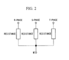
- the zero cross detection unit 17 connects each of the R-phase, the S-phase, and the T-phase via resistances to form a pseudo neutral point N', and compares the pseudo neutral point N' and the R-phase to detect the R-phase voltage phase ⁇ as illustrated in Fig. 2 .
- the converter control device 4 is a micro processing unit (MPU) having a computer-readable recording medium storing a program that implements processing of respective units described below.
- MPU micro processing unit
- the CPU downloads the program stored in the recording medium to a main storage such as a RAM and executes the program, the processing in the respective units as shown below is implemented.
- the computer-readable recording medium include magnetic disks, magneto-optical disks, and semiconductor memory devices, and the like.
- the converter control device 4 is configured to allow two-way communication with the inverter control device 6.
- the inverter 5 includes an upper arm switching element and a lower arm switching element provided for each of the phases.
- these switching elements are driven based on PWM signals generated by the inverter control device 6, the three-phase AC voltage to be supplied to the compressor motor 20 is generated.
- the inverter control device 6 generates the PWM signals of the respective phases which make the speed of the compressor motor 20 coincide with a speed command ⁇ given from a higher order control device (illustration omitted), and gives the PWM signals to the inverter 5.
- Fig. 3 is a functional block diagram of the converter control device 4. As illustrated in Fig. 3 , the converter control device 4 includes a reactive current calculation unit 21, a correction amount calculation unit 22, a phase correction unit 23, a three-phase voltage command determination unit 24, and a PWM generation unit (driving signal generation means) 25 as main components.
- the converter control device 4 includes a reactive current calculation unit 21, a correction amount calculation unit 22, a phase correction unit 23, a three-phase voltage command determination unit 24, and a PWM generation unit (driving signal generation means) 25 as main components.
- the reactive current calculation unit 21 receives input of the R-phase and T-phase current detection values Ir and It measured by the current sensors 16a and 16b, and the R-phase voltage phase ⁇ detected by the zero cross detection unit 17.
- Ir represents an R-phase current detection value
- It represents a T-phase current detection value
- ⁇ represents an R-phase voltage phase detected by the zero cross detection unit 17.
- the reactive current Iq calculated by the reactive current calculation unit 21 is output to the correction amount calculation unit 22.
- the phase correction amount ⁇ may be calculated by proportional plus integral control instead of the integral control.
- a value obtained by, for example, performing the proportional plus integral control on a difference ⁇ Vdc between a target voltage Vdc* that is a preset specified converter voltage (both end voltages of the smoothing capacitor 15) and a measured converter voltage Vdc may be used as the voltage command value k.
- a table in which the voltage command value k and the converter voltage Vdc are associated with each other may be prepared in advance, and the voltage command value k corresponding to the converter voltage Vdc may be set by using this table as illustrated in Fig. 5 .
- the converter voltage Vdc has a tendency to decrease as the load (for example, the speed of a motor, and the like) is higher as illustrated with a curved line "control not performed" in Fig. 6 . Therefore, in consideration of such a tendency, the relation between the voltage command value k and the converter voltage Vdc, which can maintain the converter voltage Vdc at a constant value even with changes in load, may be prepared in advance as a table, and the voltage command value k may be set with use of this table.
- the PWM signal generating unit 25 compares the phase voltage commands V r *, V s *, and V t * of the respective phases determined by the three-phase voltage command determination unit 24 with a triangular wave having a specified carrier frequency so as to generate PWM signals which are switching driving signals of the switch units 11a, 11b, and 11c corresponding to the respective phases.
- the PWM signal generating unit 25 provides the PWM signals to the bridge circuit 10 in the converter 3.
- Fig. 8 illustrates an example of PWM signals of the upper arm switching element and the lower arm switching element in the R-phase when the voltage command value k is 1.
- Fig. 9 illustrates an example of PWM signals of the upper arm switching element and the lower arm switching element in the R-phase when the voltage command value k is 1.5.
- PWM signals of the S-phase and the T-phase are also generated in a similar way.
- a specified time delay Td is provided to on-timing of the upper arm switching element and the lower arm switching element as illustrated in Figs. 10 and 11 .
- Fig. 10 illustrates an example of the PWM signals when an R-phase phase current is positive.
- Fig. 11 illustrates an example of the PWM signals when the R-phase phase current is negative.
- the upper arm switching element and the lower arm switching element are controlled so that one switching element falls and then after a lapse of the time delay Td after the fall, the other switching element rises.
- the time delay Td is a value which can arbitrarily be set in accordance with the characteristics of the switching elements (for example, power transistors and the like).
- a period of time when RN voltage is applied does not coincide with time Pf+Pa determined by the comparison between the phase voltage command V r * and the triangular wave.
- RN voltage application time is Pf+Pa+Td, and therefore the RN voltage is controlled to be larger.
- the RN voltage application time is Pf+Pa-Td, and therefore the RN voltage is controlled to be smaller.
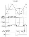
- such an error may be corrected by, for example, correcting the falling timing of the lower arm and the rising timing of the upper arm as illustrated in Figs. 12 and 13 .
- a pulse of the lower arm is made to fall not at time t1 when the phase voltage command V r * and the triangular wave intersect, but at time t2 after a lapse of correction time Tc from the time t1.
- a pulse of the upper arm is made to rise at time t3 after a lapse of the time delay Td from the time t2 when the pulse of the lower arm falls.
- the pulse of the upper arm is made to fall not at time t4 when the phase voltage command V r * and the triangular wave intersect, but at time t5 after a lapse of a specified correction time Tc from the time t4 as illustrated in Fig. 13 .
- the pulse falling timing of the lower arm is corrected to be delayed by the specified correction time Tc.
- the pulse falling timing of the upper arm is corrected to be delayed by the specified correction time Tc.
- the PWM signals generated by the PWM signal generation unit 25 are each given to the switch units 11a, 11b, and 11c corresponding to the respective phases, so that turning on and off of the respective switching elements are controlled.
- a start signal is input from an upper device to the inverter control device 6.
- the inverter control device 6 Upon reception of the start signal, the inverter control device 6 outputs a start signal to the converter control device 4.
- the converter control device 4 sets the value k in accordance with the table illustrated in Fig. 4 and also generates PWM signals corresponding to the respective phases based on the following procedures.
- the current detection values Ir and It and the R-phase voltage phase ⁇ are input to the reactive current calculation unit 21.
- the reactive current Iq is calculated.
- the correction amount calculation unit 22 the correction amount ⁇ of the R-phase voltage phase for zeroing the reactive current Iq is calculated, and this phase correction amount ⁇ is output to the phase correction unit 23.
- the phase voltage commands V r *, V s *, and V t * corresponding to the respective phases are determined by using the voltage command value k set based on the table illustrated in Fig. 4 and the R-phase voltage phase ⁇ ' from the phase correction unit 23. Based on the phase voltage commands V r *, V s *, and V t *, PWM signals for the respective phases are produced by the PWM signal generation unit 25.
- the PWM signals of the respective phases are given to the bridge circuit 10. Based on the PWM signals, on-off control of the upper arm switching elements 12a, 12b and 12c, and the lower arm switching elements 13a, 13b and 13c of the respective switch units 11a, 11b and 11c is performed.
- a voltage between the terminals of the smoothing capacitor 15 gradually rises and once the voltage reaches a specified value, a start end signal is output from the converter control device 4 to the inverter control device 6.
- the inverter control device 6 receives the signal, and starts control on the inverter 5.
- the DC power output from the converter 3 is converted into three-phase AC power and is supplied to the compressor motor 20, by which operation of the compressor motor 20 is started.
- the converter control device 4 After the converter 3 is started, the converter control device 4 repeatedly performs a series of the above-stated processing including setting the voltage command value k, calculating the phase correction amount ⁇ , and correcting the voltage phase ⁇ in accordance with a specified algorithm. Accordingly, the PWM signals are generated in a specified period, and the bridge circuit 10 is controlled so that the converter voltage becomes constant.
- the reactive current Iq is calculated based on the R-phase and T-phase current detection values Ir and It and the information on the R-phase voltage phase ⁇ , the R-phase voltage phase difference that zeros the reactive current Iq is calculated as a phase correction amount ⁇ , and the phase voltage commands of the respective phases are determined by using the voltage phase ⁇ ' obtained by correcting the R-phase voltage phase ⁇ with the phase correction amount ⁇ .
- a phase difference between the power supply voltage and the power supply current can be zeroed. This makes it possible to keep the power factor to 1, without influence of the size of the load.
- the reactive current is detected in the reactive current calculation unit 21 by using the voltage phase ⁇ from the zero cross detection unit 17.
- the reactive current may be calculated through an arithmetic calculation of the voltage phase ⁇ by using the following expression (7).
- ⁇ 2 ⁇ ⁇ fT
- f is power supply frequency and T is time.
- the power supply frequency a value may be registered in advance, or the power supply frequency may sequentially be detected, and the detected value may be substituted.
- the above-stated method may be replaced by a method in which a previous value of the corrected phase ⁇ ' determined by the phase correction unit 23 is used as the voltage phase ⁇ .
- the S-phase or T-phase voltage phase may be corrected instead of the R-phase voltage phase.
- the R-phase and T-phase currents are detected by the current sensors 16a and 16b, the currents of any two phases may be detected, and a combination thereof may arbitrarily be set.
- the phase of the voltage phase ⁇ detected by the zero cross detection unit 17 is not limited to the R-phase, but may be the S-phase and the T-phase.
- the respective phase voltage commands V r *, V s *, and V t * of the R-phase, S-phase, and T-phase are determined by using the above expressions (4) to (6).
- the respective phase voltage commands V r *, V s *, and V t * of the R-phase, S-phase, and the T-phase may be determined by using the detected phases of the respective phases according to the following expressions (8) to (10).
- V r * ksin ⁇ r - ⁇
- V s * ksin ⁇ s - ⁇
- V t * ksin ⁇ t - ⁇
- ⁇ r is a detected phase of the R-phase
- ⁇ s is a detected phase of the S-phase
- ⁇ t is a detected phase of the T-phase.
- ⁇ is a phase correction amount.
- a step-down circuit 30 which is connected to an auxiliary machine may be connected to both ends of the smoothing capacitor 15 of the converter 3, so that the DC power generated by the converter 3 is stepped down to a specified voltage value by the step-down circuit 30, and the stepped-down DC power may be supplied to the auxiliary machine 31.
- a 400V-class motor is generally used as the compressor motor 20
- a 200V-class motor is used as the auxiliary machine 31 such as a fan motor. Accordingly, when the converter voltage generated by the converter 3 is stepped down by the step-down circuit 30 and then is supplied to the auxiliary machine 31, it becomes possible to use the auxiliary machine whose effect of suppressing the higher harmonic of the input current is enhanced as compared with the case where the phase voltage of the power supply is rectified and then is connected to the auxiliary machine 31.
- Fig. 15 illustrates the functional block diagram of a converter control device 4' according to the present embodiment. As illustrated in Fig. 15 , the converter control device 4' according to the present embodiment is different from the converter control device 4 according to the above-disclosed first embodiment in the point of further including an unbalance correction processing unit 26.
- a large difference may be generated between the respective phase voltages as compared with the time when voltages are balanced.
- the compressor motor 20 in the voltage balanced state where an R-S interphase voltage is 415V, a T-S interphase voltage is 415V, and an R-T interphase voltage is 415V, the compressor motor 20 has a speed of 120rps and a torque of 6.7 Nm as a load.
- R-phase, S-phase and T-phase current waveforms are substantially identical as illustrated in Fig. 16 .
- the switching unit 11c is operated in an attempt to step up the voltage and to charge the smoothing capacitor 15.
- the step-up voltage is small, it can hardly charge the smoothing capacitor 15.
- the T-phase current is considered to become smaller and end up forming the current waveform as illustrated in Fig. 17 .
- the peak values of the R-phase and S-phase current waves are also different from each other. However, this is considered to be attributed to error of the PWM signals and/or variations in characteristics of the switching elements. Ideally, the same-size currents are considered to flow.
- the present embodiment is characterized by the unbalance correction processing unit 26 provided for suppressing variations in the current values of the respective phases when such voltage unbalance occurs.
- the unbalance correction processing unit 26 determines that the three-phase AC power supply 2 is in the voltage unbalanced state, corrects amplitude values of the phase voltage commands V r *, V s *, and V t * determined by the three-phase voltage command determination unit 24 with use of the size relation between the current values of the respective phases, and outputs corrected phase voltage commands V r *', V s *', and V t *' to the PWM generation unit 25.
- a preset specified threshold value for example, 0.5A
- the unbalance correction processing unit 26 gradually increase the amplitude value of the phase voltage command corresponding to the phase that indicates a maximum current value or gradually decreases the amplitude value of the phase voltage command corresponding to the phase that indicates a minimum current value until the respective phase currents Is, Ir and It substantially coincide.
- ⁇ r , ⁇ s , and ⁇ t are correction coefficients and their initial values are set to 1.
- the correction coefficients have an upper limit preset to 1 and a lower limit preset to a specified value. The correction coefficients are adjusted within the range of these upper and lower limits.
- the amplitude values of the phase voltage commands V r *, V s *, and V t * determined by the three-phase voltage command determination unit 24 are corrected by adjusting the correction coefficients ⁇ r , ⁇ s , and ⁇ t in accordance with the size relation between the current values of the respective phases.
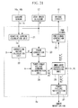
- the unbalance correction processing unit 26 repeatedly executes the following processing in a specified period.
- the unbalance correction processing unit 26 acquires R-phase and T-phase current detection values Ir and It measured by the current sensors 16a and 16b (step SA1), and calculates an estimated current value Is of the S-phase through an arithmetic calculation using the current detection values Ir and It of these two phases (step SA2).
- step SA3 among the current values of three phases, a maximum current value and a minimum current value are identified, and a difference between the maximum current value and the minimum current value is calculated (step SA3).
- it is determined whether or not the difference is equal to or more than a preset specified threshold value (step SA4). If the difference is less than the threshold value, it is determined that the power supply 2 is not in the voltage unbalanced state, and this processing is ended ("NO" in step SA4).
- step SA4 it is determined whether or not the correction coefficient ⁇ a corresponding to the maximum current phase (the phase that indicates the maximum current value) is 1, i.e., whether or not the correction coefficient ⁇ is set to the maximum value (step SA5).
- the maximum current phase is the S-phase
- step SA5 If the correction coefficient ⁇ corresponding to the maximum current phase is not 1 ("NO” in step SA5) as a result of determination, then the correction coefficient ⁇ corresponding to the maximum current phase is increased by a specified amount (step SA6), and this processing is ended. If the correction coefficient corresponding to the maximum current phase is 1 (upper limit) ("YES" in step SA5), the correction coefficient corresponding to the minimum current phase is decreased by a specified amount (step SA7), and this processing is ended.
- the following voltage control is performed by repeated execution of the above processing.
- the T-phase power supply voltage increases.
- the T-phase current becomes larger than other S-phase and R-phase currents this time.
- the correction coefficients ⁇ r , ⁇ s , and ⁇ t of the respective phases are gradually increased or decreased in accordance with the size relation of the phase currents so as to control the step-up voltages of the respective phases. As a result, it becomes possible to make the current values of the respective phases substantially coincide.
- Fig. 19 illustrates current waveforms of the respective phases when voltage unbalance occurs.
- Fig. 20 illustrates current waveforms of the respective phases after unbalance correction processing is performed in the voltage unbalanced state illustrated in Fig. 19 .
- executing the unbalance correction as described in the foregoing can make the currents of the respective phases substantially coincide.
- the unbalance correction processing unit 26 may determine whether or not an average of the currents of the respective phases is equal to or more than a preset specified value. If the average is equal to or more than the specified value, the above-described correction of the phase voltage commands may be performed. When the phase voltage commands are corrected in this way in a load region where the average of the respective phase currents is equal to or more than a specified value, it becomes possible to perform stable voltage step-up control.
- a converter control device 4a according to a third embodiment of the present invention is described with reference to Fig. 21 .
- a converter control device 4a according to the present embodiment is configured by further providing the converter control device 4' according to the above-disclosed second embodiment with a power failure notification unit 27.
- the power failure notification unit 27 determines occurrence of power failure, and performs error notification.
- the error notification is performed by displaying an error on a display unit not illustrated, or by emitting a sound.
- shutdown of the converter 3 may be performed, and shutdown of the motor driver 1 may further be performed.
- Providing such a power failure notification unit 27 enables the motor driver 1 to estimate the voltage unbalanced state which is not assumed on the power supply system side.
- an air conditioner 1' as illustrated in Fig. 22 may also be embodied, for example.
- the air conditioner 1' has an indoor unit (for example, a control device, a fan motor, and the like of an indoor unit in particular) 7 connected to a power line of any one phase (for example, R-phase) out of power lines of three phases connected to the three-phase AC power supply 2, and an outdoor unit (for example, a control device, a fan motor, and the like of an outdoor unit in particular) 8 connected to a power line of one phase (for example, S-phase), out of the power lines of three phases connected to the three-phase AC power supply 2, other than the phase connected to the indoor unit 7.
- an indoor unit for example, a control device, a fan motor, and the like of an indoor unit in particular
- the power failure notification unit 27 of the converter control device 4a determines occurrence of power failure and performs the above-stated error notification. In addition, the power failure notification unit 27 identifies a phase corresponding to the voltage command value that satisfies the above conditions, and notifies the error to the connected indoor unit 7 or the outdoor unit 8 connected to the aforementioned phase.
- an error notification threshold value based on voltage design values allowable in the indoor unit 7 and the outdoor unit 8. For example, when the voltage value of the supply voltage becomes below the voltage value allowable in the indoor unit 7 and/or the outdoor unit 8, the error notification may be performed. Detecting the voltage unbalanced state and performing error notification in this way enable the indoor unit 7 and the outdoor unit 8 to ascertain that the error is occurring due to the voltage unbalance or due to other causes.
- the power failure notification unit 27 may store a protecting level threshold value set smaller than the error notification threshold value.
- the power failure notification unit 27 may output a shutdown signal to the indoor unit 7 or the outdoor unit 8 connected to the corresponding phase. Thus, outputting a shutdown signal enables the indoor unit 7 and the outdoor unit 8 to be protected.
Landscapes
- Engineering & Computer Science (AREA)
- Power Engineering (AREA)
- Inverter Devices (AREA)
- Rectifiers (AREA)
- Control Of Ac Motors In General (AREA)
- Air Conditioning Control Device (AREA)
Abstract
Description
- The present invention relates to a converter control device, method, and program, and an air conditioner.
- As a converter device which converts three-phase alternating current (AC) voltage output from a three-phase AC power supply into direct current (DC) voltage, a PWM rectifier disclosed in
PTL 1 has conventionally been known. - {PTL 1} Japanese Unexamined Patent Application, Publication No.
Hei 10-164845 - According to the PWM rectifier disclosed in
PTL 1, the power factor can be controlled to about 1 in a certain load where a control parameter is set, whereas the power factor cannot be controlled to 1 in other load regions. - An object of the present invention is to provide a converter control device, method, and program, and an air conditioner capable of controlling the power factor to about 1 irrespective of a load.
- A first aspect of the present invention is a converter control device used for a converter, the converter including a bridge circuit for converting three-phase AC voltage output from a three-phase AC power supply into DC voltage and outputting the DC voltage, the bridge circuit having a pair of switch units provided for each phase of the three-phase AC power supply, the pair of switch units including an upper arm switching element and a lower arm switching element, the upper arm switching element and the lower arm switching element having a junction point connected to each corresponding phase, the converter control device including: a reactive current calculation means that calculates a reactive current by using current detection values of any two phases and a voltage phase of any one phase; a correction amount calculation means that calculates a phase difference between the voltage phase of the phase and a voltage phase of the phase for zeroing the reactive current; a phase correction means that corrects the voltage phase of the phase by using the phase difference calculated by the correction amount calculation means; a three-phase voltage command determination means that determines phase voltage commands corresponding to the respective phases based on a predetermined voltage command value and a corrected voltage phase of the phase; and a driving signal generation means that generates driving signals for the switch units corresponding to the respective phases by using the phase voltage commands.
- According to the present aspect, a reactive current is calculated based on current detection values of any two phases and a voltage phase of any one phase, a voltage phase difference for zeroing the reactive current zero is calculated, and phase voltage commands of the respective phases are determined by using a voltage phase corrected with the phase difference with which the voltage phase of the phase was calculated. As a result, it becomes possible to zero the phase difference between the power supply voltage and the power supply current. This makes it possible to keep the power factor to 1, without influence of the size of the load.
- In the converter control device, the voltage phase of the phase used in the reactive current calculation means may be a value detected by a zero cross detection means, or a previous value of the corrected voltage phase of the phase calculated by the phase correction means, or may be calculated through an arithmetic calculation using a phase formula including power supply frequency and time as a parameter.
- The converter control device may also include a zero cross detection means connected to the one phase and to a neutral point of the power supply, the zero cross detection means detecting the voltage phase of the phase. When the three-phase AC power supply does not have a neutral point, a pseudo neutral point formed by connecting the respective phases via resistances may be used in place of the neutral point of the three-phase AC power supply.
- In the converter control device, when a specified time delay is set for on-and-off timing of switching the upper arm switching element and the lower arm switching element in an identical phase to prevent the switching elements from being simultaneously turned on, the driving signal generation means may generate PWM signals wherein the off-timing of the lower arm switching element corresponding to the phase is delayed by a specified correction time if current of the phase is positive and the off-timing of the upper arm switching element corresponding to the phase is delayed by the specified correction time if the current of the phase is negative.
- By generating such PWM signals, an inconvenience associated with providing the specified time delay can be reduced, and this makes it possible to enhance a higher harmonic suppressing effect.
- The converter control device may include an unbalance correction processing means, wherein when the difference between the current values of any two phases out of current values of the respective phases reaches a preset specified threshold value or more, the unbalance correction processing means may determine that the three-phase AC power supply is in a voltage unbalanced state, may correct amplitude values of the phase voltage commands determined by the three-phase voltage command determination means with use of a size relation of the current values of the respective phases, and may output the corrected phase voltage commands to the driving signal generation means.
- According to such a configuration, when it is determined that the power supply is in the voltage unbalanced state, the amplitude values of the phase voltage commands determined by the three-phase voltage command determination means are corrected in accordance with the size relation of the phase currents. As a result, step-up voltages of the respective phases can be adjusted in accordance with the current values. Accordingly, even when the voltage unbalance occurs, it becomes possible to set the current values of the respective phases to be a substantially identical value.
- In the converter control device, when the three-phase AC power supply is determined to be in the voltage unbalanced state, the unbalance correction processing means may gradually increases an amplitude value of the phase voltage command corresponding to a phase that indicates a maximum current value or may gradually decrease an amplitude value of the phase voltage command corresponding to a phase that indicates a minimum current value until the respective phase currents coincide.
- Thus, when it is determined that the three-phase AC power supply is in the unbalance state, the amplitude value of the phase voltage command corresponding to the phase that indicates the maximum current value is gradually increased or the amplitude value of the phase voltage command corresponding to the phase that indicates the minimum current value is gradually decreased until the respective phase currents coincide. This makes it possible to make the current values of the respective phases efficiently and easily coincide. An upper limit and a lower limit of the amplitude value are set in advance, and the amplitude value is limited within the range of these upper and lower limit values.
- In the converter control device, the amplitude values of the phase voltage commands may be corrected by the unbalance correction processing means when an average of the respective phase currents is a preset specified value or more.
- Thus, the phase voltage commands are corrected in an operating state of a load where the average of the respective phase currents becomes a specified value or more. As a result, it becomes possible to perform stable step-up control.
- A second aspect of the present invention is a load driver, including: a converter including a bridge circuit for converting three-phase AC voltage output from a three-phase AC power supply into DC voltage and outputting the DC voltage, the bridge circuit having a pair of switch units provided for each phase of the three-phase AC power supply, the pair of switch units including an upper arm switching element and a lower arm switching element, the upper arm switching element and the lower arm switching element having a junction point connected to each corresponding phase; a converter control means that controls the converter; an inverter that converts the DC voltage output from the converter into three-phase AC voltage and supplies the three-phase AC voltage to a load; and an inverter control means that controls the inverter, wherein the converter control means includes: a reactive current calculation means that calculates a reactive current by using current detection values of any two phases and a voltage phase of any one phase; a correction amount calculation means that calculates a phase difference between the voltage phase of the phase and a voltage phase of the phase for zeroing the reactive current; a phase correction means that corrects the voltage phase of the phase by using the phase difference calculated by the correction amount calculation means; a three-phase voltage command determination means that determines phase voltage commands corresponding to the respective phases based on a predetermined voltage command value and a corrected voltage phase of the phase; and a driving signal generation means that generates driving signals for the switch units corresponding to the respective phases by using the phase voltage commands.
- A third aspect of the present invention is an air conditioner including the load driver.
- Such an air conditioner may include a step-down means that branches DC power input from the converter to the inverter to step down voltage of the DC power, wherein output power of the step-down means may be supplied to an air conditioning auxiliary machine.
- A fourth aspect of the present invention is an air conditioner, including: a converter including a bridge circuit for converting three-phase AC voltage output from a three-phase AC power supply into DC voltage and outputting the DC voltage, the bridge circuit having a pair of switch units provided for each phase of the three-phase AC power supply, the pair of switch units including an upper arm switching element and a lower arm switching element, the upper arm switching element and the lower arm switching element having a junction point connected to each corresponding phase; a converter control device according to any one of the aspects; an inverter that converts the DC voltage output from the converter into three-phase AC voltage and supplies the three-phase AC voltage to a compressor motor; an inverter control means that controls the inverter; an indoor unit connected to a power line of any one phase out of power lines of three phases connected to the three-phase AC power supply; an outdoor unit connected to a power line of one phase, out of the power lines of three phases connected to the three-phase AC power supply, other than the power line of the phase connected to the indoor unit, wherein the converter control means includes a power failure notification means that performs error notification notifying power failure when the corrected phase voltage commands output from the unbalance correction processing means include a phase voltage command whose peak value is equal to or less than a preset specified error notification threshold value, the power failure being notified to the indoor unit or the outdoor unit connected to a corresponding phase.
- According to the aforementioned aspect, the error attributed to the voltage unbalanced state can be notified to the indoor unit and the outdoor unit which receive electric power from the three-phase AC power supply. Accordingly, the indoor unit and outdoor unit side can ascertain the cause of an abnormality which is currently occurring.
- In the air conditioner, when the corrected phase voltage commands output from the unbalance correction processing means include a phase voltage command whose peak value is equal to or less than a protection level threshold value set smaller than the error notification threshold value, the power failure notification means may output a signal instructing shutdown to the indoor unit or the outdoor unit connected to a corresponding phase.
- Thus, outputting a shutdown signal enables the indoor unit and the outdoor unit to be protected.
- A fifth aspect of the present invention is a method for converter control used for a converter, the converter including a bridge circuit for converting three-phase AC voltage output from a three-phase AC power supply into DC voltage and outputting the DC voltage, the bridge circuit having a pair of switch units provided for each phase of the three-phase AC power supply, the pair of switch units including an upper arm switching element and a lower arm switching element, the upper arm switching element and the lower arm switching element having a junction point connected to each corresponding phase, the method for converter control including: a reactive current calculating step of calculating a reactive current by using current detection values of any two phases and a voltage phase of any one phase; a correction amount calculation step of calculating a phase difference between the voltage phase of the phase and a voltage phase of the phase for zeroing the reactive current; a phase correction step of correcting the voltage phase of the phase by using the phase difference; a three-phase voltage command determination step of determining phase voltage commands corresponding to the respective phases based on a predetermined voltage command value and a corrected voltage phase of the phase; and a driving signal generation step of generating driving signals for the switch units corresponding to the respective phases by using the phase voltage commands.
- A sixth aspect of the present invention is a converter control program used for a converter, the converter including a bridge circuit for converting three-phase AC voltage output from a three-phase AC power supply into DC voltage and outputting the DC voltage, the bridge circuit having a pair of switch units provided for each phase of the three-phase AC power supply, the pair of switch units including an upper arm switching element and a lower arm switching element, the upper arm switching element and the lower arm switching element having a junction point connected to each corresponding phase, the converter control program causing a computer to execute: a reactive current calculation process of calculating a reactive current by using current detection values of any two phases and a voltage phase of any one phase; a correction amount calculation process of calculating a phase difference between the voltage phase of the phase and a voltage phase of the phase for zeroing the reactive current; a phase correction process of correcting the voltage phase of the phase by using the phase difference; a three-phase voltage command determination process of determining phase voltage commands corresponding to the respective phases based on a predetermined voltage command value and a corrected voltage phase of the phase; and a driving signal generation process of generating driving signals for the switch units corresponding to the respective phases by using the phase voltage commands.
- According to the present invention, an effect of being able to control the power factor to about 1 irrespective of a load is implemented.
-
- {
Fig. 1} Fig. 1 is a schematic view illustrating the configuration of a drive control device for a compressor motor in an air conditioner according to a first embodiment of the present invention. - {
Fig. 2} Fig. 2 is an explanatory view of a pseudo neutral point. - {
Fig. 3} Fig. 3 is a functional block diagram of a converter control device according to the first embodiment of the present invention. - {
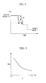
Fig. 4} Fig. 4 illustrates a setting example of a voltage command value at the time of startup. - {
Fig. 5} Fig. 5 illustrates an example of a table indicating relation between a voltage command value and a converter voltage. - {
Fig. 6} Fig. 6 illustrates relation between a load and a converter voltage when the voltage command value is set by using the table illustrated inFig. 5 . - {
Fig. 7} Fig. 7 illustrates relation between a power supply voltage and a converter voltage when the voltage command value is set by using the table illustrated inFig. 5 . - {
Fig. 8} Fig. 8 illustrates an example of PWM signals of an upper arm switching element and a lower arm switching element in R-phase when the voltage command value is 1. - {
Fig. 9} Fig. 9 illustrates an example of PWM signals of the upper arm switching element and the lower arm switching element in the R-phase when the voltage command value is 1.5. - {
Fig. 10} Fig. 10 illustrates an example of a method for generating the PWM signal. - {
Fig. 11} Fig. 11 illustrates an example of the method for generating the PWM signal. - {
Fig. 12} Fig. 12 illustrates another example of the method for generating the PWM signal. - {
Fig. 13} Fig. 13 illustrates another example of the method for generating the PWM signal. - {
Fig. 14} Fig. 14 illustrates one configuration example in the case of supplying converter voltage to an auxiliary machine. - {
Fig. 15} Fig. 15 is a functional block diagram of a converter control device according to a second embodiment of the present invention. - {
Fig. 16} Fig. 16 illustrates an example of current waveforms of respective phases in a balanced voltage state. - {
Fig. 17} Fig. 17 illustrates an example of the current waveforms of the respective phases in a voltage unbalanced state. - {
Fig. 18} Fig. 18 is a flow chart illustrating procedures of processing executed by an unbalance correction processing unit illustrated inFig. 15 . - {
Fig. 19} Fig. 19 illustrates an example of current waveforms of respective phases in the voltage unbalanced state. - {
Fig. 20} Fig. 20 illustrates current waveforms of the respective phases after performing unbalance correction processing in the voltage unbalanced state illustrated inFig. 19 . - {
Fig. 21} Fig. 21 is a functional block diagram of a converter control device according to a third embodiment of the present invention. - {
Fig. 22} Fig. 22 illustrates one aspect of an air conditioner including the converter control device illustrated inFig. 20 . - Hereinbelow, embodiments of the converter control device, method and program according to the present invention in the case of being applied to an air conditioner will be described with reference to the drawings.
-
Fig. 1 is a schematic view illustrating the configuration of a motor driver (load driver) 1 for acompressor motor 20 in an air conditioner according to a first embodiment of the present invention. As illustrated inFig. 1 , themotor driver 1 includes aconverter 3 that converts alternate current (AC) power from a three-phaseAC power supply 2 into direct current (DC) power, aconverter control device 4 that controls theconverter 3, aninverter 5 that converts the DC power output from theconverter 3 into three-phase AC power and outputs the three-phase AC power to thecompressor motor 20, and aninverter control device 6 that controls theinverter 5. - The
converter 3 includes abridge circuit 10 havingswitch units AC power supply 2. Theswitch units arm switching elements arm switching elements respective switch unit arm switching elements arm switching elements reactor 14. A smoothingcapacitor 15 is connected to between the positive electrode terminals and the negative electrode terminals at the output side of thebridge circuit 10. - The
converter 3 hascurrent sensors converter 3 also has a zerocross detection unit 17 provided for comparing any one phase, such as R-phase, out of the three phases and a neutral point of the three-phaseAC power supply 2 to detect a voltage phase θ of the R-phase. When the three-phase AC power supply does not have a neutral point, the zerocross detection unit 17 connects each of the R-phase, the S-phase, and the T-phase via resistances to form a pseudo neutral point N', and compares the pseudo neutral point N' and the R-phase to detect the R-phase voltage phase θ as illustrated inFig. 2 . - Current detection values Ir and It of the R-phase and the T-phase measured by the
current sensors cross detection unit 17 are output to theconverter control device 4. - For example, the
converter control device 4 is a micro processing unit (MPU) having a computer-readable recording medium storing a program that implements processing of respective units described below. When the CPU downloads the program stored in the recording medium to a main storage such as a RAM and executes the program, the processing in the respective units as shown below is implemented. Examples of the computer-readable recording medium include magnetic disks, magneto-optical disks, and semiconductor memory devices, and the like. - The
converter control device 4 is configured to allow two-way communication with theinverter control device 6. - As in the case of the
converter 3, theinverter 5 includes an upper arm switching element and a lower arm switching element provided for each of the phases. When these switching elements are driven based on PWM signals generated by theinverter control device 6, the three-phase AC voltage to be supplied to thecompressor motor 20 is generated. - The
inverter control device 6 generates the PWM signals of the respective phases which make the speed of thecompressor motor 20 coincide with a speed command ω given from a higher order control device (illustration omitted), and gives the PWM signals to theinverter 5. - Now, the
converter control device 4 is described with reference toFig. 3 . -
Fig. 3 is a functional block diagram of theconverter control device 4. As illustrated inFig. 3 , theconverter control device 4 includes a reactivecurrent calculation unit 21, a correctionamount calculation unit 22, aphase correction unit 23, a three-phase voltagecommand determination unit 24, and a PWM generation unit (driving signal generation means) 25 as main components. - The reactive
current calculation unit 21 receives input of the R-phase and T-phase current detection values Ir and It measured by thecurrent sensors cross detection unit 17. - The reactive
current calculation unit 21 calculates a reactive current Iq by these input information pieces and an expression (1) shown below:
- In the expression (1), Ir represents an R-phase current detection value, It represents a T-phase current detection value, and θ represents an R-phase voltage phase detected by the zero
cross detection unit 17. The reactive current Iq calculated by the reactivecurrent calculation unit 21 is output to the correctionamount calculation unit 22. - The correction
amount calculation unit 22 calculates a voltage phase difference of the R-phase which zeros the reactive current Iq, as a phase correction amount Φ. Specifically, the correctionamount calculation unit 22 performs integral control to calculate the phase correction amount Φ which zeros the reactive current Iq. For example, the phase correction amount Φ is calculated by the following expression (2):
- The phase correction amount Φ may be calculated by proportional plus integral control instead of the integral control.
- The
phase correction unit 23 corrects the R-phase voltage phase θ detected by the zerocross detection unit 17 with use of the phase correction amount Φ calculated by the correctionamount calculation unit 22 to obtain a corrected phase θ'. Specifically, thephase correction unit 23 corrects the voltage phase θ by subtracting the phase correction amount Φ from the R-phase voltage phase θ input from the zerocross detection unit 17 as expressed by the expressions (3) shown below:
- The three-phase voltage
command determination unit 24 determines phase voltage commands corresponding to the respective phases by using a predetermined voltage command value k and the corrected voltage phase θ' input from thephase correction unit 23. Specifically, respective phase voltage commands Vr*, Vs*, and Vt* of the R-phase, the S-phase, and the T-phase are determined respectively based on the following expressions (4) to (6):


- Here, as illustrated in
Fig. 4 for example, the voltage command value k is set to k= 1.5 at the time of startup of theconverter 3. The voltage command value k is changed so as to be decreased to k= 1.0 in stages over time. - After the
converter 3 is started, a value obtained by, for example, performing the proportional plus integral control on a difference ΔVdc between a target voltage Vdc* that is a preset specified converter voltage (both end voltages of the smoothing capacitor 15) and a measured converter voltage Vdc may be used as the voltage command value k. - Instead of this, a table in which the voltage command value k and the converter voltage Vdc are associated with each other may be prepared in advance, and the voltage command value k corresponding to the converter voltage Vdc may be set by using this table as illustrated in
Fig. 5 . - For example, the converter voltage Vdc has a tendency to decrease as the load (for example, the speed of a motor, and the like) is higher as illustrated with a curved line "control not performed" in
Fig. 6 . Therefore, in consideration of such a tendency, the relation between the voltage command value k and the converter voltage Vdc, which can maintain the converter voltage Vdc at a constant value even with changes in load, may be prepared in advance as a table, and the voltage command value k may be set with use of this table. - This makes it possible to maintain the converter voltage Vdc constant even when the load changes as illustrated with a line "control performed" in
Fig. 6 for example. As illustrated inFig. 7 , even when the power supply voltage changes to 380V, 400V, and 415V, it becomes possible to control the converter voltage Vdc to be constant and to thereby commonalize the power supply voltage. - The PWM
signal generating unit 25 compares the phase voltage commands Vr*, Vs*, and Vt* of the respective phases determined by the three-phase voltagecommand determination unit 24 with a triangular wave having a specified carrier frequency so as to generate PWM signals which are switching driving signals of theswitch units signal generating unit 25 provides the PWM signals to thebridge circuit 10 in theconverter 3. -
Fig. 8 illustrates an example of PWM signals of the upper arm switching element and the lower arm switching element in the R-phase when the voltage command value k is 1.Fig. 9 illustrates an example of PWM signals of the upper arm switching element and the lower arm switching element in the R-phase when the voltage command value k is 1.5. PWM signals of the S-phase and the T-phase are also generated in a similar way. - Here, when the PWM signals are generated, a specified time delay Td is provided to on-timing of the upper arm switching element and the lower arm switching element as illustrated in
Figs. 10 and11 .Fig. 10 illustrates an example of the PWM signals when an R-phase phase current is positive.Fig. 11 illustrates an example of the PWM signals when the R-phase phase current is negative. - In
Figs. 10 and11 , the upper arm switching element and the lower arm switching element are controlled so that one switching element falls and then after a lapse of the time delay Td after the fall, the other switching element rises. The time delay Td is a value which can arbitrarily be set in accordance with the characteristics of the switching elements (for example, power transistors and the like). - Since the specified time delay Td is given in this way to prevent the upper arm switching element and the lower arm switching element from being simultaneously turned on, short circuit can be prevented.
- According to the method for PWM signal generation illustrated in
Figs. 10 and11 , a period of time when RN voltage is applied does not coincide with time Pf+Pa determined by the comparison between the phase voltage command Vr* and the triangular wave. For example, when the R-phase current illustrated inFig. 10 is positive, RN voltage application time is Pf+Pa+Td, and therefore the RN voltage is controlled to be larger. When the R-phase current illustrated inFig. 11 is negative, the RN voltage application time is Pf+Pa-Td, and therefore the RN voltage is controlled to be smaller. - Accordingly, such an error may be corrected by, for example, correcting the falling timing of the lower arm and the rising timing of the upper arm as illustrated in
Figs. 12 and13 . - For example, as illustrated in
Fig. 12 , when the R-phase current is positive, a pulse of the lower arm is made to fall not at time t1 when the phase voltage command Vr* and the triangular wave intersect, but at time t2 after a lapse of correction time Tc from the time t1. A pulse of the upper arm is made to rise at time t3 after a lapse of the time delay Td from the time t2 when the pulse of the lower arm falls. - Since the pulse falling timing of the lower arm is delayed by the correction time Tc in this way, the RN voltage application time (= Pf+Pa+Td-Tc) can be approximated to the time (= Pf+Pa) obtained by the comparison between the phase voltage command Vr* and the triangular wave as illustrated in
Fig. 12 . Furthermore, setting Tc=Td can make the time obtained by the comparison between the phase voltage command Vr* and the triangular wave coincide with the RN voltage application time. - Similarly, when the R-phase current is negative, the pulse of the upper arm is made to fall not at time t4 when the phase voltage command Vr* and the triangular wave intersect, but at time t5 after a lapse of a specified correction time Tc from the time t4 as illustrated in
Fig. 13 . - The pulse of the lower arm is made to rise at time t6 after a lapse of the time delay Td from the time t5 when the pulse of the upper arm falls. Since the pulse falling timing of the upper arm is delayed by the correction time Tc in this way, the RN voltage application time (= Pf+Pa-Td+Tc) can be approximated to the time (= Pf+Pa) obtained by the comparison between the phase voltage command Vr* and the triangular wave as illustrated in
Fig. 13 . Setting Tc=Td can make the time obtained by the comparison between the phase voltage command Vr* and the triangular wave coincide with the RN voltage application time. - As described in the foregoing, when the phase current is positive, the pulse falling timing of the lower arm is corrected to be delayed by the specified correction time Tc. When the phase current is negative, the pulse falling timing of the upper arm is corrected to be delayed by the specified correction time Tc. As a result, it becomes possible to enhance the higher harmonic suppressing effect.
- The PWM signals generated by the PWM
signal generation unit 25 are each given to theswitch units - A description is now given of a function of the
motor driver 1 according to the present embodiment. - First, at the time of startup of the
motor driver 1, a start signal is input from an upper device to theinverter control device 6. Upon reception of the start signal, theinverter control device 6 outputs a start signal to theconverter control device 4. Upon reception of the start signal, theconverter control device 4 sets the value k in accordance with the table illustrated inFig. 4 and also generates PWM signals corresponding to the respective phases based on the following procedures. - While R-phase and T-phase currents are detected by the
current sensors cross detection unit 17. These detection values are output to theconverter control device 4. - The current detection values Ir and It and the R-phase voltage phase θ are input to the reactive
current calculation unit 21. By using these information pieces and the above-stated expressions (1), the reactive current Iq is calculated. In the correctionamount calculation unit 22, the correction amount Φ of the R-phase voltage phase for zeroing the reactive current Iq is calculated, and this phase correction amount Φ is output to thephase correction unit 23. In thephase correction unit 23, the R-phase voltage phase θ detected by the zerocross detection unit 17 is corrected with the phase correction amount Φ from the correctionamount calculation unit 22, and a corrected R-phase voltage phase θ' (= θ-Φ) is output to the three-phase voltagecommand determination unit 24. - In the three-phase voltage
command determination unit 24, the phase voltage commands Vr*, Vs*, and Vt* corresponding to the respective phases are determined by using the voltage command value k set based on the table illustrated inFig. 4 and the R-phase voltage phase θ' from thephase correction unit 23. Based on the phase voltage commands Vr*, Vs*, and Vt*, PWM signals for the respective phases are produced by the PWMsignal generation unit 25. - The PWM signals of the respective phases are given to the
bridge circuit 10. Based on the PWM signals, on-off control of the upperarm switching elements arm switching elements respective switch units - Accordingly, a voltage between the terminals of the smoothing
capacitor 15 gradually rises and once the voltage reaches a specified value, a start end signal is output from theconverter control device 4 to theinverter control device 6. Theinverter control device 6 receives the signal, and starts control on theinverter 5. As a consequence, the DC power output from theconverter 3 is converted into three-phase AC power and is supplied to thecompressor motor 20, by which operation of thecompressor motor 20 is started. - After the
converter 3 is started, theconverter control device 4 repeatedly performs a series of the above-stated processing including setting the voltage command value k, calculating the phase correction amount Φ, and correcting the voltage phase θ in accordance with a specified algorithm. Accordingly, the PWM signals are generated in a specified period, and thebridge circuit 10 is controlled so that the converter voltage becomes constant. - As described in the foregoing, according to the converter control device, method, and program, and the air conditioner according to the present embodiment, the reactive current Iq is calculated based on the R-phase and T-phase current detection values Ir and It and the information on the R-phase voltage phase θ, the R-phase voltage phase difference that zeros the reactive current Iq is calculated as a phase correction amount Φ, and the phase voltage commands of the respective phases are determined by using the voltage phase θ' obtained by correcting the R-phase voltage phase θ with the phase correction amount Φ. As a result, a phase difference between the power supply voltage and the power supply current can be zeroed. This makes it possible to keep the power factor to 1, without influence of the size of the load.
- In the present embodiment, the reactive current is detected in the reactive
current calculation unit 21 by using the voltage phase θ from the zerocross detection unit 17. Instead of this, the reactive current may be calculated through an arithmetic calculation of the voltage phase θ by using the following expression (7).
- In the above expression (7), f is power supply frequency and T is time. As the power supply frequency, a value may be registered in advance, or the power supply frequency may sequentially be detected, and the detected value may be substituted.
- For example, the above-stated method may be replaced by a method in which a previous value of the corrected phase θ' determined by the
phase correction unit 23 is used as the voltage phase θ. - Although the case of correcting the R-phase voltage phase has been described in the present embodiment, the S-phase or T-phase voltage phase may be corrected instead of the R-phase voltage phase. Although the R-phase and T-phase currents are detected by the
current sensors cross detection unit 17 is not limited to the R-phase, but may be the S-phase and the T-phase. - In the present embodiment, the respective phase voltage commands Vr*, Vs*, and Vt* of the R-phase, S-phase, and T-phase are determined by using the above expressions (4) to (6). In the case where, for example, the phases of the respective phases are detected instead, the respective phase voltage commands Vr*, Vs*, and Vt* of the R-phase, S-phase, and the T-phase may be determined by using the detected phases of the respective phases according to the following expressions (8) to (10).


- In these expressions, θr is a detected phase of the R-phase, θs is a detected phase of the S-phase, and θt is a detected phase of the T-phase. Also, Φ is a phase correction amount.
- As illustrated in
Fig. 14 , a step-down circuit 30 which is connected to an auxiliary machine may be connected to both ends of the smoothingcapacitor 15 of theconverter 3, so that the DC power generated by theconverter 3 is stepped down to a specified voltage value by the step-down circuit 30, and the stepped-down DC power may be supplied to theauxiliary machine 31. - For example, when the power supply voltage is 400V, a 400V-class motor is generally used as the
compressor motor 20, whereas a 200V-class motor is used as theauxiliary machine 31 such as a fan motor. Accordingly, when the converter voltage generated by theconverter 3 is stepped down by the step-down circuit 30 and then is supplied to theauxiliary machine 31, it becomes possible to use the auxiliary machine whose effect of suppressing the higher harmonic of the input current is enhanced as compared with the case where the phase voltage of the power supply is rectified and then is connected to theauxiliary machine 31. - Now, the converter control device, method, and program according to a second embodiment of the present invention are described with reference to the drawings.
Fig. 15 illustrates the functional block diagram of a converter control device 4' according to the present embodiment. As illustrated inFig. 15 , the converter control device 4' according to the present embodiment is different from theconverter control device 4 according to the above-disclosed first embodiment in the point of further including an unbalancecorrection processing unit 26. - Hereinafter, a description of the points in common with the above-disclosed first embodiment is omitted, and a description is mainly given of the difference from the first embodiment.
- When the three-phase
AC power supply 2 is put in a voltage unbalanced state in theconverter control device 4 according to the above-disclosed first embodiment, a large difference may be generated between the respective phase voltages as compared with the time when voltages are balanced. For example, in the voltage balanced state where an R-S interphase voltage is 415V, a T-S interphase voltage is 415V, and an R-T interphase voltage is 415V, thecompressor motor 20 has a speed of 120rps and a torque of 6.7 Nm as a load. In this condition, R-phase, S-phase and T-phase current waveforms are substantially identical as illustrated inFig. 16 . - When this state is changed to a voltage unbalanced state where, for example, the R-S interphase voltage is 435V, the T-S interphase voltage is 415V, and the R-T interphase voltage is 415V, the peak values of R-phase and S-phase current waves become approximately twice as large as those at the voltage balanced time illustrated in
Fig. 16 , whereas the value of the T-phase current becomes almost close to zero as illustrated inFig. 17 . - As for the T-phase current having a low phase voltage, the
switching unit 11c is operated in an attempt to step up the voltage and to charge the smoothingcapacitor 15. However, since the step-up voltage is small, it can hardly charge the smoothingcapacitor 15. As a result, the T-phase current is considered to become smaller and end up forming the current waveform as illustrated inFig. 17 . - In
Fig. 17 , the peak values of the R-phase and S-phase current waves are also different from each other. However, this is considered to be attributed to error of the PWM signals and/or variations in characteristics of the switching elements. Ideally, the same-size currents are considered to flow. - The present embodiment is characterized by the unbalance
correction processing unit 26 provided for suppressing variations in the current values of the respective phases when such voltage unbalance occurs. - When a difference between the current values of any two phases, out of the current values of the respective phases, reaches a preset specified threshold value (for example, 0.5A) or more, the unbalance
correction processing unit 26 determines that the three-phaseAC power supply 2 is in the voltage unbalanced state, corrects amplitude values of the phase voltage commands Vr*, Vs*, and Vt* determined by the three-phase voltagecommand determination unit 24 with use of the size relation between the current values of the respective phases, and outputs corrected phase voltage commands Vr*', Vs*', and Vt*' to thePWM generation unit 25. - For example, when the supply voltage is determined to be in the voltage unbalanced state, the unbalance
correction processing unit 26 gradually increase the amplitude value of the phase voltage command corresponding to the phase that indicates a maximum current value or gradually decreases the amplitude value of the phase voltage command corresponding to the phase that indicates a minimum current value until the respective phase currents Is, Ir and It substantially coincide. - For example, in the unbalance
correction processing unit 26, the corrected phase voltage commands Vr*', Vs*', and Vt*' are given by the following expressions (11) to (13):


- In the expressions (11), (12) and (13), αr, αs, and αt are correction coefficients and their initial values are set to 1. The correction coefficients have an upper limit preset to 1 and a lower limit preset to a specified value. The correction coefficients are adjusted within the range of these upper and lower limits.
- The amplitude values of the phase voltage commands Vr*, Vs*, and Vt* determined by the three-phase voltage
command determination unit 24 are corrected by adjusting the correction coefficients αr, αs, and αt in accordance with the size relation between the current values of the respective phases. - Hereinafter, the processing executed by the unbalance
correction processing unit 26 is described with reference toFig. 18 . For example, the unbalancecorrection processing unit 26 repeatedly executes the following processing in a specified period. - First, the unbalance
correction processing unit 26 acquires R-phase and T-phase current detection values Ir and It measured by thecurrent sensors power supply 2 is not in the voltage unbalanced state, and this processing is ended ("NO" in step SA4). - On the contrary, if the difference is equal to or more than the threshold value ("YES" in step SA4), then it is determined whether or not the correction coefficient αa corresponding to the maximum current phase (the phase that indicates the maximum current value) is 1, i.e., whether or not the correction coefficient α is set to the maximum value (step SA5). For example, when the maximum current phase is the S-phase, it is determined whether or not the correction coefficient αs corresponding to the S-phase is 1.
- If the correction coefficient α corresponding to the maximum current phase is not 1 ("NO" in step SA5) as a result of determination, then the correction coefficient α corresponding to the maximum current phase is increased by a specified amount (step SA6), and this processing is ended. If the correction coefficient corresponding to the maximum current phase is 1 (upper limit) ("YES" in step SA5), the correction coefficient corresponding to the minimum current phase is decreased by a specified amount (step SA7), and this processing is ended.
- When the processing from steps SA1 to SA6 as stated above is repeatedly executed by the unbalance
correction processing unit 26, difference between the current values of three phases, if generated due to the voltage unbalanced state, can be suppressed. - For example, the following voltage control is performed by repeated execution of the above processing.
- Assume the case where the voltage of the three-phase
AC power supply 2 is changed from a balanced state to an unbalanced state, and a size relation expressed by Ir>Is>It is produced between the current values of the respective phases on condition that the correction coefficients α of the respective phases are all set to an initial value of 1 for example. In this case, first, a T-phase coefficient αt is gradually decreased (gradually decreased in the unit of 0.01). As the coefficient αt decreases, the T-phase step-up voltage gradually increases. If the T-phase step-up voltage coincides the R-phase and S-phase step-up voltages when αt is equal to 0.904 for example, the voltage command value Vt*' corrected with αt=0.904 is continuously output for the T-phase thereafter. - Under this condition, if the voltage unbalanced state is returned to the voltage balanced state, the T-phase power supply voltage increases. However, since the T-phase voltage is stepped up based on the voltage command value Vt*' corrected with the correction coefficient αt=0.904, the T-phase current becomes larger than other S-phase and R-phase currents this time. Once this turn of events occurs, it is determined whether or not the correction coefficient αt of the T-phase, which is the maximum current phase, is 1. Since αt is not equal to 1 as a result, the correction coefficient αt is gradually increased from αt=0.904, and the T-phase step-up voltage gradually decreases. Accordingly, the T-phase current decreases, and when the T-phase current reaches substantially the same value as the S-phase and R-phase currents or when αt becomes equal to 1, adjustment of the correction coefficient αt is ended.
- As described in the foregoing, according to the converter control device 4', method and program according to the present embodiment, when the voltage unbalanced state occurs, the correction coefficients αr, αs, and αt of the respective phases are gradually increased or decreased in accordance with the size relation of the phase currents so as to control the step-up voltages of the respective phases. As a result, it becomes possible to make the current values of the respective phases substantially coincide.
-
Fig. 19 illustrates current waveforms of the respective phases when voltage unbalance occurs.Fig. 20 illustrates current waveforms of the respective phases after unbalance correction processing is performed in the voltage unbalanced state illustrated inFig. 19 . As illustrated inFig. 20 , even in the case of the voltage unbalanced state, executing the unbalance correction as described in the foregoing can make the currents of the respective phases substantially coincide. - When the voltages are determined to be in the voltage unbalanced state in the converter control device 4' according to the above-disclosed second embodiment, the unbalance
correction processing unit 26 may determine whether or not an average of the currents of the respective phases is equal to or more than a preset specified value. If the average is equal to or more than the specified value, the above-described correction of the phase voltage commands may be performed. When the phase voltage commands are corrected in this way in a load region where the average of the respective phase currents is equal to or more than a specified value, it becomes possible to perform stable voltage step-up control. - Now, a
converter control device 4a according to a third embodiment of the present invention is described with reference toFig. 21 . As illustrated inFig. 21 , aconverter control device 4a according to the present embodiment is configured by further providing the converter control device 4' according to the above-disclosed second embodiment with a powerfailure notification unit 27. - When peak values of the corrected voltage command values Vr*', Vs*', and Vt*' output from the unbalance
correction processing unit 26 become equal to or below a preset specified error notification threshold value, and this state is maintained for a prescribed period, the powerfailure notification unit 27 determines occurrence of power failure, and performs error notification. - The error notification is performed by displaying an error on a display unit not illustrated, or by emitting a sound. In addition to the error notification, shutdown of the
converter 3 may be performed, and shutdown of themotor driver 1 may further be performed. - Providing such a power
failure notification unit 27 enables themotor driver 1 to estimate the voltage unbalanced state which is not assumed on the power supply system side. - According to such a
converter control device 4a, an air conditioner 1' as illustrated inFig. 22 may also be embodied, for example. The air conditioner 1' has an indoor unit (for example, a control device, a fan motor, and the like of an indoor unit in particular) 7 connected to a power line of any one phase (for example, R-phase) out of power lines of three phases connected to the three-phaseAC power supply 2, and an outdoor unit (for example, a control device, a fan motor, and the like of an outdoor unit in particular) 8 connected to a power line of one phase (for example, S-phase), out of the power lines of three phases connected to the three-phaseAC power supply 2, other than the phase connected to theindoor unit 7. - When the peak values of the corrected voltage command values Vr*', Vs*', and Vt*' output from the unbalance
correction processing unit 26 become equal to or below the preset specified error notification threshold value, and this state is maintained for a prescribed period, the powerfailure notification unit 27 of theconverter control device 4a determines occurrence of power failure and performs the above-stated error notification. In addition, the powerfailure notification unit 27 identifies a phase corresponding to the voltage command value that satisfies the above conditions, and notifies the error to the connectedindoor unit 7 or theoutdoor unit 8 connected to the aforementioned phase. - As a result, it also becomes possible to notify the voltage unbalanced state and the like to the
indoor unit 7 and theoutdoor unit 8 which receive power from the three-phaseAC power supply 2. In this case, it is desirable to set an error notification threshold value based on voltage design values allowable in theindoor unit 7 and theoutdoor unit 8. For example, when the voltage value of the supply voltage becomes below the voltage value allowable in theindoor unit 7 and/or theoutdoor unit 8, the error notification may be performed. Detecting the voltage unbalanced state and performing error notification in this way enable theindoor unit 7 and theoutdoor unit 8 to ascertain that the error is occurring due to the voltage unbalance or due to other causes. - The power
failure notification unit 27 may store a protecting level threshold value set smaller than the error notification threshold value. When the peak values of the corrected voltage command values Vr*', Vs*', and Vt*' output from the unbalancecorrection processing unit 26 become equal to or below the protecting level threshold value, and this state is maintained for a prescribed period, the powerfailure notification unit 27 may output a shutdown signal to theindoor unit 7 or theoutdoor unit 8 connected to the corresponding phase. Thus, outputting a shutdown signal enables theindoor unit 7 and theoutdoor unit 8 to be protected. -
- 1
- Motor driver
- 1'
- Air conditioner
- 2
- Three-phase AC power supply
- 3
- Converter
- 4, 4', 4a
- Converter control device
- 5
- Inverter
- 6
- Inverter control device
- 7
- Indoor unit
- 8
- Outdoor unit
- 10
- Bridge circuit
- 11a, 11b, 11c
- Switch unit
- 12a, 12b, 12c
- Upper arm switching element
- 13a, 13b, 13c
- Lower arm switching element
- 14
- Reactor
- 15
- Smoothing capacitor
- 16a, 16b
- Current sensor
- 17
- Zero cross detection unit
- 20
- Compressor motor
- 21
- Reactive current calculation unit
- 22
- Correction amount calculation unit
- 23
- Phase correction unit
- 24
- Three-phase voltage command determination unit
- 25
- PWM signal generation unit
- 26
- Unbalance correction processing unit
- 27
- Power failure notification unit
- 30
- Step-down circuit
- 31
- Auxiliary machine
Claims (17)
- A converter control device used for a converter, the converter including a bridge circuit for converting three-phase AC voltage output from a three-phase AC power supply into DC voltage and outputting the DC voltage, the bridge circuit having a pair of switch units provided for each phase of the three-phase AC power supply, the pair of switch units including an upper arm switching element and a lower arm switching element, the upper arm switching element and the lower arm switching element having a junction point connected to each corresponding phase, the converter control device comprising:a reactive current calculation means configured to calculate a reactive current by using current detection values of any two phases and a voltage phase of any one phase;a correction amount calculation means configured to calculate a phase difference between the voltage phase of the phase and a voltage phase of the phase for zeroing the reactive current;a phase correction means configured to correct the voltage phase of the phase by using the phase difference calculated by the correction amount calculation means;a three-phase voltage command determination means configured to determine phase voltage commands corresponding to the respective phases based on a predetermined voltage command value and a corrected voltage phase of the phase; anda driving signal generation means configured to generate driving signals for the switch units corresponding to the respective phases by using the phase voltage commands.
- The converter control device according to claim 1, wherein the voltage phase of the phase used in the reactive current calculation means is detected by a zero cross detection means.
- The converter control device according to claim 1, wherein the voltage phase of the phase used in the reactive current calculation means is a previous value of the corrected voltage phase of the phase calculated by the phase correction means.
- The converter control device according to claim 1, wherein the voltage phase of the phase used in the reactive current calculation means is calculated through an arithmetic calculation using a phase formula including power supply frequency and time as a parameter.
- The converter control device according to any one of claims 1 to 4, further comprising a zero cross detection means connected to the one phase and to a neutral point of the three-phase AC power supply, the zero cross detection means detecting the voltage phase of the phase.
- The converter control device according to claim 5, wherein when the three-phase AC power supply does not have a neutral point, a pseudo neutral point formed by connecting the respective phases via resistances is used in place of the neutral point of the three-phase AC power supply.
- The converter control device according to any one of claims 1 to 6, wherein
in the case where a specified time delay is provided for on-and-off timing of switching the upper arm switching element and the lower arm switching element in an identical phase to prevent the switching elements from being simultaneously turned on, the driving signal generation means generates PWM signals in which the off-timing of the lower arm switching element corresponding to the phase is delayed by a specified correction time if current of the phase is positive and the off-timing of the upper arm switching element corresponding to the phase is delayed by the specified correction time if the current of the phase is negative. - The converter control device according to any one of claims 1 to 7, further comprising
an unbalance correction processing means configured to determine that the three-phase AC power supply is in a voltage unbalanced state when a difference between the current values of any two phases out of current values of the respective phases reaches a preset specified threshold value or more, to correct amplitude values of the phase voltage commands determined by the three-phase voltage command determination means with use of a size relation of the current values of the respective phases, and to output the corrected phase voltage commands to the driving signal generation means. - The converter control device according to claim 8, wherein
when the three-phase AC power supply is determined to be in the voltage unbalanced state, the unbalance correction processing means gradually increases an amplitude value of the phase voltage command corresponding to a phase that indicates a maximum current value or gradually decreases the amplitude value of the phase voltage command corresponding to a phase that indicates a minimum current value until the respective phase currents coincide. - The converter control device according to claim 8 or 9, wherein
the amplitude value of the phase voltage command is corrected by the unbalance correction processing means when an average of the respective phase currents is a preset specified value or more. - A load driver, comprising:a converter including a bridge circuit for converting three-phase AC voltage output from a three-phase AC power supply into DC voltage and outputting the DC voltage, the bridge circuit having a pair of switch units provided for each phase of the three-phase AC power supply, the pair of switch units including an upper arm switching element and a lower arm switching element, the upper arm switching element and the lower arm switching element having a junction point connected to each corresponding phase;a converter control device according to any one of claims 1 to 10;an inverter configured to convert the DC voltage output from the converter into three-phase AC voltage and supplies the three-phase AC voltage to a load; andan inverter control means configured to control the inverter.
- An air conditioner comprising a load driver according to claim 11.
- The air conditioner according to claim 12, further comprising
a step-down means configured to branch DC power input from the converter to the inverter to step down voltage of the DC power, wherein
output power of the step-down means is supplied to an air conditioning auxiliary machine. - An air conditioner, comprising:a converter including a bridge circuit for converting three-phase AC voltage output from a three-phase AC power supply into DC voltage and outputting the DC voltage, the bridge circuit having a pair of switch units provided for each phase of the three-phase AC power supply, the pair of switch units including an upper arm switching element and a lower arm switching element, the upper arm switching element and the lower arm switching element having a junction point connected to each corresponding phase;a converter control device according to any one of claims 8 to 10;an inverter configured to convert the DC voltage output from the converter into three-phase AC voltage and to supply the three-phase AC voltage to a compressor motor;an inverter control means configured to control the inverter;an indoor unit connected to a power line of any one phase out of power lines of three phases connected to the three-phase AC power supply;an outdoor unit connected to a power line of one phase, out of the power lines of three phases connected to the three-phase AC power supply, other than the phase connected to the indoor unit, whereinthe converter control means includes a power failure notification means configured to perform error notification notifying power failure when the corrected phase voltage commands output from the unbalance correction processing means include a phase voltage command whose peak value is equal to or less than a preset specified error notification threshold value, the power failure being notified to the indoor unit or the outdoor unit connected to the corresponding phase.
- The air conditioner according to claim 14, wherein
when the corrected phase voltage commands output from the unbalance correction processing means include a phase voltage command whose peak value is equal to or less than a protection level threshold value set smaller than the error notification threshold value, the power failure notification means outputs a signal instructing shutdown to the indoor unit or the outdoor unit connected to a corresponding phase. - A method for converter control used for a converter, the converter including a bridge circuit for converting three-phase AC voltage output from a three-phase AC power supply into DC voltage and outputting the DC voltage, the bridge circuit having a pair of switch units provided for each phase of the three-phase AC power supply, the pair of switch units including an upper arm switching element and a lower arm switching element, the upper arm switching element and the lower arm switching element having a junction point connected to each corresponding phase, the method comprising:a reactive current calculating step of calculating a reactive current by using current detection values of any two phases and a voltage phase of any one phase;a correction amount calculation step of calculating a phase difference between the voltage phase of the phase and a voltage phase of the phase for zeroing the reactive current;a phase correction step of correcting the voltage phase of the phase by using the phase difference;a three-phase voltage command determination step of determining phase voltage commands corresponding to the respective phases based on a predetermined voltage command value and a corrected voltage phase of the phase; anda driving signal generation step of generating driving signals for the switch units corresponding to the respective phases by using the phase voltage commands.
- A converter control program used for a converter, the converter including a bridge circuit for converting three-phase AC voltage output from a three-phase AC power supply into DC voltage and outputting the DC voltage, the bridge circuit having a pair of switch units provided for each phase of the three-phase AC power supply, the pair of switch units including an upper arm switching element and a lower arm switching element, the upper arm switching element and the lower arm switching element having a junction point connected to each corresponding phase, the converter control program causing a computer to execute:a reactive current calculation process of calculating a reactive current by using current detection values of any two phases and a voltage phase of any one phase;a correction amount calculation process of calculating a phase difference between the voltage phase of the phase and a voltage phase of the phase for zeroing the reactive current;a phase correction process of correcting the voltage phase of the phase by using the phase difference;a three-phase voltage command determination process of determining phase voltage commands corresponding to the respective phases based on a predetermined voltage command value and a corrected voltage phase of the phase; anda driving signal generation process of generating driving signals for the switch units corresponding to the respective phases by using the phase voltage commands.
Applications Claiming Priority (3)
| Application Number | Priority Date | Filing Date | Title |
|---|---|---|---|
| JP2012190134 | 2012-08-30 | ||
| JP2012271650A JP2014064447A (en) | 2012-08-30 | 2012-12-12 | Converter control device, method and program, and air conditioner |
| PCT/JP2013/065203 WO2014034207A1 (en) | 2012-08-30 | 2013-05-31 | Device, method, and program for controlling converter, and air conditioner |
Publications (3)
| Publication Number | Publication Date |
|---|---|
| EP2869451A1 true EP2869451A1 (en) | 2015-05-06 |
| EP2869451A4 EP2869451A4 (en) | 2016-04-06 |
| EP2869451B1 EP2869451B1 (en) | 2017-09-13 |
Family
ID=50183032
Family Applications (1)
| Application Number | Title | Priority Date | Filing Date |
|---|---|---|---|
| EP13833735.7A Active EP2869451B1 (en) | 2012-08-30 | 2013-05-31 | Device, method, and program for controlling converter, and air conditioner |
Country Status (6)
| Country | Link |
|---|---|
| EP (1) | EP2869451B1 (en) |
| JP (1) | JP2014064447A (en) |
| CN (1) | CN104508967B (en) |
| AU (1) | AU2013310606B2 (en) |
| ES (1) | ES2642014T3 (en) |
| WO (1) | WO2014034207A1 (en) |
Cited By (4)
| Publication number | Priority date | Publication date | Assignee | Title |
|---|---|---|---|---|
| EP3188353A4 (en) * | 2014-10-17 | 2017-08-02 | Mitsubishi Heavy Industries, Ltd. | Current estimation circuit for rectification circuit, ac-dc converter, electric power control device, current estimation circuit, and method and program for current estimation |
| CN113218046A (en) * | 2021-05-11 | 2021-08-06 | 海信(山东)空调有限公司 | Method for controlling compressor frequency, air conditioner and computer storage medium |
| US11211875B2 (en) | 2017-09-08 | 2021-12-28 | Mitsubishi Electric Corporation | Power converter, compressor, air-sending device, and air-conditioning apparatus |
| US11777305B2 (en) | 2019-06-05 | 2023-10-03 | Eaton Intelligent Power Limited | Protection of an electrical apparatus |
Families Citing this family (9)
| Publication number | Priority date | Publication date | Assignee | Title |
|---|---|---|---|---|
| JP6234776B2 (en) * | 2013-10-31 | 2017-11-22 | 三菱重工業株式会社 | Converter control device, control method, and air conditioner |
| JP5839374B1 (en) * | 2014-09-29 | 2016-01-06 | 山洋電気株式会社 | Motor control device |
| JP6093817B2 (en) * | 2015-08-19 | 2017-03-08 | 山洋電気株式会社 | Motor control device |
| US10281185B2 (en) * | 2015-08-28 | 2019-05-07 | Mitsubishi Electric Corporation | Motor driving device, and heat pump device and refrigerating and air conditioning device using the motor driving device |
| CN109412401B (en) * | 2018-11-02 | 2020-08-28 | 阳光电源股份有限公司 | A dead zone setting method and application device thereof |
| WO2021001994A1 (en) * | 2019-07-04 | 2021-01-07 | 東芝三菱電機産業システム株式会社 | Synchronization control circuit, and uninterruptible power supply device provided with same |
| JP7356395B2 (en) * | 2020-04-13 | 2023-10-04 | 東芝キヤリア株式会社 | power converter |
| US11876478B2 (en) * | 2021-07-13 | 2024-01-16 | Global Mixed-Mode Technology Inc. | Motor controller |
| EP4496204A4 (en) * | 2022-03-16 | 2026-05-06 | Carrier Japan Corp | POWER SUPPLY SWITCH |
Family Cites Families (10)
| Publication number | Priority date | Publication date | Assignee | Title |
|---|---|---|---|---|
| JPH07213074A (en) * | 1994-01-19 | 1995-08-11 | Mitsubishi Heavy Ind Ltd | Switching power-supply circuit for air conditioner |
| JP3192058B2 (en) * | 1995-02-01 | 2001-07-23 | 株式会社日立製作所 | Control device for PWM converter |
| JPH10164845A (en) | 1996-11-28 | 1998-06-19 | Mitsubishi Heavy Ind Ltd | Pwm rectifier |
| US6084786A (en) * | 1999-01-29 | 2000-07-04 | Hamilton Sundstrand Corporation | Converter system with power factor and DC ripple control |
| JP4407145B2 (en) * | 2003-04-07 | 2010-02-03 | 富士電機システムズ株式会社 | PWM converter control device |
| JP4509936B2 (en) * | 2003-07-15 | 2010-07-21 | 三菱電機株式会社 | Three-phase power converter and power converter |
| JP4759968B2 (en) * | 2004-10-04 | 2011-08-31 | ダイキン工業株式会社 | Method and apparatus for protecting PWM rectifier circuit |
| JP4179363B2 (en) * | 2006-08-28 | 2008-11-12 | ダイキン工業株式会社 | Current control type converter |
| CN100521485C (en) * | 2007-08-28 | 2009-07-29 | 清华大学 | LCL filtering based voltage type active rectifier steady control system and method |
| JP5157826B2 (en) * | 2008-10-30 | 2013-03-06 | 株式会社富士通ゼネラル | Three-phase power converter |
-
2012
- 2012-12-12 JP JP2012271650A patent/JP2014064447A/en active Pending
-
2013
- 2013-05-31 ES ES13833735.7T patent/ES2642014T3/en active Active
- 2013-05-31 EP EP13833735.7A patent/EP2869451B1/en active Active
- 2013-05-31 CN CN201380040642.8A patent/CN104508967B/en active Active
- 2013-05-31 AU AU2013310606A patent/AU2013310606B2/en active Active
- 2013-05-31 WO PCT/JP2013/065203 patent/WO2014034207A1/en not_active Ceased
Cited By (5)
| Publication number | Priority date | Publication date | Assignee | Title |
|---|---|---|---|---|
| EP3188353A4 (en) * | 2014-10-17 | 2017-08-02 | Mitsubishi Heavy Industries, Ltd. | Current estimation circuit for rectification circuit, ac-dc converter, electric power control device, current estimation circuit, and method and program for current estimation |
| US11211875B2 (en) | 2017-09-08 | 2021-12-28 | Mitsubishi Electric Corporation | Power converter, compressor, air-sending device, and air-conditioning apparatus |
| US11777305B2 (en) | 2019-06-05 | 2023-10-03 | Eaton Intelligent Power Limited | Protection of an electrical apparatus |
| CN113218046A (en) * | 2021-05-11 | 2021-08-06 | 海信(山东)空调有限公司 | Method for controlling compressor frequency, air conditioner and computer storage medium |
| CN113218046B (en) * | 2021-05-11 | 2022-05-10 | 海信(山东)空调有限公司 | Method for controlling frequency of compressor, air conditioner and computer storage medium |
Also Published As
| Publication number | Publication date |
|---|---|
| EP2869451B1 (en) | 2017-09-13 |
| WO2014034207A1 (en) | 2014-03-06 |
| CN104508967B (en) | 2017-07-04 |
| JP2014064447A (en) | 2014-04-10 |
| CN104508967A (en) | 2015-04-08 |
| ES2642014T3 (en) | 2017-11-14 |
| AU2013310606A1 (en) | 2015-02-19 |
| EP2869451A4 (en) | 2016-04-06 |
| AU2013310606B2 (en) | 2016-03-03 |
Similar Documents
| Publication | Publication Date | Title |
|---|---|---|
| EP2869451B1 (en) | Device, method, and program for controlling converter, and air conditioner | |
| AU2009230596B2 (en) | Power conversion apparatus | |
| US8902616B2 (en) | Active front end power converter with diagnostic and failure prevention using peak detector with decay | |
| EP2403123A2 (en) | Three-level inverter, power conditioner, and power generating system | |
| JP6137273B2 (en) | Power conversion device, power generation system, control device, and power conversion method | |
| CN104885358B (en) | Inverter unit | |
| US9923505B2 (en) | Methods and systems for controlling an electric motor | |
| US9337750B2 (en) | Power conversion apparatus | |
| JP6453108B2 (en) | Power conversion device, active filter, and motor drive device | |
| US9985553B2 (en) | Control device of inverter | |
| JP2008228494A (en) | Inverter for coordinating system | |
| US20200395782A1 (en) | Power conversion device | |
| JP6710291B2 (en) | Harmonic current compensator and air conditioning system | |
| JP6258806B2 (en) | Power converter for grid connection | |
| JP6220895B2 (en) | Inverter control device | |
| JP4911109B2 (en) | Power converter and air conditioner equipped with the same | |
| JP5741000B2 (en) | Power converter | |
| US20240380350A1 (en) | Power converter, motor drive apparatus, and refrigeration cycle applied apparatus | |
| JP6150946B2 (en) | Electric vehicle control device | |
| JP6123371B2 (en) | AC power supply device | |
| TW201814999A (en) | Power conversion apparatus and power conversion method | |
| KR20090100704A (en) | Inverters for Solar Power Systems | |
| JP5169396B2 (en) | Power converter control circuit | |
| CN101471622B (en) | Apparatus for controlling inverter | |
| JPWO2025158526A5 (en) |
Legal Events
| Date | Code | Title | Description |
|---|---|---|---|
| PUAI | Public reference made under article 153(3) epc to a published international application that has entered the european phase |
Free format text: ORIGINAL CODE: 0009012 |
|
| 17P | Request for examination filed |
Effective date: 20150130 |
|
| AK | Designated contracting states |
Kind code of ref document: A1 Designated state(s): AL AT BE BG CH CY CZ DE DK EE ES FI FR GB GR HR HU IE IS IT LI LT LU LV MC MK MT NL NO PL PT RO RS SE SI SK SM TR |
|
| AX | Request for extension of the european patent |
Extension state: BA ME |
|
| DAX | Request for extension of the european patent (deleted) | ||
| RA4 | Supplementary search report drawn up and despatched (corrected) |
Effective date: 20160304 |
|
| RIC1 | Information provided on ipc code assigned before grant |
Ipc: F24F 11/02 20060101ALI20160302BHEP Ipc: H02M 1/42 20070101ALI20160302BHEP Ipc: H02M 7/12 20060101AFI20160302BHEP |
|
| RIC1 | Information provided on ipc code assigned before grant |
Ipc: H02M 7/12 20060101AFI20170203BHEP Ipc: H02M 1/42 20070101ALI20170203BHEP Ipc: F24F 11/02 20060101ALI20170203BHEP |
|
| GRAP | Despatch of communication of intention to grant a patent |
Free format text: ORIGINAL CODE: EPIDOSNIGR1 |
|
| INTG | Intention to grant announced |
Effective date: 20170328 |
|
| GRAS | Grant fee paid |
Free format text: ORIGINAL CODE: EPIDOSNIGR3 |
|
| GRAA | (expected) grant |
Free format text: ORIGINAL CODE: 0009210 |
|
| AK | Designated contracting states |
Kind code of ref document: B1 Designated state(s): AL AT BE BG CH CY CZ DE DK EE ES FI FR GB GR HR HU IE IS IT LI LT LU LV MC MK MT NL NO PL PT RO RS SE SI SK SM TR |
|
| REG | Reference to a national code |
Ref country code: GB Ref legal event code: FG4D |
|
| REG | Reference to a national code |
Ref country code: CH Ref legal event code: EP |
|
| REG | Reference to a national code |
Ref country code: IE Ref legal event code: FG4D |
|
| REG | Reference to a national code |
Ref country code: AT Ref legal event code: REF Ref document number: 929059 Country of ref document: AT Kind code of ref document: T Effective date: 20171015 |
|
| REG | Reference to a national code |
Ref country code: DE Ref legal event code: R096 Ref document number: 602013026687 Country of ref document: DE |
|
| REG | Reference to a national code |
Ref country code: ES Ref legal event code: FG2A Ref document number: 2642014 Country of ref document: ES Kind code of ref document: T3 Effective date: 20171114 Ref country code: SE Ref legal event code: TRGR |
|
| REG | Reference to a national code |
Ref country code: NL Ref legal event code: MP Effective date: 20170913 |
|
| REG | Reference to a national code |
Ref country code: LT Ref legal event code: MG4D |
|
| PG25 | Lapsed in a contracting state [announced via postgrant information from national office to epo] |
Ref country code: NO Free format text: LAPSE BECAUSE OF FAILURE TO SUBMIT A TRANSLATION OF THE DESCRIPTION OR TO PAY THE FEE WITHIN THE PRESCRIBED TIME-LIMIT Effective date: 20171213 Ref country code: FI Free format text: LAPSE BECAUSE OF FAILURE TO SUBMIT A TRANSLATION OF THE DESCRIPTION OR TO PAY THE FEE WITHIN THE PRESCRIBED TIME-LIMIT Effective date: 20170913 Ref country code: LT Free format text: LAPSE BECAUSE OF FAILURE TO SUBMIT A TRANSLATION OF THE DESCRIPTION OR TO PAY THE FEE WITHIN THE PRESCRIBED TIME-LIMIT Effective date: 20170913 Ref country code: HR Free format text: LAPSE BECAUSE OF FAILURE TO SUBMIT A TRANSLATION OF THE DESCRIPTION OR TO PAY THE FEE WITHIN THE PRESCRIBED TIME-LIMIT Effective date: 20170913 |
|
| REG | Reference to a national code |
Ref country code: AT Ref legal event code: MK05 Ref document number: 929059 Country of ref document: AT Kind code of ref document: T Effective date: 20170913 |
|
| PG25 | Lapsed in a contracting state [announced via postgrant information from national office to epo] |
Ref country code: LV Free format text: LAPSE BECAUSE OF FAILURE TO SUBMIT A TRANSLATION OF THE DESCRIPTION OR TO PAY THE FEE WITHIN THE PRESCRIBED TIME-LIMIT Effective date: 20170913 Ref country code: RS Free format text: LAPSE BECAUSE OF FAILURE TO SUBMIT A TRANSLATION OF THE DESCRIPTION OR TO PAY THE FEE WITHIN THE PRESCRIBED TIME-LIMIT Effective date: 20170913 Ref country code: GR Free format text: LAPSE BECAUSE OF FAILURE TO SUBMIT A TRANSLATION OF THE DESCRIPTION OR TO PAY THE FEE WITHIN THE PRESCRIBED TIME-LIMIT Effective date: 20171214 Ref country code: BG Free format text: LAPSE BECAUSE OF FAILURE TO SUBMIT A TRANSLATION OF THE DESCRIPTION OR TO PAY THE FEE WITHIN THE PRESCRIBED TIME-LIMIT Effective date: 20171213 |
|
| PG25 | Lapsed in a contracting state [announced via postgrant information from national office to epo] |
Ref country code: NL Free format text: LAPSE BECAUSE OF FAILURE TO SUBMIT A TRANSLATION OF THE DESCRIPTION OR TO PAY THE FEE WITHIN THE PRESCRIBED TIME-LIMIT Effective date: 20170913 |
|
| PG25 | Lapsed in a contracting state [announced via postgrant information from national office to epo] |
Ref country code: CZ Free format text: LAPSE BECAUSE OF FAILURE TO SUBMIT A TRANSLATION OF THE DESCRIPTION OR TO PAY THE FEE WITHIN THE PRESCRIBED TIME-LIMIT Effective date: 20170913 Ref country code: PL Free format text: LAPSE BECAUSE OF FAILURE TO SUBMIT A TRANSLATION OF THE DESCRIPTION OR TO PAY THE FEE WITHIN THE PRESCRIBED TIME-LIMIT Effective date: 20170913 Ref country code: RO Free format text: LAPSE BECAUSE OF FAILURE TO SUBMIT A TRANSLATION OF THE DESCRIPTION OR TO PAY THE FEE WITHIN THE PRESCRIBED TIME-LIMIT Effective date: 20170913 |
|
| REG | Reference to a national code |
Ref country code: FR Ref legal event code: PLFP Year of fee payment: 6 |
|
| PG25 | Lapsed in a contracting state [announced via postgrant information from national office to epo] |
Ref country code: SK Free format text: LAPSE BECAUSE OF FAILURE TO SUBMIT A TRANSLATION OF THE DESCRIPTION OR TO PAY THE FEE WITHIN THE PRESCRIBED TIME-LIMIT Effective date: 20170913 Ref country code: AT Free format text: LAPSE BECAUSE OF FAILURE TO SUBMIT A TRANSLATION OF THE DESCRIPTION OR TO PAY THE FEE WITHIN THE PRESCRIBED TIME-LIMIT Effective date: 20170913 Ref country code: SM Free format text: LAPSE BECAUSE OF FAILURE TO SUBMIT A TRANSLATION OF THE DESCRIPTION OR TO PAY THE FEE WITHIN THE PRESCRIBED TIME-LIMIT Effective date: 20170913 Ref country code: EE Free format text: LAPSE BECAUSE OF FAILURE TO SUBMIT A TRANSLATION OF THE DESCRIPTION OR TO PAY THE FEE WITHIN THE PRESCRIBED TIME-LIMIT Effective date: 20170913 Ref country code: IS Free format text: LAPSE BECAUSE OF FAILURE TO SUBMIT A TRANSLATION OF THE DESCRIPTION OR TO PAY THE FEE WITHIN THE PRESCRIBED TIME-LIMIT Effective date: 20180113 |
|
| REG | Reference to a national code |
Ref country code: DE Ref legal event code: R097 Ref document number: 602013026687 Country of ref document: DE |
|
| PLBE | No opposition filed within time limit |
Free format text: ORIGINAL CODE: 0009261 |
|
| STAA | Information on the status of an ep patent application or granted ep patent |
Free format text: STATUS: NO OPPOSITION FILED WITHIN TIME LIMIT |
|
| PG25 | Lapsed in a contracting state [announced via postgrant information from national office to epo] |
Ref country code: DK Free format text: LAPSE BECAUSE OF FAILURE TO SUBMIT A TRANSLATION OF THE DESCRIPTION OR TO PAY THE FEE WITHIN THE PRESCRIBED TIME-LIMIT Effective date: 20170913 |
|
| 26N | No opposition filed |
Effective date: 20180614 |
|
| PG25 | Lapsed in a contracting state [announced via postgrant information from national office to epo] |
Ref country code: SI Free format text: LAPSE BECAUSE OF FAILURE TO SUBMIT A TRANSLATION OF THE DESCRIPTION OR TO PAY THE FEE WITHIN THE PRESCRIBED TIME-LIMIT Effective date: 20170913 |
|
| REG | Reference to a national code |
Ref country code: CH Ref legal event code: PL |
|
| GBPC | Gb: european patent ceased through non-payment of renewal fee |
Effective date: 20180531 |
|
| REG | Reference to a national code |
Ref country code: BE Ref legal event code: MM Effective date: 20180531 |
|
| PG25 | Lapsed in a contracting state [announced via postgrant information from national office to epo] |
Ref country code: MC Free format text: LAPSE BECAUSE OF FAILURE TO SUBMIT A TRANSLATION OF THE DESCRIPTION OR TO PAY THE FEE WITHIN THE PRESCRIBED TIME-LIMIT Effective date: 20170913 |
|
| PG25 | Lapsed in a contracting state [announced via postgrant information from national office to epo] |
Ref country code: CH Free format text: LAPSE BECAUSE OF NON-PAYMENT OF DUE FEES Effective date: 20180531 Ref country code: LI Free format text: LAPSE BECAUSE OF NON-PAYMENT OF DUE FEES Effective date: 20180531 |
|
| REG | Reference to a national code |
Ref country code: IE Ref legal event code: MM4A |
|
| PG25 | Lapsed in a contracting state [announced via postgrant information from national office to epo] |
Ref country code: LU Free format text: LAPSE BECAUSE OF NON-PAYMENT OF DUE FEES Effective date: 20180531 |
|
| PG25 | Lapsed in a contracting state [announced via postgrant information from national office to epo] |
Ref country code: GB Free format text: LAPSE BECAUSE OF NON-PAYMENT OF DUE FEES Effective date: 20180531 Ref country code: IE Free format text: LAPSE BECAUSE OF NON-PAYMENT OF DUE FEES Effective date: 20180531 |
|
| PG25 | Lapsed in a contracting state [announced via postgrant information from national office to epo] |
Ref country code: BE Free format text: LAPSE BECAUSE OF NON-PAYMENT OF DUE FEES Effective date: 20180531 |
|
| PG25 | Lapsed in a contracting state [announced via postgrant information from national office to epo] |
Ref country code: MT Free format text: LAPSE BECAUSE OF NON-PAYMENT OF DUE FEES Effective date: 20180531 |
|
| PG25 | Lapsed in a contracting state [announced via postgrant information from national office to epo] |
Ref country code: TR Free format text: LAPSE BECAUSE OF FAILURE TO SUBMIT A TRANSLATION OF THE DESCRIPTION OR TO PAY THE FEE WITHIN THE PRESCRIBED TIME-LIMIT Effective date: 20170913 |
|
| PG25 | Lapsed in a contracting state [announced via postgrant information from national office to epo] |
Ref country code: PT Free format text: LAPSE BECAUSE OF FAILURE TO SUBMIT A TRANSLATION OF THE DESCRIPTION OR TO PAY THE FEE WITHIN THE PRESCRIBED TIME-LIMIT Effective date: 20170913 |
|
| PG25 | Lapsed in a contracting state [announced via postgrant information from national office to epo] |
Ref country code: HU Free format text: LAPSE BECAUSE OF FAILURE TO SUBMIT A TRANSLATION OF THE DESCRIPTION OR TO PAY THE FEE WITHIN THE PRESCRIBED TIME-LIMIT; INVALID AB INITIO Effective date: 20130531 Ref country code: MK Free format text: LAPSE BECAUSE OF NON-PAYMENT OF DUE FEES Effective date: 20170913 Ref country code: CY Free format text: LAPSE BECAUSE OF FAILURE TO SUBMIT A TRANSLATION OF THE DESCRIPTION OR TO PAY THE FEE WITHIN THE PRESCRIBED TIME-LIMIT Effective date: 20170913 |
|
| PG25 | Lapsed in a contracting state [announced via postgrant information from national office to epo] |
Ref country code: AL Free format text: LAPSE BECAUSE OF FAILURE TO SUBMIT A TRANSLATION OF THE DESCRIPTION OR TO PAY THE FEE WITHIN THE PRESCRIBED TIME-LIMIT Effective date: 20170913 |
|
| REG | Reference to a national code |
Ref country code: DE Ref legal event code: R082 Ref document number: 602013026687 Country of ref document: DE Representative=s name: CBDL PATENTANWAELTE GBR, DE Ref country code: DE Ref legal event code: R082 Ref document number: 602013026687 Country of ref document: DE Representative=s name: CBDL PATENTANWAELTE EGBR, DE |
|
| REG | Reference to a national code |
Ref country code: FR Ref legal event code: PLFP Year of fee payment: 11 |
|
| REG | Reference to a national code |
Ref country code: DE Ref legal event code: R081 Ref document number: 602013026687 Country of ref document: DE Owner name: MITSUBISHI HEAVY INDUSTRIES THERMAL SYSTEMS, L, JP Free format text: FORMER OWNER: MITSUBISHI HEAVY INDUSTRIES, LTD., TOKYO, JP |
|
| REG | Reference to a national code |
Ref country code: ES Ref legal event code: PC2A Owner name: MITSUBISHI HEAVY INDUSTRIES THERMAL SYSTEMS, LTD. Effective date: 20240510 |
|
| PGFP | Annual fee paid to national office [announced via postgrant information from national office to epo] |
Ref country code: DE Payment date: 20250402 Year of fee payment: 13 |
|
| PGFP | Annual fee paid to national office [announced via postgrant information from national office to epo] |
Ref country code: ES Payment date: 20250602 Year of fee payment: 13 |
|
| PGFP | Annual fee paid to national office [announced via postgrant information from national office to epo] |
Ref country code: IT Payment date: 20250422 Year of fee payment: 13 |
|
| PGFP | Annual fee paid to national office [announced via postgrant information from national office to epo] |
Ref country code: FR Payment date: 20250401 Year of fee payment: 13 |
|
| PGFP | Annual fee paid to national office [announced via postgrant information from national office to epo] |
Ref country code: SE Payment date: 20250411 Year of fee payment: 13 |