EP2866077A1 - Display device - Google Patents
Display device Download PDFInfo
- Publication number
- EP2866077A1 EP2866077A1 EP20140153764 EP14153764A EP2866077A1 EP 2866077 A1 EP2866077 A1 EP 2866077A1 EP 20140153764 EP20140153764 EP 20140153764 EP 14153764 A EP14153764 A EP 14153764A EP 2866077 A1 EP2866077 A1 EP 2866077A1
- Authority
- EP
- European Patent Office
- Prior art keywords
- display device
- adhesive
- gummed tape
- attached
- substrate
- Prior art date
- Legal status (The legal status is an assumption and is not a legal conclusion. Google has not performed a legal analysis and makes no representation as to the accuracy of the status listed.)
- Withdrawn
Links
Images


Classifications
-
- G—PHYSICS
- G09—EDUCATION; CRYPTOGRAPHY; DISPLAY; ADVERTISING; SEALS
- G09F—DISPLAYING; ADVERTISING; SIGNS; LABELS OR NAME-PLATES; SEALS
- G09F9/00—Indicating arrangements for variable information in which the information is built-up on a support by selection or combination of individual elements
-
- G—PHYSICS
- G02—OPTICS
- G02F—OPTICAL DEVICES OR ARRANGEMENTS FOR THE CONTROL OF LIGHT BY MODIFICATION OF THE OPTICAL PROPERTIES OF THE MEDIA OF THE ELEMENTS INVOLVED THEREIN; NON-LINEAR OPTICS; FREQUENCY-CHANGING OF LIGHT; OPTICAL LOGIC ELEMENTS; OPTICAL ANALOGUE/DIGITAL CONVERTERS
- G02F1/00—Devices or arrangements for the control of the intensity, colour, phase, polarisation or direction of light arriving from an independent light source, e.g. switching, gating or modulating; Non-linear optics
- G02F1/01—Devices or arrangements for the control of the intensity, colour, phase, polarisation or direction of light arriving from an independent light source, e.g. switching, gating or modulating; Non-linear optics for the control of the intensity, phase, polarisation or colour
- G02F1/13—Devices or arrangements for the control of the intensity, colour, phase, polarisation or direction of light arriving from an independent light source, e.g. switching, gating or modulating; Non-linear optics for the control of the intensity, phase, polarisation or colour based on liquid crystals, e.g. single liquid crystal display cells
- G02F1/133—Constructional arrangements; Operation of liquid crystal cells; Circuit arrangements
- G02F1/1333—Constructional arrangements; Manufacturing methods
- G02F1/133308—Support structures for LCD panels, e.g. frames or bezels
-
- G—PHYSICS
- G02—OPTICS
- G02F—OPTICAL DEVICES OR ARRANGEMENTS FOR THE CONTROL OF LIGHT BY MODIFICATION OF THE OPTICAL PROPERTIES OF THE MEDIA OF THE ELEMENTS INVOLVED THEREIN; NON-LINEAR OPTICS; FREQUENCY-CHANGING OF LIGHT; OPTICAL LOGIC ELEMENTS; OPTICAL ANALOGUE/DIGITAL CONVERTERS
- G02F1/00—Devices or arrangements for the control of the intensity, colour, phase, polarisation or direction of light arriving from an independent light source, e.g. switching, gating or modulating; Non-linear optics
- G02F1/01—Devices or arrangements for the control of the intensity, colour, phase, polarisation or direction of light arriving from an independent light source, e.g. switching, gating or modulating; Non-linear optics for the control of the intensity, phase, polarisation or colour
- G02F1/13—Devices or arrangements for the control of the intensity, colour, phase, polarisation or direction of light arriving from an independent light source, e.g. switching, gating or modulating; Non-linear optics for the control of the intensity, phase, polarisation or colour based on liquid crystals, e.g. single liquid crystal display cells
- G02F1/133—Constructional arrangements; Operation of liquid crystal cells; Circuit arrangements
- G02F1/1333—Constructional arrangements; Manufacturing methods
- G02F1/133308—Support structures for LCD panels, e.g. frames or bezels
- G02F1/133314—Back frames
-
- H—ELECTRICITY
- H05—ELECTRIC TECHNIQUES NOT OTHERWISE PROVIDED FOR
- H05K—PRINTED CIRCUITS; CASINGS OR CONSTRUCTIONAL DETAILS OF ELECTRIC APPARATUS; MANUFACTURE OF ASSEMBLAGES OF ELECTRICAL COMPONENTS
- H05K5/00—Casings, cabinets or drawers for electric apparatus
- H05K5/0017—Casings, cabinets or drawers for electric apparatus with operator interface units
-
- H—ELECTRICITY
- H05—ELECTRIC TECHNIQUES NOT OTHERWISE PROVIDED FOR
- H05K—PRINTED CIRCUITS; CASINGS OR CONSTRUCTIONAL DETAILS OF ELECTRIC APPARATUS; MANUFACTURE OF ASSEMBLAGES OF ELECTRICAL COMPONENTS
- H05K5/00—Casings, cabinets or drawers for electric apparatus
- H05K5/02—Details
- H05K5/03—Covers
-
- G—PHYSICS
- G02—OPTICS
- G02F—OPTICAL DEVICES OR ARRANGEMENTS FOR THE CONTROL OF LIGHT BY MODIFICATION OF THE OPTICAL PROPERTIES OF THE MEDIA OF THE ELEMENTS INVOLVED THEREIN; NON-LINEAR OPTICS; FREQUENCY-CHANGING OF LIGHT; OPTICAL LOGIC ELEMENTS; OPTICAL ANALOGUE/DIGITAL CONVERTERS
- G02F2202/00—Materials and properties
- G02F2202/28—Adhesive materials or arrangements
Definitions
- the present invention relates to a display device, and in particular to a display device utilized in thin electronic equipment.
- a further problem to be solved is to prevent the afore-mentioned reworking problem due to the tape being attached to the circuit board.
- a display device which includes or comprises a display panel, a back frame, a circuit board and a cover film.
- the display panel includes a first substrate and a second substrate, wherein the first substrate includes an upper surface.
- the back frame supports the display panel and comprises an outer surface.
- the circuit board is electrically connected to the display panel.
- the cover film includes a film base, a first adhesive and a second adhesive.
- the film base includes a first portion, a second portion and an intermediate portion located between the first portion and the second portion, wherein the film base covers an edge of the upper surface, a portion of the outer surface and the circuit board.
- the first adhesive is disposed on the first portion and is attached to the edge of the upper surface.
- the second adhesive is disposed on the second portion and is attached to the outer surface, wherein the intermediate portion and the outer surface define a receiving space, and the circuit board is received in the receiving space.
- the elements thereof can be properly fixed, and the reworking problem due to the tape being attached to the circuit board is prevented.
- Fig. 1 shows a display device 1 of an embodiment of the invention, comprising a display panel 10, a back frame 20, a circuit board 30 and a cover film, 40.
- the display panel 10 comprises a first substrate 11 and a second substrate 12, wherein the first substrate 11 comprises an upper surface 111.
- the back frame 20 supports the display panel 10 and comprises an outer surface 21.
- the circuit board 30 is electrically connected to the display panel 10.
- the cover film 40 comprises a film base 41, a first adhesive 42 and a second adhesive 43.
- the film base 41 comprises a first portion 411, a second portion 412 and an intermediate portion 413 located between the first portion 411 and the second portion 412.
- the film base 41 covers an edge of the upper surface 111, a portion of the outer surface 21 and the circuit board 30.
- the first adhesive 42 is disposed on the first portion 411 and is attached to the edge of the upper surface 111.
- the second adhesive 43 is disposed on the second portion 412 and is attached to the outer surface 21, wherein the intermediate portion 413 and the outer surface 21 define a receiving space R, and the circuit board 30 is received in the receiving space R.
- Fig. 2 shows detailed structure of the cover film 40, wherein a length of the first adhesive 42 in a first direction X is longer than a length of the second adhesive 43 in the first direction X.
- a length of the first portion 411 in the first direction X is longer than a length of the second portion 412 in the first direction X.
- the adhesive ability of the intermediate portion 413 differs from an adhesive ability of the first portion 411, and the adhesive ability of the intermediate portion 413 differs from an adhesive ability of the second portion 412. In one embodiment of the invention, no adhesive is attached to the intermediate portion 413. Therefore, the adhesive ability of the intermediate portion 413 is poorer than the adhesive ability of the first portion 411, and the adhesive ability of the intermediate portion 413 is poorer than the adhesive ability of the second portion 412.
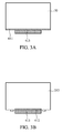
- Figs. 3A and 3B show a top view and a bottom view of the display device 1.
- the outer surface 21 comprises a lateral side 211 and a bottom side 212, and the second adhesive 43 is attached to the bottom side 212 of the outer surface 21.
- the first adhesive 42 is partially between the film base 41 and the upper surface 111.
- the second adhesive 43 is located between the film base 41 and the bottom side 212.
- the receiving space R is formed by the intermediate portion 413 and the lateral side 211.
- a rib 213 is formed on the lateral side 211, and the circuit board 30 is disposed on the rib 213.
- the rib 213 and the circuit board 30 are located in the receiving space R.
- the rib 213 can be integrally formed on the lateral side 211.
- the elements thereof can be properly fixed, and the reworking problem due to the tape being attached to the circuit board is prevented.
- the display device 1 further comprises a plastic frame 50 located between the display panel 10 and the back frame 20.
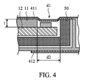
- a width d1 of the cover film 40 between the first substrate 11 and the plastic frame 50 is shorter than a sum of the a distance d2 between the first substrate 11 and the plastic frame 50 and double a thickness t of the first substrate 11. Therefore, the welding or integrated circuit below the panel can be protected, and the circuits on the left and right sides can also be protected.
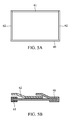
- the display device 1 further comprises a first gummed tape 61 and a second gummed tape 62, which cover and are attached to the outer surface 21 and other edges of the upper surface 111.
- a first gummed tape 61 and a second gummed tape 62 which cover and are attached to the outer surface 21 and other edges of the upper surface 111.
- an end of the second gummed tape 62 is attached to the first gummed tape 61, and the cover film 40 is attached to the other end of the second gummed tape 62 to prevent the second gummed tape 62 from easily becoming detached.
- a plurality of lead angle structures 63 are formed on the ends of the first gummed tape 61, the second gummed tape 62 and the cover film 40.
- the lead angle structures 63 are located on the bottom side 212.
- the back frame 20 further comprises a plurality of protrusions 22 formed on the lateral side.
- a plurality of notches 64 are formed on the first gummed tape 61, the second gummed tape 62 and the cover film 40 corresponding to the protrusions 22.
- Each notch 64 has a length, and the length of each notch 64 is greater than a length of each protrusion 22.
- the a width of the cover film 40, the first gummed tape 61 and second gummed tape 62 attached to the upper surface 111 differs from a width of the cover film 40, the first gummed tape 61 and second gummed tape 62 attached to the bottom side 212. Therefore, the integrated circuit and the wire can be protected, or the width of the frame can be decreased.
- the display 1 further comprises a polarizing film 70, wherein a width of the cover film 40, the first gummed tape 61 and second gummed tape 62 attached to the upper surface 111 is shorter than or equal to a horizontal distance between an edge of the polarizing film 70 and an edge of the first substrate 11.
- Fig. 7 shows a display device 1' of another embodiment of the invention, wherein the receiving space R' is formed by the intermediate portion 413 and the bottom side 212.
- the circuit board 30 is disposed on the bottom side 212.
Landscapes
- Physics & Mathematics (AREA)
- Nonlinear Science (AREA)
- Engineering & Computer Science (AREA)
- General Physics & Mathematics (AREA)
- Microelectronics & Electronic Packaging (AREA)
- Optics & Photonics (AREA)
- Crystallography & Structural Chemistry (AREA)
- Chemical & Material Sciences (AREA)
- Mathematical Physics (AREA)
- Theoretical Computer Science (AREA)
- Devices For Indicating Variable Information By Combining Individual Elements (AREA)
- Liquid Crystal (AREA)
- Measurement Of The Respiration, Hearing Ability, Form, And Blood Characteristics Of Living Organisms (AREA)
- Image Input (AREA)
Abstract
A display device is provided, including a display panel (10), a back frame (20), a circuit board (30) and a cover film (40,41,411,412,413,42,43). The display panel includes a first substrate (11) and a second substrate (12), wherein the first substrate includes an upper surface (111). The back frame (20) supports the display panel (10) and includes an outer surface (21). The cover film (40) includes a film base (41), a first adhesive (42) and a second adhesive (43). The film base includes a first portion (411), a second portion (412) and an intermediate portion (413) located therebetween, wherein the film base covers an edge of the upper surface (111) and a portion of the outer surface (21). The first adhesive (42) is disposed on the first portion (411) and is attached to the edge of the upper surface (111). The second adhesive (43) is disposed on the second portion (412) and is attached to the outer surface (21), wherein the intermediate portion (413) and the outer surface (21) define a receiving space (R) receiving the circuit board (30).

Description
- This Application claims priority of Taiwan Patent Application No.
102138013, filed on Oct. 22, 2013 - The present invention relates to a display device, and in particular to a display device utilized in thin electronic equipment.
- To satisfy the requirements on thin electronic equipment, common display devices omit the front frame, and the panel, the plastic frame and the back frame are fixed by gummed tape. However, improper tape attachment may cause uneven attachment, and the tape can easily become detached. Additionally, the gummed tape may be attached to the circuit board, and cannot be reworked.
- It is an object of the present invention to provide an enhanced display device, wherein the elements thereof can be properly fixed more easily and in a more reliable manner. A further problem to be solved is to prevent the afore-mentioned reworking problem due to the tape being attached to the circuit board.
- The above problems are solved by a display device according to
claim 1. Further advantageous embodiments are the subject-matter of the dependent claims. - According to the present invention a display device is provided, which includes or comprises a display panel, a back frame, a circuit board and a cover film. The display panel includes a first substrate and a second substrate, wherein the first substrate includes an upper surface. The back frame supports the display panel and comprises an outer surface. The circuit board is electrically connected to the display panel. The cover film includes a film base, a first adhesive and a second adhesive. The film base includes a first portion, a second portion and an intermediate portion located between the first portion and the second portion, wherein the film base covers an edge of the upper surface, a portion of the outer surface and the circuit board. The first adhesive is disposed on the first portion and is attached to the edge of the upper surface. The second adhesive is disposed on the second portion and is attached to the outer surface, wherein the intermediate portion and the outer surface define a receiving space, and the circuit board is received in the receiving space.
- Utilizing the display device of the embodiment of the invention, the elements thereof can be properly fixed, and the reworking problem due to the tape being attached to the circuit board is prevented.
- A detailed description is given in the following embodiments with reference to the accompanying drawings.
- The present invention can be more fully understood by reading the subsequent detailed description and examples with references made to the accompanying drawings, wherein:
-
Fig. 1 shows the display device of an embodiment of the invention; -
Fig. 2 shows the detailed structure of the cover film of the embodiment of the invention; -
Fig. 3A shows the top view of the display device of the embodiment of the invention; -
Fig. 3B shows the bottom view of the display device of the embodiment of the invention; -
Fig. 4 is an enlarged view of the display device of the embodiment of the invention; -
Figs. 5A and 5B show the gummed tape attached to the display device of the embodiment of the invention; -
Fig. 6 shows the detailed structure of the gummed tape of the embodiment of the invention; -
Fig. 7 shows the display device of another embodiment of the invention. - The following description is of the best-contemplated mode of carrying out the invention. This description is made for the purpose of illustrating the general principles of the invention and should not be taken in a limiting sense. The scope of the invention is best determined by reference to the appended claims.
-
Fig. 1 shows adisplay device 1 of an embodiment of the invention, comprising adisplay panel 10, aback frame 20, acircuit board 30 and a cover film, 40. Thedisplay panel 10 comprises afirst substrate 11 and asecond substrate 12, wherein thefirst substrate 11 comprises anupper surface 111. Theback frame 20 supports thedisplay panel 10 and comprises anouter surface 21. Thecircuit board 30 is electrically connected to thedisplay panel 10. Thecover film 40 comprises afilm base 41, afirst adhesive 42 and asecond adhesive 43. Thefilm base 41 comprises afirst portion 411, asecond portion 412 and anintermediate portion 413 located between thefirst portion 411 and thesecond portion 412. Thefilm base 41 covers an edge of theupper surface 111, a portion of theouter surface 21 and thecircuit board 30. Thefirst adhesive 42 is disposed on thefirst portion 411 and is attached to the edge of theupper surface 111. Thesecond adhesive 43 is disposed on thesecond portion 412 and is attached to theouter surface 21, wherein theintermediate portion 413 and theouter surface 21 define a receiving space R, and thecircuit board 30 is received in the receiving space R. -
Fig. 2 shows detailed structure of thecover film 40, wherein a length of thefirst adhesive 42 in a first direction X is longer than a length of thesecond adhesive 43 in the first direction X. A length of thefirst portion 411 in the first direction X is longer than a length of thesecond portion 412 in the first direction X. The adhesive ability of theintermediate portion 413 differs from an adhesive ability of thefirst portion 411, and the adhesive ability of theintermediate portion 413 differs from an adhesive ability of thesecond portion 412. In one embodiment of the invention, no adhesive is attached to theintermediate portion 413. Therefore, the adhesive ability of theintermediate portion 413 is poorer than the adhesive ability of thefirst portion 411, and the adhesive ability of theintermediate portion 413 is poorer than the adhesive ability of thesecond portion 412. -
Figs. 3A and 3B show a top view and a bottom view of thedisplay device 1. With reference toFig. 1 and3B , theouter surface 21 comprises alateral side 211 and abottom side 212, and thesecond adhesive 43 is attached to thebottom side 212 of theouter surface 21. - With reference to
Fig. 1 , thefirst adhesive 42 is partially between thefilm base 41 and theupper surface 111. Thesecond adhesive 43 is located between thefilm base 41 and thebottom side 212. - With reference to
Fig. 1 , the receiving space R is formed by theintermediate portion 413 and thelateral side 211. Arib 213 is formed on thelateral side 211, and thecircuit board 30 is disposed on therib 213. Therib 213 and thecircuit board 30 are located in the receiving space R. Therib 213 can be integrally formed on thelateral side 211. - Utilizing the display device of the embodiment of the invention, the elements thereof can be properly fixed, and the reworking problem due to the tape being attached to the circuit board is prevented.
- With reference to
Fig. 1 , in one embodiment, thedisplay device 1 further comprises aplastic frame 50 located between thedisplay panel 10 and theback frame 20. With reference toFig. 4 , a width d1 of thecover film 40 between thefirst substrate 11 and theplastic frame 50 is shorter than a sum of the a distance d2 between thefirst substrate 11 and theplastic frame 50 and double a thickness t of thefirst substrate 11. Therefore, the welding or integrated circuit below the panel can be protected, and the circuits on the left and right sides can also be protected. - With reference to
Fig. 5A , in one embodiment, thedisplay device 1 further comprises a first gummedtape 61 and a second gummedtape 62, which cover and are attached to theouter surface 21 and other edges of theupper surface 111. With reference toFig. 5B , in one embodiment, an end of the second gummedtape 62 is attached to the first gummedtape 61, and thecover film 40 is attached to the other end of the second gummedtape 62 to prevent the second gummedtape 62 from easily becoming detached. - With reference to
Fig. 6 , in one embodiment, a plurality oflead angle structures 63 are formed on the ends of the first gummedtape 61, the second gummedtape 62 and thecover film 40. Thelead angle structures 63 are located on thebottom side 212. Theback frame 20 further comprises a plurality ofprotrusions 22 formed on the lateral side. A plurality ofnotches 64 are formed on the first gummedtape 61, the second gummedtape 62 and thecover film 40 corresponding to theprotrusions 22. Eachnotch 64 has a length, and the length of eachnotch 64 is greater than a length of eachprotrusion 22. Thus, the attachment of the first and the second gummed tape can be smoother. - In one embodiment, the a width of the
cover film 40, the first gummedtape 61 and second gummedtape 62 attached to theupper surface 111 differs from a width of thecover film 40, the first gummedtape 61 and second gummedtape 62 attached to thebottom side 212. Therefore, the integrated circuit and the wire can be protected, or the width of the frame can be decreased. - With reference to
Fig. 1 , in one embodiment, thedisplay 1 further comprises apolarizing film 70, wherein a width of thecover film 40, the first gummedtape 61 and second gummedtape 62 attached to theupper surface 111 is shorter than or equal to a horizontal distance between an edge of thepolarizing film 70 and an edge of thefirst substrate 11. -
Fig. 7 shows a display device 1' of another embodiment of the invention, wherein the receiving space R' is formed by theintermediate portion 413 and thebottom side 212. In this embodiment, thecircuit board 30 is disposed on thebottom side 212. - Use of ordinal terms such as "first", "second", "third", etc., in the claims to modify a claim element does not by itself connote any priority, precedence, or order of one claim element over another or the temporal order in which acts of a method are performed, but are used merely as labels to distinguish one claim element having a certain name from another element having the same name (but for use of the ordinal term) to distinguish the claim elements.
- While the invention has been described by way of example and in terms of the preferred embodiments, it is to be understood that the invention is not limited to the disclosed embodiments. On the contrary, it is intended to cover various modifications and similar arrangements (as would be apparent to those skilled in the art). Therefore, the scope of the appended claims should be accorded the broadest interpretation so as to encompass all such modifications and similar arrangements.
Claims (15)
- A display device, comprising:a display panel, comprising a first substrate and a second substrate, wherein the first substrate comprises an upper surface;a back frame, supporting the display panel and comprising an outer surface;a circuit board, electrically connected to the display panel; anda cover film, comprising:a film base, comprising a first portion, a second portion and an intermediate portion located between the first portion and the second portion, wherein the film base covers an edge of the upper surface, a portion of the outer surface and the circuit board;a first adhesive, disposed on the first portion and attached to the edge of the upper surface; anda second adhesive, disposed on the second portion and attached to the outer surface, wherein the intermediate portion and the outer surface define a receiving space, and the circuit board is received in the receiving space.
- The display device as claimed in claim 1, wherein an adhesive ability of the intermediate portion differs from an adhesive ability of the first portion, and the adhesive ability of the intermediate portion differs from an adhesive ability of the second portion.
- The display device as claimed in claim 1 or 2, wherein an adhesive ability of the intermediate portion is poorer than an adhesive ability of the first portion, and the adhesive ability of the intermediate portion is poorer than an adhesive ability of the second portion.
- The display device as claimed in any of the preceding claims, wherein a length of the first adhesive in a first direction is longer than a length of the second adhesive in the first direction.
- The display device as claimed in any of the preceding claims, wherein the outer surface comprises a lateral side and a bottom side, and the second adhesive is attached to the bottom side.
- The display device as claimed in claim 5, wherein the receiving space is formed by the intermediate portion and the lateral side.
- The display device as claimed in claim 5, wherein the receiving space is formed by the intermediate portion and the bottom side.
- The display device as claimed in any of the preceding claims, further comprising a first gummed tape and a second gummed tape, covering and attached to the outer surface and other edges of the upper surface.
- The display device as claimed in claim 8, wherein an end of the second gummed tape is attached to the first gummed tape, and the cover film is attached to the other end of the second gummed tape.
- The display device as claimed in claim 8, wherein a plurality of lead angle structures are formed on ends of the first or second gummed tape, and the lead angle structures are located on the bottom side.
- The display device as claimed in any of claims 8 to 10, wherein the back frame comprises a plurality of protrusions formed on the lateral side, and the first or second gummed tape has a plurality of notches corresponding to the protrusions, and a length of each notch is greater than a length of each protrusion.
- The display device as claimed in any of claims 8 to 11, wherein a width of the cover film, the first gummed tape and second gummed tape attached to the upper surface differs from a width of the cover film, the first gummed tape and second gummed tape attached to the bottom side.
- The display device as claimed in any of claims 8 to 12, further comprising a polarizing film, wherein a width of the cover film, the first gummed tape and second gummed tape attached to the upper surface is shorter than or equal to a horizontal distance between an edge of the polarizing film and an edge of the first substrate.
- The display device as claimed in any of the preceding claims, wherein no adhesive is attached to the intermediate portion.
- The display device as claimed in any of the preceding claims, comprising a plastic frame, located between the display panel and the back frame, a width of the cover film between the first substrate and the plastic frame is shorter than a sum of the a distance between the first substrate and the plastic frame and double a thickness of the first substrate.
Applications Claiming Priority (1)
| Application Number | Priority Date | Filing Date | Title |
|---|---|---|---|
| TW102138013A TWI512360B (en) | 2013-10-22 | 2013-10-22 | Display device |
Publications (1)
| Publication Number | Publication Date |
|---|---|
| EP2866077A1 true EP2866077A1 (en) | 2015-04-29 |
Family
ID=50064451
Family Applications (1)
| Application Number | Title | Priority Date | Filing Date |
|---|---|---|---|
| EP20140153764 Withdrawn EP2866077A1 (en) | 2013-10-22 | 2014-02-04 | Display device |
Country Status (6)
| Country | Link |
|---|---|
| US (1) | US9565778B2 (en) |
| EP (1) | EP2866077A1 (en) |
| JP (1) | JP3194674U (en) |
| KR (1) | KR101721736B1 (en) |
| CN (1) | CN204117503U (en) |
| TW (1) | TWI512360B (en) |
Families Citing this family (4)
| Publication number | Priority date | Publication date | Assignee | Title |
|---|---|---|---|---|
| CN108933200B (en) * | 2018-07-09 | 2020-03-27 | 京东方科技集团股份有限公司 | Packaging structure |
| CN110174801B (en) * | 2019-05-30 | 2024-03-26 | 武汉华星光电技术有限公司 | Display module |
| WO2021225189A1 (en) * | 2020-05-07 | 2021-11-11 | 엘지전자 주식회사 | Display device |
| CN118301928A (en) * | 2023-01-05 | 2024-07-05 | 新加坡商群丰骏科技股份有限公司 | Electronic device and method of manufacturing the same |
Citations (4)
| Publication number | Priority date | Publication date | Assignee | Title |
|---|---|---|---|---|
| US20070146612A1 (en) * | 2005-12-26 | 2007-06-28 | Nec Lcd Technologies, Ltd. | Liquid crystal display apparatus and method for dust prevention of liquid crystal display apparatus |
| US20090128733A1 (en) * | 2007-11-20 | 2009-05-21 | Mitsubishi Electric Corporation | Liquid crystal display device |
| JP2010151897A (en) * | 2008-12-24 | 2010-07-08 | Citizen Holdings Co Ltd | Electric display and method of manufacturing the same |
| US20120169963A1 (en) * | 2010-12-29 | 2012-07-05 | Samsung Mobile Display Co., Ltd. | Liquid crystal display apparatus |
Family Cites Families (6)
| Publication number | Priority date | Publication date | Assignee | Title |
|---|---|---|---|---|
| TWI381214B (en) * | 2009-01-20 | 2013-01-01 | Au Optronics Corp | Backlight module and display apparatus |
| JP2011048330A (en) | 2009-07-31 | 2011-03-10 | Kyowa Kasei Kk | Advertisement and bulletin display |
| KR101580492B1 (en) * | 2009-09-17 | 2015-12-29 | 엘지디스플레이 주식회사 | Shading tape structure and shading tape attachment method |
| US9275561B2 (en) * | 2010-11-09 | 2016-03-01 | Samsung Display Co., Ltd. | Optical adhesive film and flat panel display device having the same |
| JP5928020B2 (en) * | 2012-03-13 | 2016-06-01 | ソニー株式会社 | Display device |
| CN102831826B (en) * | 2012-08-27 | 2014-07-23 | 深圳市华星光电技术有限公司 | Display device |
-
2013
- 2013-10-22 TW TW102138013A patent/TWI512360B/en active
-
2014
- 2014-02-04 EP EP20140153764 patent/EP2866077A1/en not_active Withdrawn
- 2014-09-22 JP JP2014005048U patent/JP3194674U/en not_active Expired - Lifetime
- 2014-09-22 CN CN201420546846.0U patent/CN204117503U/en not_active Expired - Lifetime
- 2014-09-23 US US14/493,424 patent/US9565778B2/en active Active
- 2014-10-16 KR KR1020140139581A patent/KR101721736B1/en active Active
Patent Citations (4)
| Publication number | Priority date | Publication date | Assignee | Title |
|---|---|---|---|---|
| US20070146612A1 (en) * | 2005-12-26 | 2007-06-28 | Nec Lcd Technologies, Ltd. | Liquid crystal display apparatus and method for dust prevention of liquid crystal display apparatus |
| US20090128733A1 (en) * | 2007-11-20 | 2009-05-21 | Mitsubishi Electric Corporation | Liquid crystal display device |
| JP2010151897A (en) * | 2008-12-24 | 2010-07-08 | Citizen Holdings Co Ltd | Electric display and method of manufacturing the same |
| US20120169963A1 (en) * | 2010-12-29 | 2012-07-05 | Samsung Mobile Display Co., Ltd. | Liquid crystal display apparatus |
Also Published As
| Publication number | Publication date |
|---|---|
| TW201516519A (en) | 2015-05-01 |
| TWI512360B (en) | 2015-12-11 |
| KR101721736B1 (en) | 2017-03-30 |
| JP3194674U (en) | 2014-12-04 |
| US20150109742A1 (en) | 2015-04-23 |
| KR20150046732A (en) | 2015-04-30 |
| CN204117503U (en) | 2015-01-21 |
| US9565778B2 (en) | 2017-02-07 |
Similar Documents
| Publication | Publication Date | Title |
|---|---|---|
| US11114632B2 (en) | Display panels and methods for manufacturing the same | |
| EP3550543B1 (en) | Flexible display screen and flexible display apparatus | |
| US11058000B1 (en) | Flexible display device | |
| US11081059B2 (en) | Display panels and display devices | |
| EP3683650B1 (en) | Display screen assembly and mobile terminal | |
| US8542481B2 (en) | Liquid crystal display module for portable terminal | |
| US10249594B2 (en) | Display device and method for assembling the same | |
| US9735221B2 (en) | Display module | |
| US9897739B2 (en) | Optical film, backlight module, and display device | |
| US9733673B2 (en) | Display module | |
| US20120127639A1 (en) | Display device | |
| US9565778B2 (en) | Display device | |
| US12045414B2 (en) | Display device | |
| US10523799B1 (en) | Flexible display panel and electronic device | |
| CN108922407B (en) | Display screens and display devices | |
| US11277904B2 (en) | Circuit board, backlight module comprising the circuit board, and display device | |
| US8952254B2 (en) | Electronic device cover | |
| KR102425659B1 (en) | Structural Components and Mobile Terminals | |
| US10345634B2 (en) | Display apparatus | |
| US9575344B2 (en) | Display module | |
| US20150016041A1 (en) | Electronic apparatus and module | |
| US8164914B2 (en) | Circuit board fixing device | |
| US10677276B2 (en) | Fixing structure and fixing method | |
| CN113113457A (en) | Display panel | |
| US9261265B1 (en) | Backlight display device |
Legal Events
| Date | Code | Title | Description |
|---|---|---|---|
| PUAI | Public reference made under article 153(3) epc to a published international application that has entered the european phase |
Free format text: ORIGINAL CODE: 0009012 |
|
| 17P | Request for examination filed |
Effective date: 20140204 |
|
| AK | Designated contracting states |
Kind code of ref document: A1 Designated state(s): AL AT BE BG CH CY CZ DE DK EE ES FI FR GB GR HR HU IE IS IT LI LT LU LV MC MK MT NL NO PL PT RO RS SE SI SK SM TR |
|
| AX | Request for extension of the european patent |
Extension state: BA ME |
|
| STAA | Information on the status of an ep patent application or granted ep patent |
Free format text: STATUS: THE APPLICATION IS DEEMED TO BE WITHDRAWN |
|
| 18D | Application deemed to be withdrawn |
Effective date: 20151030 |