EP2866027A1 - Eddy current sensor with linear drive conductor - Google Patents
Eddy current sensor with linear drive conductor Download PDFInfo
- Publication number
- EP2866027A1 EP2866027A1 EP20140189946 EP14189946A EP2866027A1 EP 2866027 A1 EP2866027 A1 EP 2866027A1 EP 20140189946 EP20140189946 EP 20140189946 EP 14189946 A EP14189946 A EP 14189946A EP 2866027 A1 EP2866027 A1 EP 2866027A1
- Authority
- EP
- European Patent Office
- Prior art keywords
- eddy current
- sense
- sense coil
- current sensor
- layer
- Prior art date
- Legal status (The legal status is an assumption and is not a legal conclusion. Google has not performed a legal analysis and makes no representation as to the accuracy of the status listed.)
- Granted
Links
Images


Classifications
-
- G—PHYSICS
- G01—MEASURING; TESTING
- G01N—INVESTIGATING OR ANALYSING MATERIALS BY DETERMINING THEIR CHEMICAL OR PHYSICAL PROPERTIES
- G01N27/00—Investigating or analysing materials by the use of electric, electrochemical, or magnetic means
- G01N27/72—Investigating or analysing materials by the use of electric, electrochemical, or magnetic means by investigating magnetic variables
- G01N27/82—Investigating or analysing materials by the use of electric, electrochemical, or magnetic means by investigating magnetic variables for investigating the presence of flaws
- G01N27/90—Investigating or analysing materials by the use of electric, electrochemical, or magnetic means by investigating magnetic variables for investigating the presence of flaws using eddy currents
- G01N27/9006—Details, e.g. in the structure or functioning of sensors
Definitions
- the subject matter disclosed herein relates to multi-layer sensors used in eddy current probes and, in particular, to a sensor design having a linear drive conductor.
- Eddy current probes are a form of nondestructive test devices that can be used to inspect test objects made of electrically conductive material to detect and analyze flaws in the test objects. Nondestructive testing allows an inspection technician to maneuver an eddy current probe over a surface of the test object during a test scan.
- a magnetic field is used to induce an electrical current in the test object.
- the magnetic field is typically generated by one or more drive circuits typically in the form of electrically conductive drive coils, or windings, in the eddy current sensor.
- an electrical current travels through the drive coil, or coils, which generates a magnetic field that passes into the test object and induces an electrical current in the test object called an eddy current.
- the eddy current in the test object will itself generate a detectable magnetic field. This responsive magnetic field is then detected by a sense coil, or coils, and is analyzed by programmed electronics in the eddy current probe.
- the sense coils will detect this as a varying impedance.
- the sense coils will generate electrical signals that represent physical characteristics of the defect. By analyzing these electrical signals, various characteristics of the defect (e.g., location, size) can be determined.
- the impedance difference detected by the sense coils can be converted into a two-dimensional impedance data display.
- Typical eddy current sensors utilize complementary, multi-turn coils in driving and sensing circuits which together form a relatively large footprint and are sensitive to noise effects caused by scanning edges of the test object.
- a multi-layer eddy current sensor includes a sense coil for detecting an eddy current, and a drive conductor for inducing the eddy current.
- the drive conductor comprises a substantially straight conducting portion that traverses the entire width of the sense coil.
- an eddy current sensor in one embodiment, includes a first sense coil for detecting an eddy current, wherein the first sense coil comprises a first axis and a first width.
- the eddy current sensor also includes a first drive conductor for inducing the eddy current, the first drive conductor spaced apart from the first sense coil by an insulator layer.
- the first drive conductor includes a substantially straight conducting portion that traverses the first width of the first sense coil.
- the eddy current sensor includes a first plurality of sense coils for detecting an eddy current, wherein each of the first plurality of sense coils is disposed in a first layer of the eddy current sensor and arranged in a first row therein, each of the first plurality of sense coils comprising a first axis and a first width.
- the eddy current sensor also includes a first drive conductor for inducing the eddy current, wherein the first drive conductor is disposed in a second layer of the eddy current sensor and spaced apart from the first plurality of sense coils by an insulator layer.
- the first drive conductor comprises a substantially straight conducting portion that traverses each of the first widths of the first plurality of sense coils in the first row.
- the eddy current sensor includes a first sense coil for detecting an eddy current, wherein the first sense coil comprises a first axis and a first width.
- the eddy current sensor also includes a first drive conductor for inducing the eddy current, the first drive conductor spaced apart from the first sense coil by an insulator layer, wherein the first drive conductor comprises a substantially straight conducting portion that traverses the width of the first sense coil on a first longitudinal axis.
- the eddy current sensor includes a second drive conductor for inducing the eddy current, the second drive conductor spaced apart from the first sense coil by the insulator layer, wherein the second drive conductor comprises a substantially straight conducting portion that traverses the width of the first sense coil on a second longitudinal axis.
- FIG. 1 illustrates a top view of an exemplary embodiment of an eddy current sensor 100 including a drive conductor 104 and a first sense coil 106.
- the eddy current sensor 100 may be used to construct an eddy current probe having one or more of the eddy current sensors 100 formed therein.
- the overall construction of the eddy current sensor 100 utilizes a multi-layer flexible printed circuit.
- the drive conductor 104 is formed in one layer of the flexible printed circuit while the first sense coil 106 is formed in another layer thereof.
- the drive conductor 104 may be formed in a substantially straight line in the portion of the drive conductor 104 that traverses the width 109 of the first sense coil 106.
- the drive conductor 104 may have a width 107 ranging from about 0.25 mm to over about 8.0 mm.
- the sense coil may be formed in one or more layers of the multi-layer printed circuit, as will be explained below.
- a width 109 of the first sense coil 106 may vary from about 1.0 mm to over about 5.0 mm as measured at the outermost edges of the first sense coil 106. In one embodiment, the width 109 of the first sense coil 106 is about 1.6 mm and the width 107 of the drive conductor 104 is about 0.38 mm.
- a center of the first sense coil 106 comprises an axis 105 that is perpendicular to a plane containing the first sense coil 106.
- the drive conductor 104 and the first sense coil 106 are positioned, in their respective layers of the multi-layer printed circuit, such that the axis 105 of the first sense coil 106 intersects the drive conductor 104, as illustrated in FIG. 1 .
- the first sense coil 106 is positioned vertically below the drive conductor 104, in their respective layers of the multi-layer printed circuit, such that the first sense coil 106 is situated between the drive conductor 104 and the test object during a scan of the test object.
- the drive conductor 104 is positioned vertically below the first sense coil 106, in their respective layers of the multi-layer printed circuit as illustrated in FIG. 1 , such that the drive conductor 104 is situated between the first sense coil 106 and the test object during a scan of the test object.
- the first sense coil 106 terminates at electrical leads 108, 110 which may be connected to electronics of an eddy current probe for performing test scans.
- the drive conductor 104 is similarly connected to the eddy current probe, wherein the eddy current probe controllably drives an electric current, having a selected magnitude and frequency, through the drive conductor 104.
- the electrical lead 108 is formed in a same layer of the multi-layer printed circuit as the first sense coil 106.
- Electrical lead 110 is formed in a different layer of the multi-layer printed circuit than the electrical lead 108, and is electrically connected to first sense coil 106 by a via 115.
- the multi-layered printed circuit generally comprises variously alternating layers of an insulator, an adhesive, and a conductor.
- the conductor layers of the multi-layer printed circuit comprise the drive conductor 104 and the first sense coil 106 just described.
- an eddy current probe drives an electric current at a selected frequency and amplitude through the drive conductor 104 to induce an eddy current in a test object for performing a scan thereof.
- the induced eddy current in the test object generates a measureable magnetic field that is detected by the first sense coil 106. This detection is made more sensitive with an increased number of windings in the first sense coil 106.
- Each turn, or winding, of the first sense coil 106 detects the magnetic field by generating a small voltage in response to the eddy current magnetic field, such that each turn of the coil contributes (adds) an amount of voltage to an overall sense coil voltage signal which can then be analyzed by electronics of the eddy current probe.
- a width of each winding of the first sense coil 106 is about 0.05 mm with an equivalent spacing between the windings.
- the overall width 109 of the first sense coil 106 is equal to about 1.6 mm, as illustrated in the first sense coil 106 of FIG. 1 . If the windings of the first sense coil 106 have a smaller width of about 0.025 mm with an equivalent spacing between turns of the first sense coil 106, the number of turns would increase by about 2x, thereby increasing the sensitivity of the first sense coil 106.
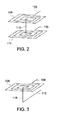
- FIG. 2 shows an isolated view of one embodiment of the eddy current sensor 100 wherein a first sense coil 106 is electrically connected to a second sense coil 111.
- Each of the sense coils 106, 111 is formed in a separate layer of a flexible multi-layer printed circuit, and are electrically connected by a via 115 formed through an intervening layer of the multi-layer printed circuit, which intervening layer may be an insulator layer.
- Electrical lead 108 is formed in the same layer of the multi-layer printed circuit as the first sense coil 106, while electrical lead 110 is formed in the same layer of the multi-layer printed circuit as the second sense coil 111.
- the insulator layer which will be described in more detail below, maintains the sense coils 106, 111 in a vertical, substantially parallel, spaced apart relationship, as illustrated in FIG. 2 .
- FIG. 3 shows an isolated view of one embodiment of the eddy current sensor 100 comprising a first sense coil 106 electrically connected to electrical lead 108 formed in the same layer of the multi-layer printed circuit as the first sense coil 106, and to electrical lead 110 formed in a separate layer of the multi-layer printed circuit.
- the first sense coil 106 is electrically connected to electrical lead 110 by a via 115 formed through an intervening layer of the multi-layer printed circuit, which intervening layer may be an insulator layer.
- FIG. 4 illustrates an exemplary configuration of a flexible multi-layer printed circuit 400 arranged to create the eddy current sensor 100 as illustrated in FIG. 1 .
- the multi-layer printed circuit 400 comprises insulator layers 421-425, conductor layers 426-428, and adhesive layers 416.
- the thickness of the adhesive layers 416 are shown in minimized form for ease of illustration in the Figure, however, the thickness of the adhesive layers 416 is similar to that of the insulator layers 421-425, which may range from about 0.01 mm to about 0.1 mm.
- FIG. 4 may be considered as a generalized side view of the eddy current sensor 100, and is not drawn to specifically illustrate a cross-section of the eddy current sensor 100 of FIG. 1 .
- the various layers 421-428 of the multi-layer printed circuit of FIG. 4 may be referred to throughout the present disclosure to provide a structural reference for the various embodiments described herein.
- An uppermost conductor layer 426 of the multi-layer printed circuit 400 comprises the drive conductor 104 described above.
- the conductor layer 426 may comprise one or more of drive conductors 104.
- Another conductor layer 427 comprises a first sense coil 106 formed as a planar, square shaped coil, within which layer 427 may also include an electrical lead 108 of the first sense coil 106 ( FIGS. 1-3 ).
- One or more additional first sense coils 106 may be formed in conductor layer 427 each with a corresponding electrical lead 108.
- the sense coils 106 can have various configurations other than those shown, such as round, triangular, oval or other shape, and can include any combination of features disclosed herein and known in the art.
- the second sense coil 111 connected to electrical lead 110 formed in the same conductor layer 428 as the sense coil 111, is also connected to the first sense coil 106 by a via 415 formed between the conductor layers 427, 428 through an intervening insulator layer 424.
- the via 415 may be formed proximate to the axes 405 of the sense coils 106, 111.
- One or more additional second sense coils 111 may be formed in conductor layer 428, each with a corresponding electrical lead 110.
- electrical lead 110 formed in a lower conductor layer 428 of the multi-layer printed circuit is connected to the first sense coil 106 by a via 415 formed between the conductor layers 427, 428 through an intervening insulator layer 424.
- the via 415 may be formed proximate to the axis 405 of the first sense coil 106.
- the insulator layers 421-425 are used to spatially separate and selectively electrically isolate the conductor layers 426-428 including the drive conductor 104 and the sense coils 106, 111 formed therein.
- the insulator layers 421-425 may be comprised of a polyimide such as Kapton tape, or Teflon tape.
- the conductor layers 426-428, used for forming the drive conductor 104 and the sense coils 106, 111, may comprise a metal such as copper formed by a deposition process or copper tape adhered between the insulator layers.
- the copper layers may comprise a thickness of about 5 ⁇ m.
- Adhesive layers 416 are placed between each insulator layer, 421-425, and each conductor layer 426-428.
- each of the insulator layers 421-425 and the adhesive layers 416 may be about 0.013 mm thick.
- the conductor layers 426-428 may each be about 5 ⁇ m thick.
- each of the layers 421-428 of the multi-layer printed circuit 400 may be individually fabricated and, as the layers 421-428 are stacked, secured in place using an adhesive coating or double-sided adhesive tape between each assembled layer 421-428.
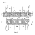
- FIG. 5 illustrates an eddy current sensor array 500 comprising a first and second plurality of sense coils 506, 508 and a plurality of drive conductors 503, 504, operative as a plurality of individual eddy current sensors as described above with respect to FIG. 1 .
- a first plurality of sense coils 506 are arranged in one row while a second plurality of sense coils 508 are arranged in a second row.
- Each of the first plurality of sense coils 506 in one row comprise an axis 505 and a width 509, while each of the second plurality of sense coils 508 in the second row comprise an axis 507 and a width 510.
- two rows of sense coils 506, 508 each comprise sixty-four sense coils for a total of one hundred twenty eight eddy current sensors 100 ( FIG. 1 ) in one eddy current probe.
- the drive conductors 503, 504 and their corresponding sense coils 506, 508 may be formed in the multi-layer printed circuit with the sense coils 506, 508 vertically above their corresponding drive conductor 503, 504, or vice versa.
- the first plurality of sense coils 506 are positioned with respect to the first drive conductor 503 such that each of their axes 505 intersect the first drive conductor 503 while the second plurality of sense coils 508 are positioned with respect to the second drive conductor 504 such that each of their axes 507 intersect the second drive conductor 504.
- the drive conductors 503, 504 may be formed in a substantially straight line over their entire length, i.e., over the entire combined widths 509, 510 of their corresponding sense coils 506, 508, respectively.
- the drive conductors 503, 504 may be formed in a substantially straight line at least in the portion of the drive conductors 503, 504 that traverse the widths 509, 510 of the first and second plurality of sense coils 506, 508, respectively.
- the first and second plurality of sense coils 506, 508 may be formed in the same conductor layer 427 of the multi-layer printed circuit ( FIG. 4 ).
- the first and second plurality of sense coils sense coils 506, 508 are configured to detect eddy currents in a test object that are induced therein by the drive conductors 503, 504.
- the eddy current sensor array 500 comprises individual sense coils 506, 508 and corresponding drive conductors 503, 504 that cooperate in a similar fashion as the exemplary eddy current sensor 100, as explained above with reference to FIG. 1 .
- Pairs of electrical leads 511, 512 are connected to each of the first plurality of sense coils 506 while pairs of electrical leads 513, 514 are connected to each of the second plurality of sense coils 508.
- the electrical leads 511-514 transmit voltage signals generated in their attached sense coils 506, 508 to electronics of an eddy current probe for analysis therein, such as for determining the location and size of a flaw in a scanned
- the first drive conductor 503 may be formed in one conductor layer 426 of the multi-layer printed circuit ( FIG. 4 ), which operates in conjunction with the corresponding first plurality of sense coils 506 arranged in one row and formed in another conductor layer 427 of the multi-layer printed circuit.
- the first and second drive conductors 503, 504 may be formed in the conductor layer 426 and each operated in conjunction with one corresponding row of sense coils 506, 508 as illustrated in FIG. 5 .
- the plurality of rows of sense coils 506, 508 may be formed in a common conductor layer 427 of the multi-layer printed circuit 400.
- each of the sense coils 506, 508 may be formed as a single sense coil in one conductor layer 427 of the multi-layer printed circuit 400 ( FIG. 4 ), as described above in relation to FIG. 3 .
- each of the sense coils 506, 508 are connected to electrical leads, 512, 514 in another conductor layer 428, respectively, by a via 515, 516, respectively, that passes through an intervening insulator layer 424.
- each of the sense coils 506, 508 may be formed as first and second sense coils formed in two separate conductor layers 427, 428 of the multi-layer printed circuit ( FIG. 4 ), as described above in relation to FIG. 2 .
- the first sense coils are formed in conductor layer 427 and are each electrically connected to second sense coils formed in another conductor layer 428, respectively, by a via 515, 516, respectively, that passes through the intervening insulator layer 424.
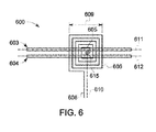
- FIG. 6 illustrates an alternative embodiment of an eddy current sensor 600.
- the eddy current sensor 600 includes a pair of drive conductors 603, 604 formed as a pair of parallel substantially straight conducting sections, and a sense coil 606 connected to electrical leads 608, 610.
- the embodiment illustrated in FIG. 6 operates and is constructed substantially the same as the exemplary embodiment of the eddy current sensor 100 of FIG. 1 , except that the drive conductor 104 is formed as a pair of parallel conductors 603, 604 that are formed in a common conductor layer 426 ( FIG. 4 ) of the multi-layer printed circuit.
- the drive conductors 603, 604, each comprise a longitudinal axis 611, 612, respectively.
- the pair of drive conductors 603, 604 are positioned such that their longitudinal axes 611, 612, are equidistant from the axis 605 of the sense coil 606 at the point where the drive conductors 603, 604 are proximate to the sense coil axis 605.
- the sense coil 606 comprises a width 609, as measured at the outermost edges of the sense coil 606, and the drive conductors 603, 604 are formed in substantially straight parallel lines at least in the portions of the drive conductors 603, 604 that traverse the width 609 of the sense coil 606.
- the sense coil 606 may be formed as a single coil embodiment as described in relation to FIG. 3 , wherein the sense coil 606 is electrically connected to electrical lead 610 formed in another conductor layer, e.g. layer 428 ( FIG. 4 ) of the multi-layer printed circuit 400, by a via 615 that passes through an intervening insulator layer 424.
- the sense coil 606 may be electrically connected to a second sense coil formed in a separate conductor layer, e.g., layer 428, of the multi-layer printed circuit 400 by a via 615 that passes through the intervening insulator layer 424 ( FIG. 4 ).
- embodiments of the invention provide a unique linear drive conductor that allows formation of an eddy current sensor with a small footprint and a self-nulling response that reduces noise.
- a technical effect is an improved inspection capability especially near an edge of a test object.
Landscapes
- Chemical & Material Sciences (AREA)
- Chemical Kinetics & Catalysis (AREA)
- Electrochemistry (AREA)
- Physics & Mathematics (AREA)
- Health & Medical Sciences (AREA)
- Life Sciences & Earth Sciences (AREA)
- Analytical Chemistry (AREA)
- Biochemistry (AREA)
- General Health & Medical Sciences (AREA)
- General Physics & Mathematics (AREA)
- Immunology (AREA)
- Pathology (AREA)
- Investigating Or Analyzing Materials By The Use Of Magnetic Means (AREA)
Abstract
Description
- The subject matter disclosed herein relates to multi-layer sensors used in eddy current probes and, in particular, to a sensor design having a linear drive conductor.
- Eddy current probes are a form of nondestructive test devices that can be used to inspect test objects made of electrically conductive material to detect and analyze flaws in the test objects. Nondestructive testing allows an inspection technician to maneuver an eddy current probe over a surface of the test object during a test scan.
- In an eddy current sensor, a magnetic field is used to induce an electrical current in the test object. The magnetic field is typically generated by one or more drive circuits typically in the form of electrically conductive drive coils, or windings, in the eddy current sensor. During operation of the probe, an electrical current travels through the drive coil, or coils, which generates a magnetic field that passes into the test object and induces an electrical current in the test object called an eddy current. The eddy current in the test object will itself generate a detectable magnetic field. This responsive magnetic field is then detected by a sense coil, or coils, and is analyzed by programmed electronics in the eddy current probe.
- If the induced eddy current passes through a flaw or defect in the test object during the scan, the induced eddy current is perturbed and the sense coils will detect this as a varying impedance. In response to detecting the varying impedance, the sense coils will generate electrical signals that represent physical characteristics of the defect. By analyzing these electrical signals, various characteristics of the defect (e.g., location, size) can be determined. The impedance difference detected by the sense coils can be converted into a two-dimensional impedance data display.
- Typical eddy current sensors utilize complementary, multi-turn coils in driving and sensing circuits which together form a relatively large footprint and are sensitive to noise effects caused by scanning edges of the test object.
- The discussion above is merely provided for general background information and is not intended to be used as an aid in determining the scope of the claimed subject matter.
- A multi-layer eddy current sensor includes a sense coil for detecting an eddy current, and a drive conductor for inducing the eddy current. The drive conductor comprises a substantially straight conducting portion that traverses the entire width of the sense coil. An advantage that may be realized in the practice of some disclosed embodiments of the eddy current sensor probe is that the drive circuit generates a self nulling magnetic field in the sense coil which reduces noise, and the overall footprint of the eddy current sensor is smaller. Interference from an edge of the test object is reduced, resulting in improved edge inspection.
- In one embodiment, an eddy current sensor is disclosed. The eddy current sensor includes a first sense coil for detecting an eddy current, wherein the first sense coil comprises a first axis and a first width. The eddy current sensor also includes a first drive conductor for inducing the eddy current, the first drive conductor spaced apart from the first sense coil by an insulator layer. The first drive conductor includes a substantially straight conducting portion that traverses the first width of the first sense coil.
- In another embodiment, the eddy current sensor includes a first plurality of sense coils for detecting an eddy current, wherein each of the first plurality of sense coils is disposed in a first layer of the eddy current sensor and arranged in a first row therein, each of the first plurality of sense coils comprising a first axis and a first width. The eddy current sensor also includes a first drive conductor for inducing the eddy current, wherein the first drive conductor is disposed in a second layer of the eddy current sensor and spaced apart from the first plurality of sense coils by an insulator layer. The first drive conductor comprises a substantially straight conducting portion that traverses each of the first widths of the first plurality of sense coils in the first row.
- In yet another embodiment, the eddy current sensor includes a first sense coil for detecting an eddy current, wherein the first sense coil comprises a first axis and a first width. The eddy current sensor also includes a first drive conductor for inducing the eddy current, the first drive conductor spaced apart from the first sense coil by an insulator layer, wherein the first drive conductor comprises a substantially straight conducting portion that traverses the width of the first sense coil on a first longitudinal axis. In addition, the eddy current sensor includes a second drive conductor for inducing the eddy current, the second drive conductor spaced apart from the first sense coil by the insulator layer, wherein the second drive conductor comprises a substantially straight conducting portion that traverses the width of the first sense coil on a second longitudinal axis.
- This brief description of the invention is intended only to provide a brief overview of subject matter disclosed herein according to one or more illustrative embodiments, and does not serve as a guide to interpreting the claims or to define or limit the scope of the invention, which is defined only by the appended claims. This brief description is provided to introduce an illustrative selection of concepts in a simplified form that are further described below in the detailed description. This brief description is not intended to identify key features or essential features of the claimed subject matter, nor is it intended to be used as an aid in determining the scope of the claimed subject matter. The claimed subject matter is not limited to implementations that solve any or all disadvantages noted in the background.
- So that the manner in which the features of the invention can be understood, a detailed description of the invention may be had by reference to certain embodiments, some of which are illustrated in the accompanying drawings. It is to be noted, however, that the drawings illustrate only certain embodiments of this invention and are therefore not to be considered limiting of its scope, for the scope of the invention encompasses other equally effective embodiments. The drawings are not necessarily to scale, emphasis generally being placed upon illustrating the features of certain embodiments of the invention. In the drawings, like numerals are used to indicate like parts throughout the various views. Thus, for further understanding of the invention, reference can be made to the following detailed description, read in connection with the drawings in which:
-
FIG. 1 is a diagram of an exemplary eddy current sensor with a linear drive conductor; -
FIG. 2 is a diagram of two exemplary sense coils electrically connected; -
FIG. 3 is a diagram of an exemplary single sense coil; -
FIG. 4 is a diagram of an exemplary multi-layer printed circuit; -
FIG. 5 is a diagram of an exemplary eddy current sensor array; and -
FIG. 6 is a diagram of an exemplary alternative embodiment of the eddy current sensor ofFIG. 1 . -
FIG. 1 illustrates a top view of an exemplary embodiment of an eddycurrent sensor 100 including adrive conductor 104 and afirst sense coil 106. The eddycurrent sensor 100 may be used to construct an eddy current probe having one or more of the eddycurrent sensors 100 formed therein. The overall construction of the eddycurrent sensor 100 utilizes a multi-layer flexible printed circuit. Thedrive conductor 104 is formed in one layer of the flexible printed circuit while thefirst sense coil 106 is formed in another layer thereof. Thedrive conductor 104 may be formed in a substantially straight line in the portion of thedrive conductor 104 that traverses thewidth 109 of thefirst sense coil 106. Thedrive conductor 104 may have awidth 107 ranging from about 0.25 mm to over about 8.0 mm. The sense coil may be formed in one or more layers of the multi-layer printed circuit, as will be explained below. Awidth 109 of thefirst sense coil 106 may vary from about 1.0 mm to over about 5.0 mm as measured at the outermost edges of thefirst sense coil 106. In one embodiment, thewidth 109 of thefirst sense coil 106 is about 1.6 mm and thewidth 107 of thedrive conductor 104 is about 0.38 mm. A center of thefirst sense coil 106 comprises anaxis 105 that is perpendicular to a plane containing thefirst sense coil 106. In one embodiment, thedrive conductor 104 and thefirst sense coil 106 are positioned, in their respective layers of the multi-layer printed circuit, such that theaxis 105 of thefirst sense coil 106 intersects thedrive conductor 104, as illustrated inFIG. 1 . In one embodiment, thefirst sense coil 106 is positioned vertically below thedrive conductor 104, in their respective layers of the multi-layer printed circuit, such that thefirst sense coil 106 is situated between thedrive conductor 104 and the test object during a scan of the test object. In another embodiment, thedrive conductor 104 is positioned vertically below thefirst sense coil 106, in their respective layers of the multi-layer printed circuit as illustrated inFIG. 1 , such that thedrive conductor 104 is situated between thefirst sense coil 106 and the test object during a scan of the test object. - The
first sense coil 106 terminates atelectrical leads drive conductor 104 is similarly connected to the eddy current probe, wherein the eddy current probe controllably drives an electric current, having a selected magnitude and frequency, through thedrive conductor 104. Theelectrical lead 108 is formed in a same layer of the multi-layer printed circuit as thefirst sense coil 106.Electrical lead 110 is formed in a different layer of the multi-layer printed circuit than theelectrical lead 108, and is electrically connected tofirst sense coil 106 by avia 115. As will be described in more detail below, the multi-layered printed circuit generally comprises variously alternating layers of an insulator, an adhesive, and a conductor. The conductor layers of the multi-layer printed circuit comprise thedrive conductor 104 and thefirst sense coil 106 just described. - As explained above, an eddy current probe drives an electric current at a selected frequency and amplitude through the
drive conductor 104 to induce an eddy current in a test object for performing a scan thereof. The induced eddy current in the test object generates a measureable magnetic field that is detected by thefirst sense coil 106. This detection is made more sensitive with an increased number of windings in thefirst sense coil 106. Each turn, or winding, of thefirst sense coil 106 detects the magnetic field by generating a small voltage in response to the eddy current magnetic field, such that each turn of the coil contributes (adds) an amount of voltage to an overall sense coil voltage signal which can then be analyzed by electronics of the eddy current probe. In one embodiment, a width of each winding of thefirst sense coil 106 is about 0.05 mm with an equivalent spacing between the windings. Thus, with about six turns in a planar, square shapedfirst sense coil 106, theoverall width 109 of thefirst sense coil 106 is equal to about 1.6 mm, as illustrated in thefirst sense coil 106 ofFIG. 1 . If the windings of thefirst sense coil 106 have a smaller width of about 0.025 mm with an equivalent spacing between turns of thefirst sense coil 106, the number of turns would increase by about 2x, thereby increasing the sensitivity of thefirst sense coil 106. -
FIG. 2 shows an isolated view of one embodiment of theeddy current sensor 100 wherein afirst sense coil 106 is electrically connected to asecond sense coil 111. Each of the sense coils 106, 111 is formed in a separate layer of a flexible multi-layer printed circuit, and are electrically connected by a via 115 formed through an intervening layer of the multi-layer printed circuit, which intervening layer may be an insulator layer.Electrical lead 108 is formed in the same layer of the multi-layer printed circuit as thefirst sense coil 106, whileelectrical lead 110 is formed in the same layer of the multi-layer printed circuit as thesecond sense coil 111. The insulator layer, which will be described in more detail below, maintains the sense coils 106, 111 in a vertical, substantially parallel, spaced apart relationship, as illustrated inFIG. 2 . -
FIG. 3 shows an isolated view of one embodiment of theeddy current sensor 100 comprising afirst sense coil 106 electrically connected toelectrical lead 108 formed in the same layer of the multi-layer printed circuit as thefirst sense coil 106, and toelectrical lead 110 formed in a separate layer of the multi-layer printed circuit. Thefirst sense coil 106 is electrically connected toelectrical lead 110 by a via 115 formed through an intervening layer of the multi-layer printed circuit, which intervening layer may be an insulator layer. -
FIG. 4 illustrates an exemplary configuration of a flexible multi-layer printedcircuit 400 arranged to create theeddy current sensor 100 as illustrated inFIG. 1 . The multi-layer printedcircuit 400 comprises insulator layers 421-425, conductor layers 426-428, andadhesive layers 416. The thickness of theadhesive layers 416 are shown in minimized form for ease of illustration in the Figure, however, the thickness of theadhesive layers 416 is similar to that of the insulator layers 421-425, which may range from about 0.01 mm to about 0.1 mm.FIG. 4 may be considered as a generalized side view of theeddy current sensor 100, and is not drawn to specifically illustrate a cross-section of theeddy current sensor 100 ofFIG. 1 . The various layers 421-428 of the multi-layer printed circuit ofFIG. 4 may be referred to throughout the present disclosure to provide a structural reference for the various embodiments described herein. - An
uppermost conductor layer 426 of the multi-layer printedcircuit 400 comprises thedrive conductor 104 described above. Theconductor layer 426 may comprise one or more ofdrive conductors 104. Anotherconductor layer 427 comprises afirst sense coil 106 formed as a planar, square shaped coil, within whichlayer 427 may also include anelectrical lead 108 of the first sense coil 106 (FIGS. 1-3 ). One or more additional first sense coils 106 may be formed inconductor layer 427 each with a correspondingelectrical lead 108. A person skilled in the art will appreciate that the sense coils 106 can have various configurations other than those shown, such as round, triangular, oval or other shape, and can include any combination of features disclosed herein and known in the art. - For embodiments as shown in
FIG. 2 , where afirst sense coil 106 is electrically connected to asecond sense coil 111 in alower conductor layer 428 of the multi-layer printed circuit 400 (FIG. 4 ), thesecond sense coil 111, connected toelectrical lead 110 formed in thesame conductor layer 428 as thesense coil 111, is also connected to thefirst sense coil 106 by a via 415 formed between the conductor layers 427, 428 through an interveninginsulator layer 424. The via 415 may be formed proximate to theaxes 405 of the sense coils 106, 111. One or more additional second sense coils 111 may be formed inconductor layer 428, each with a correspondingelectrical lead 110. - For embodiments as shown in
FIG. 3 , where afirst sense coil 106 is not electrically connected to asecond sense coil 111 in alower conductor layer 428 of the multi-layer printed circuit 400 (FIG. 4 ),electrical lead 110 formed in alower conductor layer 428 of the multi-layer printed circuit is connected to thefirst sense coil 106 by a via 415 formed between the conductor layers 427, 428 through an interveninginsulator layer 424. The via 415 may be formed proximate to theaxis 405 of thefirst sense coil 106. - The insulator layers 421-425 are used to spatially separate and selectively electrically isolate the conductor layers 426-428 including the
drive conductor 104 and the sense coils 106, 111 formed therein. The insulator layers 421-425 may be comprised of a polyimide such as Kapton tape, or Teflon tape. The conductor layers 426-428, used for forming thedrive conductor 104 and the sense coils 106, 111, may comprise a metal such as copper formed by a deposition process or copper tape adhered between the insulator layers. The copper layers may comprise a thickness of about 5 µm.Adhesive layers 416 are placed between each insulator layer, 421-425, and each conductor layer 426-428. In one embodiment, each of the insulator layers 421-425 and theadhesive layers 416 may be about 0.013 mm thick. The conductor layers 426-428 may each be about 5 µm thick. As shown inFIG. 4 , each of the layers 421-428 of the multi-layer printedcircuit 400 may be individually fabricated and, as the layers 421-428 are stacked, secured in place using an adhesive coating or double-sided adhesive tape between each assembled layer 421-428. -
FIG. 5 illustrates an eddycurrent sensor array 500 comprising a first and second plurality of sense coils 506, 508 and a plurality ofdrive conductors FIG. 1 . In the exemplary embodiment ofFIG. 5 , a first plurality of sense coils 506 are arranged in one row while a second plurality of sense coils 508 are arranged in a second row. Each of the first plurality of sense coils 506 in one row comprise anaxis 505 and awidth 509, while each of the second plurality of sense coils 508 in the second row comprise anaxis 507 and awidth 510. In one embodiment of the eddycurrent sensor array 500, two rows of sense coils 506, 508 each comprise sixty-four sense coils for a total of one hundred twenty eight eddy current sensors 100 (FIG. 1 ) in one eddy current probe. As explained above in relation toFIG. 1 , thedrive conductors corresponding drive conductor - The first plurality of sense coils 506 are positioned with respect to the
first drive conductor 503 such that each of theiraxes 505 intersect thefirst drive conductor 503 while the second plurality of sense coils 508 are positioned with respect to thesecond drive conductor 504 such that each of theiraxes 507 intersect thesecond drive conductor 504. Thedrive conductors widths drive conductors drive conductors widths - The first and second plurality of sense coils 506, 508 may be formed in the
same conductor layer 427 of the multi-layer printed circuit (FIG. 4 ). The first and second plurality of sense coils sense coils 506, 508 are configured to detect eddy currents in a test object that are induced therein by thedrive conductors current sensor array 500 comprises individual sense coils 506, 508 andcorresponding drive conductors current sensor 100, as explained above with reference toFIG. 1 . Pairs ofelectrical leads electrical leads - In one embodiment, the
first drive conductor 503 may be formed in oneconductor layer 426 of the multi-layer printed circuit (FIG. 4 ), which operates in conjunction with the corresponding first plurality of sense coils 506 arranged in one row and formed in anotherconductor layer 427 of the multi-layer printed circuit. In another embodiment, the first andsecond drive conductors conductor layer 426 and each operated in conjunction with one corresponding row of sense coils 506, 508 as illustrated inFIG. 5 . The plurality of rows of sense coils 506, 508 may be formed in acommon conductor layer 427 of the multi-layer printedcircuit 400. - In one embodiment of the eddy
current sensor array 500, each of the sense coils 506, 508 may be formed as a single sense coil in oneconductor layer 427 of the multi-layer printed circuit 400 (FIG. 4 ), as described above in relation toFIG. 3 . In this embodiment, each of the sense coils 506, 508 are connected to electrical leads, 512, 514 in anotherconductor layer 428, respectively, by a via 515, 516, respectively, that passes through an interveninginsulator layer 424. - In another embodiment of the eddy
current sensor array 500, each of the sense coils 506, 508 may be formed as first and second sense coils formed in two separate conductor layers 427, 428 of the multi-layer printed circuit (FIG. 4 ), as described above in relation toFIG. 2 . In this embodiment, the first sense coils are formed inconductor layer 427 and are each electrically connected to second sense coils formed in anotherconductor layer 428, respectively, by a via 515, 516, respectively, that passes through the interveninginsulator layer 424. -
FIG. 6 illustrates an alternative embodiment of aneddy current sensor 600. Theeddy current sensor 600 includes a pair ofdrive conductors sense coil 606 connected toelectrical leads FIG. 6 operates and is constructed substantially the same as the exemplary embodiment of theeddy current sensor 100 ofFIG. 1 , except that thedrive conductor 104 is formed as a pair ofparallel conductors FIG. 4 ) of the multi-layer printed circuit. Thedrive conductors longitudinal axis drive conductors longitudinal axes axis 605 of thesense coil 606 at the point where thedrive conductors sense coil axis 605. - As explained above in relation to the
eddy current sensor 100 ofFIG. 1 , thesense coil 606 comprises awidth 609, as measured at the outermost edges of thesense coil 606, and thedrive conductors drive conductors width 609 of thesense coil 606. Thesense coil 606 may be formed as a single coil embodiment as described in relation toFIG. 3 , wherein thesense coil 606 is electrically connected toelectrical lead 610 formed in another conductor layer, e.g. layer 428 (FIG. 4 ) of the multi-layer printedcircuit 400, by a via 615 that passes through an interveninginsulator layer 424. Alternatively, thesense coil 606 may be electrically connected to a second sense coil formed in a separate conductor layer, e.g.,layer 428, of the multi-layer printedcircuit 400 by a via 615 that passes through the intervening insulator layer 424 (FIG. 4 ). - In view of the foregoing, embodiments of the invention provide a unique linear drive conductor that allows formation of an eddy current sensor with a small footprint and a self-nulling response that reduces noise. A technical effect is an improved inspection capability especially near an edge of a test object.
- This written description uses examples to disclose the invention, including the best mode, and also to enable any person skilled in the art to practice the invention, including making and using any devices or systems and performing any incorporated methods. The patentable scope of the invention is defined by the claims, and may include other examples that occur to those skilled in the art. Such other examples are intended to be within the scope of the claims if they have structural elements that do not differ from the literal language of the claims, or if they include equivalent structural elements with insubstantial differences from the literal language of the claims.
Claims (8)
- An eddy current sensor (100) comprising:at least one first sense coil (106) for detecting an eddy current, wherein the at least one first sense coil (106) comprises a first axis (105) and a first width (109); anda first drive conductor (104) for inducing the eddy current, the at least one first drive conductor (104) spaced apart from the at least one first sense coil (106) by an insulator layer (424),wherein the at least one first drive conductor (104) comprises a substantially straight conducting portion that traverses the first width (109) of the at least one first sense coil (106).
- The eddy current sensor of claim 1, wherein the first axis (105) of the at least one first sense coil intersects the first drive conductor (104).
- The eddy current sensor of claim 2, further comprising at least one second sense coil (111) electrically connected to the at least one first sense coil (106), wherein the at least one first sense coil (106), the at least one second sense coil (111), and the at least one first drive conductor (104) are disposed in separate layers (427,428) of the eddy current sensor (100), and wherein a second axis (405) of the at least one second sense coil (111) intersects the at least one first drive conductor (104).
- The eddy current sensor of claim 3, wherein the at least one first and second sense coils (106,111) are electrically connected by a via (415) through the insulator layer (424).
- The eddy current sensor of claim 2, further comprising at least one second sense coil (508) electrically insulated from the at least one first sense coil (506), wherein the at least one first sense coil and the at least one second sense coil are disposed in a same layer (427) of the eddy current sensor (110), and wherein a second axis (405) of the at least one second sense coil (508) intersects the first at least drive conductor (503,504).
- The eddy current sensor of any preceding claim, wherein the at least one first sense coil (106) and or the at least one second sense coil (111) comprises a square, planar coil.
- The eddy current sensor of any preceding claim, comprising:a first plurality of sense coils (506) for detecting an eddy current, wherein each of the first plurality of sense coils (506) is disposed in the first layer (427) of the eddy current sensor (500) and arranged in a first row therein, each of the first plurality of sense coils (506) comprising a first axis (505) and a first width (509); andwherein the first drive conductor (503) is disposed in a second layer (426) of the eddy current sensor (500) and spaced apart from the first plurality of sense coils (506) by an insulator layer (424), andwherein the first drive conductor (503) comprises a substantially straight conducting portion that traverses each of the first widths (505) of the first plurality of sense coils (506) in the first row.
- The eddy current sensor of claim 7, further comprising:a second plurality of sense coils (508) for detecting the eddy current, wherein each of the second plurality of sense coils (508) is disposed in the first layer (427) of the eddy current sensor and arranged in a second row therein, each of the second plurality of sense coils (508) comprising a second axis (507) and a second width (510); anda second drive conductor (504) for inducing the eddy current, wherein the second drive conductor is disposed in the second layer (426) of the eddy current sensor and spaced apart from the second plurality of sense coils (508) by the insulator layer (424),wherein the second drive conductor (504) comprises a substantially straight conducting portion that traverses each of the second widths (510) of the second plurality of sense coils (508) in the second row, andwherein each of the second axes (507) of the second plurality of sense coils (508) intersects the second drive conductor (504).
Applications Claiming Priority (1)
| Application Number | Priority Date | Filing Date | Title |
|---|---|---|---|
| US14/063,749 US9322806B2 (en) | 2013-10-25 | 2013-10-25 | Eddy current sensor with linear drive conductor |
Publications (2)
| Publication Number | Publication Date |
|---|---|
| EP2866027A1 true EP2866027A1 (en) | 2015-04-29 |
| EP2866027B1 EP2866027B1 (en) | 2020-06-17 |
Family
ID=51752052
Family Applications (1)
| Application Number | Title | Priority Date | Filing Date |
|---|---|---|---|
| EP14189946.8A Active EP2866027B1 (en) | 2013-10-25 | 2014-10-22 | Eddy current sensor with linear drive conductor |
Country Status (3)
| Country | Link |
|---|---|
| US (1) | US9322806B2 (en) |
| EP (1) | EP2866027B1 (en) |
| JP (1) | JP2015083973A (en) |
Families Citing this family (9)
| Publication number | Priority date | Publication date | Assignee | Title |
|---|---|---|---|---|
| US9958480B2 (en) * | 2015-02-10 | 2018-05-01 | Qualcomm Incorporated | Apparatus and method for a current sensor |
| US10656185B2 (en) * | 2015-07-17 | 2020-05-19 | Mediatek Inc. | Planar differential current pickup for wireless power transmission |
| DE102017107708A1 (en) | 2017-04-10 | 2018-10-11 | Prüftechnik Dieter Busch AG | Differential probe, testing device and manufacturing process |
| WO2019084403A1 (en) * | 2017-10-27 | 2019-05-02 | Zetec, Inc. | Eddy current probe |
| US11092623B2 (en) | 2018-12-11 | 2021-08-17 | Electronics And Telecommunications Research Institute | Current sensor for measuring alternating electromagnetic wave and a current breaker using the same |
| CN109580771B (en) * | 2018-12-19 | 2022-10-18 | 四川沐迪圣科技有限公司 | Double square excitation flexible eddy current array sensor |
| WO2021104642A1 (en) * | 2019-11-29 | 2021-06-03 | HELLA GmbH & Co. KGaA | Linear motion sensor |
| KR102214144B1 (en) * | 2020-09-10 | 2021-02-09 | 한전케이피에스 주식회사 | Eddy current array probe for inspection |
| US20250334612A1 (en) * | 2024-04-30 | 2025-10-30 | Allegro Microsystems, Llc | Substrate-embedded ac sensors |
Citations (5)
| Publication number | Priority date | Publication date | Assignee | Title |
|---|---|---|---|---|
| US3967193A (en) * | 1971-07-15 | 1976-06-29 | Allmanna Svenska Elektriska Aktiebolaget | Apparatus for electroinductively detecting discontinuities below the surface of a metal object |
| US5262722A (en) * | 1992-04-03 | 1993-11-16 | General Electric Company | Apparatus for near surface nondestructive eddy current scanning of a conductive part using a multi-layer eddy current probe array |
| US20030071615A1 (en) * | 2001-03-19 | 2003-04-17 | Jentek Sensors | Eddy current sensor arrays |
| US20050140355A1 (en) * | 2003-07-22 | 2005-06-30 | Kanazawa University | Eddy-current sensor for nondestructive testing |
| FR2944354A1 (en) * | 2009-04-10 | 2010-10-15 | Commissariat Energie Atomique | DEVICE FOR NON-DESTRUCTIVE CONTROL OF AN ELECTRICALLY CONDUCTIVE STRUCTURE |
Family Cites Families (4)
| Publication number | Priority date | Publication date | Assignee | Title |
|---|---|---|---|---|
| US5389876A (en) | 1991-05-06 | 1995-02-14 | General Electric Company | Flexible eddy current surface measurement array for detecting near surface flaws in a conductive part |
| DE19731790A1 (en) * | 1997-07-24 | 1999-01-28 | Bosch Gmbh Robert | Device for detecting an alternating current |
| US6727691B2 (en) | 2000-06-26 | 2004-04-27 | Jentek Sensors, Inc. | High resolution inductive sensor arrays for material and defect characterization of welds |
| US9310398B2 (en) * | 2011-11-29 | 2016-04-12 | Infineon Technologies Ag | Current sensor package, arrangement and system |
-
2013
- 2013-10-25 US US14/063,749 patent/US9322806B2/en not_active Expired - Fee Related
-
2014
- 2014-10-22 EP EP14189946.8A patent/EP2866027B1/en active Active
- 2014-10-22 JP JP2014214986A patent/JP2015083973A/en active Pending
Patent Citations (5)
| Publication number | Priority date | Publication date | Assignee | Title |
|---|---|---|---|---|
| US3967193A (en) * | 1971-07-15 | 1976-06-29 | Allmanna Svenska Elektriska Aktiebolaget | Apparatus for electroinductively detecting discontinuities below the surface of a metal object |
| US5262722A (en) * | 1992-04-03 | 1993-11-16 | General Electric Company | Apparatus for near surface nondestructive eddy current scanning of a conductive part using a multi-layer eddy current probe array |
| US20030071615A1 (en) * | 2001-03-19 | 2003-04-17 | Jentek Sensors | Eddy current sensor arrays |
| US20050140355A1 (en) * | 2003-07-22 | 2005-06-30 | Kanazawa University | Eddy-current sensor for nondestructive testing |
| FR2944354A1 (en) * | 2009-04-10 | 2010-10-15 | Commissariat Energie Atomique | DEVICE FOR NON-DESTRUCTIVE CONTROL OF AN ELECTRICALLY CONDUCTIVE STRUCTURE |
Also Published As
| Publication number | Publication date |
|---|---|
| US20150115945A1 (en) | 2015-04-30 |
| JP2015083973A (en) | 2015-04-30 |
| EP2866027B1 (en) | 2020-06-17 |
| US9322806B2 (en) | 2016-04-26 |
Similar Documents
| Publication | Publication Date | Title |
|---|---|---|
| EP2866027B1 (en) | Eddy current sensor with linear drive conductor | |
| US7015690B2 (en) | Omnidirectional eddy current probe and inspection system | |
| JP5653999B2 (en) | Equipment for nondestructive testing of conductive structures. | |
| CA2842888C (en) | High resolution eddy current array probe | |
| US8884614B2 (en) | Eddy current array probe | |
| US7948233B2 (en) | Omnidirectional eddy current array probes and methods of use | |
| JP6189870B2 (en) | Penetration coil configuration, test apparatus having penetration coil configuration, and test method | |
| EP1674860A2 (en) | Eddy current array probes with enhanced drive fields | |
| US10634645B2 (en) | Eddy current probe with 3-D excitation coils | |
| CN109030621B (en) | Flexible two-dimensional eddy current array sensor for monitoring cracks and application method thereof | |
| US9903838B2 (en) | Eddy current testing probe and eddy current testing method | |
| JP2012242358A (en) | Eddy current flaw detection device | |
| JP5215303B2 (en) | Method and device for conducting eddy current inspection of conductive parts with separate radiation / reception functions | |
| US6888347B2 (en) | Omnidirectional eddy current probes, array probes, and inspection systems | |
| JP2022087809A (en) | Eddy current flaw detection probe, flaw detection method and eddy current flaw detector | |
| Pelkner et al. | Eddy current testing with high-spatial resolution probes using MR arrays as receiver | |
| CN109975400A (en) | Orthogonal Eddy Current Testing Device | |
| US20170363579A1 (en) | Sensory elements for pulsed eddy current probe | |
| Knopp | Recent Developments of Eddy Current Probes | |
| HK1193872B (en) | Run-through coil arrangement, measuring apparatus with run-through coil arrangement and corresponding measuring method | |
| HK1193872A (en) | Run-through coil arrangement, measuring apparatus with run-through coil arrangement and corresponding measuring method |
Legal Events
| Date | Code | Title | Description |
|---|---|---|---|
| PUAI | Public reference made under article 153(3) epc to a published international application that has entered the european phase |
Free format text: ORIGINAL CODE: 0009012 |
|
| 17P | Request for examination filed |
Effective date: 20141022 |
|
| AK | Designated contracting states |
Kind code of ref document: A1 Designated state(s): AL AT BE BG CH CY CZ DE DK EE ES FI FR GB GR HR HU IE IS IT LI LT LU LV MC MK MT NL NO PL PT RO RS SE SI SK SM TR |
|
| AX | Request for extension of the european patent |
Extension state: BA ME |
|
| R17P | Request for examination filed (corrected) |
Effective date: 20151029 |
|
| RBV | Designated contracting states (corrected) |
Designated state(s): AL AT BE BG CH CY CZ DE DK EE ES FI FR GB GR HR HU IE IS IT LI LT LU LV MC MK MT NL NO PL PT RO RS SE SI SK SM TR |
|
| STAA | Information on the status of an ep patent application or granted ep patent |
Free format text: STATUS: EXAMINATION IS IN PROGRESS |
|
| 17Q | First examination report despatched |
Effective date: 20171025 |
|
| GRAP | Despatch of communication of intention to grant a patent |
Free format text: ORIGINAL CODE: EPIDOSNIGR1 |
|
| STAA | Information on the status of an ep patent application or granted ep patent |
Free format text: STATUS: GRANT OF PATENT IS INTENDED |
|
| INTG | Intention to grant announced |
Effective date: 20200108 |
|
| GRAS | Grant fee paid |
Free format text: ORIGINAL CODE: EPIDOSNIGR3 |
|
| GRAA | (expected) grant |
Free format text: ORIGINAL CODE: 0009210 |
|
| STAA | Information on the status of an ep patent application or granted ep patent |
Free format text: STATUS: THE PATENT HAS BEEN GRANTED |
|
| AK | Designated contracting states |
Kind code of ref document: B1 Designated state(s): AL AT BE BG CH CY CZ DE DK EE ES FI FR GB GR HR HU IE IS IT LI LT LU LV MC MK MT NL NO PL PT RO RS SE SI SK SM TR |
|
| REG | Reference to a national code |
Ref country code: GB Ref legal event code: FG4D |
|
| REG | Reference to a national code |
Ref country code: CH Ref legal event code: EP |
|
| REG | Reference to a national code |
Ref country code: IE Ref legal event code: FG4D |
|
| REG | Reference to a national code |
Ref country code: DE Ref legal event code: R096 Ref document number: 602014066634 Country of ref document: DE |
|
| REG | Reference to a national code |
Ref country code: AT Ref legal event code: REF Ref document number: 1281940 Country of ref document: AT Kind code of ref document: T Effective date: 20200715 |
|
| PG25 | Lapsed in a contracting state [announced via postgrant information from national office to epo] |
Ref country code: FI Free format text: LAPSE BECAUSE OF FAILURE TO SUBMIT A TRANSLATION OF THE DESCRIPTION OR TO PAY THE FEE WITHIN THE PRESCRIBED TIME-LIMIT Effective date: 20200617 Ref country code: NO Free format text: LAPSE BECAUSE OF FAILURE TO SUBMIT A TRANSLATION OF THE DESCRIPTION OR TO PAY THE FEE WITHIN THE PRESCRIBED TIME-LIMIT Effective date: 20200917 Ref country code: GR Free format text: LAPSE BECAUSE OF FAILURE TO SUBMIT A TRANSLATION OF THE DESCRIPTION OR TO PAY THE FEE WITHIN THE PRESCRIBED TIME-LIMIT Effective date: 20200918 Ref country code: SE Free format text: LAPSE BECAUSE OF FAILURE TO SUBMIT A TRANSLATION OF THE DESCRIPTION OR TO PAY THE FEE WITHIN THE PRESCRIBED TIME-LIMIT Effective date: 20200617 Ref country code: LT Free format text: LAPSE BECAUSE OF FAILURE TO SUBMIT A TRANSLATION OF THE DESCRIPTION OR TO PAY THE FEE WITHIN THE PRESCRIBED TIME-LIMIT Effective date: 20200617 |
|
| REG | Reference to a national code |
Ref country code: LT Ref legal event code: MG4D |
|
| REG | Reference to a national code |
Ref country code: NL Ref legal event code: MP Effective date: 20200617 |
|
| PG25 | Lapsed in a contracting state [announced via postgrant information from national office to epo] |
Ref country code: LV Free format text: LAPSE BECAUSE OF FAILURE TO SUBMIT A TRANSLATION OF THE DESCRIPTION OR TO PAY THE FEE WITHIN THE PRESCRIBED TIME-LIMIT Effective date: 20200617 Ref country code: RS Free format text: LAPSE BECAUSE OF FAILURE TO SUBMIT A TRANSLATION OF THE DESCRIPTION OR TO PAY THE FEE WITHIN THE PRESCRIBED TIME-LIMIT Effective date: 20200617 Ref country code: HR Free format text: LAPSE BECAUSE OF FAILURE TO SUBMIT A TRANSLATION OF THE DESCRIPTION OR TO PAY THE FEE WITHIN THE PRESCRIBED TIME-LIMIT Effective date: 20200617 Ref country code: BG Free format text: LAPSE BECAUSE OF FAILURE TO SUBMIT A TRANSLATION OF THE DESCRIPTION OR TO PAY THE FEE WITHIN THE PRESCRIBED TIME-LIMIT Effective date: 20200917 |
|
| REG | Reference to a national code |
Ref country code: AT Ref legal event code: MK05 Ref document number: 1281940 Country of ref document: AT Kind code of ref document: T Effective date: 20200617 |
|
| PG25 | Lapsed in a contracting state [announced via postgrant information from national office to epo] |
Ref country code: AL Free format text: LAPSE BECAUSE OF FAILURE TO SUBMIT A TRANSLATION OF THE DESCRIPTION OR TO PAY THE FEE WITHIN THE PRESCRIBED TIME-LIMIT Effective date: 20200617 Ref country code: NL Free format text: LAPSE BECAUSE OF FAILURE TO SUBMIT A TRANSLATION OF THE DESCRIPTION OR TO PAY THE FEE WITHIN THE PRESCRIBED TIME-LIMIT Effective date: 20200617 |
|
| PG25 | Lapsed in a contracting state [announced via postgrant information from national office to epo] |
Ref country code: PT Free format text: LAPSE BECAUSE OF FAILURE TO SUBMIT A TRANSLATION OF THE DESCRIPTION OR TO PAY THE FEE WITHIN THE PRESCRIBED TIME-LIMIT Effective date: 20201019 Ref country code: ES Free format text: LAPSE BECAUSE OF FAILURE TO SUBMIT A TRANSLATION OF THE DESCRIPTION OR TO PAY THE FEE WITHIN THE PRESCRIBED TIME-LIMIT Effective date: 20200617 Ref country code: RO Free format text: LAPSE BECAUSE OF FAILURE TO SUBMIT A TRANSLATION OF THE DESCRIPTION OR TO PAY THE FEE WITHIN THE PRESCRIBED TIME-LIMIT Effective date: 20200617 Ref country code: CZ Free format text: LAPSE BECAUSE OF FAILURE TO SUBMIT A TRANSLATION OF THE DESCRIPTION OR TO PAY THE FEE WITHIN THE PRESCRIBED TIME-LIMIT Effective date: 20200617 Ref country code: SM Free format text: LAPSE BECAUSE OF FAILURE TO SUBMIT A TRANSLATION OF THE DESCRIPTION OR TO PAY THE FEE WITHIN THE PRESCRIBED TIME-LIMIT Effective date: 20200617 Ref country code: EE Free format text: LAPSE BECAUSE OF FAILURE TO SUBMIT A TRANSLATION OF THE DESCRIPTION OR TO PAY THE FEE WITHIN THE PRESCRIBED TIME-LIMIT Effective date: 20200617 Ref country code: AT Free format text: LAPSE BECAUSE OF FAILURE TO SUBMIT A TRANSLATION OF THE DESCRIPTION OR TO PAY THE FEE WITHIN THE PRESCRIBED TIME-LIMIT Effective date: 20200617 |
|
| PG25 | Lapsed in a contracting state [announced via postgrant information from national office to epo] |
Ref country code: SK Free format text: LAPSE BECAUSE OF FAILURE TO SUBMIT A TRANSLATION OF THE DESCRIPTION OR TO PAY THE FEE WITHIN THE PRESCRIBED TIME-LIMIT Effective date: 20200617 Ref country code: PL Free format text: LAPSE BECAUSE OF FAILURE TO SUBMIT A TRANSLATION OF THE DESCRIPTION OR TO PAY THE FEE WITHIN THE PRESCRIBED TIME-LIMIT Effective date: 20200617 Ref country code: IS Free format text: LAPSE BECAUSE OF FAILURE TO SUBMIT A TRANSLATION OF THE DESCRIPTION OR TO PAY THE FEE WITHIN THE PRESCRIBED TIME-LIMIT Effective date: 20201017 |
|
| REG | Reference to a national code |
Ref country code: DE Ref legal event code: R097 Ref document number: 602014066634 Country of ref document: DE |
|
| PLBE | No opposition filed within time limit |
Free format text: ORIGINAL CODE: 0009261 |
|
| STAA | Information on the status of an ep patent application or granted ep patent |
Free format text: STATUS: NO OPPOSITION FILED WITHIN TIME LIMIT |
|
| PG25 | Lapsed in a contracting state [announced via postgrant information from national office to epo] |
Ref country code: DK Free format text: LAPSE BECAUSE OF FAILURE TO SUBMIT A TRANSLATION OF THE DESCRIPTION OR TO PAY THE FEE WITHIN THE PRESCRIBED TIME-LIMIT Effective date: 20200617 |
|
| 26N | No opposition filed |
Effective date: 20210318 |
|
| PG25 | Lapsed in a contracting state [announced via postgrant information from national office to epo] |
Ref country code: SI Free format text: LAPSE BECAUSE OF FAILURE TO SUBMIT A TRANSLATION OF THE DESCRIPTION OR TO PAY THE FEE WITHIN THE PRESCRIBED TIME-LIMIT Effective date: 20200617 |
|
| REG | Reference to a national code |
Ref country code: CH Ref legal event code: PL |
|
| PG25 | Lapsed in a contracting state [announced via postgrant information from national office to epo] |
Ref country code: LU Free format text: LAPSE BECAUSE OF NON-PAYMENT OF DUE FEES Effective date: 20201022 Ref country code: MC Free format text: LAPSE BECAUSE OF FAILURE TO SUBMIT A TRANSLATION OF THE DESCRIPTION OR TO PAY THE FEE WITHIN THE PRESCRIBED TIME-LIMIT Effective date: 20200617 |
|
| REG | Reference to a national code |
Ref country code: BE Ref legal event code: MM Effective date: 20201031 |
|
| PG25 | Lapsed in a contracting state [announced via postgrant information from national office to epo] |
Ref country code: CH Free format text: LAPSE BECAUSE OF NON-PAYMENT OF DUE FEES Effective date: 20201031 Ref country code: BE Free format text: LAPSE BECAUSE OF NON-PAYMENT OF DUE FEES Effective date: 20201031 Ref country code: LI Free format text: LAPSE BECAUSE OF NON-PAYMENT OF DUE FEES Effective date: 20201031 |
|
| PG25 | Lapsed in a contracting state [announced via postgrant information from national office to epo] |
Ref country code: IE Free format text: LAPSE BECAUSE OF NON-PAYMENT OF DUE FEES Effective date: 20201022 |
|
| PG25 | Lapsed in a contracting state [announced via postgrant information from national office to epo] |
Ref country code: TR Free format text: LAPSE BECAUSE OF FAILURE TO SUBMIT A TRANSLATION OF THE DESCRIPTION OR TO PAY THE FEE WITHIN THE PRESCRIBED TIME-LIMIT Effective date: 20200617 Ref country code: MT Free format text: LAPSE BECAUSE OF FAILURE TO SUBMIT A TRANSLATION OF THE DESCRIPTION OR TO PAY THE FEE WITHIN THE PRESCRIBED TIME-LIMIT Effective date: 20200617 Ref country code: CY Free format text: LAPSE BECAUSE OF FAILURE TO SUBMIT A TRANSLATION OF THE DESCRIPTION OR TO PAY THE FEE WITHIN THE PRESCRIBED TIME-LIMIT Effective date: 20200617 |
|
| PG25 | Lapsed in a contracting state [announced via postgrant information from national office to epo] |
Ref country code: MK Free format text: LAPSE BECAUSE OF FAILURE TO SUBMIT A TRANSLATION OF THE DESCRIPTION OR TO PAY THE FEE WITHIN THE PRESCRIBED TIME-LIMIT Effective date: 20200617 |
|
| PGFP | Annual fee paid to national office [announced via postgrant information from national office to epo] |
Ref country code: GB Payment date: 20220921 Year of fee payment: 9 |
|
| PGFP | Annual fee paid to national office [announced via postgrant information from national office to epo] |
Ref country code: FR Payment date: 20220922 Year of fee payment: 9 |
|
| PGFP | Annual fee paid to national office [announced via postgrant information from national office to epo] |
Ref country code: IT Payment date: 20220920 Year of fee payment: 9 Ref country code: DE Payment date: 20220920 Year of fee payment: 9 |
|
| P01 | Opt-out of the competence of the unified patent court (upc) registered |
Effective date: 20230526 |
|
| REG | Reference to a national code |
Ref country code: DE Ref legal event code: R119 Ref document number: 602014066634 Country of ref document: DE |
|
| GBPC | Gb: european patent ceased through non-payment of renewal fee |
Effective date: 20231022 |
|
| PG25 | Lapsed in a contracting state [announced via postgrant information from national office to epo] |
Ref country code: GB Free format text: LAPSE BECAUSE OF NON-PAYMENT OF DUE FEES Effective date: 20231022 |
|
| PG25 | Lapsed in a contracting state [announced via postgrant information from national office to epo] |
Ref country code: GB Free format text: LAPSE BECAUSE OF NON-PAYMENT OF DUE FEES Effective date: 20231022 Ref country code: FR Free format text: LAPSE BECAUSE OF NON-PAYMENT OF DUE FEES Effective date: 20231031 Ref country code: DE Free format text: LAPSE BECAUSE OF NON-PAYMENT OF DUE FEES Effective date: 20240501 |
|
| PG25 | Lapsed in a contracting state [announced via postgrant information from national office to epo] |
Ref country code: IT Free format text: LAPSE BECAUSE OF NON-PAYMENT OF DUE FEES Effective date: 20231022 |
|
| PG25 | Lapsed in a contracting state [announced via postgrant information from national office to epo] |
Ref country code: IT Free format text: LAPSE BECAUSE OF NON-PAYMENT OF DUE FEES Effective date: 20231022 |