EP2864997B1 - Apparatus and method for inspecting a surface of a sample - Google Patents
Apparatus and method for inspecting a surface of a sample Download PDFInfo
- Publication number
- EP2864997B1 EP2864997B1 EP13733082.5A EP13733082A EP2864997B1 EP 2864997 B1 EP2864997 B1 EP 2864997B1 EP 13733082 A EP13733082 A EP 13733082A EP 2864997 B1 EP2864997 B1 EP 2864997B1
- Authority
- EP
- European Patent Office
- Prior art keywords
- charged particle
- secondary electron
- sample surface
- lens
- primary
- Prior art date
- Legal status (The legal status is an assumption and is not a legal conclusion. Google has not performed a legal analysis and makes no representation as to the accuracy of the status listed.)
- Active
Links
Images



Classifications
-
- H—ELECTRICITY
- H01—ELECTRIC ELEMENTS
- H01J—ELECTRIC DISCHARGE TUBES OR DISCHARGE LAMPS
- H01J37/00—Discharge tubes with provision for introducing objects or material to be exposed to the discharge, e.g. for the purpose of examination or processing thereof
- H01J37/02—Details
- H01J37/244—Detectors; Associated components or circuits therefor
-
- H—ELECTRICITY
- H01—ELECTRIC ELEMENTS
- H01J—ELECTRIC DISCHARGE TUBES OR DISCHARGE LAMPS
- H01J37/00—Discharge tubes with provision for introducing objects or material to be exposed to the discharge, e.g. for the purpose of examination or processing thereof
- H01J37/02—Details
- H01J37/04—Arrangements of electrodes and associated parts for generating or controlling the discharge, e.g. electron-optical arrangement or ion-optical arrangement
- H01J37/10—Lenses
- H01J37/14—Lenses magnetic
-
- H—ELECTRICITY
- H01—ELECTRIC ELEMENTS
- H01J—ELECTRIC DISCHARGE TUBES OR DISCHARGE LAMPS
- H01J37/00—Discharge tubes with provision for introducing objects or material to be exposed to the discharge, e.g. for the purpose of examination or processing thereof
- H01J37/02—Details
- H01J37/21—Means for adjusting the focus
-
- H—ELECTRICITY
- H01—ELECTRIC ELEMENTS
- H01J—ELECTRIC DISCHARGE TUBES OR DISCHARGE LAMPS
- H01J37/00—Discharge tubes with provision for introducing objects or material to be exposed to the discharge, e.g. for the purpose of examination or processing thereof
- H01J37/26—Electron or ion microscopes; Electron or ion diffraction tubes
- H01J37/28—Electron or ion microscopes; Electron or ion diffraction tubes with scanning beams
-
- H—ELECTRICITY
- H01—ELECTRIC ELEMENTS
- H01J—ELECTRIC DISCHARGE TUBES OR DISCHARGE LAMPS
- H01J2237/00—Discharge tubes exposing object to beam, e.g. for analysis treatment, etching, imaging
- H01J2237/244—Detection characterized by the detecting means
- H01J2237/2446—Position sensitive detectors
-
- H—ELECTRICITY
- H01—ELECTRIC ELEMENTS
- H01J—ELECTRIC DISCHARGE TUBES OR DISCHARGE LAMPS
- H01J2237/00—Discharge tubes exposing object to beam, e.g. for analysis treatment, etching, imaging
- H01J2237/244—Detection characterized by the detecting means
- H01J2237/2448—Secondary particle detectors
Definitions
- the invention relates to an apparatus and a method for inspecting a surface of a sample.
- the invention relates to an apparatus for inspecting a sample surface using a plurality of charged particle beams, such as a multi-beam scanning electron microscope.
- the invention may be applied to charged particles of any type, such as electrons, positrons, ions and others.
- Such an apparatus is for example disclosed in US patent 7,554,094 .
- This US patent discloses an electron microscope comprising a charged particle source for generating an array of primary electron beams. These primary electron beams pass a field lens. Downstream of this field lens, the primary electron beam path is a converging beam path having a cross-over in an intermediate plane upstream of an objective lens. The objective lens directs the primary charged particle beams from the common cross-over towards the sample surface and focuses the primary charged particle beams into an array of individual spots on the sample surface.
- the known apparatus comprises a beam splitter arrangement between the field lens and the cross-over.
- the beam splitter utilizes a magnetic field portion to deflect the primary electron beams by an angle ⁇ to the right (as viewed in the traveling direction of the primary electron beams) and to deflect the secondary electron beams by an angle ⁇ to the right (as viewed in the traveling direction of the secondary electron beams).
- the separated secondary electron beams are directed towards a detector.
- a disadvantage of this system is that the use of the beam splitter as described in US 7,554,094 deteriorates the imaging quality of the apparatus.
- the apparatus as described in US 7,554,094 requires a number of additional electron-optical components to correct stigmatism, distortion and/or dispersion introduced by the magnetic field portion, in order to substantially maintain the imaging quality. Additional electron-optical components are arranged both in the primary electron beam path and in the secondary electron beam path.
- the invention provides an apparatus for inspecting a surface of a sample, as described in claim 1.
- the apparatus comprises a multi beam charged particle generator for generating an array of primary charged particle beams, a condenser lens for directing all charged particle beams to a common cross-over, a lens system for directing the primary charged particle beams from the common cross-over towards the sample surface and for focusing all primary charged particle beams into an array of individual spots on the sample surface, and a position sensitive secondary electron detector positioned at least substantially in or near a plane comprising said common cross-over.
- the invention thus provides a simple detection system in which the secondary electrons are detectable without the use of a beam splitter or Wien filter to separate the secondary charged particle beam path from the primary charged particle beam path.
- a beam splitter or Wien filter to separate the secondary charged particle beam path from the primary charged particle beam path.
- the invention utilizes the energy difference between the secondary electrons and the primary charged particle, for example in a SEM the energy of the primary electrons is usually from 1 keV to 30 keV and the energy of secondary electrons is usually from 0 eV to 50 eV.
- the result of this energy difference is that the lens system performs differently for primary charged particles than for secondary electrons.
- the lens system is arranged for focusing all primary charged particle beams into an array of individual spots on the sample surface.
- the same lens system is used for directing the secondary electron beams towards the common cross-over.
- the lens system does not necessarily focus the secondary electrons back into the common cross-over, but is preferably designed to spread the secondary electrons over an area which essentially surrounds the common cross-over.
- most of the secondary electron beams are spatially separated from the primary charged particle beams which are all concentrated in the common cross-over.
- the lens system is arranged for projecting the secondary electrons from the individual spots on the sample surface to individual spots on the secondary electron detector.
- the lens system is arranged for imaging the sample surface onto the secondary electron detector using the secondary electrons. Because the secondary electrons only originate from the points in the sample surface which are hit by primary electrons, the image is an array of dots.
- the position sensitive secondary electron detector can acquire an individual secondary electron signal from most of the individual primary charged particle spots on the sample surface. Only the secondary electrons which are projected or imaged back at the position of the common cross-over cannot be detected. The secondary electrons which originated from all other spots can be detected simultaneous and separately for each spot on the sample surface.
- high resolution scanning charged particle microscope images can be made n times the speed of a single beam scanning charged particle microscope, wherein n is substantially equal to the number of secondary beams that are simultaneously and separately detected by the detector.
- n can be as large as 200, or even more.
- the lens system is arranged for imaging the sample surface onto the secondary electron detector with an optical magnification in a range from 5 to 400 times.
- the magnification increases the pitch between individual spots of the secondary electron beams on the secondary electron detector, which makes it easier to resolve the individual secondary electron spots in the image on the secondary electron detector.
- said secondary electron detector comprises a hole for passing said primary charged particle beams there-through.
- the primary charged particle beam path comprises an optical axis and the secondary electron detector is arranged such that the optical axis passes through the hole, preferably such that the optical axis is arranged substantially at the central axis of the hole.
- the secondary electron detector is arranged such that the common cross-over is in or near the hole.
- the lens system comprises a magnetic objective lens.
- the apparatus comprises a sample holder which is arranged for positioning the sample surface to be immersed in the magnetic field of the objective lens.
- Such an arrangement gives low aberrations for the primary electrons, which is an advantage in a microscope.
- an immersion arrangement is even more advantageous, because there must be space between the sample and a non-immersion lens to accelerate the electrons upwards, which would further increase the aberrations of the non-immersion lens.
- the acceleration is inside the lens, which reduces aberrations.
- extracting the secondary electrons from the immersion field gives an additional possibility to set the magnification of the projection of the secondary electrons onto the secondary electron detector to a desired value.
- the lens system comprises a single objective lens, preferably a single objective lens for all primary electron beams.
- the lens system comprises an objective lens array having an array of small objective lenses, preferably one lens for each primary electron beam.
- the apparatus comprises a field generator for providing an electrostatic field that accelerates the secondary electrons from the sample surface towards the secondary electron detector.
- the electrostatic field is arranged to direct the secondary electrons from the sample towards the secondary electron detector and to narrow the opening angle of the secondary electron beams.
- the electrostatic field is used to balance the focusing requirements in the primary charged particle beams and the secondary electron beams focusing.
- the electrostatic field is arranged to focus the primary charged particle beams with a good resolution and to focus the secondary electron beams at the specified detection plane with sufficient magnification.
- the field generator is arranged for providing an electrostatic field is between the sample and a pole piece of the magnetic objective lens.
- the field generator comprises an electrostatic lens, also called a retarding lens, which is arranged below the magnetic objective lens to form an electrostatic-magnetic objective lens.
- the pitch between the spots on the sample surface is between 0.3 and 30 micrometers. Preferably the pitch is less than 1 micrometer.
- the detector is a CCD camera, a CMOS camera, an array of avalanche photo diodes or photo multipliers or PN junction semiconductor detectors which gets signal from secondary electrons directly.
- the detector comprises a fluorescent screen arranged at least substantially in or near a plane comprising said common cross-over and an optical arrangement for conveying photons from the fluorescent screen to a CCD camera, a CMOS camera, an array of avalanche photo diodes or photo multipliers.
- a CCD camera, CMOS camera, array of avalanche photo diodes or photo multipliers can be arranged at a distance from the charged particle beams.
- the invention provides a method for inspecting a surface of a sample according to claim 13.
- the method comprising the steps of:
- the sample surface is moved at constant speed in a first direction while the primary charged particle beams are scanned repeatedly in a second direction at least substantially perpendicular to the first direction.
- This provides a new way of studying samples with a scanning charged particle beam microscope: off-line microscopy wherein a full sample surface, for example over an area of one square millimeter, is scanned and imaged at nanometer resolution after which the full sample surface is available to the specialist, for example a biologist, for studying and/or inspecting the image on a computer, instead of behind the microscope.
- the position sensitive secondary electron detector comprises pixels which are arranged to detect one particular secondary electron beam and to at least partially separate neighboring secondary electron beams.
- the secondary electron beams are at least substantially fully spatially separated on the surface of the secondary electron detector, and the size of the pixels is smaller than the spots of the secondary electron beams on the surface of the secondary electron detector.
- the spots of the secondary electron beams are partially overlapping, the one particular secondary electron beam can be distinguished from its neighboring secondary electron beam by analyzing the intensity distribution in the two secondary electron beam spots and acquiring the centers and effective diameters of these spots. From such an analysis the intensity of the individual secondary electron beams can be determined.
- the lens system comprises a scanner for scanning the primary charged particle beams
- the method comprises the step of selecting the pixels for detecting one specific secondary electron beam in dependence on the settings of the scanning of the primary charged particle beams by the scanner. This provides a way of undoing a movement of the secondary electron beams on the detector due to the scanning of the primary charged particle beams on the sample surface, which can be provided by providing suitable software to control the secondary electron detector.
- FIG. 1 shows an example of a Multi-Beam Scanning Electron Microscope (MBSEM) of the invention.
- MFSEM Multi-Beam Scanning Electron Microscope
- the MBSEM 1 comprises a multi beam charged particle generator 2 for generating an array of primary charged particle beams 3, in this case an array of primary electron beams 3.
- the multi beam electron generator 2 comprises at least one electron source 4 for generating a diverging electron beam 5.
- the diverging electron beam 5 is split into an array of focused primary electron beams 3 by an aperture lens array 6.
- the primary electron beams 3 are subsequently directed towards a sample 15, as schematically indicated by the arrow P.
- the multiple images of the source 4 are positioned on the object principle plane of an accelerator lens 7.
- the accelerator lens 7 directs the primary electron beams 3 towards the optical axis 8 and creates a first common cross-over 9 of all the primary electron beams 3.
- the first common cross-over 9 is imaged by the magnetic condenser lens 10 onto a variable aperture 11 that acts as a current limiting aperture. At the variable aperture 11 a second common cross-over of all the primary electron beams 3 is created.
- the MBSEM comprises a lens system 13, 14 for directing the primary charged particle beams from the common cross-over at the variable aperture 11 towards the sample surface 15 and for focusing all primary charged particle beams 3 into an array of individual spots on the sample surface 15.
- the lens system comprises an intermediate magnetic lens 13 for imaging the variable aperture 11 onto a coma free plane of the objective lens 14, which objective lens 14 creates an array of focused primary electron beams on the sample surface 15.
- MBSEM is provided with scan coils 16 for scanning the array of focused primary electron beams over the sample surface 15.
- the MBSEM is furthermore provided with a position sensitive secondary electron detector 12 positioned at least substantially in or near a plane comprising a common cross-over, in this case directly below the variable aperture 11.
- the position sensitive secondary electron detector 12 can be arranged in stead of the variable aperture 11, substantially at the position of the variable aperture 11, as for example shown in figures 2 to 8 .
- This secondary electron detection system 12 is arranged to acquire the individual secondary electron image of each single primary electron beam spot on the sample surface 15. This means, that when the sample surface 15 is scanned in this MBSEM 1, multiple images can be acquired at the same time in one single scan period.
- the secondary electron detection system collects most secondary electrons which are emitted over a large energy range and at a large opening angle. Besides, this secondary electron detection system should also work for a large landing energy range of the primary electrons.
- the secondary electron beams are focused in the detection plane with sufficient magnification, for example a magnification in a range from 5 to 400 times.
- the focusing provides secondary electron beams with a small spot size on the secondary electron detector, and sufficient magnification provides a large pitch between neighboring secondary electron beams in the detection plane.
- the pitch of neighboring secondary electron beams is preferably larger than the spot size of each secondary electron beam in the detection plane.
- the invention uses in-lens secondary electron detection, which will be explained in more detail below.
- the MBSEM comprises a field generator for providing an electrostatic field that accelerates the secondary electrons from the sample surface towards the secondary electron detector 12, as indicated schematically by the arrow S.
- the field generator is for example arranged for providing an electrostatic field between the sample surface 15 and pole pieces 17 of the magnetic objective lens 14, as schematically shown in figure 7 .
- the generator is for example a voltage source 18 which provides the sample surface 15 with a negative potential with respect to the pole pieces 17.
- This set-up of the field generator 18 provides an electrostatic field which operates as an electrostatic lens (retarding lens), which is arranged between the magnetic objective lens 14 and the sample surface 15.
- the electrostatic lens and the magnetic objective lens 14 together form an electrostatic-magnetic objective lens.
- This electrostatic-magnetic objective lens accelerates the secondary electrons and narrows their opening angle.
- the energy of the secondary electrons is quite small, for example in a range from 0 to 50eV with a cosine angular distribution. So the electrostatic acceleration field directs the secondary electrons in an upward direction, schematically indicated by the arrow S, with a fast velocity.
- E SE is the original energy of secondary electrons.
- E RL is the energy given to the secondary electrons by the retarding lens.
- the focusing conditions of the lens system 13, 14 for primary electrons and secondary electrons are totally different. Also in order to simplify the detection system, avoiding using Wien Filter or other beam splitters as used in the prior art, the same lens system 13, 14 is shared in primary electron and secondary electrons focusing system.
- the electrostatic lens is introduced to balance the focusing requirements in the focusing of the primary and secondary electron beams.
- the electrostatic lens is arranged to focus the primary electrons with good resolution, and also to focus the secondary electrons at one specified detection plane with sufficient magnification.
- variable aperture 11 plane The most practical plane to collect the secondary electrons is the variable aperture 11 plane, because it has smallest primary electron spot size, and it is easy to insert a position sensitive secondary electron detector at that location for practical reason.
- the apparatus of this example comprises a position sensitive secondary electron detector 12 positioned at least substantially in or near a plane 11 comprising said second common cross-over.
- this MBSEM 1 can be divided into four sub-systems, including single-source system, multi-sources system both for primary electron focusing system and secondary electron detection system. At a certain working distance and a certain landing energy, the focusing lenses make these 4 sub-systems work well.
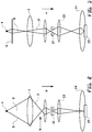
- the 1st sub-system as shown in figure 2 is arranged to form crossovers 9, 11 of multi-beams 3 in certain planes to reduce off-axis aberrations of the whole system.
- the accelerating lens 7 and condenser lens 10 focus the multi-beam in the variable aperture plane 11.
- the accelerating lens 7 is adjustable to attain different resolutions and pitches for different applications.
- Intermediate lens 13 focuses the multi-beams 3 to have a Common cross-over near the coma-free plane of objective lens 14 in order to get small aberrations.
- Aperture lens array 6 is a combination of two mechanical electrodes and an array of apertures, for example of 18 micron diameter with a 25 micron pitch, micro fabricated in a thin Si membrane. It is designed to correct for the field curvature, to have a low spherical aberration, and to nullify the chromatic deflection error.
- This lens array 6 creates an array of focused primary electron beams in the accelerator lens plane 7, with a geometrical spot size of for example 95 nm at a pitch of for example 70 micron. This ratio of spot size and pitch keeps the same on the sample.
- the objective lens 14 provides the major focusing contribution to the final spot size and aberration of the primary electron beams on the sample surface 15.
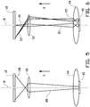
- the 3rd sub-system as shown in figure 5 is arranged to achieve the large magnification of secondary electron beams 20 by analyzing the outline of secondary electron detection system.
- the intermediate lens 13, and the objective and retarding lens 14' together project the secondary electron beams 20 with sufficient linear magnification in the detection plane of the secondary electron detector 12.
- a certain given primary beam energy determines the strength of intermediate lens 13, because in charged particle optics, the focusing condition is related to the strength of lens and the energy of electron. So in order to achieve desired magnification, or proper magnification ranges, the energy of secondary electron beam 20, or the potential difference of the electrostatic lens is limited. Proper potential difference should be optimized.
- the neighboring secondary electron beams can have large enough pitch to be separately detected by the position sensitive secondary electron detector 12 positioned substantially in the plane comprising said common cross-over of the primary electron beams 3 as shown in figure 4 .
- the 4th sub-system as shown in figure 6 provides the focusing situation of single secondary electron beams 21, 22. Under the effect of the lens system 13, 14, each single secondary electron beam 21, 22 is well focused in order to get a small enough spot size in the detection plane 12.
- the final focusing plane of the secondary electrons, the working distance and the potential difference of the retarding lens are adjustable. Unlike the focusing of the primary electrons, the final focusing plane of the secondary electrons does not have to strictly be fixed in the same position for every landing energy of the primary electrons. The final focusing plane of the secondary electrons just needs to be close to the detection plane 12 as long as it does not give rise to large secondary electron beam spread.
- the pitch of primary beams is also adjustable.
- the condenser lens 10 By using the condenser lens 10 to change the common cross-over of primary electron beams 3, the total magnification and the pitch of primary electron beams 3 can be changed.
- the sample 15 is arranged on top of a stage 30 for moving the sample surface 15 with respect to the array of primary electron beams 3.
- the movement of the stage 30 is controlled by a controller 40.
- the controller 40 also controls the scan coils 16 and, in this example, also collects the image data obtained by the CCD detector 12.
- the MBSEM When inspecting a surface of a sample 15, the MBSEM generates an array of primary electron beams 3 using a multi beam charged particle generator, wherein all primary electron beams 3 are directed to a common cross-over using a condenser lens, wherein the primary electron beams 3 are directed from the common cross-over towards the sample surface 15 and all primary electron beams 3 are focused into an array of individual spots on the sample surface 15 using a lens system 13, 14, and wherein secondary electrons which originate from the individual spots on the sample surface 15 are detected using a position sensitive secondary electron detector 12 positioned at least substantially in or near a plane comprising said common cross-over.
- the sample 15 is moved by the stage 30 in a first direction, preferably at a constant speed, while the primary electron beams 3 are scanned by the scan coils 16 repeatedly in a second direction, which second direction is at least substantially perpendicular to the first direction.
- the secondary electron beams 20, 21, 21 may move over the detection surface of the secondary electron detector 12. This movement is for example compensated by selecting the pixels for detecting one specific secondary electron beam in dependence on the settings of the deflection of the primary electron beams 3 by the scan coils 16.
- an alternative detector set-up is shown.
- the detector of this alternative detector set-up comprises a fluorescent screen 121 arranged at least substantially in or near a plane comprising said common cross-over and an optical arrangement 122, 123 for conveying photons from the fluorescent screen 121 to a CCD camera, a CMOS camera, an array of avalanche photo diodes or photo multiplier 124.
- the optical arrangement in this example comprises a mirror 122 which is provided with a through-opening for allowing the primary electron beams 3 to pass there through, and an optical lens 123 for projecting the photons from the fluorescent screen 12 onto the CCD camera 124.
- a fluorescent screen 12 is a thin disc of a YAG crystal, provided with a through opening for the primary electrons to pass there through.
- the lens system 13', 14' comprises an objective lens array 14' having an array of small objective lenses, preferably one lens for each primary electron beam 31.
- the primary electron beams 31 pass through the hole in the position sensitive secondary electron detector 12 and are in this example substantially collimated by a collimator lens 13'.
- each primary electron beam 31 is directed to its own lens in the objective lens array 14' which focuses said primary electron beam 31 on the sample surface 15.
- the secondary electron beams 32 are collected by the lenses of the objective lens array 14' and are projected onto the detecting surface of the secondary electron detector 12.
Landscapes
- Chemical & Material Sciences (AREA)
- Analytical Chemistry (AREA)
- Analysing Materials By The Use Of Radiation (AREA)
Description
- The invention relates to an apparatus and a method for inspecting a surface of a sample. In particular the invention relates to an apparatus for inspecting a sample surface using a plurality of charged particle beams, such as a multi-beam scanning electron microscope. The invention may be applied to charged particles of any type, such as electrons, positrons, ions and others.
- Such an apparatus is for example disclosed in
US patent 7,554,094 . This US patent discloses an electron microscope comprising a charged particle source for generating an array of primary electron beams. These primary electron beams pass a field lens. Downstream of this field lens, the primary electron beam path is a converging beam path having a cross-over in an intermediate plane upstream of an objective lens. The objective lens directs the primary charged particle beams from the common cross-over towards the sample surface and focuses the primary charged particle beams into an array of individual spots on the sample surface. - From the individual spots of the array of spots on the sample, secondary electrons emanate from the sample surface. In order to detect these secondary electrons, the secondary electron beam path, comprising the plurality of secondary electron beams, is separated from the primary electron beam path. To separate the secondary electron beam path from the primary electron beam path, the known apparatus comprises a beam splitter arrangement between the field lens and the cross-over. The beam splitter utilizes a magnetic field portion to deflect the primary electron beams by an angle β to the right (as viewed in the traveling direction of the primary electron beams) and to deflect the secondary electron beams by an angle γ to the right (as viewed in the traveling direction of the secondary electron beams). After the beam splitter, the separated secondary electron beams are directed towards a detector.
- A disadvantage of this system is that the use of the beam splitter as described in
US 7,554,094 deteriorates the imaging quality of the apparatus. In other words, the apparatus as described inUS 7,554,094 requires a number of additional electron-optical components to correct stigmatism, distortion and/or dispersion introduced by the magnetic field portion, in order to substantially maintain the imaging quality. Additional electron-optical components are arranged both in the primary electron beam path and in the secondary electron beam path. - From
WO2007/028596 it is known to place a detector in the cross-over plane. - It is an object of the present invention to provide a multi charged particle beam apparatus for inspecting a sample surface which provides a new detection arrangement for detecting the secondary electrons.
- According to a first aspect, the invention provides an apparatus for inspecting a surface of a sample, as described in claim 1. The apparatus comprises
a multi beam charged particle generator for generating an array of primary charged particle beams,
a condenser lens for directing all charged particle beams to a common cross-over,
a lens system for directing the primary charged particle beams from the common cross-over towards the sample surface and for focusing all primary charged particle beams into an array of individual spots on the sample surface, and
a position sensitive secondary electron detector positioned at least substantially in or near a plane comprising said common cross-over. - The invention thus provides a simple detection system in which the secondary electrons are detectable without the use of a beam splitter or Wien filter to separate the secondary charged particle beam path from the primary charged particle beam path. The disadvantages inherent with the use of such a beam splitter or Wien filter can thus be avoided.
- The invention utilizes the energy difference between the secondary electrons and the primary charged particle, for example in a SEM the energy of the primary electrons is usually from 1 keV to 30 keV and the energy of secondary electrons is usually from 0 eV to 50 eV. The result of this energy difference is that the lens system performs differently for primary charged particles than for secondary electrons. On the one hand, the lens system is arranged for focusing all primary charged particle beams into an array of individual spots on the sample surface. On the other hand, the same lens system is used for directing the secondary electron beams towards the common cross-over. Since the secondary electrons have an energy which is much less than the energy of the primary charged particles, the lens system does not necessarily focus the secondary electrons back into the common cross-over, but is preferably designed to spread the secondary electrons over an area which essentially surrounds the common cross-over. Thus, in or near a plane comprising said common cross-over, most of the secondary electron beams are spatially separated from the primary charged particle beams which are all concentrated in the common cross-over. By positioning a position sensitive secondary electron detector at least substantially in or near a plane comprising said common cross-over, preferably adjacent to and/or surrounding the common cross-over, most of the secondary electron beams can be detected without any interference to the primary charged particle beams.
- In an embodiment, the lens system is arranged for projecting the secondary electrons from the individual spots on the sample surface to individual spots on the secondary electron detector.
- In accordance with the invention, the lens system is arranged for imaging the sample surface onto the secondary electron detector using the secondary electrons. Because the secondary electrons only originate from the points in the sample surface which are hit by primary electrons, the image is an array of dots. In these embodiments, when the spatial resolution of the position sensitive secondary electron detector is chosen to be sufficiently large, the position sensitive secondary electron detector can acquire an individual secondary electron signal from most of the individual primary charged particle spots on the sample surface. Only the secondary electrons which are projected or imaged back at the position of the common cross-over cannot be detected. The secondary electrons which originated from all other spots can be detected simultaneous and separately for each spot on the sample surface. Accordingly high resolution scanning charged particle microscope images can be made n times the speed of a single beam scanning charged particle microscope, wherein n is substantially equal to the number of secondary beams that are simultaneously and separately detected by the detector. For example, n can be as large as 200, or even more.
- In an embodiment, the lens system is arranged for imaging the sample surface onto the secondary electron detector with an optical magnification in a range from 5 to 400 times. The magnification increases the pitch between individual spots of the secondary electron beams on the secondary electron detector, which makes it easier to resolve the individual secondary electron spots in the image on the secondary electron detector.
- In an embodiment, said secondary electron detector comprises a hole for passing said primary charged particle beams there-through. Preferably the primary charged particle beam path comprises an optical axis and the secondary electron detector is arranged such that the optical axis passes through the hole, preferably such that the optical axis is arranged substantially at the central axis of the hole. Preferably the secondary electron detector is arranged such that the common cross-over is in or near the hole.
- In an embodiment, the lens system comprises a magnetic objective lens. In an embodiment, the apparatus comprises a sample holder which is arranged for positioning the sample surface to be immersed in the magnetic field of the objective lens. Such an arrangement gives low aberrations for the primary electrons, which is an advantage in a microscope. Here an immersion arrangement is even more advantageous, because there must be space between the sample and a non-immersion lens to accelerate the electrons upwards, which would further increase the aberrations of the non-immersion lens. In an immersion lens the acceleration is inside the lens, which reduces aberrations. Also extracting the secondary electrons from the immersion field gives an additional possibility to set the magnification of the projection of the secondary electrons onto the secondary electron detector to a desired value.
- In an embodiment, the lens system comprises a single objective lens, preferably a single objective lens for all primary electron beams. Alternatively the lens system comprises an objective lens array having an array of small objective lenses, preferably one lens for each primary electron beam.
- In an embodiment, the apparatus comprises a field generator for providing an electrostatic field that accelerates the secondary electrons from the sample surface towards the secondary electron detector. The electrostatic field is arranged to direct the secondary electrons from the sample towards the secondary electron detector and to narrow the opening angle of the secondary electron beams. In addition the electrostatic field is used to balance the focusing requirements in the primary charged particle beams and the secondary electron beams focusing. The electrostatic field is arranged to focus the primary charged particle beams with a good resolution and to focus the secondary electron beams at the specified detection plane with sufficient magnification.
- In an embodiment in which the lens system comprises a magnetic objective lens, the field generator is arranged for providing an electrostatic field is between the sample and a pole piece of the magnetic objective lens. In an embodiment, the field generator comprises an electrostatic lens, also called a retarding lens, which is arranged below the magnetic objective lens to form an electrostatic-magnetic objective lens.
- In an embodiment, the pitch between the spots on the sample surface is between 0.3 and 30 micrometers. Preferably the pitch is less than 1 micrometer.
- In an embodiment, the detector is a CCD camera, a CMOS camera, an array of avalanche photo diodes or photo multipliers or PN junction semiconductor detectors which gets signal from secondary electrons directly.
- In an embodiment the detector comprises a fluorescent screen arranged at least substantially in or near a plane comprising said common cross-over and an optical arrangement for conveying photons from the fluorescent screen to a CCD camera, a CMOS camera, an array of avalanche photo diodes or photo multipliers. In this embodiment the CCD camera, CMOS camera, array of avalanche photo diodes or photo multipliers can be arranged at a distance from the charged particle beams.
- According to a second aspect, the invention provides a method for inspecting a surface of a sample according to
claim 13. The method comprising the steps of: - generating an array of primary charged particle beams using a multi beam charged particle generator;
- directing all charged particle beams to a common cross-over using a condenser lens;
- directing the primary charged particle beams from the common cross-over towards the sample surface and focusing all primary charged particle beams into an array of individual spots on the sample surface using a lens system; and
- detecting secondary electrons which originate from the individual spots on the sample surface using a position sensitive secondary electron detector positioned at least substantially in or near a plane comprising said common cross-over.
- In an embodiment of this method, the sample surface is moved at constant speed in a first direction while the primary charged particle beams are scanned repeatedly in a second direction at least substantially perpendicular to the first direction. This provides a new way of studying samples with a scanning charged particle beam microscope: off-line microscopy wherein a full sample surface, for example over an area of one square millimeter, is scanned and imaged at nanometer resolution after which the full sample surface is available to the specialist, for example a biologist, for studying and/or inspecting the image on a computer, instead of behind the microscope.
- In an embodiment of this method, the position sensitive secondary electron detector comprises pixels which are arranged to detect one particular secondary electron beam and to at least partially separate neighboring secondary electron beams. Preferably the secondary electron beams are at least substantially fully spatially separated on the surface of the secondary electron detector, and the size of the pixels is smaller than the spots of the secondary electron beams on the surface of the secondary electron detector. When the spots of the secondary electron beams are partially overlapping, the one particular secondary electron beam can be distinguished from its neighboring secondary electron beam by analyzing the intensity distribution in the two secondary electron beam spots and acquiring the centers and effective diameters of these spots. From such an analysis the intensity of the individual secondary electron beams can be determined.
- In an embodiment of this method, the lens system comprises a scanner for scanning the primary charged particle beams, wherein the method comprises the step of selecting the pixels for detecting one specific secondary electron beam in dependence on the settings of the scanning of the primary charged particle beams by the scanner. This provides a way of undoing a movement of the secondary electron beams on the detector due to the scanning of the primary charged particle beams on the sample surface, which can be provided by providing suitable software to control the secondary electron detector.
- The various aspects and features described and shown in the specification can be applied, individually, wherever possible. These individual aspects, in particular the aspects and features described in the attached dependent claims, can be made subject of divisional patent applications.
- The invention will be elucidated on the basis of an exemplary embodiment shown in the attached drawings, in which:
-
Figure 1 shows an example of a Multi-Beam Scanning Electron Microscope (MBSEM) of the invention, -
Figure 2 shows an envelope presentation of the primary electron beam path in the MBSEM offigure 1 , -
Figure 3 shows the beam path of one primary electron beam of the array of primary electron beams in the MBSEM offigure 1 , -
Figure 4 shows the primary electron beams in the part of the MBSEM offigure 1 from the common cross-over to the sample, -
Figure 5 shows an envelope presentation of the secondary electron beam path in the MBSEM offigure 1 , -
Figure 6 shows the beam path of a two secondary electron beams in the MBSEM offigure 1 , -
Figure 7 shows a part of the MBSEM comprising a different detector setup, and -
Figure 8 shows a part of an MBSEM comprising an array of small objective lenses. -
Figure 1 shows an example of a Multi-Beam Scanning Electron Microscope (MBSEM) of the invention. - The MBSEM 1 comprises a multi beam charged
particle generator 2 for generating an array of primary chargedparticle beams 3, in this case an array of primary electron beams 3. The multibeam electron generator 2 comprises at least oneelectron source 4 for generating a divergingelectron beam 5. The divergingelectron beam 5 is split into an array of focusedprimary electron beams 3 by anaperture lens array 6. Theprimary electron beams 3 are subsequently directed towards asample 15, as schematically indicated by the arrow P. - The multiple images of the
source 4 are positioned on the object principle plane of anaccelerator lens 7. Theaccelerator lens 7 directs theprimary electron beams 3 towards theoptical axis 8 and creates a firstcommon cross-over 9 of all the primary electron beams 3. - The first
common cross-over 9 is imaged by themagnetic condenser lens 10 onto avariable aperture 11 that acts as a current limiting aperture. At the variable aperture 11 a second common cross-over of all theprimary electron beams 3 is created. - The MBSEM comprises a
lens system variable aperture 11 towards thesample surface 15 and for focusing all primary chargedparticle beams 3 into an array of individual spots on thesample surface 15. The lens system comprises an intermediatemagnetic lens 13 for imaging thevariable aperture 11 onto a coma free plane of theobjective lens 14, whichobjective lens 14 creates an array of focused primary electron beams on thesample surface 15. - In addition the MBSEM is provided with
scan coils 16 for scanning the array of focused primary electron beams over thesample surface 15. - The MBSEM is furthermore provided with a position sensitive
secondary electron detector 12 positioned at least substantially in or near a plane comprising a common cross-over, in this case directly below thevariable aperture 11. Alternatively the position sensitivesecondary electron detector 12 can be arranged in stead of thevariable aperture 11, substantially at the position of thevariable aperture 11, as for example shown infigures 2 to 8 . This secondaryelectron detection system 12 is arranged to acquire the individual secondary electron image of each single primary electron beam spot on thesample surface 15. This means, that when thesample surface 15 is scanned in this MBSEM 1, multiple images can be acquired at the same time in one single scan period. - It is preferred that the secondary electron detection system collects most secondary electrons which are emitted over a large energy range and at a large opening angle. Besides, this secondary electron detection system should also work for a large landing energy range of the primary electrons.
- It is further preferred that the secondary electron beams are focused in the detection plane with sufficient magnification, for example a magnification in a range from 5 to 400 times. The focusing provides secondary electron beams with a small spot size on the secondary electron detector, and sufficient magnification provides a large pitch between neighboring secondary electron beams in the detection plane. In order to separate the images of different secondary electron beams, the pitch of neighboring secondary electron beams is preferably larger than the spot size of each secondary electron beam in the detection plane.
- To achieve this goal, the invention uses in-lens secondary electron detection, which will be explained in more detail below.
- Preferably the MBSEM comprises a field generator for providing an electrostatic field that accelerates the secondary electrons from the sample surface towards the
secondary electron detector 12, as indicated schematically by the arrow S. The field generator is for example arranged for providing an electrostatic field between thesample surface 15 andpole pieces 17 of the magneticobjective lens 14, as schematically shown infigure 7 . The generator is for example avoltage source 18 which provides thesample surface 15 with a negative potential with respect to thepole pieces 17. - This set-up of the
field generator 18 provides an electrostatic field which operates as an electrostatic lens (retarding lens), which is arranged between the magneticobjective lens 14 and thesample surface 15. The electrostatic lens and the magneticobjective lens 14 together form an electrostatic-magnetic objective lens. This electrostatic-magnetic objective lens accelerates the secondary electrons and narrows their opening angle. - The energy of the secondary electrons is quite small, for example in a range from 0 to 50eV with a cosine angular distribution. So the electrostatic acceleration field directs the secondary electrons in an upward direction, schematically indicated by the arrow S, with a fast velocity.
- After passing through this electrostatic lens, the opening angle α of the secondary electrons with respect to the optical axis is close to:

- Since there is a huge energy difference between energy of the secondary electrons and the energy of the primary electrons, which is usually from 1KeV to 30KeV, the focusing conditions of the
lens system same lens system - In addition, the electrostatic lens is introduced to balance the focusing requirements in the focusing of the primary and secondary electron beams. The electrostatic lens is arranged to focus the primary electrons with good resolution, and also to focus the secondary electrons at one specified detection plane with sufficient magnification.
- The most practical plane to collect the secondary electrons is the
variable aperture 11 plane, because it has smallest primary electron spot size, and it is easy to insert a position sensitive secondary electron detector at that location for practical reason. - Accordingly, the apparatus of this example comprises a position sensitive
secondary electron detector 12 positioned at least substantially in or near aplane 11 comprising said second common cross-over. - From principle analyses, this MBSEM 1 can be divided into four sub-systems, including single-source system, multi-sources system both for primary electron focusing system and secondary electron detection system. At a certain working distance and a certain landing energy, the focusing lenses make these 4 sub-systems work well.
- The 1st sub-system as shown in
figure 2 is arranged to formcrossovers multi-beams 3 in certain planes to reduce off-axis aberrations of the whole system. The acceleratinglens 7 andcondenser lens 10 focus the multi-beam in thevariable aperture plane 11. The acceleratinglens 7 is adjustable to attain different resolutions and pitches for different applications.Intermediate lens 13 focuses the multi-beams 3 to have a Common cross-over near the coma-free plane ofobjective lens 14 in order to get small aberrations. - The 2nd sub-system as shown in
figure 3 is arranged to focus each single primary electron beam 3' with good resolution.Aperture lens array 6 is a combination of two mechanical electrodes and an array of apertures, for example of 18 micron diameter with a 25 micron pitch, micro fabricated in a thin Si membrane. It is designed to correct for the field curvature, to have a low spherical aberration, and to nullify the chromatic deflection error. Thislens array 6 creates an array of focused primary electron beams in theaccelerator lens plane 7, with a geometrical spot size of for example 95 nm at a pitch of for example 70 micron. This ratio of spot size and pitch keeps the same on the sample. Theobjective lens 14 provides the major focusing contribution to the final spot size and aberration of the primary electron beams on thesample surface 15. - The 3rd sub-system as shown in
figure 5 is arranged to achieve the large magnification ofsecondary electron beams 20 by analyzing the outline of secondary electron detection system. Theintermediate lens 13, and the objective and retarding lens 14' together project thesecondary electron beams 20 with sufficient linear magnification in the detection plane of thesecondary electron detector 12. A certain given primary beam energy determines the strength ofintermediate lens 13, because in charged particle optics, the focusing condition is related to the strength of lens and the energy of electron. So in order to achieve desired magnification, or proper magnification ranges, the energy ofsecondary electron beam 20, or the potential difference of the electrostatic lens is limited. Proper potential difference should be optimized. After selecting a good potential difference and proper settings oflenses secondary electron detector 12 positioned substantially in the plane comprising said common cross-over of theprimary electron beams 3 as shown infigure 4 . - The 4th sub-system as shown in
figure 6 provides the focusing situation of singlesecondary electron beams lens system secondary electron beam detection plane 12. - At one landing energy of the primary electron beams on the
sample surface 15, the final focusing plane of the secondary electrons, the working distance and the potential difference of the retarding lens are adjustable. Unlike the focusing of the primary electrons, the final focusing plane of the secondary electrons does not have to strictly be fixed in the same position for every landing energy of the primary electrons. The final focusing plane of the secondary electrons just needs to be close to thedetection plane 12 as long as it does not give rise to large secondary electron beam spread. - Besides, the pitch of primary beams is also adjustable. By using the
condenser lens 10 to change the common cross-over ofprimary electron beams 3, the total magnification and the pitch ofprimary electron beams 3 can be changed. - As schematically shown in
figure 4 , thesample 15 is arranged on top of astage 30 for moving thesample surface 15 with respect to the array of primary electron beams 3. The movement of thestage 30 is controlled by acontroller 40. Thecontroller 40 also controls the scan coils 16 and, in this example, also collects the image data obtained by theCCD detector 12. - When inspecting a surface of a
sample 15, the MBSEM generates an array ofprimary electron beams 3 using a multi beam charged particle generator, wherein allprimary electron beams 3 are directed to a common cross-over using a condenser lens, wherein theprimary electron beams 3 are directed from the common cross-over towards thesample surface 15 and allprimary electron beams 3 are focused into an array of individual spots on thesample surface 15 using alens system sample surface 15 are detected using a position sensitivesecondary electron detector 12 positioned at least substantially in or near a plane comprising said common cross-over. - In order to obtain an image of a large surface, in one exemplary embodiment, the
sample 15 is moved by thestage 30 in a first direction, preferably at a constant speed, while theprimary electron beams 3 are scanned by the scan coils 16 repeatedly in a second direction, which second direction is at least substantially perpendicular to the first direction. - When the
primary electron beams 3 are scanned over thesample surface 15, thesecondary electron beams secondary electron detector 12. This movement is for example compensated by selecting the pixels for detecting one specific secondary electron beam in dependence on the settings of the deflection of theprimary electron beams 3 by the scan coils 16. - In
figure 7 , an alternative detector set-up is shown. In stead of using adetector 12 which gives a signal when hit directly bysecondary electrons particle beam 3 path as discussed in the previous examples, the detector of this alternative detector set-up comprises afluorescent screen 121 arranged at least substantially in or near a plane comprising said common cross-over and anoptical arrangement fluorescent screen 121 to a CCD camera, a CMOS camera, an array of avalanche photo diodes orphoto multiplier 124. The optical arrangement in this example comprises amirror 122 which is provided with a through-opening for allowing theprimary electron beams 3 to pass there through, and anoptical lens 123 for projecting the photons from thefluorescent screen 12 onto theCCD camera 124. An example of such afluorescent screen 12 is a thin disc of a YAG crystal, provided with a through opening for the primary electrons to pass there through. - In
figure 8 , an alternative of thesingle lens objective 14 is shown. In the alternative set-up, the lens system 13', 14' comprises an objective lens array 14' having an array of small objective lenses, preferably one lens for eachprimary electron beam 31. As schematically shown, theprimary electron beams 31 pass through the hole in the position sensitivesecondary electron detector 12 and are in this example substantially collimated by a collimator lens 13'. Subsequently eachprimary electron beam 31 is directed to its own lens in the objective lens array 14' which focuses saidprimary electron beam 31 on thesample surface 15. Thesecondary electron beams 32 are collected by the lenses of the objective lens array 14' and are projected onto the detecting surface of thesecondary electron detector 12. - It is to be understood that the above description is included to illustrate the operation of the preferred embodiments and is not meant to limit the scope of the invention. From the above discussion, many variations will be apparent to one skilled in the art that would yet be encompassed by the scope of the attached claims.
Claims (15)
- An apparatus for inspecting a surface of a sample (15), wherein the apparatus comprises
a multi beam charged particle generator for generating an array of primary charged particle beams (3),
a condenser lens (10) for directing all charged particle beams to a common cross-over,
a lens system (13, 14) for directing the primary charged particle beams from the common cross-over towards the sample surface and for focusing all primary charged particle beams into an array of individual spots on the sample surface,
a secondary electron detector positioned at least substantially in or near the plane comprising said common cross-over,
characterized in that the lens system is arranged for imaging the sample surface onto the secondary electron detector using secondary electrons, and in that the secondary electron detector is a position sensitive secondary electron detector (12). - Apparatus according to claim 1, wherein the lens system is arranged for projecting the secondary electrons from an individual spot on the sample surface to an individual spot on the secondary electron detector.
- Apparatus according to claim 2, wherein the lens system is arranged for imaging the sample surface onto the secondary electron detector with an optical magnification in a range from 5 to 400 times.
- Apparatus according to any one of the previous claims, wherein said secondary electron detector comprises a hole for passing said primary charged particle beams there-through.
- Apparatus according to any one of the previous claims, wherein the lens system comprises a magnetic objective lens, preferably wherein the apparatus comprises a sample holder which is arranged for positioning the sample surface to be immersed in the magnetic field of the objective lens.
- Apparatus according to any one of the previous claims, wherein the lens system comprises a single objective lens.
- Apparatus according to any one of the claims 1 to 5, wherein the lens system comprises an objective lens array having an array of small objective lenses, preferably one lens for each primary electron beam.
- Apparatus according to any one of the previous claims, wherein the apparatus comprises a field generator for providing an electrostatic field that accelerates the secondary electrons from the sample surface towards the secondary electron detector.
- Apparatus according to claim 8, when dependent of claim 5, wherein the field generator is arranged for providing an electrostatic field between the sample and a pole piece of the magnetic objective lens.
- Apparatus according to any one of the previous claims, wherein the pitch between the spots on the sample surface is between 0.3 and 30 micrometers.
- Apparatus according to any one of the previous claims, wherein the detector is a CCD camera, a CMOS camera, an array of avalanche photo diodes, photo multipliers or PN junction semiconductor detector which gets signal from secondary electrons directly.
- Apparatus according to any one of the claims 1 to 10, wherein the detector comprises a fluorescent screen arranged at least substantially in or near the plane comprising said common cross-over and an optical arrangement for conveying photons from the fluorescent screen to a CCD camera, a CMOS camera, an array of avalanche photo diodes or photo multiplier.
- Method for inspecting a surface of a sample comprising the steps of:generating an array of primary charged particle beams using a multi beam charged particle generator;directing all charged particle beams to a common cross-over using a condenser lens;directing the primary charged particle beams from the common cross-over towards the sample surface and focusing all primary charged particle beams into an array of individual spots on the sample surface using a lens system;detecting secondary electrons which originate from the individual spots on the sample surface using a position sensitive secondary electron detector positioned at least substantially in or near a plane comprising said common cross-over;wherein the lens system is arranged for imaging the sample surface onto the secondary electron detector using the secondary electrons.
- Method according to claim 13, in which the sample surface is moved at constant speed in a first direction while the primary charged particle beams are scanned repeatedly in a second direction at least substantially perpendicular to the first direction.
- Method according to claim 14, in which the lens system comprises a scanner for scanning the primary charged particle beams, wherein the method comprises the step of selecting the pixels for detecting one specific secondary electron beam in dependence on the settings of the scanning of the primary charged particle beams by the scanner.
Applications Claiming Priority (2)
| Application Number | Priority Date | Filing Date | Title |
|---|---|---|---|
| NL2009053A NL2009053C2 (en) | 2012-06-22 | 2012-06-22 | Apparatus and method for inspecting a surface of a sample. |
| PCT/NL2013/050416 WO2013191539A1 (en) | 2012-06-22 | 2013-06-12 | Apparatus and method for inspecting a surface of a sample |
Publications (2)
| Publication Number | Publication Date |
|---|---|
| EP2864997A1 EP2864997A1 (en) | 2015-04-29 |
| EP2864997B1 true EP2864997B1 (en) | 2017-01-18 |
Family
ID=46881131
Family Applications (1)
| Application Number | Title | Priority Date | Filing Date |
|---|---|---|---|
| EP13733082.5A Active EP2864997B1 (en) | 2012-06-22 | 2013-06-12 | Apparatus and method for inspecting a surface of a sample |
Country Status (8)
| Country | Link |
|---|---|
| US (1) | US9697985B2 (en) |
| EP (1) | EP2864997B1 (en) |
| JP (1) | JP6268169B2 (en) |
| KR (1) | KR20150035741A (en) |
| CN (1) | CN104488064B (en) |
| IL (1) | IL236320A0 (en) |
| NL (1) | NL2009053C2 (en) |
| WO (1) | WO2013191539A1 (en) |
Cited By (2)
| Publication number | Priority date | Publication date | Assignee | Title |
|---|---|---|---|---|
| EP3703100A1 (en) | 2019-02-27 | 2020-09-02 | FEI Company | Charged particle beam device for inspection of a specimen with a plurality of charged particle beamlets |
| EP3882951A1 (en) | 2020-03-19 | 2021-09-22 | FEI Company | Charged particle beam device for inspection of a specimen with a plurality of charged particle beamlets |
Families Citing this family (23)
| Publication number | Priority date | Publication date | Assignee | Title |
|---|---|---|---|---|
| US10903042B2 (en) | 2014-05-08 | 2021-01-26 | Technische Universiteit Delft | Apparatus and method for inspecting a sample using a plurality of charged particle beams |
| NL2012780B1 (en) | 2014-05-08 | 2016-02-23 | Univ Delft Tech | Apparatus and method for inspecting a sample using a plurality of charged particle beams. |
| NL2013411B1 (en) * | 2014-09-04 | 2016-09-27 | Univ Delft Tech | Multi electron beam inspection apparatus. |
| US9966224B2 (en) * | 2014-10-22 | 2018-05-08 | Sciencetomorrow Llc | Quantitative secondary electron detection |
| JP2016115680A (en) * | 2014-12-17 | 2016-06-23 | アプライド マテリアルズ イスラエル リミテッド | Scanning charged particle beam device having aberration correction aperture and operation method thereof |
| US10192716B2 (en) | 2015-09-21 | 2019-01-29 | Kla-Tencor Corporation | Multi-beam dark field imaging |
| US10460905B2 (en) | 2015-09-23 | 2019-10-29 | Kla-Tencor Corporation | Backscattered electrons (BSE) imaging using multi-beam tools |
| US10062541B2 (en) * | 2016-01-27 | 2018-08-28 | Hermes Microvision Inc. | Apparatus of plural charged-particle beams |
| JP6742015B2 (en) * | 2016-01-29 | 2020-08-19 | 株式会社ホロン | Electronic detection device and electronic detection method |
| US10453645B2 (en) * | 2016-12-01 | 2019-10-22 | Applied Materials Israel Ltd. | Method for inspecting a specimen and charged particle multi-beam device |
| TWI729368B (en) * | 2017-02-08 | 2021-06-01 | 荷蘭商Asml荷蘭公司 | Source-conversion unit, multi-beam apparatus and method to configure a multi-beam apparatus |
| TWI787802B (en) * | 2017-02-08 | 2022-12-21 | 荷蘭商Asml荷蘭公司 | Source-conversion unit, multi-beam apparatus and method to configure a multi-beam apparatus |
| TWI658487B (en) * | 2017-02-08 | 2019-05-01 | 荷蘭商Asml荷蘭公司 | Multi-beam apparatus and method for observing a sample surface |
| US10176965B1 (en) | 2017-07-05 | 2019-01-08 | ICT Integrated Circuit Testing Gesellschaft für Halbleiterprüftechnik mbH | Aberration-corrected multibeam source, charged particle beam device and method of imaging or illuminating a specimen with an array of primary charged particle beamlets |
| JP2019164886A (en) | 2018-03-19 | 2019-09-26 | 株式会社日立ハイテクノロジーズ | Beam irradiation device |
| JP7085258B2 (en) * | 2018-04-13 | 2022-06-16 | 株式会社ホロン | Ultra-high-speed electron detector and scanning electron beam inspection device incorporating the detector |
| EP3716312A1 (en) | 2019-03-28 | 2020-09-30 | FEI Company | Charged particle beam device for inspection of a specimen with a plurality of charged particle beamlets |
| NL2024606B1 (en) | 2020-01-06 | 2021-09-07 | Delmic Ip B V | Method and apparatus for inspecting a sample by means of multiple charged particle beamlets |
| EP3869533A1 (en) * | 2020-02-21 | 2021-08-25 | ASML Netherlands B.V. | Charged particle assessment tool, inspection method |
| EP4009349A1 (en) * | 2020-12-03 | 2022-06-08 | ASML Netherlands B.V. | Charged particle tool, calibration method, inspection method |
| CN113035675A (en) * | 2021-02-26 | 2021-06-25 | 中国科学院生物物理研究所 | Charged particle beam apparatus |
| TW202312205A (en) | 2021-05-27 | 2023-03-16 | 德商卡爾蔡司多重掃描電子顯微鏡有限公司 | Multi-beam charged particle system and method of controlling the working distance in a multi-beam charged particle system |
| EP4131329A1 (en) * | 2021-08-02 | 2023-02-08 | ASML Netherlands B.V. | Charged-particle optical device |
Family Cites Families (13)
| Publication number | Priority date | Publication date | Assignee | Title |
|---|---|---|---|---|
| EP1150327B1 (en) * | 2000-04-27 | 2018-02-14 | ICT, Integrated Circuit Testing Gesellschaft für Halbleiterprüftechnik mbH | Multi beam charged particle device |
| JPWO2002056332A1 (en) * | 2001-01-10 | 2004-05-20 | 株式会社荏原製作所 | Inspection apparatus using electron beam, inspection method, and device manufacturing method using the inspection apparatus |
| DE60236302D1 (en) * | 2002-12-17 | 2010-06-17 | Integrated Circuit Testing | Multi-axis compound lens, blasting device and method of using this combined lens |
| EP2579268A1 (en) | 2003-09-05 | 2013-04-10 | Carl Zeiss SMT GmbH | Particle-optical systems and arrangements and particle-optical components for such systems and arrangements |
| JP4987486B2 (en) | 2005-01-07 | 2012-07-25 | エスアイアイ・ナノテクノロジー株式会社 | Thin film sample measurement method and apparatus, and thin film sample preparation method and apparatus |
| US8039813B2 (en) * | 2005-09-06 | 2011-10-18 | Carl Zeiss Smt Gmbh | Charged particle-optical systems, methods and components |
| JP4878501B2 (en) | 2006-05-25 | 2012-02-15 | 株式会社日立ハイテクノロジーズ | Charged particle beam application equipment |
| JP5101845B2 (en) | 2006-08-21 | 2012-12-19 | エスアイアイ・ナノテクノロジー株式会社 | Focused ion beam apparatus, sample cross section preparation method and thin piece sample preparation method using the same |
| US7851755B2 (en) * | 2006-12-20 | 2010-12-14 | Jeol Ltd. | Apparatus for detecting backscattered electrons in a beam apparatus |
| WO2008101713A2 (en) * | 2007-02-22 | 2008-08-28 | Applied Materials Israel Ltd. | High throughput sem tool |
| EP2219204B1 (en) * | 2009-02-12 | 2012-03-21 | ICT, Integrated Circuit Testing Gesellschaft für Halbleiterprüftechnik mbH | Arrangement and method for the contrast improvement in a charged particle beam device for inspecting a specimen |
| JP5749028B2 (en) * | 2011-02-11 | 2015-07-15 | 株式会社ホロン | Scanning electron microscope |
| US8362425B2 (en) * | 2011-03-23 | 2013-01-29 | Kla-Tencor Corporation | Multiple-beam system for high-speed electron-beam inspection |
-
2012
- 2012-06-22 NL NL2009053A patent/NL2009053C2/en not_active IP Right Cessation
-
2013
- 2013-06-12 EP EP13733082.5A patent/EP2864997B1/en active Active
- 2013-06-12 WO PCT/NL2013/050416 patent/WO2013191539A1/en not_active Ceased
- 2013-06-12 KR KR1020147036175A patent/KR20150035741A/en not_active Withdrawn
- 2013-06-12 JP JP2015518354A patent/JP6268169B2/en active Active
- 2013-06-12 CN CN201380031526.XA patent/CN104488064B/en active Active
- 2013-06-12 US US14/408,137 patent/US9697985B2/en active Active
-
2014
- 2014-12-17 IL IL236320A patent/IL236320A0/en unknown
Non-Patent Citations (1)
| Title |
|---|
| None * |
Cited By (3)
| Publication number | Priority date | Publication date | Assignee | Title |
|---|---|---|---|---|
| EP3703100A1 (en) | 2019-02-27 | 2020-09-02 | FEI Company | Charged particle beam device for inspection of a specimen with a plurality of charged particle beamlets |
| EP3828914A1 (en) | 2019-02-27 | 2021-06-02 | FEI Company | Charged particle beam device for inspection of a specimen with a plurality of charged particle beamlets |
| EP3882951A1 (en) | 2020-03-19 | 2021-09-22 | FEI Company | Charged particle beam device for inspection of a specimen with a plurality of charged particle beamlets |
Also Published As
| Publication number | Publication date |
|---|---|
| EP2864997A1 (en) | 2015-04-29 |
| KR20150035741A (en) | 2015-04-07 |
| CN104488064A (en) | 2015-04-01 |
| JP6268169B2 (en) | 2018-01-24 |
| US9697985B2 (en) | 2017-07-04 |
| US20150179399A1 (en) | 2015-06-25 |
| CN104488064B (en) | 2017-09-29 |
| IL236320A0 (en) | 2015-02-26 |
| JP2015520501A (en) | 2015-07-16 |
| NL2009053C2 (en) | 2013-12-24 |
| WO2013191539A1 (en) | 2013-12-27 |
Similar Documents
| Publication | Publication Date | Title |
|---|---|---|
| US9697985B2 (en) | Apparatus and method for inspecting a surface of a sample | |
| US11562881B2 (en) | Charged particle beam system | |
| US11239053B2 (en) | Charged particle beam system and method | |
| JP6728498B2 (en) | Method for inspecting a test piece and charged particle multi-beam apparatus | |
| US11217423B2 (en) | Apparatus of plural charged-particle beams | |
| US9449789B2 (en) | Apparatus and method for inspecting a surface of a sample | |
| US9922796B1 (en) | Method for inspecting a specimen and charged particle multi-beam device | |
| US9035249B1 (en) | Multi-beam system for high throughput EBI | |
| KR102207766B1 (en) | Secondary electron optics & detection device | |
| TWI743262B (en) | System for aberration correction in an electron beam system | |
| EP3924994B1 (en) | Device and method for operating a charged particle device with multiple beamlets | |
| US9595417B2 (en) | High resolution charged particle beam device and method of operating the same | |
| US20250349500A1 (en) | Multi-beam charged particle microscope design with a detection unit for fast compensation of charging effects | |
| JP7188910B2 (en) | Particle source and particle-optical device for generating a particle beam | |
| JP2026009673A (en) | Image generating device and image generating method |
Legal Events
| Date | Code | Title | Description |
|---|---|---|---|
| PUAI | Public reference made under article 153(3) epc to a published international application that has entered the european phase |
Free format text: ORIGINAL CODE: 0009012 |
|
| 17P | Request for examination filed |
Effective date: 20141203 |
|
| AK | Designated contracting states |
Kind code of ref document: A1 Designated state(s): AL AT BE BG CH CY CZ DE DK EE ES FI FR GB GR HR HU IE IS IT LI LT LU LV MC MK MT NL NO PL PT RO RS SE SI SK SM TR |
|
| AX | Request for extension of the european patent |
Extension state: BA ME |
|
| DAX | Request for extension of the european patent (deleted) | ||
| GRAP | Despatch of communication of intention to grant a patent |
Free format text: ORIGINAL CODE: EPIDOSNIGR1 |
|
| INTG | Intention to grant announced |
Effective date: 20160324 |
|
| GRAJ | Information related to disapproval of communication of intention to grant by the applicant or resumption of examination proceedings by the epo deleted |
Free format text: ORIGINAL CODE: EPIDOSDIGR1 |
|
| GRAP | Despatch of communication of intention to grant a patent |
Free format text: ORIGINAL CODE: EPIDOSNIGR1 |
|
| INTC | Intention to grant announced (deleted) | ||
| INTG | Intention to grant announced |
Effective date: 20160810 |
|
| GRAS | Grant fee paid |
Free format text: ORIGINAL CODE: EPIDOSNIGR3 |
|
| GRAA | (expected) grant |
Free format text: ORIGINAL CODE: 0009210 |
|
| AK | Designated contracting states |
Kind code of ref document: B1 Designated state(s): AL AT BE BG CH CY CZ DE DK EE ES FI FR GB GR HR HU IE IS IT LI LT LU LV MC MK MT NL NO PL PT RO RS SE SI SK SM TR |
|
| REG | Reference to a national code |
Ref country code: GB Ref legal event code: FG4D |
|
| REG | Reference to a national code |
Ref country code: CH Ref legal event code: EP |
|
| REG | Reference to a national code |
Ref country code: AT Ref legal event code: REF Ref document number: 863338 Country of ref document: AT Kind code of ref document: T Effective date: 20170215 |
|
| REG | Reference to a national code |
Ref country code: IE Ref legal event code: FG4D |
|
| REG | Reference to a national code |
Ref country code: DE Ref legal event code: R096 Ref document number: 602013016725 Country of ref document: DE |
|
| REG | Reference to a national code |
Ref country code: NL Ref legal event code: FP |
|
| REG | Reference to a national code |
Ref country code: LT Ref legal event code: MG4D |
|
| REG | Reference to a national code |
Ref country code: AT Ref legal event code: MK05 Ref document number: 863338 Country of ref document: AT Kind code of ref document: T Effective date: 20170118 |
|
| REG | Reference to a national code |
Ref country code: FR Ref legal event code: PLFP Year of fee payment: 5 |
|
| PG25 | Lapsed in a contracting state [announced via postgrant information from national office to epo] |
Ref country code: HR Free format text: LAPSE BECAUSE OF FAILURE TO SUBMIT A TRANSLATION OF THE DESCRIPTION OR TO PAY THE FEE WITHIN THE PRESCRIBED TIME-LIMIT Effective date: 20170118 Ref country code: IS Free format text: LAPSE BECAUSE OF FAILURE TO SUBMIT A TRANSLATION OF THE DESCRIPTION OR TO PAY THE FEE WITHIN THE PRESCRIBED TIME-LIMIT Effective date: 20170518 Ref country code: LT Free format text: LAPSE BECAUSE OF FAILURE TO SUBMIT A TRANSLATION OF THE DESCRIPTION OR TO PAY THE FEE WITHIN THE PRESCRIBED TIME-LIMIT Effective date: 20170118 Ref country code: GR Free format text: LAPSE BECAUSE OF FAILURE TO SUBMIT A TRANSLATION OF THE DESCRIPTION OR TO PAY THE FEE WITHIN THE PRESCRIBED TIME-LIMIT Effective date: 20170419 Ref country code: NO Free format text: LAPSE BECAUSE OF FAILURE TO SUBMIT A TRANSLATION OF THE DESCRIPTION OR TO PAY THE FEE WITHIN THE PRESCRIBED TIME-LIMIT Effective date: 20170418 Ref country code: FI Free format text: LAPSE BECAUSE OF FAILURE TO SUBMIT A TRANSLATION OF THE DESCRIPTION OR TO PAY THE FEE WITHIN THE PRESCRIBED TIME-LIMIT Effective date: 20170118 |
|
| PG25 | Lapsed in a contracting state [announced via postgrant information from national office to epo] |
Ref country code: PL Free format text: LAPSE BECAUSE OF FAILURE TO SUBMIT A TRANSLATION OF THE DESCRIPTION OR TO PAY THE FEE WITHIN THE PRESCRIBED TIME-LIMIT Effective date: 20170118 Ref country code: SE Free format text: LAPSE BECAUSE OF FAILURE TO SUBMIT A TRANSLATION OF THE DESCRIPTION OR TO PAY THE FEE WITHIN THE PRESCRIBED TIME-LIMIT Effective date: 20170118 Ref country code: LV Free format text: LAPSE BECAUSE OF FAILURE TO SUBMIT A TRANSLATION OF THE DESCRIPTION OR TO PAY THE FEE WITHIN THE PRESCRIBED TIME-LIMIT Effective date: 20170118 Ref country code: PT Free format text: LAPSE BECAUSE OF FAILURE TO SUBMIT A TRANSLATION OF THE DESCRIPTION OR TO PAY THE FEE WITHIN THE PRESCRIBED TIME-LIMIT Effective date: 20170518 Ref country code: RS Free format text: LAPSE BECAUSE OF FAILURE TO SUBMIT A TRANSLATION OF THE DESCRIPTION OR TO PAY THE FEE WITHIN THE PRESCRIBED TIME-LIMIT Effective date: 20170118 Ref country code: AT Free format text: LAPSE BECAUSE OF FAILURE TO SUBMIT A TRANSLATION OF THE DESCRIPTION OR TO PAY THE FEE WITHIN THE PRESCRIBED TIME-LIMIT Effective date: 20170118 Ref country code: ES Free format text: LAPSE BECAUSE OF FAILURE TO SUBMIT A TRANSLATION OF THE DESCRIPTION OR TO PAY THE FEE WITHIN THE PRESCRIBED TIME-LIMIT Effective date: 20170118 Ref country code: BG Free format text: LAPSE BECAUSE OF FAILURE TO SUBMIT A TRANSLATION OF THE DESCRIPTION OR TO PAY THE FEE WITHIN THE PRESCRIBED TIME-LIMIT Effective date: 20170418 |
|
| REG | Reference to a national code |
Ref country code: DE Ref legal event code: R097 Ref document number: 602013016725 Country of ref document: DE |
|
| PG25 | Lapsed in a contracting state [announced via postgrant information from national office to epo] |
Ref country code: SK Free format text: LAPSE BECAUSE OF FAILURE TO SUBMIT A TRANSLATION OF THE DESCRIPTION OR TO PAY THE FEE WITHIN THE PRESCRIBED TIME-LIMIT Effective date: 20170118 Ref country code: EE Free format text: LAPSE BECAUSE OF FAILURE TO SUBMIT A TRANSLATION OF THE DESCRIPTION OR TO PAY THE FEE WITHIN THE PRESCRIBED TIME-LIMIT Effective date: 20170118 Ref country code: RO Free format text: LAPSE BECAUSE OF FAILURE TO SUBMIT A TRANSLATION OF THE DESCRIPTION OR TO PAY THE FEE WITHIN THE PRESCRIBED TIME-LIMIT Effective date: 20170118 Ref country code: CZ Free format text: LAPSE BECAUSE OF FAILURE TO SUBMIT A TRANSLATION OF THE DESCRIPTION OR TO PAY THE FEE WITHIN THE PRESCRIBED TIME-LIMIT Effective date: 20170118 Ref country code: IT Free format text: LAPSE BECAUSE OF FAILURE TO SUBMIT A TRANSLATION OF THE DESCRIPTION OR TO PAY THE FEE WITHIN THE PRESCRIBED TIME-LIMIT Effective date: 20170118 |
|
| PLBE | No opposition filed within time limit |
Free format text: ORIGINAL CODE: 0009261 |
|
| STAA | Information on the status of an ep patent application or granted ep patent |
Free format text: STATUS: NO OPPOSITION FILED WITHIN TIME LIMIT |
|
| PG25 | Lapsed in a contracting state [announced via postgrant information from national office to epo] |
Ref country code: DK Free format text: LAPSE BECAUSE OF FAILURE TO SUBMIT A TRANSLATION OF THE DESCRIPTION OR TO PAY THE FEE WITHIN THE PRESCRIBED TIME-LIMIT Effective date: 20170118 Ref country code: SM Free format text: LAPSE BECAUSE OF FAILURE TO SUBMIT A TRANSLATION OF THE DESCRIPTION OR TO PAY THE FEE WITHIN THE PRESCRIBED TIME-LIMIT Effective date: 20170118 |
|
| 26N | No opposition filed |
Effective date: 20171019 |
|
| PG25 | Lapsed in a contracting state [announced via postgrant information from national office to epo] |
Ref country code: MC Free format text: LAPSE BECAUSE OF FAILURE TO SUBMIT A TRANSLATION OF THE DESCRIPTION OR TO PAY THE FEE WITHIN THE PRESCRIBED TIME-LIMIT Effective date: 20170118 |
|
| REG | Reference to a national code |
Ref country code: CH Ref legal event code: PL |
|
| PG25 | Lapsed in a contracting state [announced via postgrant information from national office to epo] |
Ref country code: SI Free format text: LAPSE BECAUSE OF FAILURE TO SUBMIT A TRANSLATION OF THE DESCRIPTION OR TO PAY THE FEE WITHIN THE PRESCRIBED TIME-LIMIT Effective date: 20170118 |
|
| REG | Reference to a national code |
Ref country code: IE Ref legal event code: MM4A |
|
| PG25 | Lapsed in a contracting state [announced via postgrant information from national office to epo] |
Ref country code: CH Free format text: LAPSE BECAUSE OF NON-PAYMENT OF DUE FEES Effective date: 20170630 Ref country code: LI Free format text: LAPSE BECAUSE OF NON-PAYMENT OF DUE FEES Effective date: 20170630 Ref country code: LU Free format text: LAPSE BECAUSE OF NON-PAYMENT OF DUE FEES Effective date: 20170612 Ref country code: IE Free format text: LAPSE BECAUSE OF NON-PAYMENT OF DUE FEES Effective date: 20170612 |
|
| REG | Reference to a national code |
Ref country code: BE Ref legal event code: MM Effective date: 20170630 |
|
| REG | Reference to a national code |
Ref country code: FR Ref legal event code: PLFP Year of fee payment: 6 |
|
| PG25 | Lapsed in a contracting state [announced via postgrant information from national office to epo] |
Ref country code: BE Free format text: LAPSE BECAUSE OF NON-PAYMENT OF DUE FEES Effective date: 20170630 |
|
| PGFP | Annual fee paid to national office [announced via postgrant information from national office to epo] |
Ref country code: FR Payment date: 20180605 Year of fee payment: 6 |
|
| PG25 | Lapsed in a contracting state [announced via postgrant information from national office to epo] |
Ref country code: MT Free format text: LAPSE BECAUSE OF NON-PAYMENT OF DUE FEES Effective date: 20170612 |
|
| PGFP | Annual fee paid to national office [announced via postgrant information from national office to epo] |
Ref country code: GB Payment date: 20180522 Year of fee payment: 6 |
|
| PG25 | Lapsed in a contracting state [announced via postgrant information from national office to epo] |
Ref country code: HU Free format text: LAPSE BECAUSE OF FAILURE TO SUBMIT A TRANSLATION OF THE DESCRIPTION OR TO PAY THE FEE WITHIN THE PRESCRIBED TIME-LIMIT; INVALID AB INITIO Effective date: 20130612 |
|
| PG25 | Lapsed in a contracting state [announced via postgrant information from national office to epo] |
Ref country code: CY Free format text: LAPSE BECAUSE OF FAILURE TO SUBMIT A TRANSLATION OF THE DESCRIPTION OR TO PAY THE FEE WITHIN THE PRESCRIBED TIME-LIMIT Effective date: 20170118 |
|
| PG25 | Lapsed in a contracting state [announced via postgrant information from national office to epo] |
Ref country code: MK Free format text: LAPSE BECAUSE OF FAILURE TO SUBMIT A TRANSLATION OF THE DESCRIPTION OR TO PAY THE FEE WITHIN THE PRESCRIBED TIME-LIMIT Effective date: 20170118 |
|
| GBPC | Gb: european patent ceased through non-payment of renewal fee |
Effective date: 20190612 |
|
| PG25 | Lapsed in a contracting state [announced via postgrant information from national office to epo] |
Ref country code: TR Free format text: LAPSE BECAUSE OF FAILURE TO SUBMIT A TRANSLATION OF THE DESCRIPTION OR TO PAY THE FEE WITHIN THE PRESCRIBED TIME-LIMIT Effective date: 20170118 |
|
| PG25 | Lapsed in a contracting state [announced via postgrant information from national office to epo] |
Ref country code: GB Free format text: LAPSE BECAUSE OF NON-PAYMENT OF DUE FEES Effective date: 20190612 |
|
| PG25 | Lapsed in a contracting state [announced via postgrant information from national office to epo] |
Ref country code: FR Free format text: LAPSE BECAUSE OF NON-PAYMENT OF DUE FEES Effective date: 20190630 |
|
| PG25 | Lapsed in a contracting state [announced via postgrant information from national office to epo] |
Ref country code: AL Free format text: LAPSE BECAUSE OF FAILURE TO SUBMIT A TRANSLATION OF THE DESCRIPTION OR TO PAY THE FEE WITHIN THE PRESCRIBED TIME-LIMIT Effective date: 20170118 |
|
| P01 | Opt-out of the competence of the unified patent court (upc) registered |
Effective date: 20230517 |
|
| PGFP | Annual fee paid to national office [announced via postgrant information from national office to epo] |
Ref country code: DE Payment date: 20260623 Year of fee payment: 14 |
|
| PGFP | Annual fee paid to national office [announced via postgrant information from national office to epo] |
Ref country code: NL Payment date: 20260622 Year of fee payment: 14 |