EP2863526A1 - Switched mode power supply peak-efficiency detection - Google Patents
Switched mode power supply peak-efficiency detection Download PDFInfo
- Publication number
- EP2863526A1 EP2863526A1 EP20130306449 EP13306449A EP2863526A1 EP 2863526 A1 EP2863526 A1 EP 2863526A1 EP 20130306449 EP20130306449 EP 20130306449 EP 13306449 A EP13306449 A EP 13306449A EP 2863526 A1 EP2863526 A1 EP 2863526A1
- Authority
- EP
- European Patent Office
- Prior art keywords
- module
- sps
- signal
- losses
- cmd
- Prior art date
- Legal status (The legal status is an assumption and is not a legal conclusion. Google has not performed a legal analysis and makes no representation as to the accuracy of the status listed.)
- Ceased
Links
- 238000001514 detection method Methods 0.000 title claims abstract description 13
- 239000003990 capacitor Substances 0.000 claims description 33
- 238000000034 method Methods 0.000 claims description 14
- 238000004891 communication Methods 0.000 claims description 5
- 230000003213 activating effect Effects 0.000 claims description 4
- 239000002184 metal Substances 0.000 claims description 3
- 239000004065 semiconductor Substances 0.000 claims description 3
- 238000010586 diagram Methods 0.000 description 9
- 230000003071 parasitic effect Effects 0.000 description 8
- 230000000873 masking effect Effects 0.000 description 6
- 230000010354 integration Effects 0.000 description 5
- 238000004088 simulation Methods 0.000 description 4
- 101100247669 Quaranfil virus (isolate QrfV/Tick/Afghanistan/EG_T_377/1968) PB1 gene Proteins 0.000 description 3
- 101150025928 Segment-1 gene Proteins 0.000 description 3
- 101100242902 Thogoto virus (isolate SiAr 126) Segment 1 gene Proteins 0.000 description 3
- 238000013459 approach Methods 0.000 description 3
- 230000001413 cellular effect Effects 0.000 description 3
- 238000013461 design Methods 0.000 description 3
- 238000012546 transfer Methods 0.000 description 3
- 238000012935 Averaging Methods 0.000 description 2
- 230000004913 activation Effects 0.000 description 2
- 238000004364 calculation method Methods 0.000 description 2
- 230000003247 decreasing effect Effects 0.000 description 2
- 230000003068 static effect Effects 0.000 description 2
- XUIMIQQOPSSXEZ-UHFFFAOYSA-N Silicon Chemical compound [Si] XUIMIQQOPSSXEZ-UHFFFAOYSA-N 0.000 description 1
- 241001125929 Trisopterus luscus Species 0.000 description 1
- 230000003321 amplification Effects 0.000 description 1
- 239000002800 charge carrier Substances 0.000 description 1
- 230000001419 dependent effect Effects 0.000 description 1
- 238000007599 discharging Methods 0.000 description 1
- 230000000694 effects Effects 0.000 description 1
- 238000011156 evaluation Methods 0.000 description 1
- 238000004519 manufacturing process Methods 0.000 description 1
- 238000013178 mathematical model Methods 0.000 description 1
- 238000012544 monitoring process Methods 0.000 description 1
- 238000003199 nucleic acid amplification method Methods 0.000 description 1
- 239000004576 sand Substances 0.000 description 1
- 229910052710 silicon Inorganic materials 0.000 description 1
- 239000010703 silicon Substances 0.000 description 1
Images







Classifications
-
- H—ELECTRICITY
- H02—GENERATION; CONVERSION OR DISTRIBUTION OF ELECTRIC POWER
- H02M—APPARATUS FOR CONVERSION BETWEEN AC AND AC, BETWEEN AC AND DC, OR BETWEEN DC AND DC, AND FOR USE WITH MAINS OR SIMILAR POWER SUPPLY SYSTEMS; CONVERSION OF DC OR AC INPUT POWER INTO SURGE OUTPUT POWER; CONTROL OR REGULATION THEREOF
- H02M3/00—Conversion of DC power input into DC power output
- H02M3/02—Conversion of DC power input into DC power output without intermediate conversion into AC
- H02M3/04—Conversion of DC power input into DC power output without intermediate conversion into AC by static converters
- H02M3/10—Conversion of DC power input into DC power output without intermediate conversion into AC by static converters using discharge tubes with control electrode or semiconductor devices with control electrode
- H02M3/145—Conversion of DC power input into DC power output without intermediate conversion into AC by static converters using discharge tubes with control electrode or semiconductor devices with control electrode using devices of a triode or transistor type requiring continuous application of a control signal
- H02M3/155—Conversion of DC power input into DC power output without intermediate conversion into AC by static converters using discharge tubes with control electrode or semiconductor devices with control electrode using devices of a triode or transistor type requiring continuous application of a control signal using semiconductor devices only
- H02M3/156—Conversion of DC power input into DC power output without intermediate conversion into AC by static converters using discharge tubes with control electrode or semiconductor devices with control electrode using devices of a triode or transistor type requiring continuous application of a control signal using semiconductor devices only with automatic control of output voltage or current, e.g. switching regulators
- H02M3/158—Conversion of DC power input into DC power output without intermediate conversion into AC by static converters using discharge tubes with control electrode or semiconductor devices with control electrode using devices of a triode or transistor type requiring continuous application of a control signal using semiconductor devices only with automatic control of output voltage or current, e.g. switching regulators including plural semiconductor devices as final control devices for a single load
-
- H—ELECTRICITY
- H02—GENERATION; CONVERSION OR DISTRIBUTION OF ELECTRIC POWER
- H02M—APPARATUS FOR CONVERSION BETWEEN AC AND AC, BETWEEN AC AND DC, OR BETWEEN DC AND DC, AND FOR USE WITH MAINS OR SIMILAR POWER SUPPLY SYSTEMS; CONVERSION OF DC OR AC INPUT POWER INTO SURGE OUTPUT POWER; CONTROL OR REGULATION THEREOF
- H02M1/00—Details of apparatus for conversion
- H02M1/08—Circuits specially adapted for the generation of control voltages for semiconductor devices incorporated in static converters
- H02M1/088—Circuits specially adapted for the generation of control voltages for semiconductor devices incorporated in static converters for the simultaneous control of series or parallel connected semiconductor devices
-
- H—ELECTRICITY
- H03—ELECTRONIC CIRCUITRY
- H03K—PULSE TECHNIQUE
- H03K17/00—Electronic switching or gating, i.e. not by contact-making and –breaking
- H03K17/12—Modifications for increasing the maximum permissible switched current
- H03K17/122—Modifications for increasing the maximum permissible switched current in field-effect transistor switches
-
- H—ELECTRICITY
- H02—GENERATION; CONVERSION OR DISTRIBUTION OF ELECTRIC POWER
- H02M—APPARATUS FOR CONVERSION BETWEEN AC AND AC, BETWEEN AC AND DC, OR BETWEEN DC AND DC, AND FOR USE WITH MAINS OR SIMILAR POWER SUPPLY SYSTEMS; CONVERSION OF DC OR AC INPUT POWER INTO SURGE OUTPUT POWER; CONTROL OR REGULATION THEREOF
- H02M1/00—Details of apparatus for conversion
- H02M1/0048—Circuits or arrangements for reducing losses
-
- H—ELECTRICITY
- H02—GENERATION; CONVERSION OR DISTRIBUTION OF ELECTRIC POWER
- H02M—APPARATUS FOR CONVERSION BETWEEN AC AND AC, BETWEEN AC AND DC, OR BETWEEN DC AND DC, AND FOR USE WITH MAINS OR SIMILAR POWER SUPPLY SYSTEMS; CONVERSION OF DC OR AC INPUT POWER INTO SURGE OUTPUT POWER; CONTROL OR REGULATION THEREOF
- H02M1/00—Details of apparatus for conversion
- H02M1/0048—Circuits or arrangements for reducing losses
- H02M1/0054—Transistor switching losses
-
- H—ELECTRICITY
- H03—ELECTRONIC CIRCUITRY
- H03K—PULSE TECHNIQUE
- H03K2217/00—Indexing scheme related to electronic switching or gating, i.e. not by contact-making or -breaking covered by H03K17/00
- H03K2217/0036—Means reducing energy consumption
-
- Y—GENERAL TAGGING OF NEW TECHNOLOGICAL DEVELOPMENTS; GENERAL TAGGING OF CROSS-SECTIONAL TECHNOLOGIES SPANNING OVER SEVERAL SECTIONS OF THE IPC; TECHNICAL SUBJECTS COVERED BY FORMER USPC CROSS-REFERENCE ART COLLECTIONS [XRACs] AND DIGESTS
- Y02—TECHNOLOGIES OR APPLICATIONS FOR MITIGATION OR ADAPTATION AGAINST CLIMATE CHANGE
- Y02B—CLIMATE CHANGE MITIGATION TECHNOLOGIES RELATED TO BUILDINGS, e.g. HOUSING, HOUSE APPLIANCES OR RELATED END-USER APPLICATIONS
- Y02B70/00—Technologies for an efficient end-user side electric power management and consumption
- Y02B70/10—Technologies improving the efficiency by using switched-mode power supplies [SMPS], i.e. efficient power electronics conversion e.g. power factor correction or reduction of losses in power supplies or efficient standby modes
Definitions
- the present invention generally relates to Switched Mode Power Supplies (SMPS), and more particularly to techniques of detecting a peak efficiency of a switched power stage.
- SMPS Switched Mode Power Supplies
- SMPS Switched Mode Power Supplies
- Controlling the stability of the power supply signal is a very important challenge for SMPS manufacturers. Indeed, new electronic devices such as tablets or cellular phones, for instance, need a well stabilized continuous voltage supply despite variations of temperature and variations of power consumption during their use for a phone call or during a video recording, for instance. To meet these needs, it is necessary to control in continuous the voltage supplied to the electronic device and to adjust the operation of the SMPS.
- a solution allowing to control the supply voltage delivered to the load by an output stage of the SMPS can consist in monitoring in continuous the output voltage by an controller generation to the duty-cycle signal delivered to the power-stage made of power switches such as power MOS (Metal Oxyde Semiconductor) transistors.
- power MOS Metal Oxyde Semiconductor
- a main disadvantage of this solution is that the output supply voltage cannot be efficiently controlled to accurately account for the intrinsic losses of the MOS transistors. Theses losses comprise static and dynamic contributions, namely conduction losses and switching losses, respectively. Indeed, with a view to increase the life-time of the battery, for instance, it is necessary to determine all losses of the SMPS in with respect to the power needs of the load. As a result, the size of the output stage can be dynamically optimized in order to avoid extra power-losses inside the SMPS during the discharge of the battery, due to the switching losses occurring during normal operation of the device.
- the present invention provides an alternative solution for controlling efficiency of the switched power supply module with aim to target best possible power-efficiency for given operating point.
- the system is both reliable and efficient, and in addition cheap to manufacture.
- PED Peak Efficiency Detection
- the SPS circuits comprise at least one power switch, and this Power Switch is made by a power Metal Oxyde Semiconductor, MOS, transistor.
- data transfers are performed by a communication in order to allow communication between the PED module, the power stage size control module, and the SPS module.
- the ohmic losses module comprises at least a sense-FET transistor configured to create a image of the current delivered to the output by the SPS circuits. This replica is done with a scale ratio in order to deliver a current helping to create a image of the ohmic losses of the SPS circuits.
- the Switching losses module comprises at least an auxiliary capacitor made by a MOS transistor (MOS capacitor) configured to be charged by the current representative of the ohmic losses of the SPS circuits and to derive the from of a voltage representative of the power-losses of the activated SPS circuits.
- MOS capacitor MOS transistor
- the duration of conduction of the Switched Power Circuits is controlled by the control signals duty-cycle.
- each transistor of each SPS circuit is activated by a control signals.
- Embodiments as described herein are directed to a device and a method for adjusting automatically the number of Switched Power Supply (SPS) circuits, also referred to as power stages segments, to obtain optimal peak efficiency of a SPS module.
- SPS Switched Power Supply
- FIG.1 there is shown therein a simplified bloc diagram of a Peak Efficiency Detection (PED) device 1 containing also the power-stage module, to which embodiments of the invention can be applied.
- PED Peak Efficiency Detection
- the proposed PED device 1 may be run upon a start-up of electronic devices such as a tablet for instance, supplied by a Switched Mode Power Supply (SMPS) embodying said device 1.
- SMPS Switched Mode Power Supply
- the SMPS device has applications for controlling a current or a voltage supply delivered to a load when, for instance, the temperature of electronic components vary during the device run or when the activity of the electronic device increases, for instance, during a power consuming phase of operation such as video recording.
- the PED device 1 comprises three main blocks such as a first main block named SPS module, a power-stage 200 and adapted to provide a output voltage VLX to a Filter-module 600, a second main block named PED module 300 and adapted to provide a signal named PEAK_D representing the efficiency of the SPS module 200, and a third main block named Power stage size control module 400 and adapted to provide a first control signal named EN _ P and a second control signal named EN_N for controlling the amount of activated SPS module 200 and the PED module 300 in function of a determined strategy which will be described in more details below.
- the PED device 1 comprises two input terminals K1 and K2 coupled to a power supply voltage source 100, and two output terminals K3 and K4 to which a Filter module 600 is coupled.
- the PED device 1 comprises an internal central node N_1 adapted to dispense the power supply signal VLX from the SPD module 200 to the PED module 300 and to the Load module 500 through the Filter module 600.
- the source 100 may be a battery or another type of power supply voltage generator able to provide one DC voltage such as voltage +VBAT referenced to Gnd.
- the source 100 is coupled to the input terminals K1 and K2, respectively, of the device 1.
- the power supply voltage generator 100 comprises an internal parasitic resistor R_BAT representative of the total internal resistance of the generator 100.
- the Load module 500 could be an electronic circuit of a cellular phone or a laptop computer, for instance. These examples are not restrictive of the many applications of the proposed device.
- the Filter module 600 placed between the output terminal K3 and the Load module 500 comprises an inductor (L) coupled with a capacitor (C) allows to obtain a particular cut-off frequency determinate by the inductor and capacitor values.
- the Filter module 600 is adapted to receive the output signal VLX from the central node N_1 through the output terminal K3, and is adapted to provide a smoothed signal named V_OUT to an input of the Load module 500.
- the Filter module 600 can use several additional components (capacitors, resistors, and inductances), and these components could be integrated during the conception on a silicon chip of the PED device 1.
- the SPS module 200 as shown on FIG.2 comprises a plurality of SPS circuits 210, 220,..., 2N0, a Dead time module 800, two power supply inputs 202 and 204 for supplying all SPS circuits, two another inputs 206 and 208 adapted to receive two control signals EN_N and EN_P from the Power stage size control module 400, an input 205 adapted to receive a signal named Duty_Cycle allows to control the duration of conduction of the switched power supply circuits., an output 209 adapted to provide the supply signal named VLX to the central node N_1 of the PED device 1, and two outputs 207 and 203 adapted to provide two signals named respectively CMD_P and CMD_N. Further, the SPS module 200 comprises an internal central node N_2 which is identical as N_1 node.
- the Dead time module 800 is adapted to receive on an input 802 the Duty_cycle signal form an external controller, and is adapted to provide on a first output 804 a signal named CMD_P and on a second output 806 a signal named CMD_N. These signals are slightly non-overlapping. The frequency and duration of a high state of the Duty_cycle signal are adjustable by an external controller.
- the SPS circuit 210 is adapted to receive on inputs 216 and 217 two input signals from the Dead time module 800 with the first input signal named CMD_P enables to control the duration of conduction of a transistor PMOS of the switched power supply circuit 210 and the second input signal named CMD_N that enables to control the duration of conduction of a transistor NMOS of the said circuit.
- the switched power supply circuit 210 comprises an output 215 adapted to provide a supply signal named VLX_1 to the internal central node N_2 of the switched power supply module 200.
- the Switched Power Supply Circuit 220 for instance, comprises two inputs 226 and 227 adapted to receive two input signals CMD_P and CMD_N from the Dead time module 800 that enable to control the duration of conduction of PMOS and NMOS transistors of the said circuit. Furthermore, the switched power supply circuit 220 comprises two another inputs 223 and 224 adapted to receive respectively the signals EN_P 220 and EN_N 22 0 from the from the Power stage size control module 400 through the inputs 206 and 208 of the SPS module 200. These signals ( EN_P220 and EN_N22 0) allow activating or disabling each transistor of each SPS circuit in function of a defined power regulation strategy that will be described in more details below.
- the SPS circuit 220 comprises an output 225 adapted to provide a signal VLX_2 of the SPS module 200 as its contribution to the generated output supply voltage VLX .
- the signal VLX is representative in the following description to the power delivered by all activated SPS circuit (210, 220,..., 2N0) of the SPS module 200.
- all SPS circuits may have same internal characteristics and same internal design (circuits, components). Furthermore, the number of SPS circuits and their characteristics are defined during the design of the SPS module 200 depending on the specific application. To that end, they may be integrated in a same chip for reaching a minimum mismatch of characteristics. Further, all outputs of all SPS circuits are coupled to the internal central node N_2 of the Switched Power Supply module 200.
- the Power stage size control module 400 comprises one input 404 adapted to receive the signal PEAK_D from an output of the PED module 300, and comprises two outputs 406 and 408 adapted to provide two signals EN_P and EN_N, respectively.
- the first signal EN_P and the second signal EN_N enable to activate or disable each PMOS transistor and NMOS transistor of each switched power supply circuit in function of the signal PEAK_D and a define strategy that will be described in more details bellow.
- one of the goals of the PED module 300 is to detect the peak efficiency of the SPS module 200. To that end, all losses in the SPS circuit 200 are determined during the operation of the SPS module 200 in order, for instance, to avoid the useless power losses.
- the efficiency of the device is mainly determined by the configuration of the SPS module 200, particularly size of the associated power MOS transistors. Mainly two set points can control the efficiency of the SPS module 200.
- the first point of control is the size of the structure, which may be optimised during the conception of power MOS transistors used in the SPS module 200 and their associated circuitry. Further, the number of activated SPS circuits may be dynamically adapted as a function of the power needs of the load 500.
- the second point which allows obtaining high efficiency of the SPS module 200 is the Power stage size Control module 400. Indeed, this module enables to activate or disable each power MOS transistor of the SPS circuits depending on the power requirement of the load 500 and other parameter of the circuit.
- the said Power stage size control module 400 is adapted to provide several control signals to the SPS module 200 in order to control the number of activated Switched Power Stage Circuits, and the duration of the conduction of said SPS Circuits.
- the Power stage size control module 400 presented above is adapted to monitor several parameters such as number of activated subscircuits and duration of conduction of PMOS and NMOS transistors of the SPS module 200 for controlling the output supply signal VLX .
- the power supply signal VLX (as shown on FIG.2 ) provided by the SPS module 200 results from the addition of the contributions provided by the activated SPS circuits summed at the internal central node N_2 according to the Kirchoff laws.
- the activation of each PMOS and NMOS transistors of the SPS circuits in accordance with a power regulation strategy is performed by signals EN_N and EN_P.
- a direct connection by the communication bus 12 may be used to provide the EN_N and EN_P signals.
- the EN_N and EN_P signals can comprise an address signal and a command signal allowing to activate or disable each of the SPS subcircuits in function of the defined strategy.
- Two another parameters may allow controlling the power supply signal VLX such as the frequency and the duty cycle of the signals CMD_P and CMD_N.
- VLX the internal structure of a Switched Power Supply Circuit
- FIG.3 and FIG.4 show two examples of internal structure of a SPS circuit and FIG.5 shows various associated signals. It will be appreciated that only the SPS circuit 220 will be described in details, said description being valid for the other SPS subcircuits as well. Furthermore, it will be appreciated that, on FIG.5 , the duty cycle of signals CMD_P and CMD_N is equal to 0.5.
- the SPS circuit 210 shown in FIG.3 comprises two power MOS transistors with a first PMOS transistor PMOS_SEGMENT_1, a second NMOS transistor NMOS_SEGMENT_1.
- a gate of the transistor PMOS_SEGMENT_1 is coupled to the input 214 of the switched power supply circuit 210 and is adapted to be controlled by the signal CMD_P.
- a gate of the transistor NMOS_SEGMENT_1 is coupled to the input 213 of the said circuit and is adapted to be controlled by the signal CMD_N.
- a source of the transistor PMOS_SEGMENT_1 is coupled to a VBAT, and source of the transistor NMOS_SEGMENT_1 to GND.
- a node named N_210 on the FIG.3 placed between the drains of the two transistors is adapted to dispense the signal VLX_1 through the output 215 of the switched power supply circuit 1.
- this first segment is always active (means that it cannot be deactivated)
- the switched power supply circuit 220 shown on FIG.4 comprises two MOS transistors with a first transistor PMOS_SEGMENT_2, and a second transistor NMOS_SEGMENT_2, and comprises two logical structures named logical_221 and logical 222.
- the logical structure _221 is adapted to receive on a first input 221_1 the signal CMD_P from the Dead time module 800 and on a second input named 221_2 the signal EN_P2 from the Power stage size control module 400.
- the logical structure 221 is adapted to provide on an output 221_3 a signal representative of an OR-type boolean calculation between the said two input signals.
- the output 221_3 of the structure logical 221 is coupled to a gate of the PMOS_SEGMENT_2 transistor.
- the structure logical_222 is adapted to receive on a first input 222_1 the signal CMD_N from the dead time module 800 and on a second input named 222_2 the signal EN_N2 from the Power stage size control module 400.
- the logical structure _222 is adapted to provide on an output 222_3 a signal representative of an AND-type boolean calculation between the said two input signals.
- the output 222_3 of the structure logical 222 is coupled to a gate of the NMOS_SEGMENT_2 transistor.
- a node named N_220 on the FIG.5 placed between the drains of the two transistors is adapted to provide the signal VLX_2 through the output 225 of the switched power supply circuit 2.
- the signals CMD_P and CMD_N of the inputs 12 and 14 have the same shape (as shown in FIG.5 ).
- a delay may be created between the two signals CMD_P and CMD_N, this delay allowing to avoid any risk of crossconduction due to the simultaneous conduction of the two transistors.
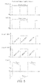
- the graphs on FIG.5 show different signals and illustrate different states of the transistors during one period of operation.
- the output signal VLX_1 ( FIG.5 ) is the sum of the output signals of the transistor PMOS SEGMENT_1 and NMOS_SEGMENT_1 when they are in the "ON" states.
- the range values of said output signal VLX_1 depends on the voltage value +VBAT.
- the frequency and the duty cycle of the signals CMD_P and CMD_N allow controlling the duration of conduction of each transistor such that if the low state duration of the signal CMD_P and CMD_N is higher then the duration of conduction of the transistor PMOS SEGMENT_1 will be longer and the duration of conduction of the transistor NMOS SEGMENT_1 will be shorter, and vice versa
- This principle of operation of the transistors is known by one with ordinary skills in the art as the commutation mode.
- the output power supply signal VLX_1 can be controlled by the duty cycle and the frequency of the signals CMD_P and CMD_N.
- the power losses are the sum of switching (dynamic) and ohmic or Joule (static) losses.
- the former stem from the necessity of driving the transistor parasitic gate capacitances commonly referred to as C G(N) and C G(P) .
- the later stem from parasitic resistances including intrinsic NMOS and PMOS channel resistances commonly referred to as the R ON(N) and R ON(P) resistances, in addition to the resistance of all metallic connections as the inductor or PCB one.
- a Simplified scheme of a Switched Power Supply Circuit containing these parasitic elements is shown on FIG.6 .
- a first current path named I ON(P) for the PMOS transistors, occurs during the PMOS transistors conduction phase.
- I ON(N) for the NMOS transistors occurs during the NMOS transistors conduction phase.
- R ON(N) and R ON(P) are the ON-channel resistances of the PMOS and NMOS transistors, respectively.
- R H and R L are the Source and Drain metallic access resistances of the transistors; and resistances R PCB,IN and R PCB.OUT being the sum of all remaining input and output wiring resistances, which are encountered in the current path of I ON(N) and I ON(P) ( e.g . PCB routing resistance, package access resistances, input filter).
- a capacitance C LX of the output of the Switched Power Supply Circuit is further shown on FIG.6 , which is usually dominated by the sum of NMOS and PMOS drain overlap and junction capacitances.
- An inductance (not shown) may be coupled to the capacitor and resistor of the Load module 500.
- R N.P are the total resistances related to the ohmic losses during the NMOS and PMOS conduction phases
- R P.N_SWITCH are the resistance of switches inside the package (MOS R ON with metallic access resistance).
- R N.P_EXT are the sum of all external resistances.
- TON is the conduction time of the related switch (PMOS or NMOS).
- the PED module 300 be adapted to create replica of the ohmic losses and compare it with switching losses occurring during said operation.
- the internal structure of a NMOS power transistor is different than the internal structure of the PMOS power transistor. Indeed, different doping solutions, internal structure and types of charge carriers are used during the conception of a NMOS or PMOS transistor. Hence, ohmic and switching losses are different in a PMOS transistor than in a NMOS transistor. To measure and create replica losses, a specific circuit for the peak-efficiency detection of the NMOS transistor and the PMOS transistor may be realised. In the following description, only the case of a NMOS transistor is described. Further, as shown on FIG.1 and FIG.2 , the input signal of the PED module 300 is provided by the output VLX, CMD_P and CMD_N of the SPS module 200.
- the PED module 300 (as shown in FIG.8 ) may be adapted to receive, on its inputs 301 and 302, the supply voltages +VBAT and Gnd , respectively, from the power supply source 100.
- An input 305 may be adapted to receive the output signal CMD_P
- an input 306 may be adapted to receive the output signal CMD_N from the SPS module 200
- another input 303 may be adapted to receive the output signal VLX from the SPS module 200
- still another two inputs 304 and 307 may be adapted to receive respectively the signal EN_P and the signal EN_N from the Power Stage Size control module 400.
- the PED module 300 may be adapted to provide on an output 304 an output signal named PEAK_D which is representative of the efficiency of the SPS module 200.
- the internal structure Fig. 8 of the PED module 300 can be divided in two main modules, such as a signal formatting module 310 ( Fig. 10 ), and a replica of ohmic losses module 320. These modules can comprise several internal functions provided by integrated electronic circuits such as resistors, capacitances, OAs, and transistors that they are described in more details below.
- the signal formatting module 310 comprises three modules, namely a first module named masking circuit module 316, a second module named Averaging module 312, and a third module named invert module 314.
- the masking circuit module 316 has an input 3161 coupled to the input 303 of the PED module 300, and said input is adapted to receive the signal V_LX from the SPS module 200.
- the masking circuit module 316 is adapted to provide a filtered signal named MASK on an output 3162.
- the average module 312 is adapted to receive on an input 3121 the signal MASK from the masking circuit module 316 and is adapted to provide an output signal named AVR on an output 3122 where, said output signal AVR is the average value of the signal MASK.
- the invert module 314 is adapted to receive on an input 3141 the signal AVR from the output of the average module 312 and to provide on an output 3142 an output signal named AVR_INV, that is to say the invert value of the input signal thereof.
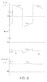
- the graph on FIG.9 shows the several output signals of the three modules of the signal formatting module 310.
- the masking circuit module 316 helps to remove the high voltage from the VLX signal so as to keep the NMOS signal only (signal across the NMOS ON resistance when this transistor is conducting).
- An example of electronic circuit performing this function is shown in FIG.10 .
- This electronic circuit comprises for instance an electronic inverter circuit named EIC_1 coupled to a first MOS transistor T1, and two other transistors named respectively T2 and T3.
- This electronic circuit senses the voltage across the NMOS switches when it is ON (conducting), provides the output signal MASK during the NMOS transistor conduction period T ON(N) . and sets the output 3162 to a high impedance in the remaining time.
- the second module named average module 312 provides on this output 3122 an average value of the input signal 3121 from the masking circuit module 316.
- the average function is made by a RC filter which provides an average voltage only during the transistor conduction (when transistor is 'ON'), and holds the average voltage on the filter capacitor afterwards.
- an invert value of the signal may be provided by the invert module 314.
- the invert module 314 may be adapted to invert the input signal AVR and to provide an output signal with an invert value of the AVR signal.
- This function can be obtained by an OPA (OPerational Amplifier) EIC_2 with an amplification gain of -1 ( FIG.10 ).
- one function of the PED module 300 is to create a replica of the ohmic and sand compare it to the switching losses during the conduction phase of the NMOS transistor of the SPS module 200.
- the NMOS replica ohmic losses module 322 may comprise an electronic circuit adapted to create a replica of all ohmic losses in the NMOS transistor, namely parasitic resistance losses and connection resistances losses, for instance.
- the NMOS replica ohmic losses module 322 is adapted to provide a replica output current of the NMOS transistor of the SPS circuit current during the conduction phase thereof.
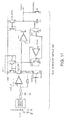
- a sense-FET transistor could be used for creating a replica current ( FIG.11 ).
- the sense-FET transistor named Sense_F may be designed with a scaled coefficient named ⁇ -scaled which allows to obtain scaled resistance (weighted by the ⁇ -scaled coefficient) to the ohmic resistance of the NMOS transistor used in the SPS Circuit 210 for instance.
- This sense-FET provides a replica current with a smaller area and a smaller consumption of current.
- an electronic circuit may allow to create a scaled auxiliary resistor named for instance Rx ( FIG.11 ).
- the two electronic circuits presented above allow to obtain the replica of the current though the Sense-FET independently of the duty cycle D of the output signal VLX .
- a copy resistor RN/ ⁇ arranged to provide the power dissipated in the power MOS transistor.
- the NMOS replica switching losses module 324 is adapted to receive on an input 3241 the signal OHMIC from the NMOS replica ohmic losses module 322 and is adapted to provide on an output 3242 an output signal named PEAK_D replica of the total losses (ohmic losses and switching losses) of the SPS module 200.
- the value of the auxiliary capacitor C' G(N) is determined during the conception of the NMOS replica switching losses module 324 and is in accordance with the intrinsic characteristics of the capacitor of the SPS circuit. An example of implementation is presented on FIG 11 .
- a ohmic replica losses module 310 is used. This ohmic replica losses module 310 is designed to create total ohmic replica losses for all SPS circuits configurations.
- a control signal from the Power size stage control module 400 in other embodiment of the invention could be used to select a part of all ohmic replica losses of the ohmic replica losses module 310 in accordance with the number of activated SPS circuits.
- the maximum peak efficiency appears when the ohmic losses are identical to the switches losses.
- the detection of operation at the peak efficiency relies on a circuit that allows to transfer the amount of power dissipated on the parasitic resistances to an auxiliary capacitor C' G(N) .
- auxiliary capacitors store identical amount of power as the power being dissipated on the resistance R N during one conduction cycle.
- the graph on FIG. 12 shows simulation results of a Peak Efficiency Detection device 1.
- simulations were performed with real NMOS power transistor mathematical models, with a linear sweep of the output current (load current) from 0 to 300mA.
- the integration time is T ON .
- the maximum peak efficiency was obtained when the voltage of the capacitors C' GS is equal to +VBAT.
- FIG.12 a zoom allows to highlight the different phases which enable to obtain the maximum peak efficiency.
- Three phases of operation are identified, namely:
- the phase No.1 allows to charge C' GS by a current I B during the time of the conduction of the Power NMOS transistor in SPS circuit.
- the charging of this capacitance is performed by a constant current and the duration of this charging is equal to the conduction time of related transistor.
- the phase No.2 allows to evaluate the voltage across the capacitor C' GS in the Power stage size control module 400 by comparator COMP_3. Further, as explained above, when the value of this signal is below the value +VBAT that signifies that the switching losses are dominating the ohmic losses and when the voltage value is above or in our case equal to +VBAT that signifies the ohmic losses are dominant compared to the switching losses.
- the regulations of these parameters are made by activating or disabling segments of the SPS circuit. We notice that V CAP reaches + VBAT at the point of maximum efficiency.
- the phase No.3 allows discharging the power stored in the capacitor C' GS quickly before another phase of efficiency regulation.
- This discharge of the capacitor C' GS could be performed by a transistor coupled in parallel to the said capacitor, and the discharge time is controlled by the internal resistor of the transistor.
- the power stage modulation strategy could be exploited in the following way:
- the Power stage size control module 400 comprises a comparator electronic circuit named COMP_3 and a shift register. This shift register is adapted to receive on an input the signal PEAK_D from the PED module 300 and to receive on a second input a clock signal CLK. It allows to activate or disable the SPS circuits 210, 220,..., 2N0 incrementally.
- the SPS module is configured to dynamically activate or deactivate at least one of the SPS circuits 210 operating to generate the output supply signal V_OUT on the internal central node N_2, when the signal PEAK_D representative of the efficiency of the SPS module is lower than threshold value (close to VBAT) meaning that the switching losses of the SPS module 200 are preponderant over the ohmic losses, or when said signal PEAK_D representative of the efficiency of the SPS module is higher than a second threshold value meaning that the ohmic losses of the SPS module 200 are preponderant over the switching losses, respectively.
- threshold value close to VBAT
- the regulation of the size of the SPS module 200 without implementing the proposed embodiments causes big jumps of the efficiency of the SPS module 200, represented by the continuous line, during the regulation phase of the SPS module. These jumps correspond to the activation of a second SPS circuit which changes the power efficiency from 25% to 100%.
- Another typical case without implementing the proposed embodiments is that the power-efficiency follows only 100% power-stage size.
- the regulation of the size of the SPS module 200 with the defined power regulation strategy and defined internal structure as explained above allows to avoid big jumps of the efficiency signal PEAK_D during the regulation phase of the SPS module 200 with the power stage size control module 400 as explained above.
- the curve in continuous line in FIG.14 exhibits faster, but smaller changes of the power efficiency obtained when the proposed regulation scheme is implemented.
- the proposed strategy optimise the power efficiency with respect to all main parameters having direct impact to the power efficiency value, as the input and output voltage V BAT /V OUT , output current I OUT , switching frequency F CLK , Temperature, and process variations.
Landscapes
- Engineering & Computer Science (AREA)
- Power Engineering (AREA)
- Dc-Dc Converters (AREA)
Abstract
Description
- The present invention generally relates to Switched Mode Power Supplies (SMPS), and more particularly to techniques of detecting a peak efficiency of a switched power stage.
- The approaches described in this section could be pursued, but are not necessarily approaches that have been previously conceived or pursued. Therefore, unless otherwise indicated herein, the approaches described in this section are not prior art to the claims in this application and are not admitted to be prior art by inclusion in this section.
- Switched Mode Power Supplies (SMPS) DC/DC converter are used in an increasing number of electronic applications, such as cellular phones, laptop computers, etc., due to their better efficiency than linear power supplies. Indeed, SMPS have lower power losses than linear power supplies. Another advantage of SMPS is their capability to provide a stabilized supply current or supply voltage to a load.
- Controlling the stability of the power supply signal is a very important challenge for SMPS manufacturers. Indeed, new electronic devices such as tablets or cellular phones, for instance, need a well stabilized continuous voltage supply despite variations of temperature and variations of power consumption during their use for a phone call or during a video recording, for instance. To meet these needs, it is necessary to control in continuous the voltage supplied to the electronic device and to adjust the operation of the SMPS.
- A solution allowing to control the supply voltage delivered to the load by an output stage of the SMPS can consist in monitoring in continuous the output voltage by an controller generation to the duty-cycle signal delivered to the power-stage made of power switches such as power MOS (Metal Oxyde Semiconductor) transistors.
- A main disadvantage of this solution, however, is that the output supply voltage cannot be efficiently controlled to accurately account for the intrinsic losses of the MOS transistors. Theses losses comprise static and dynamic contributions, namely conduction losses and switching losses, respectively. Indeed, with a view to increase the life-time of the battery, for instance, it is necessary to determine all losses of the SMPS in with respect to the power needs of the load. As a result, the size of the output stage can be dynamically optimized in order to avoid extra power-losses inside the SMPS during the discharge of the battery, due to the switching losses occurring during normal operation of the device.
- The present invention provides an alternative solution for controlling efficiency of the switched power supply module with aim to target best possible power-efficiency for given operating point. The system is both reliable and efficient, and in addition cheap to manufacture.
- According to a first aspect of the invention, there is proposed a Peak Efficiency Detection (PED) system comprising:
- a Switched Power Supply (power-stage) SPS, module adapted to provide an output supply signal of the device, comprising at least:
- ▪ an internal central node; and,
- ▪ a plurality of SPS circuits adapted to generate in combination the output supply signal on the internal central node,
- ▪ a Dead-time module adapted to generate two control signals with small non-overlap time,
- a central node external to the SPS module and adapted to deliver the output supply signal to a load module,
- a PED module adapted to receive the output supply signal from the central node, the control signals from the SPS module (CMD_P, CMD_N), signals from a Power stage size control module and to provide a signal PEAK_D representative of an efficiency of the SPS module, comprising at least:
- ▪ a Signal Formatting module adapted to provide a formatted signal from the output supply signal,
- ▪ a Replica Losses module adapted to provide a signal representative of ohmic and switching losses of the SPS module based on the formatted signal,
- the Power stage size control module adapted to provide at least two digital control signals (EN_N, EN_P) for controlling the SPS module,
- In an exemplary embodiment of the invention, the SPS circuits comprise at least one power switch, and this Power Switch is made by a power Metal Oxyde Semiconductor, MOS, transistor.
- In an exemplary of embodiment of the invention, data transfers are performed by a communication in order to allow communication between the PED module, the power stage size control module, and the SPS module.
- Moreover, in other exemplary embodiment of the invention, in order to obtain accurate replica Ohmic losses, the ohmic losses module comprises at least a sense-FET transistor configured to create a image of the current delivered to the output by the SPS circuits. This replica is done with a scale ratio in order to deliver a current helping to create a image of the ohmic losses of the SPS circuits.
- Further, in order to obtain accurate replica Switching losses, the Switching losses module comprises at least an auxiliary capacitor made by a MOS transistor (MOS capacitor) configured to be charged by the current representative of the ohmic losses of the SPS circuits and to derive the from of a voltage representative of the power-losses of the activated SPS circuits.
- In a second aspect of the invention, it is proposed a method of a Peak Efficiency Detection system, PED, for a Switched Mode Power Supply, SMPS, comprising:
- a Switched Power Supply, SPS, module providing an output supply signal of the device with
- ▪ at least some of a plurality of SPS Circuit generating in combination said output supply signal on an internal central node to the SPS module,
- ▪ a Dead time module providing two control signals (CMD_P and CMD_N),
- a central node external to the SPS module delivering the output signal to the load module,
- a PED module receiving the output supply signal from the central node, the control signals (CMD_P, CMD_N) from the SPS module, the signals (EN_N, EN_P) from a power stage size control module, and providing a signal PEAK_D representative of an efficiency of the SPS module, with:
- ▪ a Signal Formatting module providing a formatted signal from the output supply signal,
- ▪ a Replica Losses module providing a signal representative of ohmic and switching losses of the SPS module based on the formatted signal,
- a Power stage size control module providing at least two control signals (EN_P, EN_N) for controlling the SPS module, wherein the method further comprises:
- activating or deactivating at least one of the SPS circuits operating to generate the output supply signal on the internal central node, when the signal generated by the PED module and representative of the efficiency of the SPS module is lower than a threshold value meaning that the dynamic losses of the SPS module are preponderant over the ohmic losses, or when said signal representative of the efficiency of the SPS module is higher than the threshold value meaning that the ohmic losses of the SPS module are preponderant over the dynamic losses, respectively.
- In other exemplary embodiment of the invention the duration of conduction of the Switched Power Circuits is controlled by the control signals duty-cycle.
- In other exemplary embodiment of the invention each transistor of each SPS circuit is activated by a control signals.
- Embodiments of the present invention are illustrated by way of example, and not by way of limitation, in the figures of the accompanying drawings, in which like reference numerals refer to similar elements and in which:
-
FIG.1 is a simplified block diagram of a Switched-Mode Power Supply device containing the peak-efficiency module PED, according to an embodiment of the proposed solution, -
FIG.2 is a simplified block diagram of an embodiment of the SPS module (power-stage) with variable size of the device ofFIG.1 , -
FIG.3 is a simplified block diagram of one of a plurality of a SPS segments comprised in the SPS module ofFIG.2 , -
FIG.4 is a simplified block diagram of another embodiment of the SPS circuits, -
FIG.5 shows a sequence, as a function of time, of signals and voltages of the device according to embodiments, -
FIG.6 is more detailed circuit diagram showing the internal structure of a SPS circuit including the main losses elements, -
FIG.7 is a more simplified circuit diagram showing the internal structure of a SPS circuit including main losses elements, -
FIG.8 is a simplified block diagram of a PED module according to another embodiment, -
FIG.9 shows a sequence, as a function of time, of signals and voltages the device according to embodiments, -
FIG.10 is an example of internal electronic circuitry of a first main module of the PED module, -
FIG.11 is an example of internal electronic circuitry of a second main module of the Peak Efficiency module embodying another proposed solution, -
FIG.12 is a graph representing the simulation of the Peak Detention embodying the proposed solution, -
FIG.13 is a block diagram of the internal electronic circuitry of the Power stage size control module (Peak-Efficiency Tracking) according to another embodiment bodying another the proposed solution, -
FIG.14 are graphs comparing the power efficiency of a Switched Power Supply module not embodying, or embodying, respectively, the proposed power regulation strategy. - Embodiments as described herein are directed to a device and a method for adjusting automatically the number of Switched Power Supply (SPS) circuits, also referred to as power stages segments, to obtain optimal peak efficiency of a SPS module.
- Referring to
FIG.1 , there is shown therein a simplified bloc diagram of a Peak Efficiency Detection (PED)device 1 containing also the power-stage module, to which embodiments of the invention can be applied. - The proposed
PED device 1 may be run upon a start-up of electronic devices such as a tablet for instance, supplied by a Switched Mode Power Supply (SMPS) embodying saiddevice 1. Indeed, the SMPS device has applications for controlling a current or a voltage supply delivered to a load when, for instance, the temperature of electronic components vary during the device run or when the activity of the electronic device increases, for instance, during a power consuming phase of operation such as video recording. - In one embodiment of the invention, the
PED device 1 comprises three main blocks such as a first main block named SPS module, a power-stage 200 and adapted to provide a output voltage VLX to a Filter-module 600, a second main block namedPED module 300 and adapted to provide a signal named PEAK_D representing the efficiency of theSPS module 200, and a third main block named Power stagesize control module 400 and adapted to provide a first control signal named EN_P and a second control signal named EN_N for controlling the amount of activatedSPS module 200 and thePED module 300 in function of a determined strategy which will be described in more details below. - Further, the
PED device 1 comprises two input terminals K1 and K2 coupled to a powersupply voltage source 100, and two output terminals K3 and K4 to which aFilter module 600 is coupled. - Furthermore, the
PED device 1 comprises an internal central node N_1 adapted to dispense the power supply signal VLX from theSPD module 200 to thePED module 300 and to theLoad module 500 through theFilter module 600. - The
source 100 may be a battery or another type of power supply voltage generator able to provide one DC voltage such as voltage +VBAT referenced to Gnd. Thesource 100 is coupled to the input terminals K1 and K2, respectively, of thedevice 1. In the shown example, the powersupply voltage generator 100 comprises an internal parasitic resistor R_BAT representative of the total internal resistance of thegenerator 100. TheLoad module 500 could be an electronic circuit of a cellular phone or a laptop computer, for instance. These examples are not restrictive of the many applications of the proposed device. - The
Filter module 600, placed between the output terminal K3 and theLoad module 500 comprises an inductor (L) coupled with a capacitor (C) allows to obtain a particular cut-off frequency determinate by the inductor and capacitor values. TheFilter module 600 is adapted to receive the output signal VLX from the central node N_1 through the output terminal K3, and is adapted to provide a smoothed signal named V_OUT to an input of theLoad module 500. TheFilter module 600 can use several additional components (capacitors, resistors, and inductances), and these components could be integrated during the conception on a silicon chip of thePED device 1. - The
SPS module 200 as shown onFIG.2 comprises a plurality ofSPS circuits Dead time module 800, twopower supply inputs inputs size control module 400, aninput 205 adapted to receive a signal named Duty_Cycle allows to control the duration of conduction of the switched power supply circuits., anoutput 209 adapted to provide the supply signal named VLX to the central node N_1 of thePED device 1, and twooutputs SPS module 200 comprises an internal central node N_2 which is identical as N_1 node. - The
Dead time module 800 is adapted to receive on aninput 802 the Duty_cycle signal form an external controller, and is adapted to provide on a first output 804 a signal named CMD_P and on a second output 806 a signal named CMD_N. These signals are slightly non-overlapping. The frequency and duration of a high state of the Duty_cycle signal are adjustable by an external controller. - The
SPS circuit 210, is adapted to receive oninputs 216 and 217 two input signals from theDead time module 800 with the first input signal named CMD_P enables to control the duration of conduction of a transistor PMOS of the switchedpower supply circuit 210 and the second input signal named CMD_N that enables to control the duration of conduction of a transistor NMOS of the said circuit.. The switchedpower supply circuit 210 comprises anoutput 215 adapted to provide a supply signal named VLX_1 to the internal central node N_2 of the switchedpower supply module 200. - The Switched
Power Supply Circuit 220, for instance, comprises twoinputs Dead time module 800 that enable to control the duration of conduction of PMOS and NMOS transistors of the said circuit. Furthermore, the switchedpower supply circuit 220 comprises two anotherinputs EN_N 220 from the from the Power stagesize control module 400 through theinputs SPS module 200. These signals (EN_P220 and EN_N220) allow activating or disabling each transistor of each SPS circuit in function of a defined power regulation strategy that will be described in more details below. TheSPS circuit 220 comprises anoutput 225 adapted to provide a signal VLX_2 of theSPS module 200 as its contribution to the generated output supply voltage VLX. The signal VLX is representative in the following description to the power delivered by all activated SPS circuit (210, 220,..., 2N0) of theSPS module 200. - For the sake of simplicity of the present description, only the
SPS circuit 220 has been described but it will be appreciated that, referring to theFIG.2 all SPS circuits (without the switched power supply circuit 210) may have same internal characteristics and same internal design (circuits, components). Furthermore, the number of SPS circuits and their characteristics are defined during the design of theSPS module 200 depending on the specific application. To that end, they may be integrated in a same chip for reaching a minimum mismatch of characteristics. Further, all outputs of all SPS circuits are coupled to the internal central node N_2 of the SwitchedPower Supply module 200. - Referring to
FIG.1 , the Power stagesize control module 400 comprises oneinput 404 adapted to receive the signal PEAK_D from an output of thePED module 300, and comprises twooutputs - As presented above, one of the goals of the
PED module 300 is to detect the peak efficiency of theSPS module 200. To that end, all losses in theSPS circuit 200 are determined during the operation of theSPS module 200 in order, for instance, to avoid the useless power losses. The efficiency of the device is mainly determined by the configuration of theSPS module 200, particularly size of the associated power MOS transistors. Mainly two set points can control the efficiency of theSPS module 200. - The first point of control is the size of the structure, which may be optimised during the conception of power MOS transistors used in the
SPS module 200 and their associated circuitry. Further, the number of activated SPS circuits may be dynamically adapted as a function of the power needs of theload 500. - The second point which allows obtaining high efficiency of the
SPS module 200 is the Power stagesize Control module 400. Indeed, this module enables to activate or disable each power MOS transistor of the SPS circuits depending on the power requirement of theload 500 and other parameter of the circuit. The said Power stagesize control module 400 is adapted to provide several control signals to theSPS module 200 in order to control the number of activated Switched Power Stage Circuits, and the duration of the conduction of said SPS Circuits. The Power stagesize control module 400 presented above is adapted to monitor several parameters such as number of activated subscircuits and duration of conduction of PMOS and NMOS transistors of theSPS module 200 for controlling the output supply signal VLX. - The power supply signal VLX (as shown on
FIG.2 ) provided by theSPS module 200 results from the addition of the contributions provided by the activated SPS circuits summed at the internal central node N_2 according to the Kirchoff laws. The activation of each PMOS and NMOS transistors of the SPS circuits in accordance with a power regulation strategy is performed by signals EN_N and EN_P. A direct connection by thecommunication bus 12 may be used to provide the EN_N and EN_P signals. In these examples, the EN_N and EN_P signals can comprise an address signal and a command signal allowing to activate or disable each of the SPS subcircuits in function of the defined strategy. - Two another parameters may allow controlling the power supply signal VLX such as the frequency and the duty cycle of the signals CMD_P and CMD_N. For explaining the influence of these parameters on the power supply signal VLX the internal structure of a Switched Power Supply Circuit will be first described.
-
FIG.3 and FIG.4 show two examples of internal structure of a SPS circuit andFIG.5 shows various associated signals. It will be appreciated that only theSPS circuit 220 will be described in details, said description being valid for the other SPS subcircuits as well. Furthermore, it will be appreciated that, onFIG.5 , the duty cycle of signals CMD_P and CMD_N is equal to 0.5. - The
SPS circuit 210 shown inFIG.3 comprises two power MOS transistors with a first PMOS transistor PMOS_SEGMENT_1, a second NMOS transistor NMOS_SEGMENT_1. A gate of the transistor PMOS_SEGMENT_1 is coupled to theinput 214 of the switchedpower supply circuit 210 and is adapted to be controlled by the signal CMD_P. A gate of the transistor NMOS_SEGMENT_1 is coupled to theinput 213 of the said circuit and is adapted to be controlled by the signal CMD_N. Further, a source of the transistor PMOS_SEGMENT_1 is coupled to a VBAT, and source of the transistor NMOS_SEGMENT_1 to GND. A node named N_210 on theFIG.3 placed between the drains of the two transistors is adapted to dispense the signal VLX_1 through theoutput 215 of the switchedpower supply circuit 1. As the transistors in this segment are hard connected to the CMD_P and CMD_N signals, this first segment is always active (means that it cannot be deactivated) - The switched
power supply circuit 220 shown onFIG.4 comprises two MOS transistors with a first transistor PMOS_SEGMENT_2, and a second transistor NMOS_SEGMENT_2, and comprises two logical structures named logical_221 and logical 222. The logical structure _221 is adapted to receive on a first input 221_1 the signal CMD_P from theDead time module 800 and on a second input named 221_2 the signal EN_P2 from the Power stagesize control module 400. Thelogical structure 221 is adapted to provide on an output 221_3 a signal representative of an OR-type boolean calculation between the said two input signals. The output 221_3 of the structure logical 221 is coupled to a gate of the PMOS_SEGMENT_2 transistor. - The structure logical_222 is adapted to receive on a first input 222_1 the signal CMD_N from the
dead time module 800 and on a second input named 222_2 the signal EN_N2 from the Power stagesize control module 400. The logical structure _222 is adapted to provide on an output 222_3 a signal representative of an AND-type boolean calculation between the said two input signals. The output 222_3 of the structure logical 222 is coupled to a gate of the NMOS_SEGMENT_2 transistor. - Further, a node named N_220 on the
FIG.5 placed between the drains of the two transistors is adapted to provide the signal VLX_2 through theoutput 225 of the switchedpower supply circuit 2. - In one embodiment, the signals CMD_P and CMD_N of the
inputs 12 and 14 have the same shape (as shown inFIG.5 ). In other embodiment, a delay may be created between the two signals CMD_P and CMD_N, this delay allowing to avoid any risk of crossconduction due to the simultaneous conduction of the two transistors. - The graphs on
FIG.5 show different signals and illustrate different states of the transistors during one period of operation. The output signal VLX_1 (FIG.5 ) is the sum of the output signals of the transistor PMOS SEGMENT_1 and NMOS_SEGMENT_1 when they are in the "ON" states. The range values of said output signal VLX_1 depends on the voltage value +VBAT. - In other embodiment, the frequency and the duty cycle of the signals CMD_P and CMD_N allow controlling the duration of conduction of each transistor such that if the low state duration of the signal CMD_P and CMD_N is higher then the duration of conduction of the transistor PMOS SEGMENT_1 will be longer and the duration of conduction of the transistor NMOS SEGMENT_1 will be shorter, and vice versa This principle of operation of the transistors is known by one with ordinary skills in the art as the commutation mode. Thereby, the output power supply signal VLX_1 can be controlled by the duty cycle and the frequency of the signals CMD_P and CMD_N.
- Like in all DC/DC converters the power losses are the sum of switching (dynamic) and ohmic or Joule (static) losses. The former stem from the necessity of driving the transistor parasitic gate capacitances commonly referred to as C G(N) and C G(P). The later stem from parasitic resistances including intrinsic NMOS and PMOS channel resistances commonly referred to as the R ON(N) and R ON(P) resistances, in addition to the resistance of all metallic connections as the inductor or PCB one. A Simplified scheme of a Switched Power Supply Circuit containing these parasitic elements is shown on
FIG.6 . - In this Figure, two current paths are represented. A first current path, named ION(P) for the PMOS transistors, occurs during the PMOS transistors conduction phase. A second current path named ION(N) for the NMOS transistors occurs during the NMOS transistors conduction phase. RON(N) and RON(P) are the ON-channel resistances of the PMOS and NMOS transistors, respectively. RH and RL are the Source and Drain metallic access resistances of the transistors; and resistances RPCB,IN and RPCB.OUT being the sum of all remaining input and output wiring resistances, which are encountered in the current path of ION(N) and ION(P) (e.g. PCB routing resistance, package access resistances, input filter). A capacitance CLX of the output of the Switched Power Supply Circuit is further shown on
FIG.6 , which is usually dominated by the sum of NMOS and PMOS drain overlap and junction capacitances. An inductance (not shown) may be coupled to the capacitor and resistor of theLoad module 500. - For a better understanding, the equivalent circuit on the
FIG.6 can be simplified into the circuit shown inFIG.7 . In this schematic, RN.P are the total resistances related to the ohmic losses during the NMOS and PMOS conduction phases, and RP.N_SWITCH are the resistance of switches inside the package (MOS RON with metallic access resistance). Further, RN.P_EXT are the sum of all external resistances. The losses in aSPS module 200 composed by power MOS transistors are characterized by:

where: - R is the average resistance of the system,
- C is the sum of all parasitic capacitances (charge/discharged) with fCLKrate,
- fCLK is the clock frequency of the Duty_cycle signal,
- lout is the DC output current,
- D is the high state of the Duty_cycle signal, and
- (1-D) is the low state of the Duty_cycle signal.
- The proposed device and method allow determining the maximum peak efficiency of the
SPS module 200, by derivating the output current named lout inequation 2, so that:
where: - η is the efficiency of the Supply Power Stage defined as η = Pout/Pin,
- IOUT is the output current.
- The output current corresponding to the peak efficiency operations of a given power switch (i.e. PMOS or NMOS)results from previous as:

- Where TON is the conduction time of the related switch (PMOS or NMOS). The formula presented above signifies that the peak efficiency occurs when switching and ohmic losses are equal, namely when:

- The real joule power dissipated during conduction cycles of NMOS switch resistance RN_SWITCH can be then obtained as:

- Applying the recopied current αIout to resistance RN/α (integrated inside the PED) allow to reconstitute voltage drop related to total joule losses during the NMOS conduction cycle. This voltage is then:

- And the joule losses due to the NMOS condition phase are therefore:

- Considering the short mathematical demonstration presented above, it will be appreciated that the ohmic losses and switching losses have to be identified and estimated during operation of the SPS circuit. In one embodiment of the invention, it is proposed that the
PED module 300 be adapted to create replica of the ohmic losses and compare it with switching losses occurring during said operation. - The internal structure of a NMOS power transistor is different than the internal structure of the PMOS power transistor. Indeed, different doping solutions, internal structure and types of charge carriers are used during the conception of a NMOS or PMOS transistor. Hence, ohmic and switching losses are different in a PMOS transistor than in a NMOS transistor. To measure and create replica losses, a specific circuit for the peak-efficiency detection of the NMOS transistor and the PMOS transistor may be realised. In the following description, only the case of a NMOS transistor is described. Further, as shown on
FIG.1 andFIG.2 , the input signal of thePED module 300 is provided by the output VLX, CMD_P and CMD_N of theSPS module 200. - The PED module 300 (as shown in
FIG.8 ) may be adapted to receive, on itsinputs power supply source 100. Aninput 305 may be adapted to receive the output signal CMD_P, aninput 306 may be adapted to receive the output signal CMD_N from theSPS module 200, while anotherinput 303 may be adapted to receive the output signal VLX from theSPS module 200, and still another twoinputs Size control module 400. Further, thePED module 300 may be adapted to provide on anoutput 304 an output signal named PEAK_D which is representative of the efficiency of theSPS module 200. - For a better understanding of the invention, in the following description only the case with a
peak efficiency module 300 for a NMOS transistor is described. - The internal structure
Fig. 8 of thePED module 300 can be divided in two main modules, such as a signal formatting module 310 (Fig. 10 ), and a replica ofohmic losses module 320. These modules can comprise several internal functions provided by integrated electronic circuits such as resistors, capacitances, OAs, and transistors that they are described in more details below. - In order to discriminate in the VLX signal the duration of the conduction of the PMOS transistors and the duration of conduction of the NMOS transistors, the
signal formatting module 310 comprises three modules, namely a first module named maskingcircuit module 316, a second module namedAveraging module 312, and a third module namedinvert module 314. - The
masking circuit module 316 has aninput 3161 coupled to theinput 303 of thePED module 300, and said input is adapted to receive the signal V_LX from theSPS module 200. Themasking circuit module 316 is adapted to provide a filtered signal named MASK on anoutput 3162. - The
average module 312 is adapted to receive on aninput 3121 the signal MASK from the maskingcircuit module 316 and is adapted to provide an output signal named AVR on anoutput 3122 where, said output signal AVR is the average value of the signal MASK. Theinvert module 314 is adapted to receive on aninput 3141 the signal AVR from the output of theaverage module 312 and to provide on anoutput 3142 an output signal named AVR_INV, that is to say the invert value of the input signal thereof. - The graph on
FIG.9 shows the several output signals of the three modules of thesignal formatting module 310. Themasking circuit module 316 helps to remove the high voltage from the VLX signal so as to keep the NMOS signal only (signal across the NMOS ON resistance when this transistor is conducting). An example of electronic circuit performing this function is shown inFIG.10 . This electronic circuit comprises for instance an electronic inverter circuit named EIC_1 coupled to a first MOS transistor T1, and two other transistors named respectively T2 and T3. This electronic circuit senses the voltage across the NMOS switches when it is ON (conducting), provides the output signal MASK during the NMOS transistor conduction period TON(N). and sets theoutput 3162 to a high impedance in the remaining time. - Estimating the losses in the NMOS transistor, is based on the averaging during one conduction cycle. Therefore, the second module named
average module 312 provides on thisoutput 3122 an average value of theinput signal 3121 from the maskingcircuit module 316. OnFIG.11 , an example of electronic circuit performing this function is shown. The average function is made by a RC filter which provides an average voltage only during the transistor conduction (when transistor is 'ON'), and holds the average voltage on the filter capacitor afterwards. - For a simplest circuitry of the
PED module 300, an invert value of the signal may be provided by theinvert module 314. To that end, theinvert module 314 may be adapted to invert the input signal AVR and to provide an output signal with an invert value of the AVR signal. This function can be obtained by an OPA (OPerational Amplifier) EIC_2 with an amplification gain of -1 (FIG.10 ). - All electronics circuits and circuitries presented above for the
modules - As explained above, one function of the
PED module 300 is to create a replica of the ohmic and sand compare it to the switching losses during the conduction phase of the NMOS transistor of theSPS module 200. - In one embodiment, the NMOS replica ohmic losses module 322 (
FIG.9 ) may comprise an electronic circuit adapted to create a replica of all ohmic losses in the NMOS transistor, namely parasitic resistance losses and connection resistances losses, for instance. The NMOS replicaohmic losses module 322 is adapted to provide a replica output current of the NMOS transistor of the SPS circuit current during the conduction phase thereof. As will be appreciated by the one skilled in the art, a sense-FET transistor could be used for creating a replica current (FIG.11 ). - To obtain a replica current, the sense-FET transistor named Sense_F may be designed with a scaled coefficient named α-scaled which allows to obtain scaled resistance (weighted by the α-scaled coefficient) to the ohmic resistance of the NMOS transistor used in the
SPS Circuit 210 for instance. This sense-FET provides a replica current with a smaller area and a smaller consumption of current. - As explained above several ohmic losses appear during the conduction of the NMOS transistor. In other embodiment an electronic circuit may allow to create a scaled auxiliary resistor named for instance Rx (
FIG.11 ). - The two electronic circuits presented above allow to obtain the replica of the current though the Sense-FET independently of the duty cycle D of the output signal VLX.
- To fully estimate and replicate all ohmic losses in a SPS module, it is possible to create a copy resistor RN/α arranged to provide the power dissipated in the power MOS transistor. In one embodiment, there is created a "sense" resistor RN/α with a gain alpha α (
FIG.11 ). An important fact is that the current passing through the scaled sense-FET is the absolute-value replica of the output current, i.e. has no duty-cycle dependency, and the real power dissipated during the conduction cycles of NMOS transistor is equal to a resistance RNMOS
- Applying the recopied current αIout to resistance RN/α allow to reconstitute voltage drop related to total joule losses during the NMOS conduction cycle. This voltage is then:

- The joule losses due to the NMOS condition phase are therefore:

- The method allowing to detect the peak efficiency operation presented here relies on a circuit, that allows to transfer the amount of energy dissipated on the parasitic resistance RN to an auxiliary capacitor


- The methodology introduced here is demonstrated on the NMOS part of the power switch. However, as already mentioned, two independent circuit allowing efficiency optimisation of NMOS and PMOS power switches are to be implemented.
- The principle of the method can appear from the definition of the work required to establish a defined voltage across the capacitor plates. This work can be developed as:

- From physical definition, electrical charge Q is defined as the current by time product. On this account, the last term in Eq.(9) can be written into following (unusual) form:

where IB is constant bias current which is to be applied to the auxiliary capacitor
- In the process of capacitor charging, half to the energy is dissipated on the resistive switch and half is stored in the capacitor. On this account, term ½ in Eq.(9) disappear. Now, we can be combined with Eq. (8) resulting in the energy balance:

- Eq. 11 can be simplified by decreasing the time of integration from TCLK to (1-D)TCLK. Then TON(N)=TCLK(1-D) and Eq. 11 results in:

- By rearranging this Eq.(12), we can obtain the bias current value:
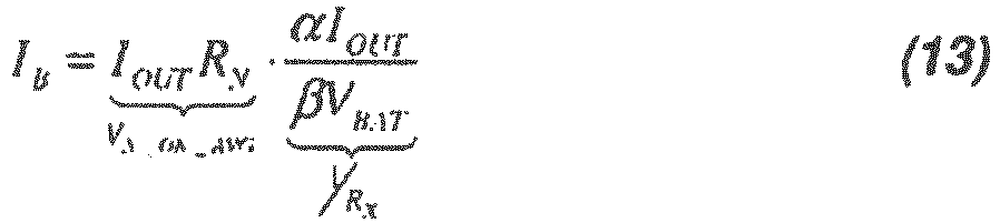
- If such current is applied to the capacitor

- In fact, Eq. (13) allows to realise linear circuit allowing to measure the average energy dissipated on the RN resistance during one clock period, and to store identical amount of energy in the auxiliary capacitor

- For that, the NMOS replica
switching losses module 324 is adapted to receive on aninput 3241 the signal OHMIC from the NMOS replicaohmic losses module 322 and is adapted to provide on anoutput 3242 an output signal named PEAK_D replica of the total losses (ohmic losses and switching losses) of theSPS module 200. This module may use an auxiliary capacitor C'G(N) where:
- The value of the auxiliary capacitor C'G(N) is determined during the conception of the NMOS replica
switching losses module 324 and is in accordance with the intrinsic characteristics of the capacitor of the SPS circuit. An example of implementation is presented onFIG 11 . - In other embodiment, a ohmic
replica losses module 310 is used. This ohmicreplica losses module 310 is designed to create total ohmic replica losses for all SPS circuits configurations. A control signal from the Power sizestage control module 400 in other embodiment of the invention could be used to select a part of all ohmic replica losses of the ohmicreplica losses module 310 in accordance with the number of activated SPS circuits. - As explained above, the maximum peak efficiency appears when the ohmic losses are identical to the switches losses. The detection of operation at the peak efficiency relies on a circuit that allows to transfer the amount of power dissipated on the parasitic resistances to an auxiliary capacitor C'G(N). When both power are balanced (power required to charge capacitor C G(N) and Joule power dissipated on RN during one conduction cycle), then the capacitor

- The graph on
FIG. 12 shows simulation results of a PeakEfficiency Detection device 1. In order to describe operation of thedevice 1, simulations were performed with real NMOS power transistor mathematical models, with a linear sweep of the output current (load current) from 0 to 300mA. In these simulations, the integration time is TON. The maximum peak efficiency was obtained when the voltage of the capacitors C'GS is equal to +VBAT. - In
FIG.12 a zoom allows to highlight the different phases which enable to obtain the maximum peak efficiency. Three phases of operation are identified, namely: - Phase No.1:
- integration time, when current IB is applied to

- Phase No.2:
- evaluation phase, when the capacitor holds the integrated voltage value and value of the integrated voltage is evaluated, and
- Phase No.3:
- capacitor reset phase.
- The phase No.1 allows to charge C'GS by a current IB during the time of the conduction of the Power NMOS transistor in SPS circuit. The charging of this capacitance is performed by a constant current and the duration of this charging is equal to the conduction time of related transistor.
- The phase No.2 allows to evaluate the voltage across the capacitor C'GS in the Power stage
size control module 400 by comparator COMP_3. Further, as explained above, when the value of this signal is below the value +VBAT that signifies that the switching losses are dominating the ohmic losses and when the voltage value is above or in our case equal to +VBAT that signifies the ohmic losses are dominant compared to the switching losses. The regulations of these parameters are made by activating or disabling segments of the SPS circuit. We notice that VCAP reaches +VBAT at the point of maximum efficiency. - The phase No.3 allows discharging the power stored in the capacitor C'GS quickly before another phase of efficiency regulation. This discharge of the capacitor C'GS could be performed by a transistor coupled in parallel to the said capacitor, and the discharge time is controlled by the internal resistor of the transistor.
- In one embodiment of the invention, the power stage modulation strategy could be exploited in the following way:
- real time power stage size tuning.
- This allow regulate he size of the power stage with a defined power regulation strategy for obtaining an optimal peak efficiency of the SPS module.
- In there embodiment of the invention, a real time tuning of the size of the power supply stage is performed, as shown on
FIG. 13 an example of electronic circuit. The Power stagesize control module 400 comprises a comparator electronic circuit named COMP_3 and a shift register. This shift register is adapted to receive on an input the signal PEAK_D from thePED module 300 and to receive on a second input a clock signal CLK. It allows to activate or disable theSPS circuits - To summarized the SPS module is configured to dynamically activate or deactivate at least one of the
SPS circuits 210 operating to generate the output supply signal V_OUT on the internal central node N_2, when the signal PEAK_D representative of the efficiency of the SPS module is lower than threshold value (close to VBAT) meaning that the switching losses of theSPS module 200 are preponderant over the ohmic losses, or when said signal PEAK_D representative of the efficiency of the SPS module is higher than a second threshold value meaning that the ohmic losses of theSPS module 200 are preponderant over the switching losses, respectively. - This is explained with reference to
FIG.14 . There are shown therein three curves in dotted lines corresponding to the power efficiency of the SPS module having three size activated: 25%, 50% and 100%, respectively, of the SPS module. - As shown in
FIG.14 , the regulation of the size of theSPS module 200 without implementing the proposed embodiments causes big jumps of the efficiency of theSPS module 200, represented by the continuous line, during the regulation phase of the SPS module. These jumps correspond to the activation of a second SPS circuit which changes the power efficiency from 25% to 100%. Another typical case without implementing the proposed embodiments is that the power-efficiency follows only 100% power-stage size. - As shown in
FIG.14 , the regulation of the size of theSPS module 200 with the defined power regulation strategy and defined internal structure as explained above allows to avoid big jumps of the efficiency signal PEAK_D during the regulation phase of theSPS module 200 with the power stagesize control module 400 as explained above. Thus, the curve in continuous line inFIG.14 exhibits faster, but smaller changes of the power efficiency obtained when the proposed regulation scheme is implemented. Moreover, the proposed strategy optimise the power efficiency with respect to all main parameters having direct impact to the power efficiency value, as the input and output voltage VBAT/VOUT, output current IOUT, switching frequency FCLK, Temperature, and process variations. - While the invention has been illustrated and described in details in the drawings and foregoing description, such illustration and description have to be considered as illustrative or exemplary and not restrictive; the invention is not limited to the disclosed embodiments. Variations to the disclosed embodiments can be understood and effected by those skilled in the art in practicing the claimed invention, from a study of the drawings, the disclosure, and the appended claims. In the claims, the word "comprising" does not exclude other elements or steps, and the indefinite article "a" or "an" does not exclude a plurality. A single or a plurality of programmable circuit or other unit may fulfil the functions of several items recited in the claims. The mere fact that certain measures are recited in mutually different dependent claims does not indicate that a combination of these measures cannot be used to advantage.
Claims (9)
- A device (1) for Peak Efficiency Detection, PED, for a Switched Mode Power Supply, SMPS, comprising:- a Switched Power Supply, SPS, module (200) adapted to provide an output supply signal (VLX) of the device, comprising at least:▪ an internal central node (N_2); and,▪ a plurality of SPS circuits (210) adapted to generate in combination the output supply signal (VLX) on the internal central node (N_2),▪ a Dead time module (800) adapted to generate two control signals (CMD_P) and (CMD_N) with a small non-overlap time,- a central node (N_1) external to the SPS module and adapted to deliver the output supply signal to a load module (500),- a PED module (300) adapted to receive the output supply signal (VLX) from the central node (N_1), the control signals (CMD_P) and (CMD_N) from the SPS module (200), signals (EN_P, EN_N) from a Power stage size control module (400) and to provide a signal (PEAK_D) representative of an efficiency of the SPS module (200), comprising at least:▪ a Signal Formatting module (310) adapted to provide a formatted signal from the output supply signal,▪ a Replica Losses module (320) adapted to provide a signal representative of ohmic and switching losses of the SPS module (200) based on the formatted signal,- the Power stage size control module (400) adapted to provide at least two control signals (EN_P, EN_N) for controlling the SPS module (200),wherein, the SPS module is configured to activate or deactivate at least one of the SPS circuits (210) operating to generate the output supply signal (VLX) on the internal central node (N_2), when the signal (PEAK_D) generated by the PED module (300) and representative of the efficiency of the SPS module is lower than a threshold value meaning that the dynamic losses of the SPS module (200) are preponderant over the ohmic losses, or when said signal (PEAK_D) representative of the efficiency of the SPS module is higher than the threshold value meaning that the ohmic losses of the SPS module (200) are preponderant over the dynamic losses, respectively.
- The device of claim 1, wherein the SPS circuits (210) comprise at least one power switch.
- The device of claim 2, wherein the power switch comprises a power Metal Oxyde Semiconductor, MOS, transistor.
- The device of claims 1 to 3, further comprising serial communication means (12, 14) adapted to allow communication between the PED module (300), the power stage size control module (400), and the SPS module (200).
- The device of claims 1 to 4, wherein the ohmic losses module (310) comprises at least a copy transistor (Sense_F) configured to replicate a current through the SPS circuits with a scale ratio and to derive there from a current representative of the ohmic losses of the activated SPS circuits (210,220,...2N0).
- The device of claims 1 to 5, wherein the switching losses module (300) comprises at least an auxiliary capacitor (CLX) configured to be charged by the current representative of the ohmic losses of the SPS circuits and to derive there from a voltage signal representative of the switching losses of the activated SPS circuits (210,220,...2N0).
- A method of Peak Efficiency Detection, PED, for a Switched Mode Power Supply, SMPS, comprising:- a Switched Power Supply, SPS, module (200) providing an output supply signal (VLX) of the device with▪ at least some of a plurality of SPS Circuit (210) generating in combination said output supply signal (VLX) on an internal central node (N_2) internal to the SPS module,▪ a Dead time module (800) providing two control signals (CMD_P and CMD_N),- a central node (N_1) external to the SPS module delivering the output signal (VLX) to the load module (500),- a PED module (300) receiving the output supply signal from the central node (N_1), the control signals (CMD_P, CMD_N) from the SPS module (200), the signals (EN_N, EN_P) from a power stage size control module (400), and providing a signal (PEAK_D) representative of an efficiency of the SPS module (200), with:▪ a Signal Formatting module (310) providing a formatted signal from the output supply signal,▪ a Replica Losses module (320) providing a signal representative of ohmic and switching losses of the SPS module (200) based on the formatted signal,- a Power stage size control module (400) providing at least two control signals (EN_P, EN_N) for controlling the SPS module (200),wherein the method further comprises:- activating or deactivating at least one of the SPS circuits (210) operating to generate the output supply signal on the internal central node (N_2), when the signal (PEAK_D) generated by the PED module and representative of the efficiency of the SPS module is lower than a threshold value meaning that the dynamic losses of the SPS module (200) are preponderant over the ohmic losses, or when said signal (PEAK_D) representative of the efficiency of the SPS module is higher than the threshold value meaning that the ohmic losses of the SPS module (200) are preponderant over the dynamic losses, respectively.
- The method of Peak Efficiency Detection of claim 7, wherein the duration of conduction of the SPS circuits is controlled by (CMD_P, CMD_N) control signals.
- The method of Peak Efficiency Detection of claims 7 and 8, wherein each transistor of each SPS circuit is activated by (EN_P, EN_N) signals.
Priority Applications (2)
| Application Number | Priority Date | Filing Date | Title |
|---|---|---|---|
| EP20130306449 EP2863526A1 (en) | 2013-10-21 | 2013-10-21 | Switched mode power supply peak-efficiency detection |
| US14/518,039 US9537395B2 (en) | 2013-10-21 | 2014-10-20 | Switched mode power supply peak-efficiency detection |
Applications Claiming Priority (1)
| Application Number | Priority Date | Filing Date | Title |
|---|---|---|---|
| EP20130306449 EP2863526A1 (en) | 2013-10-21 | 2013-10-21 | Switched mode power supply peak-efficiency detection |
Publications (1)
| Publication Number | Publication Date |
|---|---|
| EP2863526A1 true EP2863526A1 (en) | 2015-04-22 |
Family
ID=49518892
Family Applications (1)
| Application Number | Title | Priority Date | Filing Date |
|---|---|---|---|
| EP20130306449 Ceased EP2863526A1 (en) | 2013-10-21 | 2013-10-21 | Switched mode power supply peak-efficiency detection |
Country Status (2)
| Country | Link |
|---|---|
| US (1) | US9537395B2 (en) |
| EP (1) | EP2863526A1 (en) |
Cited By (1)
| Publication number | Priority date | Publication date | Assignee | Title |
|---|---|---|---|---|
| CN114994441A (en) * | 2022-06-06 | 2022-09-02 | 重庆伏特猫科技有限公司 | Intelligent electric power efficiency monitoring device |
Families Citing this family (3)
| Publication number | Priority date | Publication date | Assignee | Title |
|---|---|---|---|---|
| US9444281B2 (en) * | 2014-01-03 | 2016-09-13 | Apple Inc. | Unified high power and low power battery charger |
| US10033272B2 (en) * | 2015-03-12 | 2018-07-24 | Qualcomm Incorporated | Switching loss correction circuitry and method |
| CN115848200B (en) * | 2023-02-06 | 2023-05-16 | 石家庄科林电气股份有限公司 | Group control charging system and control method thereof |
Citations (4)
| Publication number | Priority date | Publication date | Assignee | Title |
|---|---|---|---|---|
| US20080111529A1 (en) * | 2006-11-10 | 2008-05-15 | Dell Products L.P. | Methods, apparatus and media for control scheme for parallel high-side switching mosfets |
| WO2008135637A1 (en) * | 2007-05-07 | 2008-11-13 | Nokia Corporation | Power supplies for rf power amplifier |
| DE102011014165A1 (en) * | 2011-03-16 | 2012-09-20 | Feaam Gmbh | Inverter for an electrical machine and method for controlling a circuit breaker |
| US20130176015A1 (en) * | 2012-01-10 | 2013-07-11 | Tetsuo Sato | Distributed driving system |
Family Cites Families (5)
| Publication number | Priority date | Publication date | Assignee | Title |
|---|---|---|---|---|
| DE102006022845B4 (en) * | 2005-05-23 | 2016-01-07 | Infineon Technologies Ag | A drive circuit for a switch unit of a clocked power supply circuit and resonance converter |
| DE102007040783A1 (en) * | 2007-08-28 | 2009-03-12 | Conti Temic Microelectronic Gmbh | Method for controlling non-linear load elements |
| US9166488B2 (en) * | 2009-10-30 | 2015-10-20 | Delta Electronics Inc. | Method and apparatus for resetting a resonant converter |
| US9991821B2 (en) * | 2012-08-17 | 2018-06-05 | Advanced Charging Technologies, LLC | Transformerless multiple output capable power supply system |
| US9461546B2 (en) * | 2013-02-08 | 2016-10-04 | Advanced Charging Technologies, LLC | Power device and method for delivering power to electronic devices |
-
2013
- 2013-10-21 EP EP20130306449 patent/EP2863526A1/en not_active Ceased
-
2014
- 2014-10-20 US US14/518,039 patent/US9537395B2/en active Active
Patent Citations (4)
| Publication number | Priority date | Publication date | Assignee | Title |
|---|---|---|---|---|
| US20080111529A1 (en) * | 2006-11-10 | 2008-05-15 | Dell Products L.P. | Methods, apparatus and media for control scheme for parallel high-side switching mosfets |
| WO2008135637A1 (en) * | 2007-05-07 | 2008-11-13 | Nokia Corporation | Power supplies for rf power amplifier |
| DE102011014165A1 (en) * | 2011-03-16 | 2012-09-20 | Feaam Gmbh | Inverter for an electrical machine and method for controlling a circuit breaker |
| US20130176015A1 (en) * | 2012-01-10 | 2013-07-11 | Tetsuo Sato | Distributed driving system |
Cited By (1)
| Publication number | Priority date | Publication date | Assignee | Title |
|---|---|---|---|---|
| CN114994441A (en) * | 2022-06-06 | 2022-09-02 | 重庆伏特猫科技有限公司 | Intelligent electric power efficiency monitoring device |
Also Published As
| Publication number | Publication date |
|---|---|
| US20150108956A1 (en) | 2015-04-23 |
| US9537395B2 (en) | 2017-01-03 |
Similar Documents
| Publication | Publication Date | Title |
|---|---|---|
| Kim et al. | A 10-MHz 2–800-mA 0.5–1.5-V 90% peak efficiency time-based buck converter with seamless transition between PWM/PFM modes | |
| EP3055748B1 (en) | Feedback control in hybrid voltage regulators | |
| US10892683B2 (en) | Electronic circuit for estimating intensity of load current based on internal condition of boost converter | |
| US20090315530A1 (en) | Pulse controlled soft start scheme for buck converter | |
| TW201743549A (en) | Method and circuitry to soft start high power charge pumps | |
| US12176808B2 (en) | Emulating current flowing through an inductor driven by a combination of high-side switch and a low-side switch in a switching converter | |
| US12261532B2 (en) | Trim-based voltage regulator circuit and method | |
| KR20210081076A (en) | Frequency limit circuit and DC-CD converter including the same | |
| US9537395B2 (en) | Switched mode power supply peak-efficiency detection | |
| US20250293602A1 (en) | Peak current limit management for high frequency buck converter | |
| US10331159B2 (en) | Startup current limiters | |
| US10348200B2 (en) | Digital current sensor for on-die switching voltage regulator | |
| JP2009022075A (en) | Soft start circuit and DC-DC converter | |
| KR101353670B1 (en) | Triangular wave generation circuit | |
| Hardy et al. | A reconfigurable single-inductor multi-stage hybrid converter for 1-cell battery chargers | |
| CN101212171B (en) | Clock generator with reduced electromagnetic interference for DC-DC converter | |
| US10855176B1 (en) | Negative voltage generation circuit without low-dropout regulator | |
| CN101449451B (en) | A charge pump controller and a method thereof | |
| CN103580474A (en) | Power system, circuit and method for simulating power supply inductor current | |
| CN119582583A (en) | Power stage and voltage regulator module of switching converter | |
| Nakata | Characteristic of an adiabatic charging reversible circuit with a Lithium ion capacitor as an energy storage device | |
| CN104919690A (en) | Load Transient Asynchronous Boost for Modulators with Pulse Width Modulation | |
| US10840894B1 (en) | Linear delay generation circuitry and method | |
| CN112234804A (en) | Driving device, control method thereof and electronic equipment | |
| US10186942B2 (en) | Methods and apparatus for discharging a node of an electrical circuit |
Legal Events
| Date | Code | Title | Description |
|---|---|---|---|
| PUAI | Public reference made under article 153(3) epc to a published international application that has entered the european phase |
Free format text: ORIGINAL CODE: 0009012 |
|
| 17P | Request for examination filed |
Effective date: 20131021 |
|
| AK | Designated contracting states |
Kind code of ref document: A1 Designated state(s): AL AT BE BG CH CY CZ DE DK EE ES FI FR GB GR HR HU IE IS IT LI LT LU LV MC MK MT NL NO PL PT RO RS SE SI SK SM TR |
|
| AX | Request for extension of the european patent |
Extension state: BA ME |
|
| R17P | Request for examination filed (corrected) |
Effective date: 20151019 |
|
| RBV | Designated contracting states (corrected) |
Designated state(s): AL AT BE BG CH CY CZ DE DK EE ES FI FR GB GR HR HU IE IS IT LI LT LU LV MC MK MT NL NO PL PT RO RS SE SI SK SM TR |
|
| 17Q | First examination report despatched |
Effective date: 20171124 |
|
| STAA | Information on the status of an ep patent application or granted ep patent |
Free format text: STATUS: THE APPLICATION HAS BEEN REFUSED |
|
| 18R | Application refused |
Effective date: 20190729 |