EP2860639A1 - Communication control pins in a dual row connector - Google Patents
Communication control pins in a dual row connector Download PDFInfo
- Publication number
- EP2860639A1 EP2860639A1 EP20140187846 EP14187846A EP2860639A1 EP 2860639 A1 EP2860639 A1 EP 2860639A1 EP 20140187846 EP20140187846 EP 20140187846 EP 14187846 A EP14187846 A EP 14187846A EP 2860639 A1 EP2860639 A1 EP 2860639A1
- Authority
- EP
- European Patent Office
- Prior art keywords
- communication control
- control pin
- communication
- connector
- pins
- Prior art date
- Legal status (The legal status is an assumption and is not a legal conclusion. Google has not performed a legal analysis and makes no representation as to the accuracy of the status listed.)
- Ceased
Links
Images


Classifications
-
- H—ELECTRICITY
- H01—ELECTRIC ELEMENTS
- H01R—ELECTRICALLY-CONDUCTIVE CONNECTIONS; STRUCTURAL ASSOCIATIONS OF A PLURALITY OF MUTUALLY-INSULATED ELECTRICAL CONNECTING ELEMENTS; COUPLING DEVICES; CURRENT COLLECTORS
- H01R31/00—Coupling parts supported only by co-operation with counterpart
- H01R31/06—Intermediate parts for linking two coupling parts, e.g. adapter
- H01R31/065—Intermediate parts for linking two coupling parts, e.g. adapter with built-in electric apparatus
-
- G—PHYSICS
- G06—COMPUTING OR CALCULATING; COUNTING
- G06F—ELECTRIC DIGITAL DATA PROCESSING
- G06F13/00—Interconnection of, or transfer of information or other signals between, memories, input/output devices or central processing units
- G06F13/38—Information transfer, e.g. on bus
- G06F13/42—Bus transfer protocol, e.g. handshake; Synchronisation
-
- G—PHYSICS
- G06—COMPUTING OR CALCULATING; COUNTING
- G06F—ELECTRIC DIGITAL DATA PROCESSING
- G06F13/00—Interconnection of, or transfer of information or other signals between, memories, input/output devices or central processing units
- G06F13/38—Information transfer, e.g. on bus
- G06F13/40—Bus structure
- G06F13/4063—Device-to-bus coupling
-
- G—PHYSICS
- G06—COMPUTING OR CALCULATING; COUNTING
- G06F—ELECTRIC DIGITAL DATA PROCESSING
- G06F9/00—Arrangements for program control, e.g. control units
- G06F9/06—Arrangements for program control, e.g. control units using stored programs, i.e. using an internal store of processing equipment to receive or retain programs
- G06F9/44—Arrangements for executing specific programs
-
- H—ELECTRICITY
- H01—ELECTRIC ELEMENTS
- H01R—ELECTRICALLY-CONDUCTIVE CONNECTIONS; STRUCTURAL ASSOCIATIONS OF A PLURALITY OF MUTUALLY-INSULATED ELECTRICAL CONNECTING ELEMENTS; COUPLING DEVICES; CURRENT COLLECTORS
- H01R13/00—Details of coupling devices of the kinds covered by groups H01R12/70 or H01R24/00 - H01R33/00
- H01R13/02—Contact members
-
- H—ELECTRICITY
- H01—ELECTRIC ELEMENTS
- H01R—ELECTRICALLY-CONDUCTIVE CONNECTIONS; STRUCTURAL ASSOCIATIONS OF A PLURALITY OF MUTUALLY-INSULATED ELECTRICAL CONNECTING ELEMENTS; COUPLING DEVICES; CURRENT COLLECTORS
- H01R13/00—Details of coupling devices of the kinds covered by groups H01R12/70 or H01R24/00 - H01R33/00
- H01R13/66—Structural association with built-in electrical component
- H01R13/665—Structural association with built-in electrical component with built-in electronic circuit
-
- H—ELECTRICITY
- H01—ELECTRIC ELEMENTS
- H01R—ELECTRICALLY-CONDUCTIVE CONNECTIONS; STRUCTURAL ASSOCIATIONS OF A PLURALITY OF MUTUALLY-INSULATED ELECTRICAL CONNECTING ELEMENTS; COUPLING DEVICES; CURRENT COLLECTORS
- H01R29/00—Coupling parts for selective co-operation with a counterpart in different ways to establish different circuits, e.g. for voltage selection, for series-parallel selection, programmable connectors
Definitions
- USB Universal Serial Bus
- USB Universal Serial Bus
- USB standards define physical and electrical aspects of USB. Examples of those standards include Universal Serial Bus 3.1 Specification, Universal Serial Bus 3.0 Specification, and any additions, revisions, and updates thereto.
- Methods and apparatus, including computer program products, are provided for communications control in a dual row connector.
- the apparatus may include a first data connector including a pair of communication control pins and another pair of communication control pins, wherein the pair further comprises a first communication control pin located at a first row of the first data connector and a second communication control pin located at a second row of the data connector, wherein the other pair further comprises a third communication control pin located at the first row of the first data connector and a fourth communication control pin located at the second row of the first data connector.
- the apparatus may further include a second data connector including a first pair of communication control pins and a second pair of communication control pins, wherein the first pair further comprises a fifth communication control pin located at a top row of the second data connector and a sixth communication control pin located at a bottom row of the second data connector, wherein the second pair further comprises a sixth communication control pin located at the top row of the second data connector and a eighth communication control pin located at the bottom row of the second data connector; and a cable including at least one wire coupling the first communication control pin and the fifth communication control pin.
- the first communication control pin and the second communication control pin may be coupled at the first data connector, and wherein the fifth communication control pin and the sixth communication control pin may be coupled at the second data connector.
- the first communication control pin and the second communication control pin may be coupled at the first data connector.
- the first data connector may include a universal serial bus connector.
- an apparatus including a data connector including a first communication control pin and a second communication control pin, wherein the first communication control pin and the second communication control pin are pulled up by at least one pull-up resistor; detection circuitry to detect one communication control pin of the first and the second communication control pins by at least detecting a current flow caused by at least the pull-up when coupled to the data connector and another device; and communication circuitry coupled to the one communication control pin detected by the detection circuitry and configured to communicate according to a communication protocol.
- the data connector may include a first row including the first communication control pin and the second communication control pin, and a second row including a third communication control pin and a fourth communication control pin.
- the apparatus may include at least another pull-up, wherein the other pull-up may be configured to be connected to the one communication pin when detected by the detection circuitry.
- the other pull-up may include another pull-up resistor comprising a higher resistance than the at least one pull-up resistor.
- the communication circuitry may be configured to communicate according to another communication protocol, when the detection circuitry detects a current flow both in the first communication control pin and the second communication control pin.
- the first communication control pin may be coupled to the third communication control pin and wherein the second communication control pin may be coupled to the fourth communication control pin.
- the first data connector may include a universal serial bus connector.
- an apparatus including a data connector including a first communication control pin and a second communication control pin, wherein the first communication control pin and the second communication control pin are pulled down by at least one pull-down resistor; detection circuitry configured to detect one communication control pin of the first and the second communication control pins by at least detecting a current flow caused by at least the pull down when coupled to the data connector and another device; and communication circuitry coupled to the one communication control pin detected by the detection circuitry and configured to communicate according to a communication protocol.
- the data connector may include a first row including the first communication control pin and the second communication control pin, and a second row including a third communication control pin and a fourth communication control pin.
- the communication circuitry may be configured to communicate according to another communication protocol, when the detection circuitry detects a current flow both in the first communication control pin and the second communication control pin.
- the first communication control pin may be coupled to the third communication control pin and wherein the second communication control pin may be coupled to the fourth communication control pin.
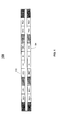
- FIG. 1 depicts an example of a data connector including a single, relatively small-sized data connector having ends that can be swapped, so that an end-user does not need to be concerned with whether the connectors are connected to a host or a slave device. Nor does the end-user have to be concerned with which way the plug is inserted into a receptacle.
- a dual row USB connector may be implemented as depicted at FIG. 1 , there may be implementations where only a portion, such as a single row, of the connector is populated with pins, or galvanic connectors. Moreover, when a single row is populated at the connector at FIG.
- this may affect the ability of devices to detect the orientation of the connector as a first communication control (CC1) pin appears in the first row, and a second communication control pin (CC2) appears in the second row.
- CC1 first communication control
- CC2 second communication control pin
- the CC2 pin 104 may not be active with a pin and the like to provide a connection.
- USB may also include a power negotiation process communicating via a frequency shift key (FSK) modulation scheme over the VBUS path (or line).
- FSK frequency shift key
- This power delivery (PD) negotiation scheme may be too complex for some implementations, especially simpler, lower cost devices and accessories.
- the PD negotiation scheme may also require a VBUS coil, which may add additional and unnecessary direct current (DC) resistance in the charging path.
- DC direct current
- the subject matter disclosed herein may provide, in some example embodiments, two CC pairs for a total of four CC pins.
- the use of four CC pins allows devices to distinguish between a direct plug connection and a rotated or twisted plug connection.
- the two CC pairs may be used as a communication path, such as a path for power delivery negotiation communication to determine initial power roles of USB ports (for example, whether a device is a power provider or a power consumer), although the communication path may be used for other purposes as well.
- This communication path may provide a low rate communication path as an alternative (or in addition to) to other power delivery negotiations communications paths.
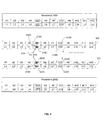
- FIG. 2 depicts an example of a USB connector 205, a cable including at least one wire 210, and another USB connector 220, in accordance with some example embodiments.
- the USB connector 205 may be inserted into a corresponding USB receptacle 299A, and USB connector 220 may be inserted into a corresponding USB receptacle 299B.
- the first USB connector 205 may, in some example embodiments, include two pairs of CC pins 218A-D, such that each row has a CC1 pin and a CC2 pin.
- the first row includes CC1 pin 218A and CC2 pin 218B, and the second row includes CC1 pin 218C and CC2 pin 218D.
- CC1 pins 218A and 218C are coupled 219A, and wire 210 may couple those pins 218A-C to USB connector 220, where CC1 pins 222A and 222C may also be coupled 219B.
- This configuration may ensure that the CC pins are always routed between both connectors 205 and 220 and receptacles 299A-B, when connected. Via the CC-pins one of the CC-lines at the devices are pulled either up or down, so that the change in for example voltage can be detected and thus that location where certain CC pins 218A/218C or 222A/222C are connected.
- the CC pins may also be used for host/slave detection based on the CC-line voltage (or current) change.
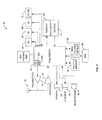
- FIG. 3 depicts an example of a system 300 configured for determining the orientation of the USB connector, in accordance with some example embodiments.
- System 300 may, in some example embodiments, distinguish between connector 205 and connector 205 rotated (or twisted by) 180 degrees, although twists in the wire and/or the other connector may be detected as well.
- the orientation detection also enables detection of the active CC line(s).
- CC1 is active, and can be used, in some example embodiments, to send data and/or receive data.
- stronger (for example, 1 kilo-ohm) pull-up resistors 340A or 340B may be connected at the device 305 to enable low rate communication through the connected CC pin
- the system 300 includes a first device, such as a charger 305 and the like, and a second device, such as a user equipment 320.
- the charger 305 may include a receptacle 299A including two pairs of CC pins 310A-D. However, only one of the rows, such as the top row or the bottom row, may be populated by pins, although both rows may be populated as well.
- CC1 pin 310A and CC2 pin 310B are populated with pins and coupled to device circuitry including pull up resistors 340A-D and orientation detection circuitry 350.
- receptacle 299B, connector 220, wire 210, and connector 205 couple to device 305 including receptacle 299A
- current flows in a certain CC path.
- Current may flow at 360 through CC1 pins 310A, 218A, 218C, wire 210, and so forth.
- This current flow is detected at 362 by orientation detection circuitry 350, which outputs one or more control signals 364A-B indicative of the orientation.
- the output may signal 364A a non-reversed connector.
- orientation detection circuitry 350 which may signal 364B a reversed connector.
- the control signals 364A/364B may be used to switch a stronger pull up resistor 340A or 340B and/or allow communication control (CC) communication to flow through the CC pin which has been detected by the orientation detector 350.
- the stronger pull up may occur after a certain time to allow data to flow via 310A/310C.
- device 320 may include circuitry similar to the circuitry noted above with respect to device 305.
- CC1 pin 380A and CC2 pin 380B may be populated with pins and coupled to the device circuitry including pull down resistors 382A-B and orientation detection circuitry 352.
- receptacle 299A, connector 205, wire 210, and connector 220 couple to device 320 including receptacle 299B, current flows in a certain CC path. In the example of FIG. 3 , current flows at 384A through CC1 pin 380A.
- orientation detection circuitry 352 which detects the orientation and outputs one or more control signals 392A-B to indicate the orientation of the connector 220.
- the output 392B may signal a non-reversed connector. If connector 220 were rotated 180 degrees and inserted into receptacle 299B, current would flow at 384B, which would be detected by orientation detection circuitry 352 and thereby causing a reversed connector control signal 392A.
- the device 320 may be implemented as user equipment, an example of which is described further below with respect to FIG. 7 .
- the device 320 may, in some example embodiments, be configured to pull down CC pins 380A, 380B, and any other CC pins at connector 299B. Although this example refers to pulling down CC pins, the pins may also be pulled up (in which case the other device would pull down the CC pins).
- the device 320 may, in some example embodiments, detect whether the CC pin or pairs of CC pins are connected. When the CC pin or pair of CC pins are detected, device 320 may then initiate communications via the detected CC pin(s) to the other device 205.
- the dual row connector-cable-dual connector assembly 205/210/220 may include two pairs of CC pins (CC) at each end of the cable.
- connector 205 at FIG. 2 includes two pairs of CC pins 218A/C and 218 B/D
- connector 220 includes two pairs of CC pins 222A/C and 222 B/C.
- the CC pins are located on distal portions of the connector 205.
- CC pins 218A/218C are located on the left hand side of connector 205
- CC pins 218B/218D are on the corresponding opposite side.
- CC pins 218A/218C are located at the 5th position moving left to right, while CC pins 218B/218D are located at the 5th position moving right to left, although other placements may be used as well.
- CC pins 218A/218C mirror CC pins 218B/218D, so that twisting connector 205 places CC pins 218A/218C at the same position as CC pins 218B/218D.
- connector 205 may also include CC pin pair 218A/C coupled via a wire 210 to another pin pair 222A/C at connector 220, but CC pin 218B/D may not be connected through to connector 220.
- FIG. 4 depicts an example of a system 400, in accordance with some example embodiments.
- System 400 is similar to system 300 in some respects but includes a device 405 having an integrated (or captive) cable 410 and connector 415.
- the device 405 may be implemented as a charger or other accessory, which includes an integrated/captive cable 410 and connector 415.
- the connector 415 may be implemented in the same manner as noted above with respect to 299A. When this is the case, connector 415 includes two pairs of CC pins 490A-D.
- device 405, unlike device 305, may not include the orientation detection circuitry 350 described with respect to FIG. 3 . In the example of FIG.
- device/charger 405 pulls up both pairs of CC lines, which is detected by device 320 at the orientation detection circuitry 352.
- the AND function may be used to detect whether the connector 415 orientation (for example, reversed or not), and this signal may be used to enable communications through one of the CC pins.
- FIG. 5 depicts an example of a system 500, in accordance with some example embodiments.
- System 500 is similar to system 400 in some respects but adds a micro USB configuration. Specifically, a micro USB plug 505, micro USB receptacle adapter 510 is added to interface with connector 515, which is the same or similar to connector 205, 299A, 415, and the like.
- FIG. 6 depicts a process for communication control via a universal serial bus, in accordance with some example embodiments. The description of FIG. 6 also refers to FIGs. 2 and 3 .
- a first device is coupled to a second device, in accordance with some example embodiments.
- a first device such as device 305 may include two pairs of CC pins as depicted at FIGs. 2 and 3 .
- the CC pins may both be pulled up by pull up resistors.
- the first device 305 may be coupled to the second device 320 via connector-cable-connector assembly 205/210/220.
- the cable may however not connect both pairs of CC pins, but instead have a single wire 210 connecting a single pair of CC pins.
- the CC pins at device 320 may be pulled down.
- a current flow is detected at one the CC pins, in accordance with some example embodiments.
- orientation detection circuit 352 may detect a current flow associated with the CC pair 310A/C coupling via wire 210 to CC pair 380A/C.
- device 320 may recognize the orientation of the connector and/or the CC pin(s) which are active.
- CC pins 380A/C are active, so device 320 may recognize that CC pins 380A/C are active, but CC pins 380B/D are not (by virtual of a lack of connection via connector-cable-connector assembly 205/210/220).
- devices 305 and 320 may access the detected CC pin for communication control (or other purposed) between device 305 and 320, in accordance with some example embodiments.
- device 305 may couple data, such as communication control signaling, to the detected CC pin(s), such as 310A.
- Device 320 may couple data, such as communication control signaling, to CC pin detected at 610 (for example, CC pin 380A). This coupling may be under the control of circuitry 350 and one or more of switches 313A-D.
- FIG. 7 illustrates a block diagram of an apparatus 10, which can be configured as user equipment, in accordance with some example embodiments.
- the apparatus 10 may include USB interface 614A, which may include one or more aspects of the systems and methods disclosed herein including connectors, pull up resistors, pull down resistors, detection circuitry, and the like.
- the apparatus 10 may include at least one antenna 12 in communication with a transmitter 14 and a receiver 16. Alternatively transmit and receive antennas may be separate.
- the apparatus 10 may also include a processor 20 configured to provide signals to and receive signals from the transmitter and receiver, respectively, and to control the functioning of the apparatus.
- Processor 20 may be configured to control the functioning of the transmitter and receiver by effecting control signaling via electrical leads to the transmitter and receiver.
- processor 20 may be configured to control other elements of apparatus 10 by effecting control signaling via electrical leads connecting processor 20 to the other elements, such as for example a display or a memory.
- the processor 20 may, for example, be embodied in a variety of ways including circuitry, at least one processing core, one or more microprocessors with accompanying digital signal processor(s), one or more processor(s) without an accompanying digital signal processor, one or more coprocessors, one or more multi-core processors, one or more controllers, processing circuitry, one or more computers, various other processing elements including integrated circuits (for example, an application specific integrated circuit (ASIC), a field programmable gate array (FPGA), and/or the like), or some combination thereof.
- Apparatus 10 may include a location processor and/or an interface to obtain location information, such as positioning and/or navigation information. Accordingly, although illustrated in FIG. 7 as a single processor, in some example embodiments the processor 20 may comprise a plurality of processors or processing cores.
- Signals sent and received by the processor 20 may include signaling information in accordance with an air interface standard of an applicable cellular system, and/or any number of different wireline or wireless networking techniques, comprising but not limited to Wi-Fi, wireless local access network (WLAN) techniques, such as for example, Institute of Electrical and Electronics Engineers (IEEE) 802.11, 802.16, and/or the like.
- these signals may include speech data, user generated data, user requested data, and/or the like.
- the apparatus 10 may be capable of operating with one or more air interface standards, communication protocols, modulation types, access types, and/or the like.
- the apparatus 10 and/or a cellular modem therein may be capable of operating in accordance with various first generation (1 G) communication protocols, second generation (2G or 2.5G) communication protocols, third-generation (3G) communication protocols, fourth-generation (4G) communication protocols, Internet Protocol Multimedia Subsystem (IMS) communication protocols (for example, session initiation protocol (SIP) and/or the like.
- IMS Internet Protocol Multimedia Subsystem
- the apparatus 10 may be capable of operating in accordance with 2G wireless communication protocols IS-136, Time Division Multiple Access TDMA, Global System for Mobile communications, GSM, IS-95, Code Division Multiple Access, CDMA, and/or the like.
- the apparatus 10 may be capable of operating in accordance with 2.5G wireless communication protocols General Packet Radio Service (GPRS), Enhanced Data GSM Environment (EDGE), and/or the like. Further, for example, the apparatus 10 may be capable of operating in accordance with 3G wireless communication protocols, such as for example, Universal Mobile Telecommunications System (UMTS), Code Division Multiple Access 2000 (CDMA2000), Wideband Code Division Multiple Access (WCDMA), Time Division-Synchronous Code Division Multiple Access (TD-SCDMA), and/or the like. The apparatus 10 may be additionally capable of operating in accordance with 3.9G wireless communication protocols, such as for example, Long Term Evolution (LTE), Evolved Universal Terrestrial Radio Access Network (E-UTRAN), and/or the like. Additionally, for example, the apparatus 10 may be capable of operating in accordance with 4G wireless communication protocols, such as for example LTE Advanced and/or the like as well as similar wireless communication protocols that may be subsequently developed.
- GPRS General Packet Radio Service
- EDGE Enhanced Data GSM Environment
- the processor 20 may include circuitry for implementing audio/video and logic functions of apparatus 10.
- the processor 20 may comprise a digital signal processor device, a microprocessor device, an analog-to-digital converter, a digital-to-analog converter, and/or the like. Control and signal processing functions of the apparatus 10 may be allocated between these devices according to their respective capabilities.
- the processor 20 may additionally comprise an internal voice coder (VC) 20a, an internal data modem (DM) 20b, and/or the like.
- the processor 20 may include functionality to operate one or more software programs, which may be stored in memory. In general, processor 20 and stored software instructions may be configured to cause apparatus 10 to perform actions.
- processor 20 may be capable of operating a connectivity program, such as for example, a web browser.
- the connectivity program may allow the apparatus 10 to transmit and receive web content, such as for example location-based content, according to a protocol, such as for example, wireless application protocol, WAP, hypertext transfer protocol, HTTP, and/or the like.
- Apparatus 10 may also comprise a user interface including, for example, an earphone or speaker 24, a ringer 22, a microphone 26, a display 28, a user input interface, and/or the like, which may be operationally coupled to the processor 20.
- the display 28 may, as noted above, include a touch sensitive display, where a user may touch and/or gesture to make selections, enter values, and/or the like.
- the processor 20 may also include user interface circuitry configured to control at least some functions of one or more elements of the user interface, such as for example, the speaker 24, the ringer 22, the microphone 26, the display 28, and/or the like.
- the processor 20 and/or user interface circuitry comprising the processor 20 may be configured to control one or more functions of one or more elements of the user interface through computer program instructions, for example, software and/or firmware, stored on a memory accessible to the processor 20, for example, volatile memory 40, non-volatile memory 42, and/or the like.
- the apparatus 10 may include a battery for powering various circuits related to the mobile terminal, for example, a circuit to provide mechanical vibration as a detectable output.
- the user input interface may comprise devices allowing the apparatus 20 to receive data, such as for example, a keypad 30 (which can be a virtual keyboard presented on display 28 or an externally coupled keyboard) and/or other input devices.
- the apparatus 10 may include a short-range radio frequency (RF) transceiver and/or interrogator 64, so data may be shared with and/or obtained from electronic devices in accordance with RF techniques.
- the apparatus 10 may include other short-range transceivers, such as for example an infrared (IR) transceiver 66, a Bluetooth (BT) transceiver 68 operating using Bluetooth wireless technology, a wireless universal serial bus (USB) transceiver 70, and/or the like.
- the Bluetooth transceiver 68 may be capable of operating according to low power or ultra-low power Bluetooth technology, for example, Wibree, radio standards.
- the apparatus 10 and, in particular, the short-range transceiver may be capable of transmitting data to and/or receiving data from electronic devices within a proximity of the apparatus, such as for example within 10 meters.
- the apparatus 10 including the WiFi or wireless local area networking modem may also be capable of transmitting and/or receiving data from electronic devices according to various wireless networking techniques, including 6LoWpan, Wi-Fi, Wi-Fi low power, WLAN techniques such as for example IEEE 802.11 techniques, IEEE 802.15 techniques, IEEE 802.16 techniques, and/or the like.
- the apparatus 10 may comprise memory, such as for example, a subscriber identity module (SIM) 38, a removable user identity module (R-UIM), and/or the like, which may store information elements related to a mobile subscriber. In addition to the SIM, the apparatus 10 may include other removable and/or fixed memory.
- the apparatus 10 may include volatile memory 40 and/or non-volatile memory 42.
- volatile memory 40 may include Random Access Memory (RAM) including dynamic and/or static RAM, on-chip or off-chip cache memory, and/or the like.
- RAM Random Access Memory
- Non-volatile memory 42 which may be embedded and/or removable, may include, for example, read-only memory, flash memory, magnetic storage devices, for example, hard disks, floppy disk drives, magnetic tape, optical disc drives and/or media, non-volatile random access memory (NVRAM), and/or the like. Like volatile memory 40, non-volatile memory 42 may include a cache area for temporary storage of data. At least part of the volatile and/or non-volatile memory may be embedded in processor 20. The memories may store one or more software programs instructions, pieces of information, data, and/or the like which may be used by the apparatus for performing functions of the user equipment/mobile terminal.
- NVRAM non-volatile random access memory
- the memories may comprise an identifier, such as for example an international mobile equipment identification (IMEI) code, capable of uniquely identifying apparatus 10.
- the functions may include one or more of the operations disclosed herein with respect to the user equipment, such as for example the functions disclosed at process 200.
- the memories may comprise an identifier, such as for example, an international mobile equipment identification (IMEI) code, capable of uniquely identifying apparatus 10.
- the processor 20 may be configured using computer code stored at memory 40 and/or 42 to perform or cause process 600 or other operations disclosed herein with respect to the devices at FIGs. 3-5 , and/or the like as disclosed herein.
- Some of the embodiments disclosed herein may be implemented in software, hardware, application logic, or a combination of software, hardware, and application logic.
- the software, application logic, and/or hardware may reside on memory 40, the control apparatus 20, or electronic components, for example.
- the application logic, software or an instruction set is maintained on any one of various conventional computer-readable media.
- a "computer-readable medium" may be any non-transitory media that can contain, store, communicate, propagate or transport the instructions for use by or in connection with an instruction execution system, apparatus, or device, such as for example a computer or data processor circuitry, with examples depicted at FIGs. 6 (for example, process 600 or other operations disclosed herein with respect to the devices at FIGs. 3-5 ).
- a computer-readable medium may comprise a non-transitory computer-readable storage medium that may be any media that can contain or store the instructions for use by or in connection with an instruction execution system, apparatus, or device, such as for example a computer.
- some of the embodiments disclosed herein include computer programs configured to cause and/or provide methods as disclosed herein (see, for example, process 600 and/or the like).
- a technical effect of one or more of the example embodiments disclosed herein is reduced complexity for some devices by eliminating the need to populate both the top and bottom rows of the connector and enabling communications via a detected communication control path.
- a connector may be a male connector (in which case it may be referred to as a plug) or a female connector (in which case it may also be referred to as a receptacle).
Landscapes
- Engineering & Computer Science (AREA)
- Theoretical Computer Science (AREA)
- General Engineering & Computer Science (AREA)
- Physics & Mathematics (AREA)
- General Physics & Mathematics (AREA)
- Computer Hardware Design (AREA)
- Software Systems (AREA)
- Details Of Connecting Devices For Male And Female Coupling (AREA)
- Microelectronics & Electronic Packaging (AREA)
- Information Transfer Systems (AREA)
Abstract
Description
- The subject matter described herein relates to connectors and/or cables associated with the Universal Serial Bus (USB).
- Physical connectors, such as the connector used with the Universal Serial Bus (USB), can be used to couple devices. USB standards define physical and electrical aspects of USB. Examples of those standards include Universal Serial Bus 3.1 Specification, Universal Serial Bus 3.0 Specification, and any additions, revisions, and updates thereto.
- Methods and apparatus, including computer program products, are provided for communications control in a dual row connector.
- In some example embodiments, there is provided an apparatus. The apparatus may include a first data connector including a pair of communication control pins and another pair of communication control pins, wherein the pair further comprises a first communication control pin located at a first row of the first data connector and a second communication control pin located at a second row of the data connector, wherein the other pair further comprises a third communication control pin located at the first row of the first data connector and a fourth communication control pin located at the second row of the first data connector.
- In some variations, one or more of the features disclosed herein including the following features can optionally be included in any feasible combination. The apparatus may further include a second data connector including a first pair of communication control pins and a second pair of communication control pins, wherein the first pair further comprises a fifth communication control pin located at a top row of the second data connector and a sixth communication control pin located at a bottom row of the second data connector, wherein the second pair further comprises a sixth communication control pin located at the top row of the second data connector and a eighth communication control pin located at the bottom row of the second data connector; and a cable including at least one wire coupling the first communication control pin and the fifth communication control pin. The first communication control pin and the second communication control pin may be coupled at the first data connector, and wherein the fifth communication control pin and the sixth communication control pin may be coupled at the second data connector. The first communication control pin and the second communication control pin may be coupled at the first data connector. The first data connector may include a universal serial bus connector.
- Moreover, there is provided in some example embodiments an apparatus including a data connector including a first communication control pin and a second communication control pin, wherein the first communication control pin and the second communication control pin are pulled up by at least one pull-up resistor; detection circuitry to detect one communication control pin of the first and the second communication control pins by at least detecting a current flow caused by at least the pull-up when coupled to the data connector and another device; and communication circuitry coupled to the one communication control pin detected by the detection circuitry and configured to communicate according to a communication protocol.
- In some variations, one or more of the features disclosed herein including the following features can optionally be included in any feasible combination. The data connector may include a first row including the first communication control pin and the second communication control pin, and a second row including a third communication control pin and a fourth communication control pin. The apparatus may include at least another pull-up, wherein the other pull-up may be configured to be connected to the one communication pin when detected by the detection circuitry. The other pull-up may include another pull-up resistor comprising a higher resistance than the at least one pull-up resistor. The communication circuitry may be configured to communicate according to another communication protocol, when the detection circuitry detects a current flow both in the first communication control pin and the second communication control pin. The first communication control pin may be coupled to the third communication control pin and wherein the second communication control pin may be coupled to the fourth communication control pin. The first data connector may include a universal serial bus connector.
- Furthermore, there is provided in some example embodiments an apparatus including a data connector including a first communication control pin and a second communication control pin, wherein the first communication control pin and the second communication control pin are pulled down by at least one pull-down resistor; detection circuitry configured to detect one communication control pin of the first and the second communication control pins by at least detecting a current flow caused by at least the pull down when coupled to the data connector and another device; and communication circuitry coupled to the one communication control pin detected by the detection circuitry and configured to communicate according to a communication protocol.
- In some variations, one or more of the features disclosed herein including the following features can optionally be included in any feasible combination. The data connector may include a first row including the first communication control pin and the second communication control pin, and a second row including a third communication control pin and a fourth communication control pin. The communication circuitry may be configured to communicate according to another communication protocol, when the detection circuitry detects a current flow both in the first communication control pin and the second communication control pin. The first communication control pin may be coupled to the third communication control pin and wherein the second communication control pin may be coupled to the fourth communication control pin.
- The above-noted aspects and features may be implemented in systems, apparatus, methods, and/or articles depending on the desired configuration. The details of one or more variations of the subject matter described herein are set forth in the accompanying drawings and the description below. Features and advantages of the subject matter described herein will be apparent from the description and drawings, and from the claims.
- In the drawings,
-
FIG. 1 depicts an example of a data connector; -
FIG. 2 depicts examples of data connectors and interfaces having two pairs of communication control pins, in accordance with some exemplary embodiments; -
FIG. 3 depicts an example of a system in which the connectors and interfaces ofFIG.2 may be used in accordance with some exemplary embodiments; -
FIGs. 4-5 depict examples of systems including two pairs of communication control pins, in accordance with some example embodiments; -
FIG. 6 depicts an example process for depicting at least one of the communication control pin, in accordance with some exemplary embodiments; and -
FIG. 7 depicts an example of an apparatus, in accordance with some exemplary embodiments. - Like labels are used to refer to same or similar items in the drawings.
-
FIG. 1 depicts an example of a data connector including a single, relatively small-sized data connector having ends that can be swapped, so that an end-user does not need to be concerned with whether the connectors are connected to a host or a slave device. Nor does the end-user have to be concerned with which way the plug is inserted into a receptacle. Although a dual row USB connector may be implemented as depicted atFIG. 1 , there may be implementations where only a portion, such as a single row, of the connector is populated with pins, or galvanic connectors. Moreover, when a single row is populated at the connector atFIG. 1 , this may affect the ability of devices to detect the orientation of the connector as a first communication control (CC1) pin appears in the first row, and a second communication control pin (CC2) appears in the second row. As such, if only a top row is populated and the connector is reoriented by 180 degrees (for example, rotated or twisted), theCC2 pin 104 may not be active with a pin and the like to provide a connection. - Some implementations of USB may also include a power negotiation process communicating via a frequency shift key (FSK) modulation scheme over the VBUS path (or line). This power delivery (PD) negotiation scheme may be too complex for some implementations, especially simpler, lower cost devices and accessories. Moreover, the PD negotiation scheme may also require a VBUS coil, which may add additional and unnecessary direct current (DC) resistance in the charging path.
- The subject matter disclosed herein may provide, in some example embodiments, two CC pairs for a total of four CC pins. The use of four CC pins allows devices to distinguish between a direct plug connection and a rotated or twisted plug connection. Moreover, the two CC pairs may be used as a communication path, such as a path for power delivery negotiation communication to determine initial power roles of USB ports (for example, whether a device is a power provider or a power consumer), although the communication path may be used for other purposes as well. This communication path may provide a low rate communication path as an alternative (or in addition to) to other power delivery negotiations communications paths.
-
FIG. 2 depicts an example of aUSB connector 205, a cable including at least onewire 210, and anotherUSB connector 220, in accordance with some example embodiments. TheUSB connector 205 may be inserted into acorresponding USB receptacle 299A, andUSB connector 220 may be inserted into acorresponding USB receptacle 299B. - The
first USB connector 205 may, in some example embodiments, include two pairs ofCC pins 218A-D, such that each row has a CC1 pin and a CC2 pin. The first row includesCC1 pin 218A andCC2 pin 218B, and the second row includesCC1 pin 218C andCC2 pin 218D. In the example ofFIG. 2 ,CC1 pins wire 210 may couple thosepins 218A-C toUSB connector 220, whereCC1 pins connectors receptacles 299A-B, when connected. Via the CC-pins one of the CC-lines at the devices are pulled either up or down, so that the change in for example voltage can be detected and thus that location wherecertain CC pins 218A/218C or 222A/222C are connected. The CC pins may also be used for host/slave detection based on the CC-line voltage (or current) change. -
FIG. 3 depicts an example of asystem 300 configured for determining the orientation of the USB connector, in accordance with some example embodiments.System 300 may, in some example embodiments, distinguish betweenconnector 205 andconnector 205 rotated (or twisted by) 180 degrees, although twists in the wire and/or the other connector may be detected as well. The orientation detection also enables detection of the active CC line(s). In the example ofFIG. 3 , CC1 is active, and can be used, in some example embodiments, to send data and/or receive data. For example, after detecting connector orientation, stronger (for example, 1 kilo-ohm) pull-upresistors device 305 to enable low rate communication through the connected CC pin - The
system 300 includes a first device, such as acharger 305 and the like, and a second device, such as auser equipment 320. Thecharger 305 may include areceptacle 299A including two pairs of CC pins 310A-D. However, only one of the rows, such as the top row or the bottom row, may be populated by pins, although both rows may be populated as well. In the example ofFIG. 3 ,CC1 pin 310A andCC2 pin 310B are populated with pins and coupled to device circuitry including pull upresistors 340A-D andorientation detection circuitry 350. Whendevice 320,receptacle 299B,connector 220,wire 210, andconnector 205 couple todevice 305 includingreceptacle 299A, current flows in a certain CC path. Current may flow at 360 through CC1 pins 310A, 218A, 218C,wire 210, and so forth. This current flow is detected at 362 byorientation detection circuitry 350, which outputs one ormore control signals 364A-B indicative of the orientation. In the example ofFIG. 3 , the output may signal 364A a non-reversed connector. However, if connector 205A were rotated 180 degrees and inserted intoreceptacle 299A, current would instead flow at 370 through CC2 pins 310B, 218A/218C (which has been rotated), and so forth. This current flow is detected at 372 byorientation detection circuitry 350, which may signal 364B a reversed connector. - The control signals 364A/364B may be used to switch a stronger pull up
resistor orientation detector 350. The stronger pull up may occur after a certain time to allow data to flow via 310A/310C. - In the example of
FIG. 3 ,device 320 may include circuitry similar to the circuitry noted above with respect todevice 305. For example,CC1 pin 380A andCC2 pin 380B may be populated with pins and coupled to the device circuitry including pull downresistors 382A-B andorientation detection circuitry 352. Whendevice 305,receptacle 299A,connector 205,wire 210, andconnector 220 couple todevice 320 includingreceptacle 299B, current flows in a certain CC path. In the example ofFIG. 3 , current flows at 384A throughCC1 pin 380A. This current flow is detected byorientation detection circuitry 352, which detects the orientation and outputs one ormore control signals 392A-B to indicate the orientation of theconnector 220. In the example ofFIG. 3 , theoutput 392B may signal a non-reversed connector. Ifconnector 220 were rotated 180 degrees and inserted intoreceptacle 299B, current would flow at 384B, which would be detected byorientation detection circuitry 352 and thereby causing a reversedconnector control signal 392A. - In some example embodiments, the
device 320 may be implemented as user equipment, an example of which is described further below with respect toFIG. 7 . Thedevice 320 may, in some example embodiments, be configured to pull down CC pins 380A, 380B, and any other CC pins atconnector 299B. Although this example refers to pulling down CC pins, the pins may also be pulled up (in which case the other device would pull down the CC pins). Thedevice 320 may, in some example embodiments, detect whether the CC pin or pairs of CC pins are connected. When the CC pin or pair of CC pins are detected,device 320 may then initiate communications via the detected CC pin(s) to theother device 205. - In some example embodiments, the dual row connector-cable-
dual connector assembly 205/210/220 may include two pairs of CC pins (CC) at each end of the cable. For example,connector 205 atFIG. 2 includes two pairs of CC pins 218A/C and 218 B/D, andconnector 220 includes two pairs of CC pins 222A/C and 222 B/C. The CC pins are located on distal portions of theconnector 205. For example, CC pins 218A/218C are located on the left hand side ofconnector 205, and CC pins 218B/218D are on the corresponding opposite side. Indeed, CC pins 218A/218C are located at the 5th position moving left to right, while CC pins 218B/218D are located at the 5th position moving right to left, although other placements may be used as well. As a consequence, CC pins 218A/218C mirror CC pins 218B/218D, so that twistingconnector 205 places CC pins 218A/218C at the same position as CC pins 218B/218D. Moreover,connector 205 may also includeCC pin pair 218A/C coupled via awire 210 to anotherpin pair 222A/C atconnector 220, butCC pin 218B/D may not be connected through toconnector 220. -
FIG. 4 depicts an example of asystem 400, in accordance with some example embodiments.System 400 is similar tosystem 300 in some respects but includes adevice 405 having an integrated (or captive)cable 410 andconnector 415. For example, thedevice 405 may be implemented as a charger or other accessory, which includes an integrated/captive cable 410 andconnector 415. Theconnector 415 may be implemented in the same manner as noted above with respect to 299A. When this is the case,connector 415 includes two pairs of CC pins 490A-D. Moreover,device 405, unlikedevice 305, may not include theorientation detection circuitry 350 described with respect toFIG. 3 . In the example ofFIG. 4 , after the orientation is detected, device/charger 405 pulls up both pairs of CC lines, which is detected bydevice 320 at theorientation detection circuitry 352. For example, the AND function may be used to detect whether theconnector 415 orientation (for example, reversed or not), and this signal may be used to enable communications through one of the CC pins. -
FIG. 5 depicts an example of asystem 500, in accordance with some example embodiments.System 500 is similar tosystem 400 in some respects but adds a micro USB configuration. Specifically, amicro USB plug 505, microUSB receptacle adapter 510 is added to interface with connector 515, which is the same or similar toconnector -
FIG. 6 depicts a process for communication control via a universal serial bus, in accordance with some example embodiments. The description ofFIG. 6 also refers toFIGs. 2 and3 . - At 605, a first device is coupled to a second device, in accordance with some example embodiments. For example, a first device, such as
device 305 may include two pairs of CC pins as depicted atFIGs. 2 and3 . Moreover, the CC pins may both be pulled up by pull up resistors. Thefirst device 305 may be coupled to thesecond device 320 via connector-cable-connector assembly 205/210/220. Furthermore, the cable may however not connect both pairs of CC pins, but instead have asingle wire 210 connecting a single pair of CC pins. The CC pins atdevice 320 may be pulled down. - At 610, a current flow is detected at one the CC pins, in accordance with some example embodiments. For example,
orientation detection circuit 352 may detect a current flow associated with theCC pair 310A/C coupling viawire 210 toCC pair 380A/C. As such,device 320 may recognize the orientation of the connector and/or the CC pin(s) which are active. In the example ofFIG. 3 , CC pins 380A/C are active, sodevice 320 may recognize that CC pins 380A/C are active, but CC pins 380B/D are not (by virtual of a lack of connection via connector-cable-connector assembly 205/210/220). - At 620,
devices device FIG. 3 ,device 305 may couple data, such as communication control signaling, to the detected CC pin(s), such as 310A.Device 320 may couple data, such as communication control signaling, to CC pin detected at 610 (for example,CC pin 380A). This coupling may be under the control ofcircuitry 350 and one or more ofswitches 313A-D. -
FIG. 7 illustrates a block diagram of anapparatus 10, which can be configured as user equipment, in accordance with some example embodiments. Theapparatus 10 may include USB interface 614A, which may include one or more aspects of the systems and methods disclosed herein including connectors, pull up resistors, pull down resistors, detection circuitry, and the like. - The
apparatus 10 may include at least oneantenna 12 in communication with atransmitter 14 and areceiver 16. Alternatively transmit and receive antennas may be separate. - The
apparatus 10 may also include aprocessor 20 configured to provide signals to and receive signals from the transmitter and receiver, respectively, and to control the functioning of the apparatus.Processor 20 may be configured to control the functioning of the transmitter and receiver by effecting control signaling via electrical leads to the transmitter and receiver. Likewiseprocessor 20 may be configured to control other elements ofapparatus 10 by effecting control signaling via electricalleads connecting processor 20 to the other elements, such as for example a display or a memory. Theprocessor 20 may, for example, be embodied in a variety of ways including circuitry, at least one processing core, one or more microprocessors with accompanying digital signal processor(s), one or more processor(s) without an accompanying digital signal processor, one or more coprocessors, one or more multi-core processors, one or more controllers, processing circuitry, one or more computers, various other processing elements including integrated circuits (for example, an application specific integrated circuit (ASIC), a field programmable gate array (FPGA), and/or the like), or some combination thereof.Apparatus 10 may include a location processor and/or an interface to obtain location information, such as positioning and/or navigation information. Accordingly, although illustrated inFIG. 7 as a single processor, in some example embodiments theprocessor 20 may comprise a plurality of processors or processing cores. - Signals sent and received by the
processor 20 may include signaling information in accordance with an air interface standard of an applicable cellular system, and/or any number of different wireline or wireless networking techniques, comprising but not limited to Wi-Fi, wireless local access network (WLAN) techniques, such as for example, Institute of Electrical and Electronics Engineers (IEEE) 802.11, 802.16, and/or the like. In addition, these signals may include speech data, user generated data, user requested data, and/or the like. - The
apparatus 10 may be capable of operating with one or more air interface standards, communication protocols, modulation types, access types, and/or the like. For example, theapparatus 10 and/or a cellular modem therein may be capable of operating in accordance with various first generation (1 G) communication protocols, second generation (2G or 2.5G) communication protocols, third-generation (3G) communication protocols, fourth-generation (4G) communication protocols, Internet Protocol Multimedia Subsystem (IMS) communication protocols (for example, session initiation protocol (SIP) and/or the like. For example, theapparatus 10 may be capable of operating in accordance with 2G wireless communication protocols IS-136, Time Division Multiple Access TDMA, Global System for Mobile communications, GSM, IS-95, Code Division Multiple Access, CDMA, and/or the like. In addition, for example, theapparatus 10 may be capable of operating in accordance with 2.5G wireless communication protocols General Packet Radio Service (GPRS), Enhanced Data GSM Environment (EDGE), and/or the like. Further, for example, theapparatus 10 may be capable of operating in accordance with 3G wireless communication protocols, such as for example, Universal Mobile Telecommunications System (UMTS), Code Division Multiple Access 2000 (CDMA2000), Wideband Code Division Multiple Access (WCDMA), Time Division-Synchronous Code Division Multiple Access (TD-SCDMA), and/or the like. Theapparatus 10 may be additionally capable of operating in accordance with 3.9G wireless communication protocols, such as for example, Long Term Evolution (LTE), Evolved Universal Terrestrial Radio Access Network (E-UTRAN), and/or the like. Additionally, for example, theapparatus 10 may be capable of operating in accordance with 4G wireless communication protocols, such as for example LTE Advanced and/or the like as well as similar wireless communication protocols that may be subsequently developed. - It is understood that the
processor 20 may include circuitry for implementing audio/video and logic functions ofapparatus 10. For example, theprocessor 20 may comprise a digital signal processor device, a microprocessor device, an analog-to-digital converter, a digital-to-analog converter, and/or the like. Control and signal processing functions of theapparatus 10 may be allocated between these devices according to their respective capabilities. Theprocessor 20 may additionally comprise an internal voice coder (VC) 20a, an internal data modem (DM) 20b, and/or the like. Further, theprocessor 20 may include functionality to operate one or more software programs, which may be stored in memory. In general,processor 20 and stored software instructions may be configured to causeapparatus 10 to perform actions. For example,processor 20 may be capable of operating a connectivity program, such as for example, a web browser. The connectivity program may allow theapparatus 10 to transmit and receive web content, such as for example location-based content, according to a protocol, such as for example, wireless application protocol, WAP, hypertext transfer protocol, HTTP, and/or the like. -
Apparatus 10 may also comprise a user interface including, for example, an earphone orspeaker 24, aringer 22, amicrophone 26, adisplay 28, a user input interface, and/or the like, which may be operationally coupled to theprocessor 20. Thedisplay 28 may, as noted above, include a touch sensitive display, where a user may touch and/or gesture to make selections, enter values, and/or the like. Theprocessor 20 may also include user interface circuitry configured to control at least some functions of one or more elements of the user interface, such as for example, thespeaker 24, theringer 22, themicrophone 26, thedisplay 28, and/or the like. Theprocessor 20 and/or user interface circuitry comprising theprocessor 20 may be configured to control one or more functions of one or more elements of the user interface through computer program instructions, for example, software and/or firmware, stored on a memory accessible to theprocessor 20, for example,volatile memory 40,non-volatile memory 42, and/or the like. Theapparatus 10 may include a battery for powering various circuits related to the mobile terminal, for example, a circuit to provide mechanical vibration as a detectable output. The user input interface may comprise devices allowing theapparatus 20 to receive data, such as for example, a keypad 30 (which can be a virtual keyboard presented ondisplay 28 or an externally coupled keyboard) and/or other input devices. - Moreover, the
apparatus 10 may include a short-range radio frequency (RF) transceiver and/orinterrogator 64, so data may be shared with and/or obtained from electronic devices in accordance with RF techniques. Theapparatus 10 may include other short-range transceivers, such as for example an infrared (IR)transceiver 66, a Bluetooth (BT)transceiver 68 operating using Bluetooth wireless technology, a wireless universal serial bus (USB)transceiver 70, and/or the like. TheBluetooth transceiver 68 may be capable of operating according to low power or ultra-low power Bluetooth technology, for example, Wibree, radio standards. In this regard, theapparatus 10 and, in particular, the short-range transceiver may be capable of transmitting data to and/or receiving data from electronic devices within a proximity of the apparatus, such as for example within 10 meters. Theapparatus 10 including the WiFi or wireless local area networking modem may also be capable of transmitting and/or receiving data from electronic devices according to various wireless networking techniques, including 6LoWpan, Wi-Fi, Wi-Fi low power, WLAN techniques such as for example IEEE 802.11 techniques, IEEE 802.15 techniques, IEEE 802.16 techniques, and/or the like. - The
apparatus 10 may comprise memory, such as for example, a subscriber identity module (SIM) 38, a removable user identity module (R-UIM), and/or the like, which may store information elements related to a mobile subscriber. In addition to the SIM, theapparatus 10 may include other removable and/or fixed memory. Theapparatus 10 may includevolatile memory 40 and/ornon-volatile memory 42. For example,volatile memory 40 may include Random Access Memory (RAM) including dynamic and/or static RAM, on-chip or off-chip cache memory, and/or the like.Non-volatile memory 42, which may be embedded and/or removable, may include, for example, read-only memory, flash memory, magnetic storage devices, for example, hard disks, floppy disk drives, magnetic tape, optical disc drives and/or media, non-volatile random access memory (NVRAM), and/or the like. Likevolatile memory 40,non-volatile memory 42 may include a cache area for temporary storage of data. At least part of the volatile and/or non-volatile memory may be embedded inprocessor 20. The memories may store one or more software programs instructions, pieces of information, data, and/or the like which may be used by the apparatus for performing functions of the user equipment/mobile terminal. The memories may comprise an identifier, such as for example an international mobile equipment identification (IMEI) code, capable of uniquely identifyingapparatus 10. The functions may include one or more of the operations disclosed herein with respect to the user equipment, such as for example the functions disclosed at process 200. The memories may comprise an identifier, such as for example, an international mobile equipment identification (IMEI) code, capable of uniquely identifyingapparatus 10. In the example embodiment, theprocessor 20 may be configured using computer code stored atmemory 40 and/or 42 to perform orcause process 600 or other operations disclosed herein with respect to the devices atFIGs. 3-5 , and/or the like as disclosed herein. - Some of the embodiments disclosed herein may be implemented in software, hardware, application logic, or a combination of software, hardware, and application logic. The software, application logic, and/or hardware may reside on
memory 40, thecontrol apparatus 20, or electronic components, for example. In some example embodiment, the application logic, software or an instruction set is maintained on any one of various conventional computer-readable media. In the context of this document, a "computer-readable medium" may be any non-transitory media that can contain, store, communicate, propagate or transport the instructions for use by or in connection with an instruction execution system, apparatus, or device, such as for example a computer or data processor circuitry, with examples depicted atFIGs. 6 (for example,process 600 or other operations disclosed herein with respect to the devices atFIGs. 3-5 ). A computer-readable medium may comprise a non-transitory computer-readable storage medium that may be any media that can contain or store the instructions for use by or in connection with an instruction execution system, apparatus, or device, such as for example a computer. Furthermore, some of the embodiments disclosed herein include computer programs configured to cause and/or provide methods as disclosed herein (see, for example,process 600 and/or the like). - Without in any way limiting the scope, interpretation, or application of the claims appearing below, a technical effect of one or more of the example embodiments disclosed herein is reduced complexity for some devices by eliminating the need to populate both the top and bottom rows of the connector and enabling communications via a detected communication control path.
- If desired, the different functions discussed herein may be performed in a different order and/or concurrently with each other. Furthermore, if desired, one or more of the above-described functions may be optional or may be combined. Although various aspects of the invention are set out in the independent claims, other aspects of the invention comprise other combinations of features from the described embodiments and/or the dependent claims with the features of the independent claims, and not solely the combinations explicitly set out in the claims. It is also noted herein that while the above describes example embodiments, these descriptions should not be viewed in a limiting sense. Rather, there are several variations and modifications that may be made without departing from the scope of the present invention as defined in the appended claims. Other embodiments may be within the scope of the following claims. The term "based on" includes "based on at least." As used herein, a connector may be a male connector (in which case it may be referred to as a plug) or a female connector (in which case it may also be referred to as a receptacle).
Claims (11)
- An apparatus comprising:a data connector including a first communication control pin and a second communication control pin, wherein the first communication control pin and the second communication control pin are pulled up by at least one pull-up resistor;detection circuitry to detect one communication control pin of the first and the second communication control pins by at least detecting a current flow or a change in voltage caused by at least the pull-up when coupled to the data connector and another device; and communication circuitry coupled to the one communication control pin detected by the detection circuitry and configured to communicate according to a communication protocol.
- The apparatus of claim 1, further comprising;
at least another pull-up, wherein the other pull-up is configured to be connected to the one communication pin when detected by the detection circuitry. - The apparatus of claim 2, wherein the other pull-up comprises another pull-up resistor comprising a higher resistance than the at least one pull-up resistor.
- The apparatus of any of claims 1 to 3, wherein the communication circuitry is configured to communicate according to another communication protocol, when the detection circuitry detects a current flow or a change in voltage both in the first communication control pin and the second communication control pin.
- The apparatus of any of claims 1 to 4, wherein the first data connector comprises a universal serial bus connector.
- An apparatus comprising:a data connector including a first communication control pin and a second communication control pin, wherein the first communication control pin and the second communication control pin are pulled down by at least one pull-down resistor;detection circuitry configured to detect one communication control pin of the first and the second communication control pins by at least detecting a current flow or a change in voltage caused by at least the pull down when coupled to the data connector and another device; andcommunication circuitry coupled to the one communication control pin detected by the detection circuitry and configured to communicate according to a communication protocol.
- The apparatus of claim 6, wherein the communication circuitry is configured to communicate according to another communication protocol, when the detection circuitry detects a current flow or a change in voltage both in the first communication control pin and the second communication control pin.
- A method comprising:pulling up a first communication control pin and a second communication control pin, the first and the second communication control pins included in a data connector;detecting one communication control pin of the first and the second communication control pins by at least detecting a current flow or a change in voltage caused by at least the pulling-up, when coupled to the data connector and another device; andcoupling a communication circuitry to the one communication control pin detected by the detection circuitry, the communication circuitry configured to communicate according to a communication protocol.
- A method comprising:pulling down a first communication control pin and a second communication control pin, wherein the first and second communication control pins included in a data connector;detecting one communication control pin of the first and the second communication control pins by at least detecting a current flow or a change in voltage caused by at least the pulling down, when coupled to the data connector and another device; andcoupling a communication circuitry to the one communication control pin detected by the detection circuitry, the communication circuitry configured to communicate according to a communication protocol.
- A computer program configured to:pull up a first communication control pin and a second communication control pin, the first and the second communication control pins included in a data connector;detect one communication control pin of the first and the second communication control pins by at least detecting a current flow or a change in voltage caused by at least the pullingup, when coupled to the data connector and another device; andcouple a communication circuitry to the one communication control pin detected by the detection circuitry, the communication circuitry configured to communicate according to a communication protocol.
- A computer program configured to:pull down a first communication control pin and a second communication control pin, wherein the first and second communication control pins included in a data connector;detecting one communication control pin of the first and the second communication control pins by at least detecting a current flow or a change in voltage caused by at least the pulling down, when coupled to the data connector and another device; andcoupling a communication circuitry to the one communication control pin detected by the detection circuitry, the communication circuitry configured to communicate according to a communication protocol.
Applications Claiming Priority (1)
| Application Number | Priority Date | Filing Date | Title |
|---|---|---|---|
| US14/050,927 US9727518B2 (en) | 2013-10-10 | 2013-10-10 | Communication control pins in a dual row connector |
Publications (1)
| Publication Number | Publication Date |
|---|---|
| EP2860639A1 true EP2860639A1 (en) | 2015-04-15 |
Family
ID=51730343
Family Applications (1)
| Application Number | Title | Priority Date | Filing Date |
|---|---|---|---|
| EP20140187846 Ceased EP2860639A1 (en) | 2013-10-10 | 2014-10-07 | Communication control pins in a dual row connector |
Country Status (3)
| Country | Link |
|---|---|
| US (1) | US9727518B2 (en) |
| EP (1) | EP2860639A1 (en) |
| CN (1) | CN104767091B (en) |
Cited By (2)
| Publication number | Priority date | Publication date | Assignee | Title |
|---|---|---|---|---|
| EP3113298A1 (en) * | 2015-06-30 | 2017-01-04 | Samsung Electronics Co., Ltd. | Connecting device and method for recognizing device |
| WO2018020233A1 (en) * | 2016-07-25 | 2018-02-01 | Cirrus Logic International Semiconductor Limited | Connectors for data transfer |
Families Citing this family (35)
| Publication number | Priority date | Publication date | Assignee | Title |
|---|---|---|---|---|
| KR102391100B1 (en) | 2015-06-10 | 2022-04-27 | 삼성전자주식회사 | Method and apparatus for providing interface |
| CN105375207B (en) * | 2015-11-05 | 2018-02-06 | 深圳玛卡智能系统有限公司 | A kind of USB cable |
| US10431939B2 (en) * | 2016-05-26 | 2019-10-01 | Qualcomm Incorporated | Over-voltage protection systems and methods |
| EP3264279A1 (en) * | 2016-06-28 | 2018-01-03 | Thomson Licensing | Switch for reversible interface |
| CN206195103U (en) | 2016-08-30 | 2017-05-24 | 新海洋精密组件(江西)有限公司 | Cable connector module |
| CN206180288U (en) | 2016-09-05 | 2017-05-17 | 新海洋精密组件(江西)有限公司 | Cable connector module |
| US10809134B2 (en) | 2017-05-24 | 2020-10-20 | Cisco Technology, Inc. | Thermal modeling for cables transmitting data and power |
| US11054457B2 (en) | 2017-05-24 | 2021-07-06 | Cisco Technology, Inc. | Safety monitoring for cables transmitting data and power |
| US10541758B2 (en) | 2017-09-18 | 2020-01-21 | Cisco Technology, Inc. | Power delivery through an optical system |
| US11431420B2 (en) | 2017-09-18 | 2022-08-30 | Cisco Technology, Inc. | Power delivery through an optical system |
| US11093012B2 (en) | 2018-03-02 | 2021-08-17 | Cisco Technology, Inc. | Combined power, data, and cooling delivery in a communications network |
| US10732688B2 (en) | 2018-03-09 | 2020-08-04 | Cisco Technology, Inc. | Delivery of AC power with higher power PoE (power over ethernet) systems |
| US10281513B1 (en) * | 2018-03-09 | 2019-05-07 | Cisco Technology, Inc. | Verification of cable application and reduced load cable removal in power over communications systems |
| US10631443B2 (en) | 2018-03-12 | 2020-04-21 | Cisco Technology, Inc. | Splitting of combined delivery power, data, and cooling in a communications network |
| US10672537B2 (en) | 2018-03-30 | 2020-06-02 | Cisco Technology, Inc. | Interface module for combined delivery power, data, and cooling at a network device |
| US10958471B2 (en) | 2018-04-05 | 2021-03-23 | Cisco Technology, Inc. | Method and apparatus for detecting wire fault and electrical imbalance for power over communications cabling |
| US10735105B2 (en) | 2018-05-04 | 2020-08-04 | Cisco Technology, Inc. | High power and data delivery in a communications network with safety and fault protection |
| US11038307B2 (en) | 2018-05-25 | 2021-06-15 | Cisco Technology, Inc. | Cable power rating identification for power distribution over communications cabling |
| US10763749B2 (en) | 2018-11-14 | 2020-09-01 | Cisco Technology, Inc | Multi-resonant converter power supply |
| US10790997B2 (en) | 2019-01-23 | 2020-09-29 | Cisco Technology, Inc. | Transmission of pulse power and data in a communications network |
| US11061456B2 (en) | 2019-01-23 | 2021-07-13 | Cisco Technology, Inc. | Transmission of pulse power and data over a wire pair |
| US10680836B1 (en) | 2019-02-25 | 2020-06-09 | Cisco Technology, Inc. | Virtualized chassis with power-over-Ethernet for networking applications |
| US11456883B2 (en) | 2019-03-13 | 2022-09-27 | Cisco Technology, Inc. | Multiple phase pulse power in a network communications system |
| US10849250B2 (en) | 2019-03-14 | 2020-11-24 | Cisco Technology, Inc. | Integration of power, data, cooling, and management in a network communications system |
| US12126399B2 (en) | 2019-11-01 | 2024-10-22 | Cisco Technology, Inc. | Fault managed power with dynamic and adaptive fault sensor |
| US11063630B2 (en) | 2019-11-01 | 2021-07-13 | Cisco Technology, Inc. | Initialization and synchronization for pulse power in a network system |
| US11252811B2 (en) | 2020-01-15 | 2022-02-15 | Cisco Technology, Inc. | Power distribution from point-of-load with cooling |
| US11853138B2 (en) | 2020-01-17 | 2023-12-26 | Cisco Technology, Inc. | Modular power controller |
| US11088547B1 (en) | 2020-01-17 | 2021-08-10 | Cisco Technology, Inc. | Method and system for integration and control of power for consumer power circuits |
| US11438183B2 (en) | 2020-02-25 | 2022-09-06 | Cisco Technology, Inc. | Power adapter for power supply unit |
| US11637497B2 (en) | 2020-02-28 | 2023-04-25 | Cisco Technology, Inc. | Multi-phase pulse power short reach distribution |
| US11307368B2 (en) | 2020-04-07 | 2022-04-19 | Cisco Technology, Inc. | Integration of power and optics through cold plates for delivery to electronic and photonic integrated circuits |
| US11320610B2 (en) | 2020-04-07 | 2022-05-03 | Cisco Technology, Inc. | Integration of power and optics through cold plate for delivery to electronic and photonic integrated circuits |
| WO2022160295A1 (en) * | 2021-01-29 | 2022-08-04 | 华为技术有限公司 | Apparatus with forward/reverse plug interface, and detection method |
| US12443251B2 (en) | 2023-07-27 | 2025-10-14 | Cisco Technology, Inc. | Fault managed power in a power distribution unit |
Citations (5)
| Publication number | Priority date | Publication date | Assignee | Title |
|---|---|---|---|---|
| US20020169915A1 (en) * | 2001-05-08 | 2002-11-14 | Wen-Jen Wu | USB connection-detection circuitry and operation methods of the same |
| US20070241769A1 (en) * | 2006-01-16 | 2007-10-18 | Yoon-Beom Song | Usb device and data processing system having the same |
| US20080215765A1 (en) * | 2007-03-02 | 2008-09-04 | Microchip Technology Incorporated | Detecting Connection to a USB Host or Hub Without Using an Extra Status Input |
| EP2264611A1 (en) * | 2009-06-10 | 2010-12-22 | Hand Held Products, Inc. | Method for sensing and auto switching between two USB input ports to a single port on the PDA |
| EP2590273A2 (en) * | 2011-11-07 | 2013-05-08 | Apple Inc. | Dual orientation electronic connector with external contacts |
Family Cites Families (41)
| Publication number | Priority date | Publication date | Assignee | Title |
|---|---|---|---|---|
| US5295843A (en) * | 1993-01-19 | 1994-03-22 | The Whitaker Corporation | Electrical connector for power and signal contacts |
| US5835791A (en) | 1996-03-26 | 1998-11-10 | Vlsi Technology, Inc. | Versatile connection of a first keyboard/mouse interface and a second keyboard/mouse interface to a host computer |
| US6222910B1 (en) * | 1998-05-29 | 2001-04-24 | 3Com Corporation | System and method for connecting and interfacing a communications device to a telephone line via a telephone set |
| JP2000012175A (en) * | 1998-06-24 | 2000-01-14 | Komatsu Ltd | Connector, operation pattern changing device, data changing device, and fault location determining device using the connector |
| US8043099B1 (en) * | 2004-02-12 | 2011-10-25 | Super Talent Electronics, Inc. | Extended USB plug, USB PCBA, and USB flash drive with dual-personality |
| US7440287B1 (en) * | 2000-01-06 | 2008-10-21 | Super Talent Electronics, Inc. | Extended USB PCBA and device with dual personality |
| JP2002007010A (en) | 2000-06-26 | 2002-01-11 | Sony Corp | Electronic equipment with connectors |
| US7493437B1 (en) * | 2000-07-06 | 2009-02-17 | Mcm Portfolio Llc | Flashtoaster for reading several types of flash memory cards with or without a PC |
| JP4650651B2 (en) | 2000-08-31 | 2011-03-16 | ソニー株式会社 | Information processing apparatus and method, memory card, and program storage medium |
| JP2002312085A (en) | 2001-02-07 | 2002-10-25 | Nagano Fujitsu Component Kk | Peripheral device for automatic interface detection |
| JP2003263373A (en) | 2002-03-07 | 2003-09-19 | Fuji Xerox Co Ltd | USB device |
| GB2402819B (en) | 2003-06-11 | 2005-08-03 | Research In Motion Ltd | Universal serial bus charger for a mobile device |
| WO2005013436A1 (en) * | 2003-07-28 | 2005-02-10 | Sandisk Secure Content Solutions, Inc. | Electrical connector |
| AU2005255683A1 (en) * | 2004-06-17 | 2005-12-29 | Walletex Microelectronics Ltd. | Improved connector and device for flexibly connectable computer systems |
| EP1784896A4 (en) * | 2004-08-02 | 2007-08-08 | Milsys Ltd | Reversible universal serial bus (usb) device and connector |
| JP2006068396A (en) | 2004-09-03 | 2006-03-16 | Olympus Corp | Medical system and control method for the same |
| US7193442B2 (en) * | 2004-09-20 | 2007-03-20 | Texas Instruments Incorporated | USB 1.1 for USB OTG implementation |
| US8070067B2 (en) * | 2005-12-22 | 2011-12-06 | Industrial Technology Research Institute | Receptacles for removable electrical interface devices |
| US7387539B2 (en) * | 2006-04-14 | 2008-06-17 | Rodney J. Trenne | Reversible universal serial bus connection interface for USB connectors and universal serial bus ports |
| KR101282257B1 (en) * | 2008-04-24 | 2013-07-10 | 삼성전자주식회사 | Computer system and control method thereof |
| KR100998490B1 (en) * | 2008-05-19 | 2010-12-07 | 주식회사 크리어전자 | Bidirectional plug with short circuit |
| US8057106B1 (en) * | 2009-06-12 | 2011-11-15 | Applied Micro Circuits Corporation | Fiber optic connector microlens with focal plane aligning fiber trap |
| US7865629B1 (en) | 2009-11-24 | 2011-01-04 | Microsoft Corporation | Configurable connector for system-level communication |
| US8717044B2 (en) | 2010-04-23 | 2014-05-06 | Apple Inc. | Charging systems with direct charging port support and extended capabilities |
| US8882524B2 (en) * | 2010-06-21 | 2014-11-11 | Apple Inc. | External contact plug connector |
| EP2583360A1 (en) * | 2010-06-21 | 2013-04-24 | Apple Inc. | External contact plug connector |
| KR101822977B1 (en) | 2010-12-21 | 2018-01-29 | 삼성전자주식회사 | Multi-interface memory card and operation method thereof |
| US20120290761A1 (en) * | 2011-05-10 | 2012-11-15 | Jui-Yen Chen | USB Converter and Related Method |
| US8542472B2 (en) * | 2011-07-26 | 2013-09-24 | Apple Inc. | Protection circuitry for reversible connectors |
| CN102436434A (en) * | 2011-10-13 | 2012-05-02 | 深圳桑菲消费通信有限公司 | I/O interface design method |
| US20130108065A1 (en) * | 2011-11-01 | 2013-05-02 | Scott Mullins | Methods for invoking testing using reversible connectors |
| US8799527B2 (en) * | 2012-09-07 | 2014-08-05 | Apple Inc. | Data structures for facilitating communication between a host device and an accessory |
| US9293876B2 (en) | 2011-11-07 | 2016-03-22 | Apple Inc. | Techniques for configuring contacts of a connector |
| US9274578B2 (en) * | 2012-05-09 | 2016-03-01 | Apple Inc. | Enable power from an accessory to a host device based on whether the accessory is able to alter an electrical characteristic of the power path |
| US9021159B2 (en) * | 2012-09-07 | 2015-04-28 | Apple Inc. | Connector adapter |
| US8909815B2 (en) * | 2012-11-07 | 2014-12-09 | Analogix Semiconductor, Inc. | Devices and methods for multiple data streams over USB 2.0 |
| US20140208134A1 (en) | 2013-01-21 | 2014-07-24 | Texas Instruments Incorporated | Host controller interface for universal serial bus (usb) power delivery |
| US20140206209A1 (en) * | 2013-01-24 | 2014-07-24 | Apple Inc. | Reversible usb connector |
| US20140280960A1 (en) | 2013-03-15 | 2014-09-18 | Apple, Inc. | Methods and apparatus for dynamically allocating devices between multiple controllers |
| US9356402B2 (en) * | 2014-03-04 | 2016-05-31 | Lattice Semiconductor Corporation | Multimedia link having a plug and a receptacle with a power line configured as a signal return path |
| US9665525B2 (en) | 2014-06-09 | 2017-05-30 | High Sec Labs Ltd. | Multi-host docking device |
-
2013
- 2013-10-10 US US14/050,927 patent/US9727518B2/en active Active
-
2014
- 2014-10-07 EP EP20140187846 patent/EP2860639A1/en not_active Ceased
- 2014-10-10 CN CN201410687017.9A patent/CN104767091B/en active Active
Patent Citations (5)
| Publication number | Priority date | Publication date | Assignee | Title |
|---|---|---|---|---|
| US20020169915A1 (en) * | 2001-05-08 | 2002-11-14 | Wen-Jen Wu | USB connection-detection circuitry and operation methods of the same |
| US20070241769A1 (en) * | 2006-01-16 | 2007-10-18 | Yoon-Beom Song | Usb device and data processing system having the same |
| US20080215765A1 (en) * | 2007-03-02 | 2008-09-04 | Microchip Technology Incorporated | Detecting Connection to a USB Host or Hub Without Using an Extra Status Input |
| EP2264611A1 (en) * | 2009-06-10 | 2010-12-22 | Hand Held Products, Inc. | Method for sensing and auto switching between two USB input ports to a single port on the PDA |
| EP2590273A2 (en) * | 2011-11-07 | 2013-05-08 | Apple Inc. | Dual orientation electronic connector with external contacts |
Non-Patent Citations (1)
| Title |
|---|
| USB IMPLEMENTIERS GROUP: "Universal serial bus specification", 27 April 2000, 20000427, PAGE(S) 15-24, XP002552372 * |
Cited By (12)
| Publication number | Priority date | Publication date | Assignee | Title |
|---|---|---|---|---|
| EP3113298A1 (en) * | 2015-06-30 | 2017-01-04 | Samsung Electronics Co., Ltd. | Connecting device and method for recognizing device |
| CN106329259A (en) * | 2015-06-30 | 2017-01-11 | 三星电子株式会社 | Connecting device and method for recognizing device |
| US9722376B2 (en) | 2015-06-30 | 2017-08-01 | Samsung Electronics Co., Ltd. | Connecting device and method for recognizing device |
| WO2018020233A1 (en) * | 2016-07-25 | 2018-02-01 | Cirrus Logic International Semiconductor Limited | Connectors for data transfer |
| US10187727B2 (en) | 2016-07-25 | 2019-01-22 | Cirrus Logic, Inc. | Connectors for data transfer |
| GB2566897A (en) * | 2016-07-25 | 2019-03-27 | Cirrus Logic Int Semiconductor Ltd | Connectors for data transfer |
| US10652662B2 (en) | 2016-07-25 | 2020-05-12 | Cirrus Logic, Inc. | Connectors for data transfer |
| US10841703B2 (en) | 2016-07-25 | 2020-11-17 | Cirrus Logic, Inc. | Connectors for data transfer |
| GB2566897B (en) * | 2016-07-25 | 2021-09-29 | Cirrus Logic Int Semiconductor Ltd | Connectors for data transfer |
| GB2596426A (en) * | 2016-07-25 | 2021-12-29 | Cirrus Logic Int Semiconductor Ltd | Connectors for data transfer |
| GB2596426B (en) * | 2016-07-25 | 2022-05-04 | Cirrus Logic Int Semiconductor Ltd | Connectors for data transfer |
| CN115767354A (en) * | 2016-07-25 | 2023-03-07 | 思睿逻辑国际半导体有限公司 | Data controller, electronic device and electronic accessory device |
Also Published As
| Publication number | Publication date |
|---|---|
| US9727518B2 (en) | 2017-08-08 |
| CN104767091B (en) | 2017-08-01 |
| CN104767091A (en) | 2015-07-08 |
| US20150106539A1 (en) | 2015-04-16 |
Similar Documents
| Publication | Publication Date | Title |
|---|---|---|
| US9727518B2 (en) | Communication control pins in a dual row connector | |
| US9547573B2 (en) | Serial communication over communication control pin | |
| JP6328795B2 (en) | Baseband PD communication via USB standard A connector | |
| US9612991B2 (en) | Connector interface pin mapping | |
| US9860659B2 (en) | Method and apparatus for identifying foreign substances in connectors | |
| CN106104506B (en) | For entering the method, apparatus and computer program product of attachment joint mode in USB c-type interface | |
| JP2013109410A (en) | Determination circuit | |
| AU2015243000A1 (en) | Methods, systems and apparatus for enabling an accessory for use with a host device | |
| US9436761B2 (en) | Data communications via limited length audio jack | |
| CN109254210B (en) | Electronic equipment port type detection method and device, detection circuit and electronic equipment | |
| CN108513688B (en) | Switching device, equipment identification method and equipment identification device | |
| US10615622B2 (en) | Charging detection and control apparatus | |
| US11316308B2 (en) | Adapter, multi-device detection system and detection method thereof | |
| CN109478174A (en) | Switches for Reversible Interfaces | |
| CN203643893U (en) | Terminal equipment | |
| CN208656444U (en) | Wireless headset charging box with mobile phone charging function | |
| CN103838343B (en) | Data interface, electronic device and method for expanding current output quantity of data interface | |
| CN105280970B (en) | The charging method and mobile terminal of a kind of mobile terminal | |
| EP2765571A1 (en) | Micro USB3.0 connector for simultaneous video, power and data transmission (NGC-e) | |
| CN106451613A (en) | Mobile device and charging method thereof | |
| CN106655426A (en) | Charging control method, device and system | |
| WO2013032898A1 (en) | Short-range data communication | |
| CN103678225A (en) | Interface adapter and interface switching method thereof |
Legal Events
| Date | Code | Title | Description |
|---|---|---|---|
| PUAI | Public reference made under article 153(3) epc to a published international application that has entered the european phase |
Free format text: ORIGINAL CODE: 0009012 |
|
| 17P | Request for examination filed |
Effective date: 20141007 |
|
| AK | Designated contracting states |
Kind code of ref document: A1 Designated state(s): AL AT BE BG CH CY CZ DE DK EE ES FI FR GB GR HR HU IE IS IT LI LT LU LV MC MK MT NL NO PL PT RO RS SE SI SK SM TR |
|
| AX | Request for extension of the european patent |
Extension state: BA ME |
|
| RAP1 | Party data changed (applicant data changed or rights of an application transferred) |
Owner name: NOKIA TECHNOLOGIES OY |
|
| R17P | Request for examination filed (corrected) |
Effective date: 20151009 |
|
| RBV | Designated contracting states (corrected) |
Designated state(s): AL AT BE BG CH CY CZ DE DK EE ES FI FR GB GR HR HU IE IS IT LI LT LU LV MC MK MT NL NO PL PT RO RS SE SI SK SM TR |
|
| 17Q | First examination report despatched |
Effective date: 20160801 |
|
| RAP1 | Party data changed (applicant data changed or rights of an application transferred) |
Owner name: NOKIA TECHNOLOGIES OY |
|
| STAA | Information on the status of an ep patent application or granted ep patent |
Free format text: STATUS: THE APPLICATION HAS BEEN REFUSED |
|
| 18R | Application refused |
Effective date: 20190918 |