EP2860560A1 - Semiconductor device with optical and electrical vias - Google Patents
Semiconductor device with optical and electrical vias Download PDFInfo
- Publication number
- EP2860560A1 EP2860560A1 EP20130188483 EP13188483A EP2860560A1 EP 2860560 A1 EP2860560 A1 EP 2860560A1 EP 20130188483 EP20130188483 EP 20130188483 EP 13188483 A EP13188483 A EP 13188483A EP 2860560 A1 EP2860560 A1 EP 2860560A1
- Authority
- EP
- European Patent Office
- Prior art keywords
- optical
- layer
- main surface
- substrate
- metal
- Prior art date
- Legal status (The legal status is an assumption and is not a legal conclusion. Google has not performed a legal analysis and makes no representation as to the accuracy of the status listed.)
- Granted
Links
Images

Classifications
-
- G—PHYSICS
- G02—OPTICS
- G02B—OPTICAL ELEMENTS, SYSTEMS OR APPARATUS
- G02B6/00—Light guides; Structural details of arrangements comprising light guides and other optical elements, e.g. couplings
- G02B6/24—Coupling light guides
- G02B6/42—Coupling light guides with opto-electronic elements
- G02B6/43—Arrangements comprising a plurality of opto-electronic elements and associated optical interconnections
-
- G—PHYSICS
- G02—OPTICS
- G02B—OPTICAL ELEMENTS, SYSTEMS OR APPARATUS
- G02B6/00—Light guides; Structural details of arrangements comprising light guides and other optical elements, e.g. couplings
- G02B6/24—Coupling light guides
- G02B6/42—Coupling light guides with opto-electronic elements
- G02B6/4201—Packages, e.g. shape, construction, internal or external details
- G02B6/4274—Electrical aspects
- G02B6/4283—Electrical aspects with electrical insulation means
-
- G—PHYSICS
- G02—OPTICS
- G02B—OPTICAL ELEMENTS, SYSTEMS OR APPARATUS
- G02B6/00—Light guides; Structural details of arrangements comprising light guides and other optical elements, e.g. couplings
- G02B6/10—Light guides; Structural details of arrangements comprising light guides and other optical elements, e.g. couplings of the optical waveguide type
- G02B6/12—Light guides; Structural details of arrangements comprising light guides and other optical elements, e.g. couplings of the optical waveguide type of the integrated circuit kind
- G02B6/12002—Three-dimensional structures
-
- G—PHYSICS
- G02—OPTICS
- G02B—OPTICAL ELEMENTS, SYSTEMS OR APPARATUS
- G02B6/00—Light guides; Structural details of arrangements comprising light guides and other optical elements, e.g. couplings
- G02B6/10—Light guides; Structural details of arrangements comprising light guides and other optical elements, e.g. couplings of the optical waveguide type
- G02B6/12—Light guides; Structural details of arrangements comprising light guides and other optical elements, e.g. couplings of the optical waveguide type of the integrated circuit kind
- G02B6/13—Integrated optical circuits characterised by the manufacturing method
-
- G—PHYSICS
- G02—OPTICS
- G02B—OPTICAL ELEMENTS, SYSTEMS OR APPARATUS
- G02B6/00—Light guides; Structural details of arrangements comprising light guides and other optical elements, e.g. couplings
- G02B6/24—Coupling light guides
- G02B6/42—Coupling light guides with opto-electronic elements
- G02B6/4201—Packages, e.g. shape, construction, internal or external details
- G02B6/4274—Electrical aspects
-
- H—ELECTRICITY
- H05—ELECTRIC TECHNIQUES NOT OTHERWISE PROVIDED FOR
- H05K—PRINTED CIRCUITS; CASINGS OR CONSTRUCTIONAL DETAILS OF ELECTRIC APPARATUS; MANUFACTURE OF ASSEMBLAGES OF ELECTRICAL COMPONENTS
- H05K1/00—Printed circuits
- H05K1/02—Details
- H05K1/0274—Optical details, e.g. printed circuits comprising integral optical means
-
- H—ELECTRICITY
- H05—ELECTRIC TECHNIQUES NOT OTHERWISE PROVIDED FOR
- H05K—PRINTED CIRCUITS; CASINGS OR CONSTRUCTIONAL DETAILS OF ELECTRIC APPARATUS; MANUFACTURE OF ASSEMBLAGES OF ELECTRICAL COMPONENTS
- H05K1/00—Printed circuits
- H05K1/02—Details
- H05K1/11—Printed elements for providing electric connections to or between printed circuits
- H05K1/115—Via connections; Lands around holes or via connections
-
- H—ELECTRICITY
- H10—SEMICONDUCTOR DEVICES; ELECTRIC SOLID-STATE DEVICES NOT OTHERWISE PROVIDED FOR
- H10F—INORGANIC SEMICONDUCTOR DEVICES SENSITIVE TO INFRARED RADIATION, LIGHT, ELECTROMAGNETIC RADIATION OF SHORTER WAVELENGTH OR CORPUSCULAR RADIATION
- H10F55/00—Radiation-sensitive semiconductor devices covered by groups H10F10/00, H10F19/00 or H10F30/00 being structurally associated with electric light sources and electrically or optically coupled thereto
- H10F55/20—Radiation-sensitive semiconductor devices covered by groups H10F10/00, H10F19/00 or H10F30/00 being structurally associated with electric light sources and electrically or optically coupled thereto wherein the electric light source controls the radiation-sensitive semiconductor devices, e.g. optocouplers
-
- H—ELECTRICITY
- H10—SEMICONDUCTOR DEVICES; ELECTRIC SOLID-STATE DEVICES NOT OTHERWISE PROVIDED FOR
- H10W—GENERIC PACKAGES, INTERCONNECTIONS, CONNECTORS OR OTHER CONSTRUCTIONAL DETAILS OF DEVICES COVERED BY CLASS H10
- H10W20/00—Interconnections in chips, wafers or substrates
- H10W20/01—Manufacture or treatment
- H10W20/021—Manufacture or treatment of interconnections within wafers or substrates
- H10W20/023—Manufacture or treatment of interconnections within wafers or substrates the interconnections being through-semiconductor vias
- H10W20/0234—Manufacture or treatment of interconnections within wafers or substrates the interconnections being through-semiconductor vias comprising etching via holes that stop on pads or on electrodes
-
- H—ELECTRICITY
- H10—SEMICONDUCTOR DEVICES; ELECTRIC SOLID-STATE DEVICES NOT OTHERWISE PROVIDED FOR
- H10W—GENERIC PACKAGES, INTERCONNECTIONS, CONNECTORS OR OTHER CONSTRUCTIONAL DETAILS OF DEVICES COVERED BY CLASS H10
- H10W20/00—Interconnections in chips, wafers or substrates
- H10W20/20—Interconnections within wafers or substrates, e.g. through-silicon vias [TSV]
-
- H—ELECTRICITY
- H10—SEMICONDUCTOR DEVICES; ELECTRIC SOLID-STATE DEVICES NOT OTHERWISE PROVIDED FOR
- H10W—GENERIC PACKAGES, INTERCONNECTIONS, CONNECTORS OR OTHER CONSTRUCTIONAL DETAILS OF DEVICES COVERED BY CLASS H10
- H10W20/00—Interconnections in chips, wafers or substrates
- H10W20/40—Interconnections external to wafers or substrates, e.g. back-end-of-line [BEOL] metallisations or vias connecting to gate electrodes
-
- G—PHYSICS
- G02—OPTICS
- G02B—OPTICAL ELEMENTS, SYSTEMS OR APPARATUS
- G02B6/00—Light guides; Structural details of arrangements comprising light guides and other optical elements, e.g. couplings
- G02B6/10—Light guides; Structural details of arrangements comprising light guides and other optical elements, e.g. couplings of the optical waveguide type
- G02B6/12—Light guides; Structural details of arrangements comprising light guides and other optical elements, e.g. couplings of the optical waveguide type of the integrated circuit kind
- G02B2006/12083—Constructional arrangements
- G02B2006/121—Channel; buried or the like
-
- G—PHYSICS
- G02—OPTICS
- G02B—OPTICAL ELEMENTS, SYSTEMS OR APPARATUS
- G02B6/00—Light guides; Structural details of arrangements comprising light guides and other optical elements, e.g. couplings
- G02B6/10—Light guides; Structural details of arrangements comprising light guides and other optical elements, e.g. couplings of the optical waveguide type
- G02B6/12—Light guides; Structural details of arrangements comprising light guides and other optical elements, e.g. couplings of the optical waveguide type of the integrated circuit kind
- G02B2006/12083—Constructional arrangements
- G02B2006/12107—Grating
-
- G—PHYSICS
- G02—OPTICS
- G02B—OPTICAL ELEMENTS, SYSTEMS OR APPARATUS
- G02B6/00—Light guides; Structural details of arrangements comprising light guides and other optical elements, e.g. couplings
- G02B6/10—Light guides; Structural details of arrangements comprising light guides and other optical elements, e.g. couplings of the optical waveguide type
- G02B6/12—Light guides; Structural details of arrangements comprising light guides and other optical elements, e.g. couplings of the optical waveguide type of the integrated circuit kind
- G02B2006/12083—Constructional arrangements
- G02B2006/12121—Laser
-
- G—PHYSICS
- G02—OPTICS
- G02B—OPTICAL ELEMENTS, SYSTEMS OR APPARATUS
- G02B6/00—Light guides; Structural details of arrangements comprising light guides and other optical elements, e.g. couplings
- G02B6/10—Light guides; Structural details of arrangements comprising light guides and other optical elements, e.g. couplings of the optical waveguide type
- G02B6/12—Light guides; Structural details of arrangements comprising light guides and other optical elements, e.g. couplings of the optical waveguide type of the integrated circuit kind
- G02B2006/12083—Constructional arrangements
- G02B2006/12123—Diode
-
- G—PHYSICS
- G02—OPTICS
- G02B—OPTICAL ELEMENTS, SYSTEMS OR APPARATUS
- G02B6/00—Light guides; Structural details of arrangements comprising light guides and other optical elements, e.g. couplings
- G02B6/10—Light guides; Structural details of arrangements comprising light guides and other optical elements, e.g. couplings of the optical waveguide type
- G02B6/12—Light guides; Structural details of arrangements comprising light guides and other optical elements, e.g. couplings of the optical waveguide type of the integrated circuit kind
- G02B2006/12133—Functions
- G02B2006/12147—Coupler
-
- G—PHYSICS
- G02—OPTICS
- G02B—OPTICAL ELEMENTS, SYSTEMS OR APPARATUS
- G02B6/00—Light guides; Structural details of arrangements comprising light guides and other optical elements, e.g. couplings
- G02B6/24—Coupling light guides
- G02B6/42—Coupling light guides with opto-electronic elements
- G02B6/4201—Packages, e.g. shape, construction, internal or external details
- G02B6/4274—Electrical aspects
- G02B6/428—Electrical aspects containing printed circuit boards [PCB]
-
- H—ELECTRICITY
- H05—ELECTRIC TECHNIQUES NOT OTHERWISE PROVIDED FOR
- H05K—PRINTED CIRCUITS; CASINGS OR CONSTRUCTIONAL DETAILS OF ELECTRIC APPARATUS; MANUFACTURE OF ASSEMBLAGES OF ELECTRICAL COMPONENTS
- H05K1/00—Printed circuits
- H05K1/02—Details
- H05K1/11—Printed elements for providing electric connections to or between printed circuits
- H05K1/115—Via connections; Lands around holes or via connections
- H05K1/116—Lands, clearance holes or other lay-out details concerning the surrounding of a via
-
- H—ELECTRICITY
- H05—ELECTRIC TECHNIQUES NOT OTHERWISE PROVIDED FOR
- H05K—PRINTED CIRCUITS; CASINGS OR CONSTRUCTIONAL DETAILS OF ELECTRIC APPARATUS; MANUFACTURE OF ASSEMBLAGES OF ELECTRICAL COMPONENTS
- H05K1/00—Printed circuits
- H05K1/18—Printed circuits structurally associated with non-printed electric components
- H05K1/181—Printed circuits structurally associated with non-printed electric components associated with surface mounted components
-
- H—ELECTRICITY
- H05—ELECTRIC TECHNIQUES NOT OTHERWISE PROVIDED FOR
- H05K—PRINTED CIRCUITS; CASINGS OR CONSTRUCTIONAL DETAILS OF ELECTRIC APPARATUS; MANUFACTURE OF ASSEMBLAGES OF ELECTRICAL COMPONENTS
- H05K2201/00—Indexing scheme relating to printed circuits covered by H05K1/00
- H05K2201/09—Shape and layout
- H05K2201/09209—Shape and layout details of conductors
- H05K2201/09372—Pads and lands
- H05K2201/0939—Curved pads, e.g. semi-circular or elliptical pads or lands
-
- H—ELECTRICITY
- H05—ELECTRIC TECHNIQUES NOT OTHERWISE PROVIDED FOR
- H05K—PRINTED CIRCUITS; CASINGS OR CONSTRUCTIONAL DETAILS OF ELECTRIC APPARATUS; MANUFACTURE OF ASSEMBLAGES OF ELECTRICAL COMPONENTS
- H05K2201/00—Indexing scheme relating to printed circuits covered by H05K1/00
- H05K2201/09—Shape and layout
- H05K2201/09209—Shape and layout details of conductors
- H05K2201/095—Conductive through-holes or vias
- H05K2201/09509—Blind vias, i.e. vias having one side closed
- H05K2201/09518—Deep blind vias, i.e. blind vias connecting the surface circuit to circuit layers deeper than the first buried circuit layer
-
- H—ELECTRICITY
- H05—ELECTRIC TECHNIQUES NOT OTHERWISE PROVIDED FOR
- H05K—PRINTED CIRCUITS; CASINGS OR CONSTRUCTIONAL DETAILS OF ELECTRIC APPARATUS; MANUFACTURE OF ASSEMBLAGES OF ELECTRICAL COMPONENTS
- H05K2201/00—Indexing scheme relating to printed circuits covered by H05K1/00
- H05K2201/09—Shape and layout
- H05K2201/09209—Shape and layout details of conductors
- H05K2201/095—Conductive through-holes or vias
- H05K2201/09581—Applying an insulating coating on the walls of holes
-
- H—ELECTRICITY
- H05—ELECTRIC TECHNIQUES NOT OTHERWISE PROVIDED FOR
- H05K—PRINTED CIRCUITS; CASINGS OR CONSTRUCTIONAL DETAILS OF ELECTRIC APPARATUS; MANUFACTURE OF ASSEMBLAGES OF ELECTRICAL COMPONENTS
- H05K2201/00—Indexing scheme relating to printed circuits covered by H05K1/00
- H05K2201/10—Details of components or other objects attached to or integrated in a printed circuit board
- H05K2201/10007—Types of components
- H05K2201/10174—Diode
-
- H—ELECTRICITY
- H05—ELECTRIC TECHNIQUES NOT OTHERWISE PROVIDED FOR
- H05K—PRINTED CIRCUITS; CASINGS OR CONSTRUCTIONAL DETAILS OF ELECTRIC APPARATUS; MANUFACTURE OF ASSEMBLAGES OF ELECTRICAL COMPONENTS
- H05K3/00—Apparatus or processes for manufacturing printed circuits
- H05K3/40—Forming printed elements for providing electric connections to or between printed circuits
- H05K3/42—Plated through-holes or plated via connections
- H05K3/429—Plated through-holes specially for multilayer circuits, e.g. having connections to inner circuit layers
-
- H—ELECTRICITY
- H05—ELECTRIC TECHNIQUES NOT OTHERWISE PROVIDED FOR
- H05K—PRINTED CIRCUITS; CASINGS OR CONSTRUCTIONAL DETAILS OF ELECTRIC APPARATUS; MANUFACTURE OF ASSEMBLAGES OF ELECTRICAL COMPONENTS
- H05K3/00—Apparatus or processes for manufacturing printed circuits
- H05K3/46—Manufacturing multilayer circuits
- H05K3/4602—Manufacturing multilayer circuits characterized by a special circuit board as base or central core whereon additional circuit layers are built or additional circuit boards are laminated
- H05K3/4605—Manufacturing multilayer circuits characterized by a special circuit board as base or central core whereon additional circuit layers are built or additional circuit boards are laminated made from inorganic insulating material
-
- H—ELECTRICITY
- H10—SEMICONDUCTOR DEVICES; ELECTRIC SOLID-STATE DEVICES NOT OTHERWISE PROVIDED FOR
- H10W—GENERIC PACKAGES, INTERCONNECTIONS, CONNECTORS OR OTHER CONSTRUCTIONAL DETAILS OF DEVICES COVERED BY CLASS H10
- H10W90/00—Package configurations
- H10W90/701—Package configurations characterised by the relative positions of pads or connectors relative to package parts
- H10W90/721—Package configurations characterised by the relative positions of pads or connectors relative to package parts of bump connectors
- H10W90/724—Package configurations characterised by the relative positions of pads or connectors relative to package parts of bump connectors between a chip and a stacked insulating package substrate, interposer or RDL
Definitions
- Photodiodes and vertical cavity surface emitting lasers can be mounted on a semiconductor chip comprising an integrated circuit (IC) to form an optical module, which combines optical functions like optical data transfer, switching, multiplexing and modulation with electronical functions like data processing.
- IC integrated circuit
- a wave guide leading through the semiconductor chip is required for a transfer of optical signals between opposite surfaces of the chip.
- US 8,231,284 B2 discloses an optical module comprising an array of photodiodes and VCSELS mounted to a single-chip CMOS optical transceiver in flip-chip technology.
- US 8,265,432 B2 discloses an optical module comprising a chip with integrated circuit, optical windows and a plurality of optoelectronic devices, which are positioned in alignment with the windows and attached in flip-chip technology.
- US 8,488,921 B2 discloses an arrangement of an electronic IC with optical vias providing access for multicore fibers to a plurality of photodiodes and VCSELs.
- US 2013/0099256 A1 discloses a multi-chip package of chips each having a light receiving element in the sidewall of a via hole.
- the chips are stacked on a substrate with the via holes aligned.
- An optical signal from a light emitting element of the substrate is focused by an electrically adjustable lens into the light receiving elements.
- the semiconductor device comprises a semiconductor substrate having a main surface and a further main surface opposite the main surface and an optical via penetrating the substrate from the main surface to the further main surface.
- a metal via layer is arranged along the optical via without closing the optical via. Contrary to a conventional through-substrate via, the metal via layer of the optical via is not provided with a metal landing pad barring one end of the via, so that the optical path is not interrupted by a metal pad.
- a contact pad is arranged above the further main surface at a distance from the optical via.
- a through-substrate via comprising a further metal via layer is arranged in the substrate, the through-substrate via penetrating the substrate from the main surface to the contact pad.
- the further metal via layer is in electrical contact with the contact pad.
- a dielectric layer is present on the main surface, and the optical via extends through the dielectric layer.
- a top metal layer is arranged in or on the dielectric layer.
- a further dielectric layer is present on the further main surface.
- the contact pad is embedded in the further dielectric layer.
- the further metal via layer electrically connects the top metal layer with the contact pad.
- a zone plate is arranged in the further dielectric layer above the optical via.
- a grating coupler is arranged in the further dielectric layer above the optical via, and a wave guide is arranged in the further dielectric layer level with the grating coupler.
- a dielectric cover layer is arranged on the metal via layer along the optical via.
- the metal via layer is gold or copper.
- the optical via is in the shape of a hollow cylinder surrounding a pillar of the semiconductor substrate.
- a further dielectric cover layer is arranged on the pillar along the optical via.
- An optical module comprising the semiconductor device further comprises an optical device arranged above the main surface and above the optical via.
- An embodiment of the optical module comprises a further optical device arranged above the further main surface and above the optical via.
- the optical device is a vertical cavity surface emitting laser (VCSEL), a photodiode or a wave guide component, and the further optical device is a vertical cavity surface emitting laser, a photodiode or a wave guide component.
- VCSEL vertical cavity surface emitting laser
- the further optical device is a vertical cavity surface emitting laser, a photodiode or a wave guide component.
- a further embodiment of the optical module comprises a metal wiring above the main surface, a further metal wiring above the further main surface, bump contacts connecting the optical device to the metal wiring, and further bump contacts connecting the further optical device to the further metal wiring.
- a further embodiment of the optical module comprises a board with a wave guide.
- the semiconductor device is mounted on the board, so that the optical via is arranged in correspondence with the wave guide of the board.
- the method of producing a semiconductor device with optical via comprises the steps of providing a semiconductor substrate having a main surface and an opposite further main surface with a contact pad arranged above the further main surface, forming a through-substrate via from the main surface to the further main surface at a distance from the contact pad and a further through-substrate via from the main surface to the further main surface above the contact pad, arranging a hollow metal via layer in the through-substrate via and a further metal via layer in the further through-substrate via, so that the further metal via layer contacts the contact pad, and removing a bottom portion of the metal via layer to form an optical via laterally surrounded by the metal via layer.
- a dielectric cover layer is arranged on the metal via layer, the dielectric cover layer laterally surrounding the optical via.
- the through-substrate via provided for the optical via is formed in the shape of a hollow cylinder surrounding a pillar of the substrate.
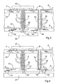
- Figure 1 is a cross section of an optical module including a semiconductor device comprising a semiconductor substrate 1, which may be silicon, for instance.
- a dielectric layer 2 is arranged on or above a main surface 12 of the substrate 1, and a further dielectric layer 3 is arranged on or above the opposite main surface 13 of the substrate 1.
- An optical via 4 penetrates the substrate 1 and provides a light path 11 between the levels of the main surface 12 and the further main surface 13.
- the light path 11 is indicated in Figure 1 by broken lines.
- the optical via 4 is laterally surrounded by a metal via layer 5, which may be gold or copper, for instance, and is preferably insulated form the semiconductor material of the substrate 1 by a dielectric sidewall layer 6.
- the metal via layer 5 is open at both ends and thus forms a metal tube around the light path 11.
- the optical via 4 comprises a void extending through the dielectric layer 2 but not through the further dielectric layer 3, which confines the metal via layer 5 near the level of the further main surface 13 of the substrate 1.
- An optional dielectric cover layer 22 may be applied on the metal via layer 5 in the optical via 4.
- a metal wiring 7 is embedded in the dielectric layer 2, and a further metal wiring 8 is embedded in the further dielectric layer 3.
- the wirings 7, 8 may comprise one or more structured metallization layers and vertical interconnections and may serve as electrical connections of terminals of electronic components integrated in the substrate 1.
- a top metal layer 9 forms a contact for an external electrical connection of a through-substrate via 14, which is provided as an electrical interconnection through the substrate 1.
- the through-substrate via 14 comprises a further metal via layer 15, which is preferably insulated form the semiconductor material of the substrate 1 by a further dielectric sidewall layer 16.
- the further metal via layer 15 is electrically connected with a contact pad 19, which is arranged on the further dielectric layer 3 or embedded in the further dielectric layer 3.
- the contact pad 19 can be part of the further wiring 8 and can thus especially be connected with terminals of integrated components and/or with further contact pads for external electrical connection.
- Bump contacts 17 on the metal wiring 7 serve as electrical connections to an optical device 10 mounted above the main surface 12.
- the optical device 10 may be a vertical cavity surface emitting laser, a photodiode or a wave guide component, for instance.
- Further bump contacts 18 on the further metal wiring 8 serve as electrical connections to a further optical device 20 mounted above the further main surface 13.
- the further optical device 20 may also be a vertical cavity surface emitting laser, a photodiode or a wave guide component, for instance. If the optical device 10 is a light emitting device like a VCSEL, for instance, the further optical device 20 may be a photodiode, for instance.
- the light is emitted in the direction of the light path 11 through the optical via 4 and may be focused into the light receiving area of the photodiode by a lens 23 arranged on the surface of the further dielectric layer 3.
- a lens 23 can be formed by imprinting techniques, especially by nano-imprinting techniques known per se, or it can be mounted as a separate device during assembly of the optical module.
- the embodiment according to Figure 1 is only an example of a variety of applications for an arrangement of optical devices that are optically connected with one another through the optical via 4. Further active optical devices and passive optical devices like mirrors, for instance, may be mounted to the substrate 1. The direction of light propagation may be reversed with respect to the example shown in Figure 1 .
- a plurality of optical vias may be provided in the same substrate for light propagation in different directions, thus connecting a plurality of active and passive optical devices and providing an easy way of optically connecting components arranged in an optoelectronic module.
- the boundary between the dielectric sidewall layer 6 and the metal via layer 5 or the boundary between the metal via layer 5 and the dielectric cover layer 22 may be used for the propagation of light through the optical via 4 by means of surface plasmon-polaritons (SPPs).
- SPPs are collective charge oscillations generated at the interface of a dielectric and a metal by incident photons coupling with surface plasmons. SPPs sustain the propagation of electromagnetic waves along the interface between the dielectric and the metal.
- a metal via layer 5 of gold or copper may be preferred in this embodiment for the generation of SPPs.
- optical via 4 and the through-substrate via 14 have similar structures except for the optical via 4 being open at both ends, whereas the through-substrate via 14 is closed by the contact pad 19. Because of the structural similarities, one or more optical vias 4 and one or more through-substrate vias 14 can be produced together with essentially the same method steps.
- via holes are etched through the substrate 1 from the main surface 12. At least one via hole is provided for an optical via 4 and is formed at a distance from the contact pad 19. At least one further via hole is provided for a through-substrate via 14 serving as electrical interconnection and is formed reaching the contact pad 19. Dielectric sidewall layers 6, 16 are preferably formed at the sidewalls of the via holes to insulate the semiconductor material from metallizations that are subsequently applied.
- the metal via layer 5 is deposited in the shape of a hollow cylinder in the via hole provided for the optical via 4, and the further metal via layer 15 is deposited in the via hole provided for the through-substrate via 14 and may also form a hollow cylinder.
- the further metal via layer 15 contacts the contact pad 19 at the bottom of the via hole.
- the metal via layer 5 is removed from the bottom of the via hole that is provided for the optical via 4, so that the metal via layer 5 is open at both ends and forms a metal tube allowing free passage of light.
- the removal of the bottom portion of the metal via layer 5 can be effected by anisotropically etching, especially by an anisotropic reactive ion etch step (RIE), with no or extremely low etch rate at the vertical sidewall and maximal etch rate on the horizontal bottom surface.
- RIE anisotropic reactive ion etch step
- FIG. 2 is a cross section according to Figure 1 for a further embodiment.
- the embodiment according to Figure 2 comprises a board 21, which may be a printed circuit board comprising conductor tracks and/or wave guides 29, for instance.
- Wave guides 29 arranged in the board 21 are schematically indicated in Figure 2 .
- the light that is guided through the optical via 4 along the light path 11 indicated with broken lines is coupled into the wave guides 29 and propagates through the wave guides 29 in the board 21.
- the further bump contacts 18 are arranged on the further metal wiring 8 and serve as electrical connections to conductor tracks of the board 21.
- Figure 3 is a cross section according to Figure 1 for a further embodiment.
- Components of the embodiment according to Figure 3 that correspond to components of the embodiment according to Figure 1 are designated with the same reference numerals.
- the light path 11 does not lead through a portion of the further dielectric layer 3.
- the central void of the optical via 4 extends through the further dielectric layer 3, so that the light does not have to propagate through a layer of dielectric material.
- the further dielectric layer 3 can be opened at the lower end of the optical via 4 by drilling, for example, or by a masked etching step.
- the arrangement of optical devices 10, 20 mounted to the substrate 1 is represented as in Figure 1 , but this is only one example.
- the substrate 1 of the embodiment according to Figure 3 may instead be mounted on a board 21, for instance, as in the embodiment according to Figure 2 .
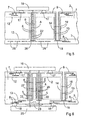
- FIG. 4 is a cross section according to Figure 2 for a further embodiment. Components of the embodiment according to Figure 4 that correspond to components of the embodiment according to Figure 2 are designated with the same reference numerals.
- the light is focused by means of a diffracting element like a zone plate 24 embedded in the further dielectric layer 3.
- a zone plate comprises a set of radially symmetric Fresnel zones, which are spaced to generate constructive interference at the desired focus.
- the Fresnel zones are formed by concentric circular regions of suitably varying diameters, widths and distances, which are formed from a material that has a refractive index different from the refractive index of the further dielectric layer 3.
- a phase shift zone plate wherein half wavelength phase delays are created between adjacent ring zones, or a Fresnel lens can be formed.
- Zone plates, Fresnel lenses and their application to semiconductor devices are known per se and need not be described in detail.
- the arrangement of the substrate 1 with an optical device 10 and a board 21 shown in Figure 4 is similar to the embodiment according to Figure 2 , but other arrangements of optical devices are also suitable in combination with a substrate 1 comprising a zone plate 24, like the devices 10, 20 of the embodiments according to Figure 1 and Figure 3 , for example.
- Figure 5 is a cross section according to Figures 1 to 4 for a further embodiment.
- Components of the embodiment according to Figure 5 that correspond to components of the embodiments according to Figures 1 to 4 are designated with the same reference numerals.
- the light path 11 through the optical via 4 enters a grating coupler 25, which directs the light into a wave guide 26 embedded in the further dielectric layer 3 or arranged on the further dielectric layer 3.
- the wave guide 26 can thus be integrated on the substrate 1, so that an application of a board 21 comprising an external wave guide 29, as in the embodiment according to Figure 2 , may be avoided.
- Figure 6 is a cross section according to Figure 1 for a further embodiment. Components of the embodiment according to Figure 6 that correspond to components of the embodiment according to Figure 1 are designated with the same reference numerals.
- the optical via 4 has the shape of a hollow cylinder surrounding a pillar 27 of the semiconductor material of the substrate 1.
- the metal via layer 5 has the shape of two concentric hollow cylinders, an outer cylinder corresponding to the metal via layer 5 of the embodiments previously described and an inner cylinder forming a central portion of the metal via layer 5 at the sidewall of the pillar 27.
- the optical via 4 extends between the outer cylinder and the inner cylinder of the metal via layer 5.
- the central portion of the metal via layer 5 is preferably insulated from the sidewall of the pillar 27 by a central portion of the dielectric sidewall layer 6.
- a further dielectric cover layer 28 may be arranged on the central portion of the metal via layer 5.
- the boundary between the central portion of the metal via layer 5 and the central portion of the dielectric sidewall layer 6 or the boundary between the central portion of the metal via layer 5 and the further dielectric cover layer 28 may additionally be used for light propagation by means of surface plasmon-polaritons as described above.
- the pillar 27 is formed by etching the via hole for the optical via 4 in the shape of a hollow cylinder.
- the pillar 27 rests on a portion of the further dielectric layer 3.
- the invention has the advantage that light signal transfer is enabled by through-substrate vias that are conventionally created for electrical connections between conductors on one side of a substrate and conductors on the opposite side.
- the necessary modifications of the through-substrate vias do not require a dedicated further etching step and do not go beyond conventional production techniques.
Landscapes
- Physics & Mathematics (AREA)
- General Physics & Mathematics (AREA)
- Optics & Photonics (AREA)
- Engineering & Computer Science (AREA)
- Microelectronics & Electronic Packaging (AREA)
- Optical Integrated Circuits (AREA)
- Optical Couplings Of Light Guides (AREA)
Abstract
Description
- Photodiodes and vertical cavity surface emitting lasers (VCSELs) can be mounted on a semiconductor chip comprising an integrated circuit (IC) to form an optical module, which combines optical functions like optical data transfer, switching, multiplexing and modulation with electronical functions like data processing. A wave guide leading through the semiconductor chip is required for a transfer of optical signals between opposite surfaces of the chip.
-
US 8,231,284 B2 discloses an optical module comprising an array of photodiodes and VCSELS mounted to a single-chip CMOS optical transceiver in flip-chip technology. -
US 8,265,432 B2 discloses an optical module comprising a chip with integrated circuit, optical windows and a plurality of optoelectronic devices, which are positioned in alignment with the windows and attached in flip-chip technology. -
US 8,488,921 B2 discloses an arrangement of an electronic IC with optical vias providing access for multicore fibers to a plurality of photodiodes and VCSELs. -
US 2013/0099256 A1 discloses a multi-chip package of chips each having a light receiving element in the sidewall of a via hole. The chips are stacked on a substrate with the via holes aligned. An optical signal from a light emitting element of the substrate is focused by an electrically adjustable lens into the light receiving elements. - It is an object of the present invention to disclose a device that facilitates the optical connection between components of an optical module. It is a further object of the invention to disclose a method of producing such a device.
- This object is achieved with the semiconductor device with optical via according to claim 1, with the optical module according to
claim 10, and with the method of producing a semiconductor device with optical via according toclaim 15. Embodiments and variants derive from the dependent claims. - The semiconductor device comprises a semiconductor substrate having a main surface and a further main surface opposite the main surface and an optical via penetrating the substrate from the main surface to the further main surface. A metal via layer is arranged along the optical via without closing the optical via. Contrary to a conventional through-substrate via, the metal via layer of the optical via is not provided with a metal landing pad barring one end of the via, so that the optical path is not interrupted by a metal pad.
- In an embodiment of the semiconductor device, a contact pad is arranged above the further main surface at a distance from the optical via. A through-substrate via comprising a further metal via layer is arranged in the substrate, the through-substrate via penetrating the substrate from the main surface to the contact pad. The further metal via layer is in electrical contact with the contact pad.
- In a further embodiment of the semiconductor device, a dielectric layer is present on the main surface, and the optical via extends through the dielectric layer. A top metal layer is arranged in or on the dielectric layer. A further dielectric layer is present on the further main surface. The contact pad is embedded in the further dielectric layer. The further metal via layer electrically connects the top metal layer with the contact pad.
- In a further embodiment, a zone plate is arranged in the further dielectric layer above the optical via.
- In a further embodiment, a grating coupler is arranged in the further dielectric layer above the optical via, and a wave guide is arranged in the further dielectric layer level with the grating coupler.
- In a further embodiment, a dielectric cover layer is arranged on the metal via layer along the optical via.
- In a further embodiment, the metal via layer is gold or copper.
- In a further embodiment, the optical via is in the shape of a hollow cylinder surrounding a pillar of the semiconductor substrate.
- In a further embodiment, a further dielectric cover layer is arranged on the pillar along the optical via.
- An optical module comprising the semiconductor device further comprises an optical device arranged above the main surface and above the optical via.
- An embodiment of the optical module comprises a further optical device arranged above the further main surface and above the optical via.
- In a further embodiment of the optical module, the optical device is a vertical cavity surface emitting laser (VCSEL), a photodiode or a wave guide component, and the further optical device is a vertical cavity surface emitting laser, a photodiode or a wave guide component.
- A further embodiment of the optical module comprises a metal wiring above the main surface, a further metal wiring above the further main surface, bump contacts connecting the optical device to the metal wiring, and further bump contacts connecting the further optical device to the further metal wiring.
- A further embodiment of the optical module comprises a board with a wave guide. The semiconductor device is mounted on the board, so that the optical via is arranged in correspondence with the wave guide of the board.
- The method of producing a semiconductor device with optical via comprises the steps of providing a semiconductor substrate having a main surface and an opposite further main surface with a contact pad arranged above the further main surface, forming a through-substrate via from the main surface to the further main surface at a distance from the contact pad and a further through-substrate via from the main surface to the further main surface above the contact pad, arranging a hollow metal via layer in the through-substrate via and a further metal via layer in the further through-substrate via, so that the further metal via layer contacts the contact pad, and removing a bottom portion of the metal via layer to form an optical via laterally surrounded by the metal via layer.
- In a variant of the method, a dielectric cover layer is arranged on the metal via layer, the dielectric cover layer laterally surrounding the optical via.
- In a further variant of the method, the through-substrate via provided for the optical via is formed in the shape of a hollow cylinder surrounding a pillar of the substrate.
- The following is a detailed description of examples of the semiconductor device, the optical module and the method of producing the semiconductor device in conjunction with the appended figures.
- Figure 1
- is a cross section of an embodiment of an optical module including the semiconductor device.
- Figure 2
- is a cross section of a further embodiment mounted on a board.
- Figure 3
- is a cross section of a further embodiment comprising a prolonged cavity of the optical via.
- Figure 4
- is a cross section of a further embodiment comprising a zone plate.
- Figure 5
- is a cross section of a further embodiment comprising a grating coupler.
- Figure 6
- is a cross section of a further embodiment with a central pillar of semiconductor material arranged in the optical via.
-
Figure 1 is a cross section of an optical module including a semiconductor device comprising a semiconductor substrate 1, which may be silicon, for instance. Adielectric layer 2 is arranged on or above amain surface 12 of the substrate 1, and a furtherdielectric layer 3 is arranged on or above the oppositemain surface 13 of the substrate 1. Anoptical via 4 penetrates the substrate 1 and provides alight path 11 between the levels of themain surface 12 and the furthermain surface 13. Thelight path 11 is indicated inFigure 1 by broken lines. Theoptical via 4 is laterally surrounded by a metal vialayer 5, which may be gold or copper, for instance, and is preferably insulated form the semiconductor material of the substrate 1 by adielectric sidewall layer 6. The metal vialayer 5 is open at both ends and thus forms a metal tube around thelight path 11. In the example shown inFigure 1 , theoptical via 4 comprises a void extending through thedielectric layer 2 but not through the furtherdielectric layer 3, which confines the metal vialayer 5 near the level of the furthermain surface 13 of the substrate 1. An optionaldielectric cover layer 22 may be applied on the metal vialayer 5 in the optical via 4. - A
metal wiring 7 is embedded in thedielectric layer 2, and afurther metal wiring 8 is embedded in the furtherdielectric layer 3. Thewirings top metal layer 9 forms a contact for an external electrical connection of a through-substrate via 14, which is provided as an electrical interconnection through the substrate 1. The through-substrate via 14 comprises a further metal vialayer 15, which is preferably insulated form the semiconductor material of the substrate 1 by a furtherdielectric sidewall layer 16. The further metal vialayer 15 is electrically connected with acontact pad 19, which is arranged on the furtherdielectric layer 3 or embedded in the furtherdielectric layer 3. Thecontact pad 19 can be part of thefurther wiring 8 and can thus especially be connected with terminals of integrated components and/or with further contact pads for external electrical connection. -
Bump contacts 17 on themetal wiring 7 serve as electrical connections to anoptical device 10 mounted above themain surface 12. Theoptical device 10 may be a vertical cavity surface emitting laser, a photodiode or a wave guide component, for instance.Further bump contacts 18 on thefurther metal wiring 8 serve as electrical connections to a furtheroptical device 20 mounted above the furthermain surface 13. The furtheroptical device 20 may also be a vertical cavity surface emitting laser, a photodiode or a wave guide component, for instance. If theoptical device 10 is a light emitting device like a VCSEL, for instance, the furtheroptical device 20 may be a photodiode, for instance. The light is emitted in the direction of thelight path 11 through the optical via 4 and may be focused into the light receiving area of the photodiode by alens 23 arranged on the surface of thefurther dielectric layer 3. Such alens 23 can be formed by imprinting techniques, especially by nano-imprinting techniques known per se, or it can be mounted as a separate device during assembly of the optical module. - The embodiment according to
Figure 1 is only an example of a variety of applications for an arrangement of optical devices that are optically connected with one another through the optical via 4. Further active optical devices and passive optical devices like mirrors, for instance, may be mounted to the substrate 1. The direction of light propagation may be reversed with respect to the example shown inFigure 1 . A plurality of optical vias may be provided in the same substrate for light propagation in different directions, thus connecting a plurality of active and passive optical devices and providing an easy way of optically connecting components arranged in an optoelectronic module. - The boundary between the
dielectric sidewall layer 6 and the metal vialayer 5 or the boundary between the metal vialayer 5 and thedielectric cover layer 22 may be used for the propagation of light through the optical via 4 by means of surface plasmon-polaritons (SPPs). SPPs are collective charge oscillations generated at the interface of a dielectric and a metal by incident photons coupling with surface plasmons. SPPs sustain the propagation of electromagnetic waves along the interface between the dielectric and the metal. A metal vialayer 5 of gold or copper may be preferred in this embodiment for the generation of SPPs. - The optical via 4 and the through-substrate via 14 have similar structures except for the optical via 4 being open at both ends, whereas the through-substrate via 14 is closed by the
contact pad 19. Because of the structural similarities, one or moreoptical vias 4 and one or more through-substrate vias 14 can be produced together with essentially the same method steps. - In the method of production, via holes are etched through the substrate 1 from the
main surface 12. At least one via hole is provided for an optical via 4 and is formed at a distance from thecontact pad 19. At least one further via hole is provided for a through-substrate via 14 serving as electrical interconnection and is formed reaching thecontact pad 19. Dielectric sidewall layers 6, 16 are preferably formed at the sidewalls of the via holes to insulate the semiconductor material from metallizations that are subsequently applied. The metal vialayer 5 is deposited in the shape of a hollow cylinder in the via hole provided for the optical via 4, and the further metal vialayer 15 is deposited in the via hole provided for the through-substrate via 14 and may also form a hollow cylinder. The further metal vialayer 15 contacts thecontact pad 19 at the bottom of the via hole. The metal vialayer 5 is removed from the bottom of the via hole that is provided for the optical via 4, so that the metal vialayer 5 is open at both ends and forms a metal tube allowing free passage of light. The removal of the bottom portion of the metal vialayer 5 can be effected by anisotropically etching, especially by an anisotropic reactive ion etch step (RIE), with no or extremely low etch rate at the vertical sidewall and maximal etch rate on the horizontal bottom surface. -
Figure 2 is a cross section according toFigure 1 for a further embodiment. Components of the embodiment according toFigure 2 that correspond to components of the embodiment according toFigure 1 are designated with the same reference numerals. The embodiment according toFigure 2 comprises aboard 21, which may be a printed circuit board comprising conductor tracks and/or wave guides 29, for instance. Wave guides 29 arranged in theboard 21 are schematically indicated inFigure 2 . The light that is guided through the optical via 4 along thelight path 11 indicated with broken lines is coupled into the wave guides 29 and propagates through the wave guides 29 in theboard 21. In the embodiment according toFigure 2 , thefurther bump contacts 18 are arranged on thefurther metal wiring 8 and serve as electrical connections to conductor tracks of theboard 21. -
Figure 3 is a cross section according toFigure 1 for a further embodiment. Components of the embodiment according toFigure 3 that correspond to components of the embodiment according toFigure 1 are designated with the same reference numerals. In the embodiment according toFigure 3 , thelight path 11 does not lead through a portion of thefurther dielectric layer 3. Instead, the central void of the optical via 4 extends through thefurther dielectric layer 3, so that the light does not have to propagate through a layer of dielectric material. In the manufacturing process, thefurther dielectric layer 3 can be opened at the lower end of the optical via 4 by drilling, for example, or by a masked etching step. InFigure 3 , the arrangement ofoptical devices Figure 1 , but this is only one example. The substrate 1 of the embodiment according toFigure 3 may instead be mounted on aboard 21, for instance, as in the embodiment according toFigure 2 . -
Figure 4 is a cross section according toFigure 2 for a further embodiment. Components of the embodiment according toFigure 4 that correspond to components of the embodiment according toFigure 2 are designated with the same reference numerals. In the embodiment according toFigure 4 , the light is focused by means of a diffracting element like azone plate 24 embedded in thefurther dielectric layer 3. A zone plate comprises a set of radially symmetric Fresnel zones, which are spaced to generate constructive interference at the desired focus. The Fresnel zones are formed by concentric circular regions of suitably varying diameters, widths and distances, which are formed from a material that has a refractive index different from the refractive index of thefurther dielectric layer 3. By suitably adapting the shape of the concentric circular regions, a phase shift zone plate, wherein half wavelength phase delays are created between adjacent ring zones, or a Fresnel lens can be formed. Zone plates, Fresnel lenses and their application to semiconductor devices are known per se and need not be described in detail. The arrangement of the substrate 1 with anoptical device 10 and aboard 21 shown inFigure 4 is similar to the embodiment according toFigure 2 , but other arrangements of optical devices are also suitable in combination with a substrate 1 comprising azone plate 24, like thedevices Figure 1 andFigure 3 , for example. -
Figure 5 is a cross section according toFigures 1 to 4 for a further embodiment. Components of the embodiment according toFigure 5 that correspond to components of the embodiments according toFigures 1 to 4 are designated with the same reference numerals. In the embodiment according toFigure 5 , thelight path 11 through the optical via 4 enters agrating coupler 25, which directs the light into awave guide 26 embedded in thefurther dielectric layer 3 or arranged on thefurther dielectric layer 3. Thewave guide 26 can thus be integrated on the substrate 1, so that an application of aboard 21 comprising anexternal wave guide 29, as in the embodiment according toFigure 2 , may be avoided. -
Figure 6 is a cross section according toFigure 1 for a further embodiment. Components of the embodiment according toFigure 6 that correspond to components of the embodiment according toFigure 1 are designated with the same reference numerals. In the embodiment according toFigure 6 , the optical via 4 has the shape of a hollow cylinder surrounding apillar 27 of the semiconductor material of the substrate 1. The metal vialayer 5 has the shape of two concentric hollow cylinders, an outer cylinder corresponding to the metal vialayer 5 of the embodiments previously described and an inner cylinder forming a central portion of the metal vialayer 5 at the sidewall of thepillar 27. The optical via 4 extends between the outer cylinder and the inner cylinder of the metal vialayer 5. The central portion of the metal vialayer 5 is preferably insulated from the sidewall of thepillar 27 by a central portion of thedielectric sidewall layer 6. - A further
dielectric cover layer 28 may be arranged on the central portion of the metal vialayer 5. The boundary between the central portion of the metal vialayer 5 and the central portion of thedielectric sidewall layer 6 or the boundary between the central portion of the metal vialayer 5 and the furtherdielectric cover layer 28 may additionally be used for light propagation by means of surface plasmon-polaritons as described above. - The
pillar 27 is formed by etching the via hole for the optical via 4 in the shape of a hollow cylinder. Thepillar 27 rests on a portion of thefurther dielectric layer 3. - The invention has the advantage that light signal transfer is enabled by through-substrate vias that are conventionally created for electrical connections between conductors on one side of a substrate and conductors on the opposite side. The necessary modifications of the through-substrate vias do not require a dedicated further etching step and do not go beyond conventional production techniques.
-
- 1
- substrate
- 2
- dielectric layer
- 3
- further dielectric layer
- 4
- optical via
- 5
- metal via layer
- 6
- dielectric sidewall layer
- 7
- metal wiring
- 8
- further metal wiring
- 9
- top metal layer
- 10
- optical device
- 11
- light path
- 12
- main surface
- 13
- further main surface
- 14
- through-substrate via
- 15
- further metal via layer
- 16
- further dielectric sidewall layer
- 17
- bump contact
- 18
- further bump contact
- 19
- contact pad
- 20
- further optical device
- 21
- board
- 22
- dielectric cover layer
- 23
- lens
- 24
- zone plate
- 25
- grating coupler
- 26
- wave guide
- 27
- pillar
- 28
- further dielectric cover layer
- 29
- wave guide
Claims (17)
- A semiconductor device with optical via, comprising:- a semiconductor substrate (1) having a main surface (12) and a further main surface (13) opposite the main surface (12), and- an optical via (4) penetrating the substrate (1) from the main surface (12) to the further main surface (13),
characterized in that- a metal via layer (5) is arranged along the optical via (4) without closing the optical via (4). - The semiconductor device of claim 1, further comprising:- a contact pad (19) arranged above the further main surface (13) at a distance from the optical via (4),- a through-substrate via (14) comprising a further metal via layer (15) arranged in the substrate (1), the through-substrate via (14) penetrating the substrate (1) from the main surface (12) to the contact pad (19), and- the further metal via layer (15) being in electrical contact with the contact pad (19).
- The semiconductor device of claim 2, further comprising:- a dielectric layer (2) on the main surface (12), the optical via (4) extending through the dielectric layer (2),- a top metal layer (9) arranged in or on the dielectric layer (2),- a further dielectric layer (3) on the further main surface (13),- the contact pad (19) being embedded in the further dielectric layer (3), and- the further metal via layer (15) electrically connecting the top metal layer (9) with the contact pad (19).
- The semiconductor device of claim 3, further comprising:a zone plate (24) arranged in the further dielectric layer (3) above the optical via (4).
- The semiconductor device of claim 3, further comprising:a grating coupler (25) arranged in the further dielectric layer (3) above the optical via (4), anda wave guide (26) arranged in the further dielectric layer (3) level with the grating coupler (25).
- The semiconductor device of one of claims 1 to 5, further comprising:a dielectric cover layer (22) arranged on the metal via layer (5) along the optical via (4).
- The semiconductor device of one of claims 1 to 6, wherein the metal via layer (5) is copper or gold.
- The semiconductor device of one of claims 1 to 7, wherein the optical via (4) is in the shape of a hollow cylinder surrounding a pillar (27) of the semiconductor substrate (1).
- The semiconductor device of claim 8, further comprising:a further dielectric cover layer (28) arranged on the pillar (27) along the optical via (4).
- An optical module comprising the semiconductor device of one of claims 1 to 9, further comprising:an optical device (10) arranged above the main surface (12) and above the optical via (4).
- The optical module of claim 10, further comprising:a further optical device (20) arranged above the further main surface (13) and above the optical via (4).
- The optical module of claim 10 or 11, wherein:each of the optical device (10) and the further optical device (20) is a device selected from the group consisting of a vertical cavity surface emitting laser, a photodiode and a wave guide component.
- The optical module of claim 11 or 12, further comprising:a metal wiring (7) above the main surface (12),a further metal wiring (8) above the further main surface (13),bump contacts (17) connecting the optical device (10) to the metal wiring (7), andfurther bump contacts (18) connecting the further optical device (20) to the further metal wiring (8).
- The optical module of one of claims 10 to 13, further comprising:a board (21) comprising a wave guide (29), the semiconductor device being mounted on the board (21) with the optical via (4) arranged in correspondence with the wave guide (29).
- A method of producing a semiconductor device with optical via, comprising:- providing a semiconductor substrate (1) having a main surface (12) and an opposite further main surface (13) with a contact pad (19) arranged above the further main surface (13),- forming a through-substrate via (4) from the main surface (12) to the further main surface (13) at a distance from the contact pad (19) and a further through-substrate via (14) from the main surface (12) to the further main surface (13) above the contact pad (19),- arranging a hollow metal via layer (5) in the through-substrate via (4) and a further metal via layer (15) in the further through-substrate via (14), the further metal via layer (15) contacting the contact pad (19), and- removing a bottom portion of the metal via layer (5) to form an optical via (4) laterally surrounded by the metal via layer (5).
- The method of claim 15, further comprising:arranging a dielectric cover layer (22) on the metal via layer (5), the dielectric cover layer (22) laterally surrounding the optical via (4).
- The method of claim 15 or 16, wherein:the through-substrate via provided for the optical via (4) is formed in the shape of a hollow cylinder surrounding a pillar (27) of the substrate (1).
Priority Applications (3)
| Application Number | Priority Date | Filing Date | Title |
|---|---|---|---|
| EP13188483.5A EP2860560B1 (en) | 2013-10-14 | 2013-10-14 | Semiconductor device with optical and electrical vias |
| PCT/EP2014/071560 WO2015055480A1 (en) | 2013-10-14 | 2014-10-08 | Semiconductor device with optical and electrical vias |
| US15/028,934 US9995894B2 (en) | 2013-10-14 | 2014-10-08 | Semiconductor device with optical and electrical vias |
Applications Claiming Priority (1)
| Application Number | Priority Date | Filing Date | Title |
|---|---|---|---|
| EP13188483.5A EP2860560B1 (en) | 2013-10-14 | 2013-10-14 | Semiconductor device with optical and electrical vias |
Publications (2)
| Publication Number | Publication Date |
|---|---|
| EP2860560A1 true EP2860560A1 (en) | 2015-04-15 |
| EP2860560B1 EP2860560B1 (en) | 2019-07-24 |
Family
ID=49328434
Family Applications (1)
| Application Number | Title | Priority Date | Filing Date |
|---|---|---|---|
| EP13188483.5A Active EP2860560B1 (en) | 2013-10-14 | 2013-10-14 | Semiconductor device with optical and electrical vias |
Country Status (3)
| Country | Link |
|---|---|
| US (1) | US9995894B2 (en) |
| EP (1) | EP2860560B1 (en) |
| WO (1) | WO2015055480A1 (en) |
Cited By (2)
| Publication number | Priority date | Publication date | Assignee | Title |
|---|---|---|---|---|
| US20150063745A1 (en) * | 2013-08-29 | 2015-03-05 | Industrial Technology Research Institute | Optical coupling module |
| US12100644B2 (en) | 2018-12-21 | 2024-09-24 | Ams Ag | Semiconductor device with through-substrate via and method of manufacturing a semiconductor device with through-substrate via |
Families Citing this family (7)
| Publication number | Priority date | Publication date | Assignee | Title |
|---|---|---|---|---|
| US10585254B2 (en) | 2017-11-17 | 2020-03-10 | Samsung Electronics Co., Ltd. | Vertical optical via and method of fabrication |
| DE102019127915A1 (en) | 2019-10-16 | 2021-04-22 | Tdk Electronics Ag | Sensor element and method for producing a sensor element |
| DE102019127924B3 (en) * | 2019-10-16 | 2021-01-21 | Tdk Electronics Ag | Component and method for manufacturing a component |
| EP3813101B1 (en) | 2019-10-25 | 2026-03-25 | ams AG | Method of producing a semiconductor body with a trench |
| US12489189B2 (en) * | 2021-06-16 | 2025-12-02 | Intel Corporation | Contactless communication using a waveguide extending through a substrate core |
| US11796735B2 (en) * | 2021-07-06 | 2023-10-24 | Taiwan Semiconductor Manufacturing Co., Ltd. | Integrated 3DIC with stacked photonic dies and method forming same |
| DE102024128738A1 (en) | 2024-10-04 | 2026-04-09 | Technische Universität Dresden, Körperschaft des öffentlichen Rechts | Semiconductor arrays and semiconductor packages |
Citations (11)
| Publication number | Priority date | Publication date | Assignee | Title |
|---|---|---|---|---|
| EP0017701A1 (en) * | 1979-04-16 | 1980-10-29 | International Business Machines Corporation | Coupling device for a substrate-mounted optical transducer |
| EP0175936A1 (en) * | 1984-09-24 | 1986-04-02 | Siemens Aktiengesellschaft | Opto-electronic device |
| WO2003039216A1 (en) * | 2001-11-02 | 2003-05-08 | Imego Ab | Carrier arrangement for carrying optical components and connecting optical signals and method of manufacturing the same |
| US20070085215A1 (en) * | 2003-09-30 | 2007-04-19 | Budd Russell A | Silicon based optical vias |
| US20100195954A1 (en) * | 2004-10-22 | 2010-08-05 | Ibiden Co., Ltd. | Multilayer printed circuit board |
| US8231284B2 (en) | 2007-03-26 | 2012-07-31 | International Business Machines Corporation | Ultra-high bandwidth, multiple-channel full-duplex, single-chip CMOS optical transceiver |
| US8265432B2 (en) | 2008-03-10 | 2012-09-11 | International Business Machines Corporation | Optical transceiver module with optical windows |
| EP1491927B1 (en) * | 2002-04-01 | 2013-02-27 | Ibiden Co., Ltd. | Ic chip mounting substrate, and ic chip mounting substrate manufacturing method |
| US20130099256A1 (en) | 2011-10-21 | 2013-04-25 | SK Hynix Inc. | Multi-chip package cross-reference to related applications |
| US20130177277A1 (en) * | 2010-10-01 | 2013-07-11 | Sumitomo Bakelite Co. Ltd. | Optical waveguide, method for producing optical waveguide, optical waveguide module, method for producing optical waveguide module, and electronic apparatus |
| US8488921B2 (en) | 2010-07-16 | 2013-07-16 | International Business Machines Corporation | Packaged multicore fiber optical transceiver module |
Family Cites Families (2)
| Publication number | Priority date | Publication date | Assignee | Title |
|---|---|---|---|---|
| DE102011104305A1 (en) * | 2011-06-16 | 2012-12-20 | Austriamicrosystems Ag | Production method for a semiconductor component with a conductor layer in the semiconductor body and semiconductor component |
| EP2620978B1 (en) * | 2012-01-25 | 2019-07-24 | austriamicrosystems AG | Semiconductor device with internal substrate contact and method of production |
-
2013
- 2013-10-14 EP EP13188483.5A patent/EP2860560B1/en active Active
-
2014
- 2014-10-08 US US15/028,934 patent/US9995894B2/en active Active
- 2014-10-08 WO PCT/EP2014/071560 patent/WO2015055480A1/en not_active Ceased
Patent Citations (11)
| Publication number | Priority date | Publication date | Assignee | Title |
|---|---|---|---|---|
| EP0017701A1 (en) * | 1979-04-16 | 1980-10-29 | International Business Machines Corporation | Coupling device for a substrate-mounted optical transducer |
| EP0175936A1 (en) * | 1984-09-24 | 1986-04-02 | Siemens Aktiengesellschaft | Opto-electronic device |
| WO2003039216A1 (en) * | 2001-11-02 | 2003-05-08 | Imego Ab | Carrier arrangement for carrying optical components and connecting optical signals and method of manufacturing the same |
| EP1491927B1 (en) * | 2002-04-01 | 2013-02-27 | Ibiden Co., Ltd. | Ic chip mounting substrate, and ic chip mounting substrate manufacturing method |
| US20070085215A1 (en) * | 2003-09-30 | 2007-04-19 | Budd Russell A | Silicon based optical vias |
| US20100195954A1 (en) * | 2004-10-22 | 2010-08-05 | Ibiden Co., Ltd. | Multilayer printed circuit board |
| US8231284B2 (en) | 2007-03-26 | 2012-07-31 | International Business Machines Corporation | Ultra-high bandwidth, multiple-channel full-duplex, single-chip CMOS optical transceiver |
| US8265432B2 (en) | 2008-03-10 | 2012-09-11 | International Business Machines Corporation | Optical transceiver module with optical windows |
| US8488921B2 (en) | 2010-07-16 | 2013-07-16 | International Business Machines Corporation | Packaged multicore fiber optical transceiver module |
| US20130177277A1 (en) * | 2010-10-01 | 2013-07-11 | Sumitomo Bakelite Co. Ltd. | Optical waveguide, method for producing optical waveguide, optical waveguide module, method for producing optical waveguide module, and electronic apparatus |
| US20130099256A1 (en) | 2011-10-21 | 2013-04-25 | SK Hynix Inc. | Multi-chip package cross-reference to related applications |
Cited By (3)
| Publication number | Priority date | Publication date | Assignee | Title |
|---|---|---|---|---|
| US20150063745A1 (en) * | 2013-08-29 | 2015-03-05 | Industrial Technology Research Institute | Optical coupling module |
| US9613886B2 (en) * | 2013-08-29 | 2017-04-04 | Industrial Technology Research Institute | Optical coupling module |
| US12100644B2 (en) | 2018-12-21 | 2024-09-24 | Ams Ag | Semiconductor device with through-substrate via and method of manufacturing a semiconductor device with through-substrate via |
Also Published As
| Publication number | Publication date |
|---|---|
| EP2860560B1 (en) | 2019-07-24 |
| US20160259139A1 (en) | 2016-09-08 |
| WO2015055480A1 (en) | 2015-04-23 |
| US9995894B2 (en) | 2018-06-12 |
Similar Documents
| Publication | Publication Date | Title |
|---|---|---|
| EP2860560B1 (en) | Semiconductor device with optical and electrical vias | |
| KR102797203B1 (en) | Integrated 3dic with stacked photonic dies and method forming same | |
| US11611004B2 (en) | Opto-electronic integrated circuit and computing apparatus | |
| KR101955060B1 (en) | Optical interposer | |
| US7271461B2 (en) | Stackable optoelectronics chip-to-chip interconnects and method of manufacturing | |
| US5652811A (en) | Semiconductor on fiber optic substrate (SOFOS) | |
| US12181722B2 (en) | Structures and process flow for integrated photonic-electric ic package by using polymer waveguide | |
| CN114488414A (en) | Modular assembly for photovoltaic systems | |
| US20120014641A1 (en) | Optical-electrical wiring board and optical module | |
| US20250306301A1 (en) | Manufacturing method of package structure having grating coupler | |
| US12334362B2 (en) | Package structure including photonic package having embedded optical glue | |
| US20260110840A1 (en) | Fabrication method of apparatus for optical coupling | |
| JP4412105B2 (en) | Optical waveguide device | |
| US7622700B2 (en) | Photo-electric conversion apparatus with alternating photoelectric conversion elements | |
| KR20250045571A (en) | Semiconductor package | |
| CN117092764A (en) | A 400G optoelectronic co-packaged module structure | |
| JP2005317658A (en) | Optical / electrical batch connection board | |
| CN220568968U (en) | Package structure | |
| US20250125312A1 (en) | Semiconductor package including photonic chip | |
| KR20250054574A (en) | Semiconductor package | |
| US20260029576A1 (en) | Chip structure and semiconductor package including the same | |
| KR20260043859A (en) | Semiconductor package and method for manufacturing the same | |
| KR20250040365A (en) | Semiconductor package | |
| CN119065075A (en) | Photonic components and methods of forming the same | |
| JP2014225029A (en) | Manufacturing method of optical module |
Legal Events
| Date | Code | Title | Description |
|---|---|---|---|
| PUAI | Public reference made under article 153(3) epc to a published international application that has entered the european phase |
Free format text: ORIGINAL CODE: 0009012 |
|
| 17P | Request for examination filed |
Effective date: 20131014 |
|
| AK | Designated contracting states |
Kind code of ref document: A1 Designated state(s): AL AT BE BG CH CY CZ DE DK EE ES FI FR GB GR HR HU IE IS IT LI LT LU LV MC MK MT NL NO PL PT RO RS SE SI SK SM TR |
|
| AX | Request for extension of the european patent |
Extension state: BA ME |
|
| R17P | Request for examination filed (corrected) |
Effective date: 20150916 |
|
| RBV | Designated contracting states (corrected) |
Designated state(s): AL AT BE BG CH CY CZ DE DK EE ES FI FR GB GR HR HU IE IS IT LI LT LU LV MC MK MT NL NO PL PT RO RS SE SI SK SM TR |
|
| RAP1 | Party data changed (applicant data changed or rights of an application transferred) |
Owner name: AMS AG |
|
| GRAP | Despatch of communication of intention to grant a patent |
Free format text: ORIGINAL CODE: EPIDOSNIGR1 |
|
| STAA | Information on the status of an ep patent application or granted ep patent |
Free format text: STATUS: GRANT OF PATENT IS INTENDED |
|
| RIC1 | Information provided on ipc code assigned before grant |
Ipc: H05K 1/02 20060101ALI20190114BHEP Ipc: G02B 6/13 20060101ALN20190114BHEP Ipc: H01L 23/48 20060101ALI20190114BHEP Ipc: H05K 3/42 20060101ALN20190114BHEP Ipc: H01L 31/16 20060101ALN20190114BHEP Ipc: G02B 6/12 20060101ALN20190114BHEP Ipc: H05K 1/11 20060101ALN20190114BHEP Ipc: G02B 6/42 20060101AFI20190114BHEP Ipc: H05K 1/18 20060101ALN20190114BHEP Ipc: H05K 3/46 20060101ALI20190114BHEP Ipc: H01L 23/522 20060101ALN20190114BHEP Ipc: G02B 6/43 20060101ALI20190114BHEP |
|
| RIC1 | Information provided on ipc code assigned before grant |
Ipc: H05K 3/46 20060101ALI20190129BHEP Ipc: G02B 6/42 20060101AFI20190129BHEP Ipc: G02B 6/12 20060101ALN20190129BHEP Ipc: H01L 23/522 20060101ALN20190129BHEP Ipc: H05K 1/18 20060101ALN20190129BHEP Ipc: H05K 1/11 20060101ALN20190129BHEP Ipc: H05K 3/42 20060101ALN20190129BHEP Ipc: H01L 23/48 20060101ALI20190129BHEP Ipc: G02B 6/13 20060101ALN20190129BHEP Ipc: G02B 6/43 20060101ALI20190129BHEP Ipc: H05K 1/02 20060101ALI20190129BHEP Ipc: H01L 31/16 20060101ALN20190129BHEP |
|
| INTG | Intention to grant announced |
Effective date: 20190212 |
|
| GRAS | Grant fee paid |
Free format text: ORIGINAL CODE: EPIDOSNIGR3 |
|
| GRAA | (expected) grant |
Free format text: ORIGINAL CODE: 0009210 |
|
| STAA | Information on the status of an ep patent application or granted ep patent |
Free format text: STATUS: THE PATENT HAS BEEN GRANTED |
|
| AK | Designated contracting states |
Kind code of ref document: B1 Designated state(s): AL AT BE BG CH CY CZ DE DK EE ES FI FR GB GR HR HU IE IS IT LI LT LU LV MC MK MT NL NO PL PT RO RS SE SI SK SM TR |
|
| REG | Reference to a national code |
Ref country code: GB Ref legal event code: FG4D |
|
| REG | Reference to a national code |
Ref country code: CH Ref legal event code: EP |
|
| REG | Reference to a national code |
Ref country code: DE Ref legal event code: R096 Ref document number: 602013058115 Country of ref document: DE |
|
| REG | Reference to a national code |
Ref country code: AT Ref legal event code: REF Ref document number: 1158863 Country of ref document: AT Kind code of ref document: T Effective date: 20190815 |
|
| REG | Reference to a national code |
Ref country code: IE Ref legal event code: FG4D |
|
| REG | Reference to a national code |
Ref country code: NL Ref legal event code: MP Effective date: 20190724 |
|
| REG | Reference to a national code |
Ref country code: LT Ref legal event code: MG4D |
|
| REG | Reference to a national code |
Ref country code: AT Ref legal event code: MK05 Ref document number: 1158863 Country of ref document: AT Kind code of ref document: T Effective date: 20190724 |
|
| PG25 | Lapsed in a contracting state [announced via postgrant information from national office to epo] |
Ref country code: LT Free format text: LAPSE BECAUSE OF FAILURE TO SUBMIT A TRANSLATION OF THE DESCRIPTION OR TO PAY THE FEE WITHIN THE PRESCRIBED TIME-LIMIT Effective date: 20190724 Ref country code: HR Free format text: LAPSE BECAUSE OF FAILURE TO SUBMIT A TRANSLATION OF THE DESCRIPTION OR TO PAY THE FEE WITHIN THE PRESCRIBED TIME-LIMIT Effective date: 20190724 Ref country code: PT Free format text: LAPSE BECAUSE OF FAILURE TO SUBMIT A TRANSLATION OF THE DESCRIPTION OR TO PAY THE FEE WITHIN THE PRESCRIBED TIME-LIMIT Effective date: 20191125 Ref country code: AT Free format text: LAPSE BECAUSE OF FAILURE TO SUBMIT A TRANSLATION OF THE DESCRIPTION OR TO PAY THE FEE WITHIN THE PRESCRIBED TIME-LIMIT Effective date: 20190724 Ref country code: NO Free format text: LAPSE BECAUSE OF FAILURE TO SUBMIT A TRANSLATION OF THE DESCRIPTION OR TO PAY THE FEE WITHIN THE PRESCRIBED TIME-LIMIT Effective date: 20191024 Ref country code: SE Free format text: LAPSE BECAUSE OF FAILURE TO SUBMIT A TRANSLATION OF THE DESCRIPTION OR TO PAY THE FEE WITHIN THE PRESCRIBED TIME-LIMIT Effective date: 20190724 Ref country code: FI Free format text: LAPSE BECAUSE OF FAILURE TO SUBMIT A TRANSLATION OF THE DESCRIPTION OR TO PAY THE FEE WITHIN THE PRESCRIBED TIME-LIMIT Effective date: 20190724 Ref country code: BG Free format text: LAPSE BECAUSE OF FAILURE TO SUBMIT A TRANSLATION OF THE DESCRIPTION OR TO PAY THE FEE WITHIN THE PRESCRIBED TIME-LIMIT Effective date: 20191024 Ref country code: NL Free format text: LAPSE BECAUSE OF FAILURE TO SUBMIT A TRANSLATION OF THE DESCRIPTION OR TO PAY THE FEE WITHIN THE PRESCRIBED TIME-LIMIT Effective date: 20190724 |
|
| PG25 | Lapsed in a contracting state [announced via postgrant information from national office to epo] |
Ref country code: RS Free format text: LAPSE BECAUSE OF FAILURE TO SUBMIT A TRANSLATION OF THE DESCRIPTION OR TO PAY THE FEE WITHIN THE PRESCRIBED TIME-LIMIT Effective date: 20190724 Ref country code: IS Free format text: LAPSE BECAUSE OF FAILURE TO SUBMIT A TRANSLATION OF THE DESCRIPTION OR TO PAY THE FEE WITHIN THE PRESCRIBED TIME-LIMIT Effective date: 20191124 Ref country code: GR Free format text: LAPSE BECAUSE OF FAILURE TO SUBMIT A TRANSLATION OF THE DESCRIPTION OR TO PAY THE FEE WITHIN THE PRESCRIBED TIME-LIMIT Effective date: 20191025 Ref country code: AL Free format text: LAPSE BECAUSE OF FAILURE TO SUBMIT A TRANSLATION OF THE DESCRIPTION OR TO PAY THE FEE WITHIN THE PRESCRIBED TIME-LIMIT Effective date: 20190724 Ref country code: LV Free format text: LAPSE BECAUSE OF FAILURE TO SUBMIT A TRANSLATION OF THE DESCRIPTION OR TO PAY THE FEE WITHIN THE PRESCRIBED TIME-LIMIT Effective date: 20190724 Ref country code: ES Free format text: LAPSE BECAUSE OF FAILURE TO SUBMIT A TRANSLATION OF THE DESCRIPTION OR TO PAY THE FEE WITHIN THE PRESCRIBED TIME-LIMIT Effective date: 20190724 |
|
| PG25 | Lapsed in a contracting state [announced via postgrant information from national office to epo] |
Ref country code: TR Free format text: LAPSE BECAUSE OF FAILURE TO SUBMIT A TRANSLATION OF THE DESCRIPTION OR TO PAY THE FEE WITHIN THE PRESCRIBED TIME-LIMIT Effective date: 20190724 |
|
| PG25 | Lapsed in a contracting state [announced via postgrant information from national office to epo] |
Ref country code: DK Free format text: LAPSE BECAUSE OF FAILURE TO SUBMIT A TRANSLATION OF THE DESCRIPTION OR TO PAY THE FEE WITHIN THE PRESCRIBED TIME-LIMIT Effective date: 20190724 Ref country code: PL Free format text: LAPSE BECAUSE OF FAILURE TO SUBMIT A TRANSLATION OF THE DESCRIPTION OR TO PAY THE FEE WITHIN THE PRESCRIBED TIME-LIMIT Effective date: 20190724 Ref country code: RO Free format text: LAPSE BECAUSE OF FAILURE TO SUBMIT A TRANSLATION OF THE DESCRIPTION OR TO PAY THE FEE WITHIN THE PRESCRIBED TIME-LIMIT Effective date: 20190724 Ref country code: IT Free format text: LAPSE BECAUSE OF FAILURE TO SUBMIT A TRANSLATION OF THE DESCRIPTION OR TO PAY THE FEE WITHIN THE PRESCRIBED TIME-LIMIT Effective date: 20190724 Ref country code: EE Free format text: LAPSE BECAUSE OF FAILURE TO SUBMIT A TRANSLATION OF THE DESCRIPTION OR TO PAY THE FEE WITHIN THE PRESCRIBED TIME-LIMIT Effective date: 20190724 |
|
| PG25 | Lapsed in a contracting state [announced via postgrant information from national office to epo] |
Ref country code: IS Free format text: LAPSE BECAUSE OF FAILURE TO SUBMIT A TRANSLATION OF THE DESCRIPTION OR TO PAY THE FEE WITHIN THE PRESCRIBED TIME-LIMIT Effective date: 20200224 Ref country code: SM Free format text: LAPSE BECAUSE OF FAILURE TO SUBMIT A TRANSLATION OF THE DESCRIPTION OR TO PAY THE FEE WITHIN THE PRESCRIBED TIME-LIMIT Effective date: 20190724 Ref country code: CZ Free format text: LAPSE BECAUSE OF FAILURE TO SUBMIT A TRANSLATION OF THE DESCRIPTION OR TO PAY THE FEE WITHIN THE PRESCRIBED TIME-LIMIT Effective date: 20190724 Ref country code: MC Free format text: LAPSE BECAUSE OF FAILURE TO SUBMIT A TRANSLATION OF THE DESCRIPTION OR TO PAY THE FEE WITHIN THE PRESCRIBED TIME-LIMIT Effective date: 20190724 Ref country code: SK Free format text: LAPSE BECAUSE OF FAILURE TO SUBMIT A TRANSLATION OF THE DESCRIPTION OR TO PAY THE FEE WITHIN THE PRESCRIBED TIME-LIMIT Effective date: 20190724 |
|
| REG | Reference to a national code |
Ref country code: CH Ref legal event code: PL |
|
| REG | Reference to a national code |
Ref country code: DE Ref legal event code: R097 Ref document number: 602013058115 Country of ref document: DE |
|
| PLBE | No opposition filed within time limit |
Free format text: ORIGINAL CODE: 0009261 |
|
| STAA | Information on the status of an ep patent application or granted ep patent |
Free format text: STATUS: NO OPPOSITION FILED WITHIN TIME LIMIT |
|
| PG2D | Information on lapse in contracting state deleted |
Ref country code: IS |
|
| PG25 | Lapsed in a contracting state [announced via postgrant information from national office to epo] |
Ref country code: LI Free format text: LAPSE BECAUSE OF NON-PAYMENT OF DUE FEES Effective date: 20191031 Ref country code: LU Free format text: LAPSE BECAUSE OF NON-PAYMENT OF DUE FEES Effective date: 20191014 Ref country code: CH Free format text: LAPSE BECAUSE OF NON-PAYMENT OF DUE FEES Effective date: 20191031 |
|
| 26N | No opposition filed |
Effective date: 20200603 |
|
| REG | Reference to a national code |
Ref country code: BE Ref legal event code: MM Effective date: 20191031 |
|
| PG25 | Lapsed in a contracting state [announced via postgrant information from national office to epo] |
Ref country code: BE Free format text: LAPSE BECAUSE OF NON-PAYMENT OF DUE FEES Effective date: 20191031 Ref country code: SI Free format text: LAPSE BECAUSE OF FAILURE TO SUBMIT A TRANSLATION OF THE DESCRIPTION OR TO PAY THE FEE WITHIN THE PRESCRIBED TIME-LIMIT Effective date: 20190724 |
|
| PG25 | Lapsed in a contracting state [announced via postgrant information from national office to epo] |
Ref country code: IE Free format text: LAPSE BECAUSE OF NON-PAYMENT OF DUE FEES Effective date: 20191014 |
|
| PG25 | Lapsed in a contracting state [announced via postgrant information from national office to epo] |
Ref country code: CY Free format text: LAPSE BECAUSE OF FAILURE TO SUBMIT A TRANSLATION OF THE DESCRIPTION OR TO PAY THE FEE WITHIN THE PRESCRIBED TIME-LIMIT Effective date: 20190724 |
|
| PG25 | Lapsed in a contracting state [announced via postgrant information from national office to epo] |
Ref country code: HU Free format text: LAPSE BECAUSE OF FAILURE TO SUBMIT A TRANSLATION OF THE DESCRIPTION OR TO PAY THE FEE WITHIN THE PRESCRIBED TIME-LIMIT; INVALID AB INITIO Effective date: 20131014 Ref country code: MT Free format text: LAPSE BECAUSE OF FAILURE TO SUBMIT A TRANSLATION OF THE DESCRIPTION OR TO PAY THE FEE WITHIN THE PRESCRIBED TIME-LIMIT Effective date: 20190724 |
|
| PG25 | Lapsed in a contracting state [announced via postgrant information from national office to epo] |
Ref country code: MK Free format text: LAPSE BECAUSE OF FAILURE TO SUBMIT A TRANSLATION OF THE DESCRIPTION OR TO PAY THE FEE WITHIN THE PRESCRIBED TIME-LIMIT Effective date: 20190724 |
|
| P01 | Opt-out of the competence of the unified patent court (upc) registered |
Effective date: 20230822 |
|
| PGFP | Annual fee paid to national office [announced via postgrant information from national office to epo] |
Ref country code: DE Payment date: 20251021 Year of fee payment: 13 |
|
| PGFP | Annual fee paid to national office [announced via postgrant information from national office to epo] |
Ref country code: GB Payment date: 20251022 Year of fee payment: 13 |
|
| PGFP | Annual fee paid to national office [announced via postgrant information from national office to epo] |
Ref country code: FR Payment date: 20251030 Year of fee payment: 13 |