EP2860541A1 - Magnetic sensor - Google Patents
Magnetic sensor Download PDFInfo
- Publication number
- EP2860541A1 EP2860541A1 EP13800245.6A EP13800245A EP2860541A1 EP 2860541 A1 EP2860541 A1 EP 2860541A1 EP 13800245 A EP13800245 A EP 13800245A EP 2860541 A1 EP2860541 A1 EP 2860541A1
- Authority
- EP
- European Patent Office
- Prior art keywords
- voltage
- differential signal
- circuit
- operating state
- period
- Prior art date
- Legal status (The legal status is an assumption and is not a legal conclusion. Google has not performed a legal analysis and makes no representation as to the accuracy of the status listed.)
- Granted
Links
Images


Classifications
-
- G—PHYSICS
- G01—MEASURING; TESTING
- G01R—MEASURING ELECTRIC VARIABLES; MEASURING MAGNETIC VARIABLES
- G01R33/00—Arrangements or instruments for measuring magnetic variables
- G01R33/0088—Arrangements or instruments for measuring magnetic variables use of bistable or switching devices, e.g. Reed-switches
-
- G—PHYSICS
- G01—MEASURING; TESTING
- G01R—MEASURING ELECTRIC VARIABLES; MEASURING MAGNETIC VARIABLES
- G01R33/00—Arrangements or instruments for measuring magnetic variables
- G01R33/0023—Electronic aspects, e.g. circuits for stimulation, evaluation, control; Treating the measured signals; calibration
-
- G—PHYSICS
- G01—MEASURING; TESTING
- G01R—MEASURING ELECTRIC VARIABLES; MEASURING MAGNETIC VARIABLES
- G01R33/00—Arrangements or instruments for measuring magnetic variables
- G01R33/02—Measuring direction or magnitude of magnetic fields or magnetic flux
- G01R33/06—Measuring direction or magnitude of magnetic fields or magnetic flux using galvano-magnetic devices
- G01R33/07—Hall effect devices
- G01R33/072—Constructional adaptation of the sensor to specific applications
Definitions
- the present invention relates to a magnetic sensor using a Hall element on a semiconductor substrate, and more particularly, to a characteristic abnormality detection circuit for the magnetic sensor.
- a magnetic sensor is widely used for detecting a movement or a rotation of various movable objects.
- the magnetic sensor is used to detect opening and closing of a mobile phone, or to detect the rpm of a motor.
- a Hall element formed on a Si substrate, which is inexpensive but has low sensitivity and a high offset voltage. Then, offset voltages of the Hall element and an amplifier are cancelled by signal processing, to thereby realize a magnetic sensor which is inexpensive and has high magnetic detection precision.
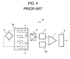
- FIG. 4 is a block diagram of a conventional magnetic sensor.
- a conventional magnetic sensor 10 includes a Hall element 2, a changeover switch circuit 30, an amplifier 4, a sampling circuit 5, a reference voltage circuit 60, a comparator 7, and an output circuit 8.
- the conventional magnetic sensor 10 operates as follows in order to cancel the offset voltage.
- the changeover switch circuit 30 switches current paths between respective two terminals on a diagonal line of the Hall element 2 in a complementary manner between a first period and a second period.
- the output voltage is amplified by the amplifier 4, and is held in a time division manner and averaged by the sampling circuit 5.
- the reference voltage circuit 60 outputs a reference voltage Vref.
- the comparator 7 compares the voltage held in the sampling circuit 5 and the reference voltage Vref, and determines the intensity of the magnetic field.
- the magnetic sensor 10 outputs the determination result via the output circuit 8, thereby outputting a detection signal corresponding to the magnetic field.
- the conventional magnetic sensor 10 operates as described above, and cancels the offset voltages of the Hall
- the offset voltage is higher by several digits than a magnetic field signal voltage.
- the offset voltage is not cancelled mainly due to saturation of the output voltage of the amplifier 4, and magnetic characteristics significantly deteriorate.
- the present invention has been made in order to solve the above-mentioned problem, and provides an inexpensive high-precision magnetic sensor with magnetic characteristics.
- a magnetic sensor according to an exemplary embodiment of the present invention has the following configuration.
- the magnetic sensor includes a changeover switch circuit which causes a current to flow into a first terminal pair of a Hall element and inputs a first differential signal voltage from a second terminal pair thereof during a first period, and which causes a current to flow into the second terminal pair and inputs a second differential signal voltage from the first terminal pair during a second period.
- the changeover switch circuit includes series-transmission switches and cross-transmission switches, the series-transmission switches and the cross-transmission switches being provided in series between terminals of the Hall element and output terminals of the changeover switch circuit.
- the cross-transmission switch is controlled to determine a magnitude of an offset voltage of the Hall element.
- the magnetic sensor of the present invention only by adding a simple circuit, the voltage based on the offset voltages of the Hall element and an amplifier circuit is evaluated. Therefore, an individual having a high offset voltage is identified by binary decision in an inspection process, and hence there is an effect of improving quality of a product.
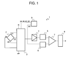
- FIG. 1 is a block diagram of a magnetic sensor according to the embodiment of the present invention.
- a magnetic sensor 1 includes a Hall element 2, a changeover switch circuit 3, an amplifier 4, a sampling circuit 5, a reference voltage circuit 6, a comparator 7, an output circuit 8, and a control circuit 9.
- a current is supplied from a power source terminal to one terminal pair (for example, terminal 21 and terminal 22) on a diagonal line of the Hall element 2, and a differential signal voltage is output from both ends of the other terminal pair thereof (for example, terminal 23 and terminal 24).
- a differential signal voltage of the Hall element 2 is input to the amplifier 4 via the changeover switch circuit 3.
- the changeover switch circuit 3 is controlled by control signals 3A to 3D output from the control circuit 9, and switches between a first period and a second period of control of the Hall element 2.
- the amplifier 4 amplifies the differential signal voltage of the Hall element 2, and outputs a differential signal amplified voltage.
- the reference voltage circuit 6 outputs a reference voltage in accordance with a control signal 6A of the control circuit 9.
- the sampling circuit 5 holds differential signal amplified voltages of the first period and the second period, and outputs an average voltage thereof.
- the comparator 7 compares a magnitude relation between the average voltage and the reference voltage, and outputs a logic signal.
- the control circuit 9 outputs respective control signals to the changeover switch circuit 3, the amplifier 4, and the reference voltage circuit 6.
- the output circuit 8 performs a latch operation and a logical operation based on the logic signal, and outputs a detection signal as a detection signal of the magnetic sensor.
- FIG. 2 is a detailed circuit diagram of the changeover switch circuit 3 of the magnetic sensor according to the embodiment of the present invention.
- the changeover switch circuit 3 includes first to fourth current supply switches 311 to 314, first to fourth series-transmission switches 321 to 324, and first to fourth cross-transmission switches 331 to 334.
- the control signals 3A to 3D are output from the control circuit 9.
- Terminals 301 and 302 are first and second differential signal voltage output terminals.
- the first to fourth series-transmission switches 321 to 324 are switched in association with the first to fourth current supply switches 311 to 314.
- the first to fourth cross-transmission switches 331 to 334 are controlled by the control signals 3C and 3D.
- FIG. 3 is a circuit diagram illustrating one example of the control circuit of the magnetic sensor according to the embodiment of the present invention.
- the control circuit 9 includes an operating state setting circuit 91, a NAND circuit 92, and OR circuits 93, 94, and 95.
- a reference CLK signal is input to the control circuit 9, and the control circuit 9 generates and outputs the control signals 3A, 3B, 3C, and 3D, and the control signal 6A.
- the operating state setting circuit 91 outputs a signal of "H” or "L", and includes a fuse and a pull-down resistor which are connected in series.
- the operating state setting circuit 91 may include a non-volatile memory, or may include an external terminal and input a state setting signal from the exterior. Further, as long as a desired signal is generated, other logic circuits are not limited to the above-mentioned circuit configuration.
- the above-mentioned magnetic sensor 1 operates as follows, and has a function of determining the magnitude of an offset voltage, and a function of determining the intensity of the magnetic field.
- the magnetic sensor 1 has a first operating state and a second operating state depending on the control signals output from the control circuit 9.
- the operating state setting circuit 91 of the control circuit 9 outputs a signal of "H" in the initial state due to the fuse. Therefore, the NAND circuit 92 inverts the reference CLK signal and outputs the inverted signal.
- the control signal 3C is a signal obtained by inverting the reference CLK signal
- the control signal 3D is the same signal as the reference CLK signal.
- This state is the first operating state.
- the operating state setting circuit 91 of the control circuit 9 outputs a signal of "L” due to the pull-down resistor when the fuse is blown. Therefore, output of the NAND circuit 92 is fixed to "H".
- control signals 3C and 3D are respectively fixed to “H” and "L”. This state is the second operating state.
- the control signal 3A is the signal obtained by inverting the reference CLK signal
- the control signal 3B is the same signal as the reference CLK signal.
- the control circuit 9 In the first operating state, the control circuit 9 outputs the control signals 3A and 3C of the signals obtained by inverting the reference CLK signal and the control signals 3B and 3D of the same signals as the reference CLK signal.
- the first and fourth current supply switches 311 and 314 are electrically conductive, a current is supplied to the terminal pair of the terminal 21 and the terminal 22 of the Hall element 2, and the differential signal voltage is output from the terminal pair of the terminal 23 and the terminal 24 thereof.
- the second and third current supply switches 312 and 313 are electrically conductive, a current is supplied to the terminal pair of the terminal 23 and the terminal 24, and the differential signal voltage is output from the terminal pair of the terminal 21 and the terminal 22.
- the second cross-transmission switch 332 and the third cross-transmission switch 333 are electrically conductive, and, during the second period, the first cross-transmission switch 331 and the fourth cross-transmission switch 334 are electrically conductive.
- the first differential signal voltage output terminal 301 is connected to the terminal 24 of the Hall element 2, and the second differential signal voltage output terminal 302 is connected to the terminal 23 of the Hall element 2.
- the first differential signal voltage output terminal 301 is connected to the terminal 21 of the Hall element 2, and the second differential signal voltage output terminal 302 is connected to the terminal 22 of the Hall element 2.
- the output voltages of the first and second differential signal voltage output terminals 301 and 302 are amplified by the amplifier 4, and the amplified voltage is output.
- Vo1 ⁇ 1 and Vo1 ⁇ 2 are respectively obtained from Equations 1 and 2.
- Vo ⁇ 1 ⁇ ⁇ ⁇ 1 VDD / 2 + G ⁇ KH ⁇ Bin + Vos
- Vo ⁇ 1 ⁇ ⁇ ⁇ 2 VDD / 2 + G ⁇ - KH ⁇ Bin + Vos
- VDD represents a power source voltage
- G represents a gain of the amplifier 4
- KH represents a magnetoelectric conversion coefficient of the Hall element 2
- Bin represents a magnetic flux density
- Vos represents an offset voltage included in the output voltage of the amplifier 4.
- the reference voltage to be output is switched by the control signal 6A to a reference voltage Vref2 for determining the offset voltage. Accordingly, the comparator 7 compares the average voltage Vo1 and the reference voltage Vref2 to determine the magnitude of the offset voltage Vos, and the output circuit 8 outputs the result of the determination.
- the magnitude of the offset voltage Vos of the magnetic sensor 1 is determined. Therefore, in the inspection process, an individual having a high offset voltage Vos, which is a defect in the circuit of the magnetic sensor 1, is sorted out without increasing the circuit scale or using an additional inspection tool.
- the amplifier 4 may be switched by the control signal of the control circuit 9 to have a gain for determining the offset voltage.
- the detection operation of the offset voltage may be optimized.
- the second operating state is a normal operating state, in which the intensity of magnetism is determined.
- the control signals 3C and 3D are respectively fixed to "H” and "L", and hence the first cross-transmission switch 331 and the fourth cross-transmission switch 334 are fixed to be electrically conductive.
- the first and fourth current supply switches 311 and 314 are electrically conductive, a current is supplied to the terminal pair of the terminal 21 and the terminal 22 of the Hall element 2, and the differential signal voltage is output from the terminal pair of the terminal 23 and the terminal 24 thereof.
- the second and third current supply switches 312 and 313 are electrically conductive, a current is supplied to the terminal pair of the terminal 23 and the terminal 24, and the differential signal voltage is output from the terminal pair of the terminal 21 and the terminal 22.
- the first differential signal voltage output terminal 301 is connected to the terminal 23 of the Hall element 2, and the second differential signal voltage output terminal 302 is connected to the terminal 24 of the Hall element 2.
- the first differential signal voltage output terminal 301 is connected to the terminal 21 of the Hall element 2, and the second differential signal voltage output terminal 302 is connected to the terminal 22 of the Hall element 2.
- the output voltages of the first and second differential signal voltage output terminals 301 and 302 are amplified by the amplifier 4, and the amplified voltage is output.
- Vo2 ⁇ 1 and Vo2 ⁇ 2 are respectively obtained by Equations 4 and 5.
- Vo ⁇ 2 ⁇ ⁇ ⁇ 2 VDD / 2 + G ⁇ KH ⁇ Bin + Vos
- Vo ⁇ 2 ⁇ ⁇ ⁇ 2 VDD / 2 + G ⁇ KH ⁇ Bin - Vos
- Vo2 VDD / 2 + G ⁇ KH ⁇ Bin
- the comparator 7 compares the average voltage Vo2 obtained from Equation 6 and the reference voltage Vref, and determines the intensity of the magnetic field, thereby outputting the detection signal corresponding to the magnetic field. At that time, the reference voltage circuit 6 is switched to output the normal reference voltage Vref.
- the magnetic sensor according to the embodiment of the present invention evaluates the voltage based on the offset voltages of the Hall element and an amplifier circuit. Therefore, there is identified by binary decision an individual having a high offset voltage liable to generate a magnetic characteristics defect, which is to be an initial defective product. In other words, an individual having a high offset voltage is removed in the inspection process, and hence a high-precision magnetic sensor is provided.
- control circuit 9 In the case of a configuration in which the control circuit 9 inputs a control signal from the exterior, the control signal is input from the exterior, to thereby inspect a product even after product shipment. Therefore, an individual having a higher offset voltage due to change over time is identified.
Landscapes
- Physics & Mathematics (AREA)
- Condensed Matter Physics & Semiconductors (AREA)
- General Physics & Mathematics (AREA)
- Measuring Magnetic Variables (AREA)
- Hall/Mr Elements (AREA)
Abstract
Description
- The present invention relates to a magnetic sensor using a Hall element on a semiconductor substrate, and more particularly, to a characteristic abnormality detection circuit for the magnetic sensor.
- A magnetic sensor is widely used for detecting a movement or a rotation of various movable objects. For example, the magnetic sensor is used to detect opening and closing of a mobile phone, or to detect the rpm of a motor. In recent years, there is used a Hall element formed on a Si substrate, which is inexpensive but has low sensitivity and a high offset voltage. Then, offset voltages of the Hall element and an amplifier are cancelled by signal processing, to thereby realize a magnetic sensor which is inexpensive and has high magnetic detection precision.
-
FIG. 4 is a block diagram of a conventional magnetic sensor. A conventionalmagnetic sensor 10 includes aHall element 2, achangeover switch circuit 30, anamplifier 4, asampling circuit 5, areference voltage circuit 60, acomparator 7, and anoutput circuit 8. The conventionalmagnetic sensor 10 operates as follows in order to cancel the offset voltage. Thechangeover switch circuit 30 switches current paths between respective two terminals on a diagonal line of theHall element 2 in a complementary manner between a first period and a second period. The output voltage is amplified by theamplifier 4, and is held in a time division manner and averaged by thesampling circuit 5. Thereference voltage circuit 60 outputs a reference voltage Vref. Thecomparator 7 compares the voltage held in thesampling circuit 5 and the reference voltage Vref, and determines the intensity of the magnetic field. Themagnetic sensor 10 outputs the determination result via theoutput circuit 8, thereby outputting a detection signal corresponding to the magnetic field. The conventionalmagnetic sensor 10 operates as described above, and cancels the offset voltages of the Hall element and the amplifier by signal processing. - However, when Si is used as a material for the
Hall element 2, the offset voltage is higher by several digits than a magnetic field signal voltage. There has been a problem in that, when the offset voltage is high, the offset voltage is not cancelled mainly due to saturation of the output voltage of theamplifier 4, and magnetic characteristics significantly deteriorate. - The present invention has been made in order to solve the above-mentioned problem, and provides an inexpensive high-precision magnetic sensor with magnetic characteristics.
- In order to solve the conventional problem, a magnetic sensor according to an exemplary embodiment of the present invention has the following configuration.
- The magnetic sensor includes a changeover switch circuit which causes a current to flow into a first terminal pair of a Hall element and inputs a first differential signal voltage from a second terminal pair thereof during a first period, and which causes a current to flow into the second terminal pair and inputs a second differential signal voltage from the first terminal pair during a second period. The changeover switch circuit includes series-transmission switches and cross-transmission switches, the series-transmission switches and the cross-transmission switches being provided in series between terminals of the Hall element and output terminals of the changeover switch circuit. The cross-transmission switch is controlled to determine a magnitude of an offset voltage of the Hall element.
- According to the magnetic sensor of the present invention, only by adding a simple circuit, the voltage based on the offset voltages of the Hall element and an amplifier circuit is evaluated. Therefore, an individual having a high offset voltage is identified by binary decision in an inspection process, and hence there is an effect of improving quality of a product.
- In the accompanying drawings:
-
FIG. 1 is a block diagram of a magnetic sensor according to an embodiment of the present invention; -
FIG. 2 is a detailed circuit diagram of a changeover switch circuit of the magnetic sensor according to the embodiment of the present invention; -
FIG. 3 is a circuit diagram illustrating one example of a control circuit of the magnetic sensor according to the embodiment of the present invention; and -
FIG. 4 is a block diagram of a conventional magnetic sensor. - In the following, an embodiment of the present invention is described with reference to the attached drawings.
-
FIG. 1 is a block diagram of a magnetic sensor according to the embodiment of the present invention. - A
magnetic sensor 1 according to the embodiment of the present invention includes aHall element 2, achangeover switch circuit 3, anamplifier 4, asampling circuit 5, areference voltage circuit 6, acomparator 7, anoutput circuit 8, and acontrol circuit 9. - Via the
changeover switch circuit 3, a current is supplied from a power source terminal to one terminal pair (for example,terminal 21 and terminal 22) on a diagonal line of theHall element 2, and a differential signal voltage is output from both ends of the other terminal pair thereof (for example,terminal 23 and terminal 24). A differential signal voltage of theHall element 2 is input to theamplifier 4 via thechangeover switch circuit 3. Thechangeover switch circuit 3 is controlled bycontrol signals 3A to 3D output from thecontrol circuit 9, and switches between a first period and a second period of control of theHall element 2. Theamplifier 4 amplifies the differential signal voltage of theHall element 2, and outputs a differential signal amplified voltage. Thereference voltage circuit 6 outputs a reference voltage in accordance with acontrol signal 6A of thecontrol circuit 9. Thesampling circuit 5 holds differential signal amplified voltages of the first period and the second period, and outputs an average voltage thereof. Thecomparator 7 compares a magnitude relation between the average voltage and the reference voltage, and outputs a logic signal. Thecontrol circuit 9 outputs respective control signals to thechangeover switch circuit 3, theamplifier 4, and thereference voltage circuit 6. Theoutput circuit 8 performs a latch operation and a logical operation based on the logic signal, and outputs a detection signal as a detection signal of the magnetic sensor. -
FIG. 2 is a detailed circuit diagram of thechangeover switch circuit 3 of the magnetic sensor according to the embodiment of the present invention. - The
changeover switch circuit 3 includes first to fourthcurrent supply switches 311 to 314, first to fourth series-transmission switches 321 to 324, and first tofourth cross-transmission switches 331 to 334. Thecontrol signals 3A to 3D are output from thecontrol circuit 9.Terminals current supply switches 311 to 314 are respectively "L" and "H", that is, a period during which a current is supplied to theterminal 21 and theterminal 22 of theHall element 2, is set as the first period, and a period during which thecontrol signals terminal 23 and theterminal 24 of theHall element 2, is set as the second period. The first to fourth series-transmission switches 321 to 324 are switched in association with the first to fourthcurrent supply switches 311 to 314. The first tofourth cross-transmission switches 331 to 334 are controlled by thecontrol signals -
FIG. 3 is a circuit diagram illustrating one example of the control circuit of the magnetic sensor according to the embodiment of the present invention. Thecontrol circuit 9 includes an operatingstate setting circuit 91, aNAND circuit 92, andOR circuits control circuit 9, and thecontrol circuit 9 generates and outputs thecontrol signals control signal 6A. The operating state settingcircuit 91 outputs a signal of "H" or "L", and includes a fuse and a pull-down resistor which are connected in series. For example, the operatingstate setting circuit 91 may include a non-volatile memory, or may include an external terminal and input a state setting signal from the exterior. Further, as long as a desired signal is generated, other logic circuits are not limited to the above-mentioned circuit configuration. - The above-mentioned
magnetic sensor 1 operates as follows, and has a function of determining the magnitude of an offset voltage, and a function of determining the intensity of the magnetic field. - The
magnetic sensor 1 according to the embodiment of the present invention has a first operating state and a second operating state depending on the control signals output from thecontrol circuit 9. The operating state settingcircuit 91 of thecontrol circuit 9 outputs a signal of "H" in the initial state due to the fuse. Therefore, theNAND circuit 92 inverts the reference CLK signal and outputs the inverted signal. In other words, thecontrol signal 3C is a signal obtained by inverting the reference CLK signal, and thecontrol signal 3D is the same signal as the reference CLK signal. This state is the first operating state. The operatingstate setting circuit 91 of thecontrol circuit 9 outputs a signal of "L" due to the pull-down resistor when the fuse is blown. Therefore, output of theNAND circuit 92 is fixed to "H". In other words, the control signals 3C and 3D are respectively fixed to "H" and "L". This state is the second operating state. In both operating states, thecontrol signal 3A is the signal obtained by inverting the reference CLK signal, and thecontrol signal 3B is the same signal as the reference CLK signal. - Description is given first of the first operating state. In the first operating state, the magnitude of the offset voltage of the
magnetic sensor 1 is determined. - In the first operating state, the
control circuit 9 outputs the control signals 3A and 3C of the signals obtained by inverting the reference CLK signal and thecontrol signals terminal 22 of theHall element 2, and the differential signal voltage is output from the terminal pair of the terminal 23 and theterminal 24 thereof. During the second period, the second and third current supply switches 312 and 313 are electrically conductive, a current is supplied to the terminal pair of the terminal 23 and the terminal 24, and the differential signal voltage is output from the terminal pair of the terminal 21 and the terminal 22. During the first period, the secondcross-transmission switch 332 and the thirdcross-transmission switch 333 are electrically conductive, and, during the second period, the firstcross-transmission switch 331 and the fourthcross-transmission switch 334 are electrically conductive. - Therefore, during the first period, the first differential signal
voltage output terminal 301 is connected to theterminal 24 of theHall element 2, and the second differential signalvoltage output terminal 302 is connected to theterminal 23 of theHall element 2. During the second period, the first differential signalvoltage output terminal 301 is connected to theterminal 21 of theHall element 2, and the second differential signalvoltage output terminal 302 is connected to theterminal 22 of theHall element 2. The output voltages of the first and second differential signalvoltage output terminals amplifier 4, and the amplified voltage is output. - Accordingly, when a differential signal amplified voltage output from the
amplifier 4 during the first period is set as Vo1Φ1 and a differential signal amplified voltage output from theamplifier 4 during the second period is set as Vo1Φ2, Vo1Φ1 and Vo1Φ2 are respectively obtained fromEquations 

where VDD represents a power source voltage, G represents a gain of theamplifier 4, KH represents a magnetoelectric conversion coefficient of theHall element 2, Bin represents a magnetic flux density, and Vos represents an offset voltage included in the output voltage of theamplifier 4. - Therefore, an average voltage Vol, which is obtained by averaging the differential signal amplified voltages Vo1Φ1 and Vo1Φ2 by the
sampling circuit 5, is obtained fromEquation 3.
- At that time, in the
reference voltage circuit 6, the reference voltage to be output is switched by thecontrol signal 6A to a reference voltage Vref2 for determining the offset voltage. Accordingly, thecomparator 7 compares the average voltage Vo1 and the reference voltage Vref2 to determine the magnitude of the offset voltage Vos, and theoutput circuit 8 outputs the result of the determination. - In this way, in the first operating state, the magnitude of the offset voltage Vos of the
magnetic sensor 1 is determined. Therefore, in the inspection process, an individual having a high offset voltage Vos, which is a defect in the circuit of themagnetic sensor 1, is sorted out without increasing the circuit scale or using an additional inspection tool. - The
amplifier 4 may be switched by the control signal of thecontrol circuit 9 to have a gain for determining the offset voltage. By appropriately adjusting the reference voltage of thereference voltage circuit 6 and the gain of theamplifier 4, the detection operation of the offset voltage may be optimized. - Description is given next of the second operating state. The second operating state is a normal operating state, in which the intensity of magnetism is determined.
- In the second operating state, the control signals 3C and 3D are respectively fixed to "H" and "L", and hence the first
cross-transmission switch 331 and the fourthcross-transmission switch 334 are fixed to be electrically conductive. During the first period, the first and fourth current supply switches 311 and 314 are electrically conductive, a current is supplied to the terminal pair of the terminal 21 and theterminal 22 of theHall element 2, and the differential signal voltage is output from the terminal pair of the terminal 23 and theterminal 24 thereof. During the second period, the second and third current supply switches 312 and 313 are electrically conductive, a current is supplied to the terminal pair of the terminal 23 and the terminal 24, and the differential signal voltage is output from the terminal pair of the terminal 21 and the terminal 22. Therefore, during the first period, the first differential signalvoltage output terminal 301 is connected to theterminal 23 of theHall element 2, and the second differential signalvoltage output terminal 302 is connected to theterminal 24 of theHall element 2. During the second period, the first differential signalvoltage output terminal 301 is connected to theterminal 21 of theHall element 2, and the second differential signalvoltage output terminal 302 is connected to theterminal 22 of theHall element 2. The output voltages of the first and second differential signalvoltage output terminals amplifier 4, and the amplified voltage is output. - When a differential signal amplified voltage output from the
amplifier 4 during the first period is set as Vo2Φ1 and a differential signal amplified voltage output from theamplifier 4 during the second period is set as Vo2Φ2, Vo2Φ1 and Vo2Φ2 are respectively obtained byEquations 

- Therefore, an average voltage Vo2, which is obtained by averaging the differential signal amplified voltages Vo2Φ1 and Vo2Φ2 by the
sampling circuit 5, is obtained fromEquation 6.
- From
Equation 6, it is understood that the offset voltage Vos is cancelled in the average voltage Vo2. Thecomparator 7 compares the average voltage Vo2 obtained fromEquation 6 and the reference voltage Vref, and determines the intensity of the magnetic field, thereby outputting the detection signal corresponding to the magnetic field. At that time, thereference voltage circuit 6 is switched to output the normal reference voltage Vref. - As described above, in the first operating state, the magnetic sensor according to the embodiment of the present invention evaluates the voltage based on the offset voltages of the Hall element and an amplifier circuit. Therefore, there is identified by binary decision an individual having a high offset voltage liable to generate a magnetic characteristics defect, which is to be an initial defective product. In other words, an individual having a high offset voltage is removed in the inspection process, and hence a high-precision magnetic sensor is provided.
- In the case of a configuration in which the
control circuit 9 inputs a control signal from the exterior, the control signal is input from the exterior, to thereby inspect a product even after product shipment. Therefore, an individual having a higher offset voltage due to change over time is identified.
Claims (5)
- A magnetic sensor, comprising:a Hall element;a changeover switch circuit which causes a current to flow into a first terminal pair of the Hall element and inputs a first differential signal voltage from a second terminal pair of the Hall element during a first period, and which causes a current to flow into the second terminal pair and inputs a second differential signal voltage from the first terminal pair during a second period;an amplifier which outputs a first differential signal amplified voltage and a second differential signal amplified voltage, the first differential signal amplified voltage and the second differential signal amplified voltage being respectively obtained by amplifying the first differential signal voltage and the second differential signal voltage which are input via the changeover switch circuit;a sampling circuit which holds the first differential signal amplified voltage and the second differential signal amplified voltage input from the amplifier, and which outputs an average voltage of the first differential signal amplified voltage and the second differential signal amplified voltage;a reference voltage circuit which generates a reference voltage;a comparator which compares the average voltage output from the sampling circuit and the reference voltage output from the reference voltage circuit; anda control circuit which outputs a control signal to control the changeover switch circuit;wherein the changeover switch circuit comprises series-transmission switches and cross-transmission switches, the series-transmission switches and the cross-transmission switches being provided in series between input terminals connected to terminals of the Hall element and output terminals of the changeover switch circuit.
- A magnetic sensor according to claim 1, wherein:the cross-transmission switch is controlled to cross-transmit a signal in any one of the first period and the second period in a first operating state;the cross-transmission switch is controlled not to cross-transmit a signal in any one of the first period and the second period in a second operating state; anda magnitude of an offset voltage included in the average voltage is determined in the first operating state.
- A magnetic sensor according to claim 2, wherein the control circuit comprises a fuse, and switches between the first operating state and the second operating state depending on presence and absence of the fuse.
- A magnetic sensor according to claim 2, wherein the control circuit comprises a non-volatile memory, and switches between the first operating state and the second operating state depending on data of the non-volatile memory.
- A magnetic sensor according to claim 2, wherein the control circuit comprises a state setting terminal, and switches between the first operating state and the second operating state depending on a signal input to the state setting terminal.
Applications Claiming Priority (2)
| Application Number | Priority Date | Filing Date | Title |
|---|---|---|---|
| JP2012130161A JP6004758B2 (en) | 2012-06-07 | 2012-06-07 | Magnetic sensor |
| PCT/JP2013/060882 WO2013183355A1 (en) | 2012-06-07 | 2013-04-11 | Magnetic sensor |
Publications (3)
| Publication Number | Publication Date |
|---|---|
| EP2860541A1 true EP2860541A1 (en) | 2015-04-15 |
| EP2860541A4 EP2860541A4 (en) | 2016-03-02 |
| EP2860541B1 EP2860541B1 (en) | 2016-12-21 |
Family
ID=49711756
Family Applications (1)
| Application Number | Title | Priority Date | Filing Date |
|---|---|---|---|
| EP13800245.6A Not-in-force EP2860541B1 (en) | 2012-06-07 | 2013-04-11 | Magnetic sensor |
Country Status (7)
| Country | Link |
|---|---|
| US (1) | US9523743B2 (en) |
| EP (1) | EP2860541B1 (en) |
| JP (1) | JP6004758B2 (en) |
| KR (1) | KR101972629B1 (en) |
| CN (1) | CN104364670B (en) |
| TW (1) | TWI567406B (en) |
| WO (1) | WO2013183355A1 (en) |
Families Citing this family (5)
| Publication number | Priority date | Publication date | Assignee | Title |
|---|---|---|---|---|
| CN105899964B (en) * | 2014-01-23 | 2019-09-24 | 三菱电机株式会社 | Magnetic detection device |
| KR101905341B1 (en) | 2014-09-04 | 2018-10-05 | 더 팀켄 컴퍼니 | Hall effect sensor circuit with offset compensation |
| JP6721910B2 (en) * | 2016-07-29 | 2020-07-15 | 株式会社Terada | Current measuring device |
| JP7535954B2 (en) * | 2020-03-13 | 2024-08-19 | エイブリック株式会社 | Semiconductor Device |
| JP7641796B2 (en) * | 2021-03-30 | 2025-03-07 | エイブリック株式会社 | Sensor Device |
Family Cites Families (15)
| Publication number | Priority date | Publication date | Assignee | Title |
|---|---|---|---|---|
| DE59108800D1 (en) * | 1991-12-21 | 1997-08-28 | Itt Ind Gmbh Deutsche | Offset compensated Hall sensor |
| JP3887275B2 (en) * | 2002-07-03 | 2007-02-28 | 東光株式会社 | Sensor circuit |
| JP4641775B2 (en) * | 2004-09-29 | 2011-03-02 | ルネサスエレクトロニクス株式会社 | Semiconductor integrated circuit for magnetic detection and electronic component mounted therewith |
| EP1850143A1 (en) | 2005-02-08 | 2007-10-31 | Rohm Co., Ltd. | Magnetic sensor circuit and portable terminal provided with such magnetic sensor circuit |
| JP2008032424A (en) * | 2006-07-26 | 2008-02-14 | Rohm Co Ltd | Sensor circuit, semiconductor device, electronic equipment |
| JP4922204B2 (en) * | 2007-02-19 | 2012-04-25 | 株式会社東芝 | Signal detection circuit |
| JP4897585B2 (en) * | 2007-06-22 | 2012-03-14 | ローム株式会社 | Magnetic sensor circuit and electronic device using the same |
| CN101340168A (en) * | 2007-07-03 | 2009-01-07 | 台达电子工业股份有限公司 | Motor control device and method thereof |
| JP5052982B2 (en) * | 2007-07-25 | 2012-10-17 | セイコーインスツル株式会社 | Magnetic sensor circuit |
| JP5225938B2 (en) * | 2009-06-08 | 2013-07-03 | セイコーインスツル株式会社 | Magnetic sensor device |
| JP2010281764A (en) * | 2009-06-08 | 2010-12-16 | Sanyo Electric Co Ltd | Offset cancel circuit |
| JP2011075338A (en) * | 2009-09-29 | 2011-04-14 | Seiko Instruments Inc | Magnetic sensor circuit |
| JP5281556B2 (en) * | 2009-12-07 | 2013-09-04 | セイコーインスツル株式会社 | Physical quantity sensor |
| CN101782634B (en) * | 2010-02-23 | 2013-07-10 | 南京大学 | On-chip all-in-one micro integrated magnetic sensor |
| US8633687B2 (en) * | 2010-12-21 | 2014-01-21 | Robert Bosch Gmbh | Hall Effect sensor with reduced offset |
-
2012
- 2012-06-07 JP JP2012130161A patent/JP6004758B2/en active Active
-
2013
- 2013-04-11 CN CN201380029928.6A patent/CN104364670B/en not_active Expired - Fee Related
- 2013-04-11 KR KR1020147034110A patent/KR101972629B1/en not_active Expired - Fee Related
- 2013-04-11 WO PCT/JP2013/060882 patent/WO2013183355A1/en not_active Ceased
- 2013-04-11 EP EP13800245.6A patent/EP2860541B1/en not_active Not-in-force
- 2013-04-19 TW TW102113962A patent/TWI567406B/en not_active IP Right Cessation
-
2014
- 2014-12-04 US US14/560,806 patent/US9523743B2/en not_active Expired - Fee Related
Also Published As
| Publication number | Publication date |
|---|---|
| EP2860541B1 (en) | 2016-12-21 |
| EP2860541A4 (en) | 2016-03-02 |
| US20150084620A1 (en) | 2015-03-26 |
| TWI567406B (en) | 2017-01-21 |
| JP2013253886A (en) | 2013-12-19 |
| WO2013183355A1 (en) | 2013-12-12 |
| JP6004758B2 (en) | 2016-10-12 |
| TW201350893A (en) | 2013-12-16 |
| CN104364670B (en) | 2016-09-14 |
| CN104364670A (en) | 2015-02-18 |
| US9523743B2 (en) | 2016-12-20 |
| KR101972629B1 (en) | 2019-04-25 |
| KR20150023348A (en) | 2015-03-05 |
Similar Documents
| Publication | Publication Date | Title |
|---|---|---|
| US8274281B2 (en) | Magnetic sensor circuit for detecting and monitoring a magnetic field | |
| US9523743B2 (en) | Magnetic sensor capable of identifying an individual having a high offset voltage | |
| US10156589B2 (en) | Sensor module that switches plural sensors capable of measuring different ranges to extend dynamic range | |
| CN104254784B (en) | Sensor device | |
| US9128127B2 (en) | Sensor device | |
| CN101738588B (en) | Sensor circuit | |
| US9638761B2 (en) | Magnetic sensor circuit with power supply fluctuation detection | |
| TW201443465A (en) | Magnetic sensing apparatus | |
| JP6339890B2 (en) | Current sensor | |
| US9322672B2 (en) | Magnetic sensor device | |
| US10914610B2 (en) | Zero cross detection circuit and sensor device | |
| JPWO2016021480A1 (en) | Current sensor | |
| JP2017166975A (en) | Open/short inspection circuit and load drive device | |
| US8564350B2 (en) | Hysteresis device | |
| JP6192251B2 (en) | Current sensor | |
| TWI545890B (en) | Electronic device and comparator thereof | |
| CN104569563A (en) | High-speed serial data envelope detector | |
| US7332958B2 (en) | Analog-differential-circuit test device | |
| JP2012088151A (en) | Bridge circuit |
Legal Events
| Date | Code | Title | Description |
|---|---|---|---|
| PUAI | Public reference made under article 153(3) epc to a published international application that has entered the european phase |
Free format text: ORIGINAL CODE: 0009012 |
|
| 17P | Request for examination filed |
Effective date: 20150107 |
|
| AK | Designated contracting states |
Kind code of ref document: A1 Designated state(s): AL AT BE BG CH CY CZ DE DK EE ES FI FR GB GR HR HU IE IS IT LI LT LU LV MC MK MT NL NO PL PT RO RS SE SI SK SM TR |
|
| AX | Request for extension of the european patent |
Extension state: BA ME |
|
| DAX | Request for extension of the european patent (deleted) | ||
| RIN1 | Information on inventor provided before grant (corrected) |
Inventor name: HIKICHI, TOMOKI Inventor name: ARIYAMA, MINORU |
|
| RA4 | Supplementary search report drawn up and despatched (corrected) |
Effective date: 20160201 |
|
| RIC1 | Information provided on ipc code assigned before grant |
Ipc: G01R 33/07 20060101AFI20160126BHEP |
|
| RAP1 | Party data changed (applicant data changed or rights of an application transferred) |
Owner name: SII SEMICONDUCTOR CORPORATION |
|
| GRAP | Despatch of communication of intention to grant a patent |
Free format text: ORIGINAL CODE: EPIDOSNIGR1 |
|
| INTG | Intention to grant announced |
Effective date: 20160929 |
|
| RIN1 | Information on inventor provided before grant (corrected) |
Inventor name: ARIYAMA, MINORU Inventor name: HIKICHI, TOMOKI |
|
| GRAS | Grant fee paid |
Free format text: ORIGINAL CODE: EPIDOSNIGR3 |
|
| GRAA | (expected) grant |
Free format text: ORIGINAL CODE: 0009210 |
|
| AK | Designated contracting states |
Kind code of ref document: B1 Designated state(s): AL AT BE BG CH CY CZ DE DK EE ES FI FR GB GR HR HU IE IS IT LI LT LU LV MC MK MT NL NO PL PT RO RS SE SI SK SM TR |
|
| REG | Reference to a national code |
Ref country code: GB Ref legal event code: FG4D |
|
| REG | Reference to a national code |
Ref country code: CH Ref legal event code: EP |
|
| REG | Reference to a national code |
Ref country code: IE Ref legal event code: FG4D |
|
| REG | Reference to a national code |
Ref country code: AT Ref legal event code: REF Ref document number: 855947 Country of ref document: AT Kind code of ref document: T Effective date: 20170115 |
|
| REG | Reference to a national code |
Ref country code: DE Ref legal event code: R096 Ref document number: 602013015717 Country of ref document: DE |
|
| PG25 | Lapsed in a contracting state [announced via postgrant information from national office to epo] |
Ref country code: LV Free format text: LAPSE BECAUSE OF FAILURE TO SUBMIT A TRANSLATION OF THE DESCRIPTION OR TO PAY THE FEE WITHIN THE PRESCRIBED TIME-LIMIT Effective date: 20161221 |
|
| REG | Reference to a national code |
Ref country code: FR Ref legal event code: PLFP Year of fee payment: 5 |
|
| REG | Reference to a national code |
Ref country code: LT Ref legal event code: MG4D |
|
| REG | Reference to a national code |
Ref country code: NL Ref legal event code: MP Effective date: 20161221 |
|
| PG25 | Lapsed in a contracting state [announced via postgrant information from national office to epo] |
Ref country code: SE Free format text: LAPSE BECAUSE OF FAILURE TO SUBMIT A TRANSLATION OF THE DESCRIPTION OR TO PAY THE FEE WITHIN THE PRESCRIBED TIME-LIMIT Effective date: 20161221 Ref country code: NO Free format text: LAPSE BECAUSE OF FAILURE TO SUBMIT A TRANSLATION OF THE DESCRIPTION OR TO PAY THE FEE WITHIN THE PRESCRIBED TIME-LIMIT Effective date: 20170321 Ref country code: LT Free format text: LAPSE BECAUSE OF FAILURE TO SUBMIT A TRANSLATION OF THE DESCRIPTION OR TO PAY THE FEE WITHIN THE PRESCRIBED TIME-LIMIT Effective date: 20161221 Ref country code: GR Free format text: LAPSE BECAUSE OF FAILURE TO SUBMIT A TRANSLATION OF THE DESCRIPTION OR TO PAY THE FEE WITHIN THE PRESCRIBED TIME-LIMIT Effective date: 20170322 |
|
| REG | Reference to a national code |
Ref country code: AT Ref legal event code: MK05 Ref document number: 855947 Country of ref document: AT Kind code of ref document: T Effective date: 20161221 |
|
| PG25 | Lapsed in a contracting state [announced via postgrant information from national office to epo] |
Ref country code: FI Free format text: LAPSE BECAUSE OF FAILURE TO SUBMIT A TRANSLATION OF THE DESCRIPTION OR TO PAY THE FEE WITHIN THE PRESCRIBED TIME-LIMIT Effective date: 20161221 Ref country code: RS Free format text: LAPSE BECAUSE OF FAILURE TO SUBMIT A TRANSLATION OF THE DESCRIPTION OR TO PAY THE FEE WITHIN THE PRESCRIBED TIME-LIMIT Effective date: 20161221 Ref country code: HR Free format text: LAPSE BECAUSE OF FAILURE TO SUBMIT A TRANSLATION OF THE DESCRIPTION OR TO PAY THE FEE WITHIN THE PRESCRIBED TIME-LIMIT Effective date: 20161221 |
|
| PG25 | Lapsed in a contracting state [announced via postgrant information from national office to epo] |
Ref country code: NL Free format text: LAPSE BECAUSE OF FAILURE TO SUBMIT A TRANSLATION OF THE DESCRIPTION OR TO PAY THE FEE WITHIN THE PRESCRIBED TIME-LIMIT Effective date: 20161221 |
|
| PG25 | Lapsed in a contracting state [announced via postgrant information from national office to epo] |
Ref country code: SK Free format text: LAPSE BECAUSE OF FAILURE TO SUBMIT A TRANSLATION OF THE DESCRIPTION OR TO PAY THE FEE WITHIN THE PRESCRIBED TIME-LIMIT Effective date: 20161221 Ref country code: RO Free format text: LAPSE BECAUSE OF FAILURE TO SUBMIT A TRANSLATION OF THE DESCRIPTION OR TO PAY THE FEE WITHIN THE PRESCRIBED TIME-LIMIT Effective date: 20161221 Ref country code: EE Free format text: LAPSE BECAUSE OF FAILURE TO SUBMIT A TRANSLATION OF THE DESCRIPTION OR TO PAY THE FEE WITHIN THE PRESCRIBED TIME-LIMIT Effective date: 20161221 Ref country code: CZ Free format text: LAPSE BECAUSE OF FAILURE TO SUBMIT A TRANSLATION OF THE DESCRIPTION OR TO PAY THE FEE WITHIN THE PRESCRIBED TIME-LIMIT Effective date: 20161221 Ref country code: IS Free format text: LAPSE BECAUSE OF FAILURE TO SUBMIT A TRANSLATION OF THE DESCRIPTION OR TO PAY THE FEE WITHIN THE PRESCRIBED TIME-LIMIT Effective date: 20170421 |
|
| PG25 | Lapsed in a contracting state [announced via postgrant information from national office to epo] |
Ref country code: AT Free format text: LAPSE BECAUSE OF FAILURE TO SUBMIT A TRANSLATION OF THE DESCRIPTION OR TO PAY THE FEE WITHIN THE PRESCRIBED TIME-LIMIT Effective date: 20161221 Ref country code: BG Free format text: LAPSE BECAUSE OF FAILURE TO SUBMIT A TRANSLATION OF THE DESCRIPTION OR TO PAY THE FEE WITHIN THE PRESCRIBED TIME-LIMIT Effective date: 20170321 Ref country code: PT Free format text: LAPSE BECAUSE OF FAILURE TO SUBMIT A TRANSLATION OF THE DESCRIPTION OR TO PAY THE FEE WITHIN THE PRESCRIBED TIME-LIMIT Effective date: 20170421 Ref country code: IT Free format text: LAPSE BECAUSE OF FAILURE TO SUBMIT A TRANSLATION OF THE DESCRIPTION OR TO PAY THE FEE WITHIN THE PRESCRIBED TIME-LIMIT Effective date: 20161221 Ref country code: BE Free format text: LAPSE BECAUSE OF FAILURE TO SUBMIT A TRANSLATION OF THE DESCRIPTION OR TO PAY THE FEE WITHIN THE PRESCRIBED TIME-LIMIT Effective date: 20161221 Ref country code: SM Free format text: LAPSE BECAUSE OF FAILURE TO SUBMIT A TRANSLATION OF THE DESCRIPTION OR TO PAY THE FEE WITHIN THE PRESCRIBED TIME-LIMIT Effective date: 20161221 Ref country code: PL Free format text: LAPSE BECAUSE OF FAILURE TO SUBMIT A TRANSLATION OF THE DESCRIPTION OR TO PAY THE FEE WITHIN THE PRESCRIBED TIME-LIMIT Effective date: 20161221 Ref country code: ES Free format text: LAPSE BECAUSE OF FAILURE TO SUBMIT A TRANSLATION OF THE DESCRIPTION OR TO PAY THE FEE WITHIN THE PRESCRIBED TIME-LIMIT Effective date: 20161221 |
|
| REG | Reference to a national code |
Ref country code: DE Ref legal event code: R097 Ref document number: 602013015717 Country of ref document: DE |
|
| PLBE | No opposition filed within time limit |
Free format text: ORIGINAL CODE: 0009261 |
|
| STAA | Information on the status of an ep patent application or granted ep patent |
Free format text: STATUS: NO OPPOSITION FILED WITHIN TIME LIMIT |
|
| 26N | No opposition filed |
Effective date: 20170922 |
|
| PG25 | Lapsed in a contracting state [announced via postgrant information from national office to epo] |
Ref country code: DK Free format text: LAPSE BECAUSE OF FAILURE TO SUBMIT A TRANSLATION OF THE DESCRIPTION OR TO PAY THE FEE WITHIN THE PRESCRIBED TIME-LIMIT Effective date: 20161221 |
|
| REG | Reference to a national code |
Ref country code: CH Ref legal event code: PL |
|
| GBPC | Gb: european patent ceased through non-payment of renewal fee |
Effective date: 20170411 |
|
| REG | Reference to a national code |
Ref country code: IE Ref legal event code: MM4A |
|
| PG25 | Lapsed in a contracting state [announced via postgrant information from national office to epo] |
Ref country code: MC Free format text: LAPSE BECAUSE OF FAILURE TO SUBMIT A TRANSLATION OF THE DESCRIPTION OR TO PAY THE FEE WITHIN THE PRESCRIBED TIME-LIMIT Effective date: 20161221 |
|
| PG25 | Lapsed in a contracting state [announced via postgrant information from national office to epo] |
Ref country code: SI Free format text: LAPSE BECAUSE OF FAILURE TO SUBMIT A TRANSLATION OF THE DESCRIPTION OR TO PAY THE FEE WITHIN THE PRESCRIBED TIME-LIMIT Effective date: 20161221 Ref country code: GB Free format text: LAPSE BECAUSE OF NON-PAYMENT OF DUE FEES Effective date: 20170411 Ref country code: LU Free format text: LAPSE BECAUSE OF NON-PAYMENT OF DUE FEES Effective date: 20170411 Ref country code: LI Free format text: LAPSE BECAUSE OF NON-PAYMENT OF DUE FEES Effective date: 20170430 Ref country code: CH Free format text: LAPSE BECAUSE OF NON-PAYMENT OF DUE FEES Effective date: 20170430 |
|
| REG | Reference to a national code |
Ref country code: FR Ref legal event code: PLFP Year of fee payment: 6 |
|
| PG25 | Lapsed in a contracting state [announced via postgrant information from national office to epo] |
Ref country code: IE Free format text: LAPSE BECAUSE OF NON-PAYMENT OF DUE FEES Effective date: 20170411 |
|
| REG | Reference to a national code |
Ref country code: DE Ref legal event code: R081 Ref document number: 602013015717 Country of ref document: DE Owner name: ABLIC INC., JP Free format text: FORMER OWNER: SII SEMICONDUCTOR CORPORATION, CHIBA-SHI, CHIBA, JP |
|
| PG25 | Lapsed in a contracting state [announced via postgrant information from national office to epo] |
Ref country code: MT Free format text: LAPSE BECAUSE OF NON-PAYMENT OF DUE FEES Effective date: 20170411 |
|
| PG25 | Lapsed in a contracting state [announced via postgrant information from national office to epo] |
Ref country code: HU Free format text: LAPSE BECAUSE OF FAILURE TO SUBMIT A TRANSLATION OF THE DESCRIPTION OR TO PAY THE FEE WITHIN THE PRESCRIBED TIME-LIMIT; INVALID AB INITIO Effective date: 20130411 |
|
| PG25 | Lapsed in a contracting state [announced via postgrant information from national office to epo] |
Ref country code: CY Free format text: LAPSE BECAUSE OF FAILURE TO SUBMIT A TRANSLATION OF THE DESCRIPTION OR TO PAY THE FEE WITHIN THE PRESCRIBED TIME-LIMIT Effective date: 20161221 |
|
| PG25 | Lapsed in a contracting state [announced via postgrant information from national office to epo] |
Ref country code: MK Free format text: LAPSE BECAUSE OF FAILURE TO SUBMIT A TRANSLATION OF THE DESCRIPTION OR TO PAY THE FEE WITHIN THE PRESCRIBED TIME-LIMIT Effective date: 20161221 |
|
| PG25 | Lapsed in a contracting state [announced via postgrant information from national office to epo] |
Ref country code: TR Free format text: LAPSE BECAUSE OF FAILURE TO SUBMIT A TRANSLATION OF THE DESCRIPTION OR TO PAY THE FEE WITHIN THE PRESCRIBED TIME-LIMIT Effective date: 20161221 |
|
| PGFP | Annual fee paid to national office [announced via postgrant information from national office to epo] |
Ref country code: FR Payment date: 20200312 Year of fee payment: 8 |
|
| PG25 | Lapsed in a contracting state [announced via postgrant information from national office to epo] |
Ref country code: AL Free format text: LAPSE BECAUSE OF FAILURE TO SUBMIT A TRANSLATION OF THE DESCRIPTION OR TO PAY THE FEE WITHIN THE PRESCRIBED TIME-LIMIT Effective date: 20161221 |
|
| PGFP | Annual fee paid to national office [announced via postgrant information from national office to epo] |
Ref country code: DE Payment date: 20200331 Year of fee payment: 8 |
|
| REG | Reference to a national code |
Ref country code: DE Ref legal event code: R119 Ref document number: 602013015717 Country of ref document: DE |
|
| PG25 | Lapsed in a contracting state [announced via postgrant information from national office to epo] |
Ref country code: FR Free format text: LAPSE BECAUSE OF NON-PAYMENT OF DUE FEES Effective date: 20210430 Ref country code: DE Free format text: LAPSE BECAUSE OF NON-PAYMENT OF DUE FEES Effective date: 20211103 |