EP2858092A1 - Method for manufacturing soi wafer - Google Patents
Method for manufacturing soi wafer Download PDFInfo
- Publication number
- EP2858092A1 EP2858092A1 EP13794721.4A EP13794721A EP2858092A1 EP 2858092 A1 EP2858092 A1 EP 2858092A1 EP 13794721 A EP13794721 A EP 13794721A EP 2858092 A1 EP2858092 A1 EP 2858092A1
- Authority
- EP
- European Patent Office
- Prior art keywords
- wafer
- insulator film
- soi
- bonded
- bond
- Prior art date
- Legal status (The legal status is an assumption and is not a legal conclusion. Google has not performed a legal analysis and makes no representation as to the accuracy of the status listed.)
- Granted
Links
Images

Classifications
-
- H—ELECTRICITY
- H10—SEMICONDUCTOR DEVICES; ELECTRIC SOLID-STATE DEVICES NOT OTHERWISE PROVIDED FOR
- H10D—INORGANIC ELECTRIC SEMICONDUCTOR DEVICES
- H10D86/00—Integrated devices formed in or on insulating or conducting substrates, e.g. formed in silicon-on-insulator [SOI] substrates or on stainless steel or glass substrates
-
- H—ELECTRICITY
- H10—SEMICONDUCTOR DEVICES; ELECTRIC SOLID-STATE DEVICES NOT OTHERWISE PROVIDED FOR
- H10P—GENERIC PROCESSES OR APPARATUS FOR THE MANUFACTURE OR TREATMENT OF DEVICES COVERED BY CLASS H10
- H10P90/00—Preparation of wafers not covered by a single main group of this subclass, e.g. wafer reinforcement
- H10P90/19—Preparing inhomogeneous wafers
- H10P90/1904—Preparing vertically inhomogeneous wafers
- H10P90/1906—Preparing SOI wafers
- H10P90/1914—Preparing SOI wafers using bonding
- H10P90/1916—Preparing SOI wafers using bonding with separation or delamination along an ion implanted layer, e.g. Smart-cut
-
- H—ELECTRICITY
- H10—SEMICONDUCTOR DEVICES; ELECTRIC SOLID-STATE DEVICES NOT OTHERWISE PROVIDED FOR
- H10P—GENERIC PROCESSES OR APPARATUS FOR THE MANUFACTURE OR TREATMENT OF DEVICES COVERED BY CLASS H10
- H10P14/00—Formation of materials, e.g. in the shape of layers or pillars
- H10P14/60—Formation of materials, e.g. in the shape of layers or pillars of insulating materials
-
- H—ELECTRICITY
- H10—SEMICONDUCTOR DEVICES; ELECTRIC SOLID-STATE DEVICES NOT OTHERWISE PROVIDED FOR
- H10P—GENERIC PROCESSES OR APPARATUS FOR THE MANUFACTURE OR TREATMENT OF DEVICES COVERED BY CLASS H10
- H10P30/00—Ion implantation into wafers, substrates or parts of devices
- H10P30/20—Ion implantation into wafers, substrates or parts of devices into semiconductor materials, e.g. for doping
-
- H—ELECTRICITY
- H10—SEMICONDUCTOR DEVICES; ELECTRIC SOLID-STATE DEVICES NOT OTHERWISE PROVIDED FOR
- H10P—GENERIC PROCESSES OR APPARATUS FOR THE MANUFACTURE OR TREATMENT OF DEVICES COVERED BY CLASS H10
- H10P36/00—Gettering within semiconductor bodies
- H10P36/03—Gettering within semiconductor bodies within silicon bodies
- H10P36/07—Gettering within semiconductor bodies within silicon bodies of silicon-on-insulator structures
-
- H—ELECTRICITY
- H10—SEMICONDUCTOR DEVICES; ELECTRIC SOLID-STATE DEVICES NOT OTHERWISE PROVIDED FOR
- H10P—GENERIC PROCESSES OR APPARATUS FOR THE MANUFACTURE OR TREATMENT OF DEVICES COVERED BY CLASS H10
- H10P50/00—Etching of wafers, substrates or parts of devices
-
- H—ELECTRICITY
- H10—SEMICONDUCTOR DEVICES; ELECTRIC SOLID-STATE DEVICES NOT OTHERWISE PROVIDED FOR
- H10P—GENERIC PROCESSES OR APPARATUS FOR THE MANUFACTURE OR TREATMENT OF DEVICES COVERED BY CLASS H10
- H10P50/00—Etching of wafers, substrates or parts of devices
- H10P50/60—Wet etching
- H10P50/64—Wet etching of semiconductor materials
- H10P50/642—Chemical etching
-
- H—ELECTRICITY
- H10—SEMICONDUCTOR DEVICES; ELECTRIC SOLID-STATE DEVICES NOT OTHERWISE PROVIDED FOR
- H10P—GENERIC PROCESSES OR APPARATUS FOR THE MANUFACTURE OR TREATMENT OF DEVICES COVERED BY CLASS H10
- H10P50/00—Etching of wafers, substrates or parts of devices
- H10P50/69—Etching of wafers, substrates or parts of devices using masks for semiconductor materials
- H10P50/691—Etching of wafers, substrates or parts of devices using masks for semiconductor materials for Group V materials or Group III-V materials
- H10P50/692—Etching of wafers, substrates or parts of devices using masks for semiconductor materials for Group V materials or Group III-V materials characterised by their composition, e.g. multilayer masks or materials
-
- H—ELECTRICITY
- H10—SEMICONDUCTOR DEVICES; ELECTRIC SOLID-STATE DEVICES NOT OTHERWISE PROVIDED FOR
- H10P—GENERIC PROCESSES OR APPARATUS FOR THE MANUFACTURE OR TREATMENT OF DEVICES COVERED BY CLASS H10
- H10P50/00—Etching of wafers, substrates or parts of devices
- H10P50/69—Etching of wafers, substrates or parts of devices using masks for semiconductor materials
- H10P50/691—Etching of wafers, substrates or parts of devices using masks for semiconductor materials for Group V materials or Group III-V materials
- H10P50/693—Etching of wafers, substrates or parts of devices using masks for semiconductor materials for Group V materials or Group III-V materials characterised by their size, orientation, disposition, behaviour or shape, in horizontal or vertical plane
- H10P50/695—Etching of wafers, substrates or parts of devices using masks for semiconductor materials for Group V materials or Group III-V materials characterised by their size, orientation, disposition, behaviour or shape, in horizontal or vertical plane characterised by the process involved to create the mask, e.g. lift-off masks or sidewalls or to modify the mask
-
- H—ELECTRICITY
- H10—SEMICONDUCTOR DEVICES; ELECTRIC SOLID-STATE DEVICES NOT OTHERWISE PROVIDED FOR
- H10P—GENERIC PROCESSES OR APPARATUS FOR THE MANUFACTURE OR TREATMENT OF DEVICES COVERED BY CLASS H10
- H10P90/00—Preparation of wafers not covered by a single main group of this subclass, e.g. wafer reinforcement
- H10P90/19—Preparing inhomogeneous wafers
- H10P90/1904—Preparing vertically inhomogeneous wafers
- H10P90/1906—Preparing SOI wafers
- H10P90/1914—Preparing SOI wafers using bonding
-
- H—ELECTRICITY
- H10—SEMICONDUCTOR DEVICES; ELECTRIC SOLID-STATE DEVICES NOT OTHERWISE PROVIDED FOR
- H10P—GENERIC PROCESSES OR APPARATUS FOR THE MANUFACTURE OR TREATMENT OF DEVICES COVERED BY CLASS H10
- H10P90/00—Preparation of wafers not covered by a single main group of this subclass, e.g. wafer reinforcement
- H10P90/19—Preparing inhomogeneous wafers
- H10P90/1904—Preparing vertically inhomogeneous wafers
- H10P90/1906—Preparing SOI wafers
- H10P90/1922—Preparing SOI wafers using silicon etch back techniques, e.g. BESOI or ELTRAN
-
- H—ELECTRICITY
- H10—SEMICONDUCTOR DEVICES; ELECTRIC SOLID-STATE DEVICES NOT OTHERWISE PROVIDED FOR
- H10W—GENERIC PACKAGES, INTERCONNECTIONS, CONNECTORS OR OTHER CONSTRUCTIONAL DETAILS OF DEVICES COVERED BY CLASS H10
- H10W10/00—Isolation regions in semiconductor bodies between components of integrated devices
- H10W10/10—Isolation regions comprising dielectric materials
- H10W10/181—Semiconductor-on-insulator [SOI] isolation regions, e.g. buried oxide regions of SOI wafers
-
- H—ELECTRICITY
- H10—SEMICONDUCTOR DEVICES; ELECTRIC SOLID-STATE DEVICES NOT OTHERWISE PROVIDED FOR
- H10P—GENERIC PROCESSES OR APPARATUS FOR THE MANUFACTURE OR TREATMENT OF DEVICES COVERED BY CLASS H10
- H10P30/00—Ion implantation into wafers, substrates or parts of devices
- H10P30/20—Ion implantation into wafers, substrates or parts of devices into semiconductor materials, e.g. for doping
- H10P30/202—Ion implantation into wafers, substrates or parts of devices into semiconductor materials, e.g. for doping characterised by the semiconductor materials
- H10P30/204—Ion implantation into wafers, substrates or parts of devices into semiconductor materials, e.g. for doping characterised by the semiconductor materials into Group IV semiconductors
-
- H—ELECTRICITY
- H10—SEMICONDUCTOR DEVICES; ELECTRIC SOLID-STATE DEVICES NOT OTHERWISE PROVIDED FOR
- H10P—GENERIC PROCESSES OR APPARATUS FOR THE MANUFACTURE OR TREATMENT OF DEVICES COVERED BY CLASS H10
- H10P30/00—Ion implantation into wafers, substrates or parts of devices
- H10P30/20—Ion implantation into wafers, substrates or parts of devices into semiconductor materials, e.g. for doping
- H10P30/208—Ion implantation into wafers, substrates or parts of devices into semiconductor materials, e.g. for doping of electrically inactive species
-
- Y—GENERAL TAGGING OF NEW TECHNOLOGICAL DEVELOPMENTS; GENERAL TAGGING OF CROSS-SECTIONAL TECHNOLOGIES SPANNING OVER SEVERAL SECTIONS OF THE IPC; TECHNICAL SUBJECTS COVERED BY FORMER USPC CROSS-REFERENCE ART COLLECTIONS [XRACs] AND DIGESTS
- Y10—TECHNICAL SUBJECTS COVERED BY FORMER USPC
- Y10S—TECHNICAL SUBJECTS COVERED BY FORMER USPC CROSS-REFERENCE ART COLLECTIONS [XRACs] AND DIGESTS
- Y10S148/00—Metal treatment
- Y10S148/085—Isolated-integrated
Definitions
- the present invention relates to a method for manufacturing an SOI wafer by the ion implantation separation method.
- an SOI island which is an isolated part of the SOI layer in the shape of an island, is seen at the boundary between the SOI layer and the terrace. It is understood that the SOI island occurs at the transition area between a portion with a degree of flatness that allows the SOI layer to be transferred and a portion with a degree of flatness that does not allow the SOI layer to be transferred. It is feared that the SOI island is detached from the wafer in a device fabrication process, and re-attached to a device fabrication area as a silicon particle, resulting in device faults (See Patent Document 1).
- the width of the above terrace is determined depending on flatness of an area in which the terrace will be formed on a wafer to be bonded, it is difficult to control the terrace width after bonding. It is feared that if a laser mark and the like will be made at the terrace of an SOI wafer in a device process, for example, excessively narrow terrace width makes it impossible to make the laser mark.
- Patent Document 2 To improve the SOI island and control the terrace width, there is a method of immersing a wafer after bonding in a solution containing hydrogen fluoride (HF) to etch an insulator film interposed between a bond wafer and a base wafer from the outer circumference (Patent Document 2).
- HF hydrogen fluoride
- Patent Document 2 if the method disclosed in Patent Document 2 is performed on a bonded wafer having the insulator film formed on the base wafer to improve the terrace, a part of the insulator film on the back surface of the base wafer, in addition to a part between the bond wafer and the base wafer, is removed, causing the problem in that an SOI wafer after separation has a large warp.
- the insulator film remains only on a bonded surface side of the base wafer, and the warp is caused by a difference in thermal expansion coefficients between the insulator film and silicon.
- the warp due to the insulator film becomes large in proportion to the film thickness of the insulator film. Inhibiting the warp is therefore a particularly important problem in the case of forming a thick insulator film on the base wafer.
- Patent Document 3 discloses a spin etching as a method for removing a portion of an oxide film only on the front surface side of an SOI wafer without removing a portion of the oxide film on the back surface side of the base wafer.
- Patent Document 4 discloses an outer circumferential portion of an oxide film formed on a bond wafer or a base wafer is previously removed before bonding to prevent the occurrence of the SOI island on the terrace of an SOI wafer manufactured by the ion implantation separation method and the wafers are then bonded.
- Patent Document 4 however has the disadvantage that the procedures for removing the outer circumferential portion of the oxide film before bonding is complicated.
- Patent Document 5 is the same as in Patent Document 2 in respect of etching of an oxide film after bonding, but differs from Patent Document 2 in the removal of the oxide film being a pretreatment for etching of silicon, which is called trimming. Besides there is no description of an SOI island, which is a problem inherent in the ion implantation separation method.
- the present invention was accomplished in view of the above-described problems. It is an object of the present invention to provide a method for manufacturing an SOI wafer that can control the terrace width, prevent the occurrence of an SOI island, and inhibit warping of the SOI wafer in bonding processes with a base wafer having an insulator film formed thereon.
- the present invention provides a method for manufacturing an SOI wafer, comprising: implanting at least one gas ion selected from a hydrogen ion and a rare gas ion into a bond wafer composed of silicon single crystal from a surface of the bond wafer to form a layer of the implanted ion; bonding the surface from which the ion is implanted into the bond wafer and a surface of a base wafer through an insulator film; and then separating the bond wafer along the layer of the implanted ion to form the SOI wafer, wherein the insulator film is formed at least on all surfaces of the base wafer, and while protecting a first part of the insulator film, the first part being on a back surface on the opposite side from a bonded surface of the base wafer, a bonded wafer before separating the bond wafer along the layer of the implanted ion is brought into contact with a liquid capable of dissolving the insulator film or exposed to a gas capable of dis
- the terrace width after separation can be controlled and the occurrence of an SOI island, which is a defect inherent in the ion implantation separation method, can be prevented, by etching the second part of the insulator film interposed between the bond wafer and the base wafer from the outer circumferential edge of the bonded wafer and toward the center of the bonded wafer.
- warping of the SOI wafer can be inhibited by protecting the first part of the insulator film on the back surface of the base wafer during the etching of the insulator film.
- the insulator film is etched without heat treatment.
- etching the insulator film without heat treatment enables prevention of separation of the bond wafer at the layer of the implanted ion before the etching of the insulator film.
- the terrace width can be more accurately controlled, and the occurrence of the SOI island can be prevented.
- a heat treatment at a low temperature is performed such that the bond wafer is not separated along the layer of the implanted ion, and the insulator film is then etched.
- the heat treatment at a low temperature enables prevention of separation of the bond wafer, improvement in bonding strength, and more accurate control of the terrace width, so that the occurrence of the SOI island can be prevented.
- the second part of the insulator film is preferably etched up to a location from 0.3 mm to 10 mm away from the outer circumferential edge of the bonded wafer and toward the center of the bonded wafer.
- the etching of the insulator film in the above range enables a proper terrace width for a laser mark and the like that will be made on the terrace in a device process.
- the occurrence of the SOI island can reliably be prevented.
- the first part of the insulator film on the back surface on the opposite side from the bonded surface of the base wafer is preferably protected within the inside of a location from 0 mm to 20 mm away from the outer circumferential edge of the base wafer and toward the center of the base wafer.
- the protection in the above range enables the warping after separation to be effectively inhibited.
- the first part of the insulator film on the back surface on the opposite side from the bonded surface of the base wafer is preferably protected with an O-ring.
- the insulator film on the back surface can reliably be protected in a simple manner.
- the insulator film is any one of an oxide film, a nitride film, and a stacked layer film thereof, and the liquid capable of dissolving the insulator film is preferably a solution containing hydrogen fluoride (HF).
- HF hydrogen fluoride
- the bond wafer is preferably separated, after the bonded wafer subjected to the etching of the insulator film is immersed in a liquid capable of dissolving single crystal silicon or exposed to a gas capable of dissolving single crystal silicon such that an outer circumferential portion of the bond wafer is etched up to a depth from the bonded surface of the bond wafer to at least the layer of the implanted ion.
- Such Si etching enables a part that will become an extraneous particle in a device fabrication process to be previously removed.
- the present invention can control the terrace width, prevent the occurrence of an SOI island, and inhibit warping of the SOI wafer, in bonding processes with a base wafer having an insulator film formed thereon.
- the present inventors considered how to inhibit an SOI island, which is an inherent defect that may occur when an SOI wafer is manufactured by the ion implantation separation method, and consequently conceived as follows.
- a region with a low bonding strength, which may be a cause of the occurrence of an SOI island, is eliminated by etching an insulator film interposed between a bond wafer and a base wafer to some extent from the outer circumferential edge toward the center before the bond wafer is separated; halfway transfer of an SOI layer can therefore be prevented in a region where the SOI island is easy to occur; in this region, the occurrence of the transfer of the SOI layer can reliably prevented, so the occurrence of the SOI island can be prevented.
- a bonded wafer needs to be immersed in an etching solution for an insulator film, such as hydrofluoric acid before the bond wafer is separated.
- an insulator film such as hydrofluoric acid
- JPH10-70054A it was previously understood that since it is feared that immersing a bonding interface in the state of a low bonging strength in an etching solution causes the etching solution to erode the bonding interface, a bonding heat treatment at a high temperature (for example, 1000°C or more) is needed before the immersion in an etching solution.
- the ion implantation separation method When the ion implantation separation method is used, however, such a high-temperature heat treatment before etching causes the separation of the bond wafer at the layer of the implanted ions, so the SOI island cannot be consequently prevented.
- the present inventors accordingly investigated how far the etching of a silicon oxide film at the bonding interface proceeds when immersed in an etching solution after the bonding at room temperature, and consequently found that the etching at the bonding interface between a silicon oxide film and bare silicon proceeds only about 10 mm from the outer circumference, even when the oxide film is immersed in a 50% HF containing solution for one day (24 hours).
- warping occurs due to a difference in thermal expansion coefficients between the insulator film and silicon as described above.
- the insulator film needs to remain on the back surface of the base wafer to inhibit this warping.
- the inventors considered how to prevent the occurrence of an SOI island on a terrace while inhibiting the occurrence of warping, and found that both the prevention of the occurrence of the SOI island and the inhibition of the warping can be achieved by etching a part of the insulator film between the bond wafer and the base wafer while protecting a part of the insulator film on the back surface of the base wafer before the bond wafer is separated; thereby the present invention has been completed.
- FIG. 1 shows a flow chart of the inventive method for manufacturing an SOI wafer.
- At least one type of gas ions selected from the group consisting of hydrogen ions and rare gas ions are implanted into a bond wafer composed of silicon single crystal from a surface of the bond wafer to form a layer of the implanted ions.
- the insulator film is formed at least on all surfaces of a base wafer. In the present invention, the insulator film may be formed only on the base wafer. It is also permissible to form insulator films on both the base wafer and the bond wafer.
- the insulator film to be formed is not particularly limited, but typically an oxide film or a nitride film, or may also be a stacked layer film thereof.
- the surface from which the ions are implanted into the bond wafer 10 having the layer 11 of the implanted ions formed thereon and a surface of the base wafer 12 are bonded through the insulator film 13 at room temperature to form a bonded wafer 14.
- a plasma treatment may also be performed on a surface to be bonded of at least one of the wafers before bonding to increase the bonding strength obtained at room temperature.
- the separation of the bond wafer before etching which is concerned when a conventional ion implantation separation method is used, can be prevented.
- the terrace width can more accurately be controlled.
- the bonded wafer 14 is brought into contact with a liquid capable of dissolving the insulator film or exposed to a gas capable of dissolving the insulator film; a part 13a of the insulator film, which is interposed between the bond wafer 10 and the base wafer 12, is thereby etched from the outer circumferential edge of the bonded wafer 14 and toward the center of the bonded wafer.
- the etching may be performed by immersing the bonded wafer in an etching solution 15 (a liquid capable of dissolving the insulator film), as shown in FIG. 1 at (b) , or exposing the bonded wafer to steam capable of dissolving the insulator film.
- an etching solution 15 a liquid capable of dissolving the insulator film
- the insulator film is an oxide film, then an HF containing solution is preferable as the etching solution 15, but buffered hydrofluoric acid, an HF/H 2 O 2 /CH 3 COOH solution, and an HF/HNO 3 solution may also be used. If the insulator film is a nitride film, then phosphoric acid is preferably used.
- the part 13b of the insulator film on the back surface of the base wafer 12 can be protected by bringing the entire circumferential portion near the outer edge of the back surface of the base wafer 12 into contact with a ring-shaped rubber 19 (an O-ring) to block the etching solution or the etching gas, as shown in FIG. 1 at (b) , or attaching a protective sheet, such as PVC, to the part 13b of the insulator film on the back surface of the base wafer 12.
- a protective sheet such as PVC
- a possible alternative way is that the back surface of the base wafer 12 is held by suction, and while the bonded wafer 14 is horizontally oriented and rotated, the etching solution or the etching gas is supplied from above the bond wafer 10 and a non-etching gas is supplied on the back surface side of the base wafer 12, such that the etching solution or the etching gas does not reach the back surface of the base wafer because of wind pressure of the non-etching gas and centrifugal force generated by the rotation of the bonded wafer 14.
- the insulator film at the bonding interface is eroded from its outer circumferential edge by this etching. At a portion where the insulator film has been eroded, the bond wafer and the base wafer are not bonded; when the bond wafer is separated, an SOI layer is not transferred at the eroded portion, so a terrace is formed thereon. At a region where the insulator film remains, on the other hand, the SOI layer is transferred by the separation. In other words, the width of the erosion due to the above etching equals the terrace width. In contrast, the part of the insulator film on the back surface of the base wafer is not etched because of the protection by the O-ring and so on.
- the SOI island occurs at a boundary portion between the SOI layer and the terrace.
- the boundary portion corresponds to an outer circumferential portion of a wafer to be bonded and has poor flatness, so this portion is a region where the SOI layer is only partially transferred because the portion has low bonding strength.
- the prevention of the occurrence of the SOI island needs to widen the erosion width of the insulator film by the above etching of the insulator film up to the region where the SOI island may occur and thereby to etch the above portion having low bonding strength; this prevents the transfer of the SOI layer at this region, thereby reliably eliminating the occurrence of the SOI island.
- the erosion width from the outer circumference of the insulator film by the above etching of the insulator film varies depending on the type of insulator film, and the type, concentration, and temperature of the etching solution or etching gas. Under the same conditions, however, since the erosion width can be controlled by etching time, the terrace width after the transfer of the SOI layer can also be controlled by adjustment of these conditions.
- the part 13a of the insulator film is preferably etched, for example, up to a location from 0.3 mm to 10 mm away from the outer circumferential edge of the bonded wafer 14 and toward the center of the bonded wafer.
- Adjustment of this erosion width enables the above region where the SOI island is easy to occur to be etched and removed, enabling the occurrence of the SOI island to be reliably prevented by adjustment of the terrace width.
- a chamfer portion with a width of about several hundred micrometers is typically formed on the outer circumferential edge of a bond wafer 10 and a base wafer 12 that will form a bonded wafer 14. Since this chamfer portion is not bonded and does not form the SOI island thereon, the erosion width is more preferably 0.5 mm or more and, in view of an effective area of the SOI layer, more preferably 3 mm or less.
- the range of protection of the back surface of the base wafer 12 is not particularly limited; several millimeters from the outer circumference is desirable to inhibit the occurrence of warping of the base wafer 12. Depending on a permissible level of warping, however, it may be protected within the inside of this range.
- a preferable protection range is, for example, within the inside of a location from 0 mm to 20 mm away from the outer circumferential edge of the base wafer 12 and toward the center of the base wafer. This protection range can be adjusted, for example, by providing the O-ring 19 at a position from 0 mm to 20 mm away from the outer circumferential edge of the base wafer 12 and toward the center of the base wafer.
- the protected insulator film remaining in this range enables reliable inhibition of warping of a manufactured SOI wafer.
- the bonded wafer 14 subjected to the etching of the insulator film 13a as above is then immersed in a liquid capable of dissolving silicon single crystal or exposed to a gas capable of dissolving silicon single crystal.
- the outer circumferential portion 18 of the bond wafer 10 is thereby etched up to a depth from the bonded surface of the bond wafer to at least the layer 11 of the implanted ion. This etching is also preferable.
- Such Si etching of the outer circumferential portion of the bond wafer enables a part that will become an extraneous particle in a device fabrication process to be previously removed. The occurrence of the SOI island is thereby prevented more reliably.
- blistering a phenomenon of the occurrence of a swell
- Si swarf caused by the blistering can therefore be prevented from attaching to the terrace of the SOI wafer.
- liquid capable of dissolving silicon single crystal examples include a tetramethyl ammonium hydroxide (TMAH) solution. This is not a limitation, provided a liquid or gas capable of dissolving silicon single crystal is used.
- TMAH tetramethyl ammonium hydroxide
- an outer circumferential portion of the bond wafer and the base wafer that is outside a desired range in which the Si etching is performed is preferably protected in advance by a mask to prevent excessive etching thereof.
- a separation heat treatment for example, at 400°C or more is then performed to separate the bond wafer 10 along the layer 11 of the implanted ions so that an SOI wafer 17 having an SOI layer 16 formed on the insulator film (buried insulator film) 13a is manufactured.
- the present invention can control the terrace width, prevent the occurrence of an SOI island, inhibit increase in warping after separation, and thereby manufacture a high quality SOI wafer.
- Example 1 a 300-mm-diameter silicon single crystal wafer (a bond wafer) and a 300-mm-diameter silicon single crystal wafer (a base wafer) in which a 150-nm-thickness thermal oxide film is formed on all surfaces were bonded at room temperature (25°C). After the bonding, while a part of the oxide film on the back surface of the base wafer was protected by an O-ring, an HF process (immersion in a 50% HF solution) was performed (the step at (b) in FIG. 1 ). A separation heat treatment was then performed to separate the bond wafer so that an SOI wafer was manufactured.
- a bond wafer and a 300-mm-diameter silicon single crystal wafer (a base wafer) in which a 150-nm-thickness thermal oxide film is formed on all surfaces were bonded at room temperature (25°C).
- an HF process immersion in a 50% HF solution
- Example 2 an SOI wafer was manufactured as in Example 1 except that Si etching of the outer circumferential portion of the bond wafer by TMAH was added after the HF process (the step at (c) in FIG. 1 ).
- Comparative Example 1 an SOI wafer was manufactured as in Example 1 except that after bonding, a separation heat treatment was performed to separate a bond wafer without performing the HF process.
- Example 2 an SOI wafer was manufactured as in Example 1 except that after bonding, the HF process (immersion in a 50% HF solution) was performed without protecting the back surface of the base wafer (the step at (b) in FIG. 2 ), and a separation heat treatment was then performed to separate the bond wafer.
- the HF process immersion in a 50% HF solution
- Table 1 shows the conditions and evaluation results of Examples 1, 2 and Comparative Examples 1, 2.
Landscapes
- Element Separation (AREA)
- Chemical & Material Sciences (AREA)
- Chemical Kinetics & Catalysis (AREA)
- General Chemical & Material Sciences (AREA)
- Container, Conveyance, Adherence, Positioning, Of Wafer (AREA)
- Mechanical Treatment Of Semiconductor (AREA)
Abstract
Description
- The present invention relates to a method for manufacturing an SOI wafer by the ion implantation separation method.
- Conventionally, in an SOI wafer manufactured by the ion implantation separation method, since an SOI layer is not transferred at its outer circumference, a surface of a base wafer is exposed, thereby forming a terrace. The main reason is that since polishing sag occurs at the outer circumference of the wafer and makes wafer flatness worse, the bonding strength between bonded wafers is low, and the SOI layer is hard to be transferred on the base wafer side.
- When the terrace of an SOI wafer is observed with an optical microscope, an SOI island, which is an isolated part of the SOI layer in the shape of an island, is seen at the boundary between the SOI layer and the terrace. It is understood that the SOI island occurs at the transition area between a portion with a degree of flatness that allows the SOI layer to be transferred and a portion with a degree of flatness that does not allow the SOI layer to be transferred. It is feared that the SOI island is detached from the wafer in a device fabrication process, and re-attached to a device fabrication area as a silicon particle, resulting in device faults (See Patent Document 1).
- In addition, in ion implantation separation method, since the width of the above terrace (terrace width) is determined depending on flatness of an area in which the terrace will be formed on a wafer to be bonded, it is difficult to control the terrace width after bonding. It is feared that if a laser mark and the like will be made at the terrace of an SOI wafer in a device process, for example, excessively narrow terrace width makes it impossible to make the laser mark.
- To improve the SOI island and control the terrace width, there is a method of immersing a wafer after bonding in a solution containing hydrogen fluoride (HF) to etch an insulator film interposed between a bond wafer and a base wafer from the outer circumference (Patent Document 2).
-
- Patent Document 1:Japanese Unexamined Patent publication (Kokai) No.
2002-305292 - Patent Document 2:Japanese Unexamined Patent publication (Kokai) No.
2010-199353 - Patent Document 3:Japanese Unexamined Patent publication (Kokai) No.
2006-270039 - Patent Document 4:Japanese Unexamined Patent publication (Kokai) No.
2006-216662 - Patent Document 5:Japanese Unexamined Patent publication (translation of PCT Application) No.
2008-526038 - In manufacture of an SOI wafer having a thick buried insulator film by the ion implantation separation method, for example, since the accelerating voltage of an ion implantation apparatus limits separable film thickness, a bonding process is performed with the insulator film formed on the base wafer side.
- In that case, if the method disclosed in Patent Document 2 is performed on a bonded wafer having the insulator film formed on the base wafer to improve the terrace, a part of the insulator film on the back surface of the base wafer, in addition to a part between the bond wafer and the base wafer, is removed, causing the problem in that an SOI wafer after separation has a large warp.
- This is because the insulator film remains only on a bonded surface side of the base wafer, and the warp is caused by a difference in thermal expansion coefficients between the insulator film and silicon. The warp due to the insulator film becomes large in proportion to the film thickness of the insulator film. Inhibiting the warp is therefore a particularly important problem in the case of forming a thick insulator film on the base wafer.
- Patent Document 3 discloses a spin etching as a method for removing a portion of an oxide film only on the front surface side of an SOI wafer without removing a portion of the oxide film on the back surface side of the base wafer.
- Even when the spin etching is performed on the SOI wafer after separation, however, the occurrence of an SOI island on a terrace cannot be reduced and the outer circumferential edge of the SOI layer is formed into an overhang shape by the etching from the end face of a buried oxide film, so the edge is easy to detach.
- Patent Document 4 discloses an outer circumferential portion of an oxide film formed on a bond wafer or a base wafer is previously removed before bonding to prevent the occurrence of the SOI island on the terrace of an SOI wafer manufactured by the ion implantation separation method and the wafers are then bonded. Patent Document 4 however has the disadvantage that the procedures for removing the outer circumferential portion of the oxide film before bonding is complicated.
- In addition, the art disclosed in Patent Document 5 is the same as in Patent Document 2 in respect of etching of an oxide film after bonding, but differs from Patent Document 2 in the removal of the oxide film being a pretreatment for etching of silicon, which is called trimming. Besides there is no description of an SOI island, which is a problem inherent in the ion implantation separation method.
- The present invention was accomplished in view of the above-described problems. It is an object of the present invention to provide a method for manufacturing an SOI wafer that can control the terrace width, prevent the occurrence of an SOI island, and inhibit warping of the SOI wafer in bonding processes with a base wafer having an insulator film formed thereon.
- To achieve this object, the present invention provides a method for manufacturing an SOI wafer, comprising: implanting at least one gas ion selected from a hydrogen ion and a rare gas ion into a bond wafer composed of silicon single crystal from a surface of the bond wafer to form a layer of the implanted ion; bonding the surface from which the ion is implanted into the bond wafer and a surface of a base wafer through an insulator film; and then separating the bond wafer along the layer of the implanted ion to form the SOI wafer, wherein the insulator film is formed at least on all surfaces of the base wafer, and while protecting a first part of the insulator film, the first part being on a back surface on the opposite side from a bonded surface of the base wafer, a bonded wafer before separating the bond wafer along the layer of the implanted ion is brought into contact with a liquid capable of dissolving the insulator film or exposed to a gas capable of dissolving the insulator film, such that a second part of the insulator film is etched from an outer circumferential edge of the bonded wafer and toward the center of the bonded wafer, the second part being interposed between the bond wafer and the base wafer.
- In this manner, the terrace width after separation can be controlled and the occurrence of an SOI island, which is a defect inherent in the ion implantation separation method, can be prevented, by etching the second part of the insulator film interposed between the bond wafer and the base wafer from the outer circumferential edge of the bonded wafer and toward the center of the bonded wafer. At the same time, warping of the SOI wafer can be inhibited by protecting the first part of the insulator film on the back surface of the base wafer during the etching of the insulator film.
- In the method, it is preferable that after bonding the bond wafer and the base wafer at room temperature, the insulator film is etched without heat treatment.
- In this manner, etching the insulator film without heat treatment enables prevention of separation of the bond wafer at the layer of the implanted ion before the etching of the insulator film. In addition to this, the terrace width can be more accurately controlled, and the occurrence of the SOI island can be prevented.
- In the method, it is preferable that after bonding the bond wafer and the base wafer at room temperature, a heat treatment at a low temperature is performed such that the bond wafer is not separated along the layer of the implanted ion, and the insulator film is then etched.
- The heat treatment at a low temperature enables prevention of separation of the bond wafer, improvement in bonding strength, and more accurate control of the terrace width, so that the occurrence of the SOI island can be prevented.
- In the method, the second part of the insulator film is preferably etched up to a location from 0.3 mm to 10 mm away from the outer circumferential edge of the bonded wafer and toward the center of the bonded wafer. The etching of the insulator film in the above range enables a proper terrace width for a laser mark and the like that will be made on the terrace in a device process. In addition, the occurrence of the SOI island can reliably be prevented.
- During the etching of the insulator film, the first part of the insulator film on the back surface on the opposite side from the bonded surface of the base wafer is preferably protected within the inside of a location from 0 mm to 20 mm away from the outer circumferential edge of the base wafer and toward the center of the base wafer.
- The protection in the above range enables the warping after separation to be effectively inhibited.
- In the method, the first part of the insulator film on the back surface on the opposite side from the bonded surface of the base wafer is preferably protected with an O-ring.
- With the O-ring, the insulator film on the back surface can reliably be protected in a simple manner.
- In the method, the insulator film is any one of an oxide film, a nitride film, and a stacked layer film thereof, and the liquid capable of dissolving the insulator film is preferably a solution containing hydrogen fluoride (HF).
- Use of a solution containing HF for this insulator film enables the insulator film to be more efficiently etched.
- The bond wafer is preferably separated, after the bonded wafer subjected to the etching of the insulator film is immersed in a liquid capable of dissolving single crystal silicon or exposed to a gas capable of dissolving single crystal silicon such that an outer circumferential portion of the bond wafer is etched up to a depth from the bonded surface of the bond wafer to at least the layer of the implanted ion.
- Such Si etching enables a part that will become an extraneous particle in a device fabrication process to be previously removed.
- As described above, the present invention can control the terrace width, prevent the occurrence of an SOI island, and inhibit warping of the SOI wafer, in bonding processes with a base wafer having an insulator film formed thereon.
-
-
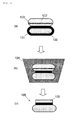
FIG. 1 is a flow chart of an embodiment of the inventive method for manufacturing an SOI wafer; and -
FIG. 2 is a flow chart of a conventional method for manufacturing an SOI wafer. - The present inventors considered how to inhibit an SOI island, which is an inherent defect that may occur when an SOI wafer is manufactured by the ion implantation separation method, and consequently conceived as follows. A region with a low bonding strength, which may be a cause of the occurrence of an SOI island, is eliminated by etching an insulator film interposed between a bond wafer and a base wafer to some extent from the outer circumferential edge toward the center before the bond wafer is separated; halfway transfer of an SOI layer can therefore be prevented in a region where the SOI island is easy to occur; in this region, the occurrence of the transfer of the SOI layer can reliably prevented, so the occurrence of the SOI island can be prevented.
- For this purpose, a bonded wafer needs to be immersed in an etching solution for an insulator film, such as hydrofluoric acid before the bond wafer is separated. As disclosed in JPH10-70054A, for example, it was previously understood that since it is feared that immersing a bonding interface in the state of a low bonging strength in an etching solution causes the etching solution to erode the bonding interface, a bonding heat treatment at a high temperature (for example, 1000°C or more) is needed before the immersion in an etching solution.
- When the ion implantation separation method is used, however, such a high-temperature heat treatment before etching causes the separation of the bond wafer at the layer of the implanted ions, so the SOI island cannot be consequently prevented. The present inventors accordingly investigated how far the etching of a silicon oxide film at the bonding interface proceeds when immersed in an etching solution after the bonding at room temperature, and consequently found that the etching at the bonding interface between a silicon oxide film and bare silicon proceeds only about 10 mm from the outer circumference, even when the oxide film is immersed in a 50% HF containing solution for one day (24 hours).
- On the other hand, it was found that when an insulator film is formed on the base wafer side and the above etching is performed according to Patent Document 2, an SOI wafer warps after separation. As shown in
FIG. 2 , when abond wafer 102 in which alayer 103 of implanted ions is formed and abase wafer 100 on which aninsulator film 101 is formed are bonded together (FIG. 2 at (a) ), and the resultant is immersed in anHF containing solution 104 to etch theinsulator film 101 at the bonding interface (FIG. 2 at (b) ), a part of the insulator film on the back surface of thebase wafer 100 is also removed, so after thebond wafer 102 is separated along thelayer 103 of implanted ions to form anSOI layer 105, anSOI wafer 106 in which the insulator film has been removed from the back surface of thebase wafer 100 is obtained (FIG. 2 at (c) ). - In this case, warping occurs due to a difference in thermal expansion coefficients between the insulator film and silicon as described above.
- The insulator film needs to remain on the back surface of the base wafer to inhibit this warping. The inventors considered how to prevent the occurrence of an SOI island on a terrace while inhibiting the occurrence of warping, and found that both the prevention of the occurrence of the SOI island and the inhibition of the warping can be achieved by etching a part of the insulator film between the bond wafer and the base wafer while protecting a part of the insulator film on the back surface of the base wafer before the bond wafer is separated; thereby the present invention has been completed.
- An embodiment of the present invention will now be described in detail with reference to figures, but the present invention is not limited to this embodiment.
-
FIG. 1 shows a flow chart of the inventive method for manufacturing an SOI wafer. - First, at least one type of gas ions selected from the group consisting of hydrogen ions and rare gas ions are implanted into a bond wafer composed of silicon single crystal from a surface of the bond wafer to form a layer of the implanted ions. Moreover, the insulator film is formed at least on all surfaces of a base wafer. In the present invention, the insulator film may be formed only on the base wafer. It is also permissible to form insulator films on both the base wafer and the bond wafer.
- The insulator film to be formed is not particularly limited, but typically an oxide film or a nitride film, or may also be a stacked layer film thereof.
- As shown in
FIG. 1 at (a) , the surface from which the ions are implanted into thebond wafer 10 having thelayer 11 of the implanted ions formed thereon and a surface of thebase wafer 12 are bonded through theinsulator film 13 at room temperature to form a bondedwafer 14. - A plasma treatment may also be performed on a surface to be bonded of at least one of the wafers before bonding to increase the bonding strength obtained at room temperature.
- After the above bonding process, it is preferable not to perform any heat treatment or to perform a heat treatment at a low temperature (for example, 200 to 350°C) that does not cause separation of the
bond wafer 10 at thelayer 11 of the implanted ions, before a subsequent etching process. - In this way, the separation of the bond wafer before etching, which is concerned when a conventional ion implantation separation method is used, can be prevented. In addition, the terrace width can more accurately be controlled.
- After that, as shown in
FIG. 1 at (b) , while apart 13b of the insulator film, which is on the back surface on the opposite side from the bonded surface of thebase wafer 12, is protected, the bondedwafer 14 is brought into contact with a liquid capable of dissolving the insulator film or exposed to a gas capable of dissolving the insulator film; a part 13a of the insulator film, which is interposed between thebond wafer 10 and thebase wafer 12, is thereby etched from the outer circumferential edge of the bondedwafer 14 and toward the center of the bonded wafer. - The etching may be performed by immersing the bonded wafer in an etching solution 15 (a liquid capable of dissolving the insulator film), as shown in
FIG. 1 at (b) , or exposing the bonded wafer to steam capable of dissolving the insulator film. - If the insulator film is an oxide film, then an HF containing solution is preferable as the
etching solution 15, but buffered hydrofluoric acid, an HF/H2O2/CH3COOH solution, and an HF/HNO3 solution may also be used. If the insulator film is a nitride film, then phosphoric acid is preferably used. - The
part 13b of the insulator film on the back surface of thebase wafer 12 can be protected by bringing the entire circumferential portion near the outer edge of the back surface of thebase wafer 12 into contact with a ring-shaped rubber 19 (an O-ring) to block the etching solution or the etching gas, as shown inFIG. 1 at (b) , or attaching a protective sheet, such as PVC, to thepart 13b of the insulator film on the back surface of thebase wafer 12. A possible alternative way is that the back surface of thebase wafer 12 is held by suction, and while the bondedwafer 14 is horizontally oriented and rotated, the etching solution or the etching gas is supplied from above thebond wafer 10 and a non-etching gas is supplied on the back surface side of thebase wafer 12, such that the etching solution or the etching gas does not reach the back surface of the base wafer because of wind pressure of the non-etching gas and centrifugal force generated by the rotation of the bondedwafer 14. - The insulator film at the bonding interface is eroded from its outer circumferential edge by this etching. At a portion where the insulator film has been eroded, the bond wafer and the base wafer are not bonded; when the bond wafer is separated, an SOI layer is not transferred at the eroded portion, so a terrace is formed thereon. At a region where the insulator film remains, on the other hand, the SOI layer is transferred by the separation. In other words, the width of the erosion due to the above etching equals the terrace width. In contrast, the part of the insulator film on the back surface of the base wafer is not etched because of the protection by the O-ring and so on.
- The SOI island occurs at a boundary portion between the SOI layer and the terrace. The boundary portion corresponds to an outer circumferential portion of a wafer to be bonded and has poor flatness, so this portion is a region where the SOI layer is only partially transferred because the portion has low bonding strength. The prevention of the occurrence of the SOI island needs to widen the erosion width of the insulator film by the above etching of the insulator film up to the region where the SOI island may occur and thereby to etch the above portion having low bonding strength; this prevents the transfer of the SOI layer at this region, thereby reliably eliminating the occurrence of the SOI island.
- The erosion width from the outer circumference of the insulator film by the above etching of the insulator film varies depending on the type of insulator film, and the type, concentration, and temperature of the etching solution or etching gas. Under the same conditions, however, since the erosion width can be controlled by etching time, the terrace width after the transfer of the SOI layer can also be controlled by adjustment of these conditions.
- The part 13a of the insulator film is preferably etched, for example, up to a location from 0.3 mm to 10 mm away from the outer circumferential edge of the bonded
wafer 14 and toward the center of the bonded wafer. - Adjustment of this erosion width enables the above region where the SOI island is easy to occur to be etched and removed, enabling the occurrence of the SOI island to be reliably prevented by adjustment of the terrace width. A chamfer portion with a width of about several hundred micrometers is typically formed on the outer circumferential edge of a
bond wafer 10 and abase wafer 12 that will form a bondedwafer 14. Since this chamfer portion is not bonded and does not form the SOI island thereon, the erosion width is more preferably 0.5 mm or more and, in view of an effective area of the SOI layer, more preferably 3 mm or less. - The range of protection of the back surface of the
base wafer 12 is not particularly limited; several millimeters from the outer circumference is desirable to inhibit the occurrence of warping of thebase wafer 12. Depending on a permissible level of warping, however, it may be protected within the inside of this range. A preferable protection range is, for example, within the inside of a location from 0 mm to 20 mm away from the outer circumferential edge of thebase wafer 12 and toward the center of the base wafer. This protection range can be adjusted, for example, by providing the O-ring 19 at a position from 0 mm to 20 mm away from the outer circumferential edge of thebase wafer 12 and toward the center of the base wafer. - The protected insulator film remaining in this range enables reliable inhibition of warping of a manufactured SOI wafer.
- As shown in
FIG. 1 at (c) , the bondedwafer 14 subjected to the etching of the insulator film 13a as above is then immersed in a liquid capable of dissolving silicon single crystal or exposed to a gas capable of dissolving silicon single crystal. The outercircumferential portion 18 of thebond wafer 10 is thereby etched up to a depth from the bonded surface of the bond wafer to at least thelayer 11 of the implanted ion. This etching is also preferable. - Such Si etching of the outer circumferential portion of the bond wafer enables a part that will become an extraneous particle in a device fabrication process to be previously removed. The occurrence of the SOI island is thereby prevented more reliably. In addition, since the layer of the implanted ions in the outer circumferential portion of the bond wafer is removed, blistering (a phenomenon of the occurrence of a swell) on the outer circumferential portion does not occur even when a heat treatment is performed in a subsequent process. Si swarf caused by the blistering can therefore be prevented from attaching to the terrace of the SOI wafer. It is to be noted that since attached Si swarf is not bonded to a base wafer unlike the SOI island, the swarf can be removed by general cleaning to some extent, but it is hard to completely remove the swarf. It is accordingly desirable to inhibit the attachment of Si swarf as possible by the above Si etching of the outer circumferential portion.
- Examples of the liquid capable of dissolving silicon single crystal include a tetramethyl ammonium hydroxide (TMAH) solution. This is not a limitation, provided a liquid or gas capable of dissolving silicon single crystal is used.
- Before this Si etching, an outer circumferential portion of the bond wafer and the base wafer that is outside a desired range in which the Si etching is performed is preferably protected in advance by a mask to prevent excessive etching thereof.
- As shown in
FIG. 1 at (d) , a separation heat treatment, for example, at 400°C or more is then performed to separate thebond wafer 10 along thelayer 11 of the implanted ions so that anSOI wafer 17 having anSOI layer 16 formed on the insulator film (buried insulator film) 13a is manufactured. - The present invention can control the terrace width, prevent the occurrence of an SOI island, inhibit increase in warping after separation, and thereby manufacture a high quality SOI wafer.
- The present invention will be now more specifically described with reference to Examples and Comparative Examples, but the present invention is not limited to these examples.
- In Example 1, a 300-mm-diameter silicon single crystal wafer (a bond wafer) and a 300-mm-diameter silicon single crystal wafer (a base wafer) in which a 150-nm-thickness thermal oxide film is formed on all surfaces were bonded at room temperature (25°C). After the bonding, while a part of the oxide film on the back surface of the base wafer was protected by an O-ring, an HF process (immersion in a 50% HF solution) was performed (the step at (b) in
FIG. 1 ). A separation heat treatment was then performed to separate the bond wafer so that an SOI wafer was manufactured. - In Example 2, an SOI wafer was manufactured as in Example 1 except that Si etching of the outer circumferential portion of the bond wafer by TMAH was added after the HF process (the step at (c) in
FIG. 1 ). - In Comparative Example 1, an SOI wafer was manufactured as in Example 1 except that after bonding, a separation heat treatment was performed to separate a bond wafer without performing the HF process.
- In Comparative Example 2, an SOI wafer was manufactured as in Example 1 except that after bonding, the HF process (immersion in a 50% HF solution) was performed without protecting the back surface of the base wafer (the step at (b) in
FIG. 2 ), and a separation heat treatment was then performed to separate the bond wafer. - Table 1 shows the conditions and evaluation results of Examples 1, 2 and Comparative Examples 1, 2.
(Table 1) EXAMPLE 1 EXAMPLE 2 COMPARATIVE EXAMPLE 1 COMPARATIVE EXAMPLE 2 THERMAL OXIDE FILM THICKNESS (BASE WAFER) Ox=150nm Ox=150nm Ox=150nm Ox=150nm ION IMPLANTATION CONDITION (BOND WAFER) 40keV, 6e16cm-2 40keV, 6e16cm-2 40keV, 6e16cm-2 40keV, 6e16cm-2 BONDING TEMPERATURE ROOM TEMPARATURE ROOM TEMPARATURE ROOM TEMPARATURE ROOM TEMPARATURE HF PROCESS 50%HF solution, 10min (*1) 50%HF solution, 60min (*2) NONE 50%HF solution, 10min (*3) Si ETCHING NONE (*4) NONE NONE SEPARATION HEAT TREATMENT, SEPARATION 500°C, 30min 500°C, 30min 500°C, 30min 500°C, 30min OXIDE FILM ON BACK SURFACE EXISTED EXISTED EXISTED NO EXISTED (REMOVED) WARP 10µm 10µm 10µm 40µm TERRACE OBSERVATION AFTER SEPARATION (OPTICAL MICROSCOPE) TERRACE WIDTH:1.1mm, NO SOI ISLAND EXISTED TERRACE WIDTH:1.1mm, NO SOI ISLAND EXISTED TERRACE WIDTH: 1.0 mm, SOI ISLAND EXISTED TERRACE WIDTH:1.1mm, NO SOI ISLAND EXISTED *1) The oxide film on the back surface was protected in the range between the wafer center and 3 mm away from the outer circumferential edge.
*2) The oxide film on the back surface was protected in the range between the wafer center and 5 mm away from the outer circumferential edge.
*3) There was no protection of the oxide film on the back surface.
*4) Si in the outer circumferential portion of the bond wafer was etched by 2 µm by a TMAH solution. - As shown in Table 1, the occurrence of an SOI island was able to be prevented by the etching in the present invention. In addition, warping was able to be inhibited by leaving the oxide film on the back surface of the base wafer. In Comparative Example 1 in which the HF process was not performed, on the other hand, the SOI island was detected. In Comparative Example 2 in which the HF process was performed without protecting the oxide film on the back surface of the base wafer, large warp occurred.
- It is to be noted that the present invention is not limited to the foregoing embodiment. The embodiment is just an exemplification, and any examples that have substantially the same feature and demonstrate the same functions and effects as those in the technical concept described in claims of the present invention are included in the technical scope of the present invention.
Claims (8)
- A method for manufacturing an SOI wafer, comprising:implanting at least one gas ion selected from a hydrogen ion and a rare gas ion into a bond wafer composed of silicon single crystal from a surface of the bond wafer to form a layer of the implanted ion;bonding the surface from which the ion is implanted into the bond wafer and a surface of a base wafer through an insulator film; and thenseparating the bond wafer along the layer of the implanted ion to form the SOI wafer, whereinthe insulator film is formed at least on all surfaces of the base wafer, and while protecting a first part of the insulator film, the first part being on a back surface on the opposite side from a bonded surface of the base wafer, a bonded wafer before separating the bond wafer along the layer of the implanted ion is brought into contact with a liquid capable of dissolving the insulator film or exposed to a gas capable of dissolving the insulator film, such that a second part of the insulator film is etched from an outer circumferential edge of the bonded wafer and toward the center of the bonded wafer, the second part being interposed between the bond wafer and the base wafer.
- The method for manufacturing an SOI wafer according to claim 1, wherein after bonding the bond wafer and the base wafer at room temperature, the insulator film is etched without heat treatment.
- The method for manufacturing an SOI wafer according to claim 1, wherein after bonding the bond wafer and the base wafer at room temperature, a heat treatment at a low temperature is performed such that the bond wafer is not separated along the layer of the implanted ion, and the insulator film is then etched.
- The method for manufacturing an SOI wafer according to any one of claims 1 to 3, wherein the second part of the insulator film is etched up to a location from 0.3 mm to 10 mm away from the outer circumferential edge of the bonded wafer and toward the center of the bonded wafer.
- The method for manufacturing an SOI wafer according to any one of claims 1 to 4, wherein during the etching of the insulator film, the first part of the insulator film on the back surface on the opposite side from the bonded surface of the base wafer is protected within the inside of a location from 0 mm to 20 mm away from the outer circumferential edge of the base wafer and toward the center of the base wafer.
- The method for manufacturing an SOI wafer according to any one of claims 1 to 5, wherein the first part of the insulator film on the back surface on the opposite side from the bonded surface of the base wafer is protected with an O-ring.
- The method for manufacturing an SOI wafer according to any one of claims 1 to 6, wherein the insulator film is any one of an oxide film, a nitride film, and a stacked layer film thereof, and the liquid capable of dissolving the insulator film is a solution containing hydrogen fluoride (HF).
- The method for manufacturing an SOI wafer according to any one of claims 1 to 7, wherein the bond wafer is separated, after the bonded wafer subjected to the etching of the insulator film is immersed into a liquid capable of dissolving single crystal silicon or exposed to a gas capable of dissolving single crystal silicon such that an outer circumferential portion of the bond wafer is etched up to a depth from the bonded surface of the bond wafer to at least the layer of the implanted ion.
Applications Claiming Priority (2)
| Application Number | Priority Date | Filing Date | Title |
|---|---|---|---|
| JP2012119066A JP5978764B2 (en) | 2012-05-24 | 2012-05-24 | Manufacturing method of SOI wafer |
| PCT/JP2013/002651 WO2013175705A1 (en) | 2012-05-24 | 2013-04-19 | Method for manufacturing soi wafer |
Publications (3)
| Publication Number | Publication Date |
|---|---|
| EP2858092A1 true EP2858092A1 (en) | 2015-04-08 |
| EP2858092A4 EP2858092A4 (en) | 2016-03-02 |
| EP2858092B1 EP2858092B1 (en) | 2019-10-09 |
Family
ID=49623420
Family Applications (1)
| Application Number | Title | Priority Date | Filing Date |
|---|---|---|---|
| EP13794721.4A Active EP2858092B1 (en) | 2012-05-24 | 2013-04-19 | Method for manufacturing soi wafer |
Country Status (8)
| Country | Link |
|---|---|
| US (1) | US9029240B2 (en) |
| EP (1) | EP2858092B1 (en) |
| JP (1) | JP5978764B2 (en) |
| KR (1) | KR101914755B1 (en) |
| CN (1) | CN104364880B (en) |
| SG (1) | SG11201406680PA (en) |
| TW (1) | TWI594323B (en) |
| WO (1) | WO2013175705A1 (en) |
Families Citing this family (3)
| Publication number | Priority date | Publication date | Assignee | Title |
|---|---|---|---|---|
| KR102067713B1 (en) * | 2016-05-31 | 2020-01-17 | 주식회사 엘지화학 | Battery module, battery pack comprising the battery module and vehicle comprising the battery pack |
| US20180019169A1 (en) * | 2016-07-12 | 2018-01-18 | QMAT, Inc. | Backing substrate stabilizing donor substrate for implant or reclamation |
| FR3076393A1 (en) * | 2017-12-28 | 2019-07-05 | Commissariat A L'energie Atomique Et Aux Energies Alternatives | METHOD OF TRANSFERRING A USEFUL LAYER |
Family Cites Families (15)
| Publication number | Priority date | Publication date | Assignee | Title |
|---|---|---|---|---|
| US5405518A (en) * | 1994-04-26 | 1995-04-11 | Industrial Technology Research Institute | Workpiece holder apparatus |
| JPH08107091A (en) * | 1994-09-30 | 1996-04-23 | Kyushu Komatsu Denshi Kk | Manufacture of soi substrate |
| US5668045A (en) * | 1994-11-30 | 1997-09-16 | Sibond, L.L.C. | Process for stripping outer edge of BESOI wafers |
| US5494849A (en) * | 1995-03-23 | 1996-02-27 | Si Bond L.L.C. | Single-etch stop process for the manufacture of silicon-on-insulator substrates |
| US5937312A (en) * | 1995-03-23 | 1999-08-10 | Sibond L.L.C. | Single-etch stop process for the manufacture of silicon-on-insulator wafers |
| JPH1116861A (en) * | 1997-06-20 | 1999-01-22 | Toshiba Corp | Production of semiconductor device |
| JP4304879B2 (en) | 2001-04-06 | 2009-07-29 | 信越半導体株式会社 | Method for determining the implantation amount of hydrogen ions or rare gas ions |
| KR100577627B1 (en) * | 2002-05-20 | 2006-05-10 | 주식회사 사무코 | Bonding substrate, its manufacturing method and jig for wafer outer peripheral pressurization |
| JP2004022838A (en) * | 2002-06-17 | 2004-01-22 | Sumitomo Mitsubishi Silicon Corp | Laminated soi substrate and method for manufacturing the same |
| FR2880184B1 (en) * | 2004-12-28 | 2007-03-30 | Commissariat Energie Atomique | METHOD OF SORTING A STRUCTURE OBTAINED BY ASSEMBLING TWO PLATES |
| JP2006216662A (en) | 2005-02-02 | 2006-08-17 | Sumco Corp | Process for producing bonding soi wafer, and the bonding soi wafer |
| JP4398934B2 (en) | 2005-02-28 | 2010-01-13 | 信越半導体株式会社 | Manufacturing method of SOI wafer |
| JP5194508B2 (en) | 2007-03-26 | 2013-05-08 | 信越半導体株式会社 | Manufacturing method of SOI wafer |
| JP5244650B2 (en) * | 2009-02-26 | 2013-07-24 | 信越半導体株式会社 | Manufacturing method of SOI wafer |
| JP2011071193A (en) * | 2009-09-24 | 2011-04-07 | Sumco Corp | Lamination soi wafer and manufacturing method of the same |
-
2012
- 2012-05-24 JP JP2012119066A patent/JP5978764B2/en active Active
-
2013
- 2013-04-19 US US14/394,598 patent/US9029240B2/en active Active
- 2013-04-19 CN CN201380026585.8A patent/CN104364880B/en active Active
- 2013-04-19 WO PCT/JP2013/002651 patent/WO2013175705A1/en not_active Ceased
- 2013-04-19 KR KR1020147031656A patent/KR101914755B1/en active Active
- 2013-04-19 EP EP13794721.4A patent/EP2858092B1/en active Active
- 2013-04-19 SG SG11201406680PA patent/SG11201406680PA/en unknown
- 2013-05-03 TW TW102115892A patent/TWI594323B/en active
Also Published As
| Publication number | Publication date |
|---|---|
| KR20150013164A (en) | 2015-02-04 |
| JP2013247204A (en) | 2013-12-09 |
| TW201401369A (en) | 2014-01-01 |
| US9029240B2 (en) | 2015-05-12 |
| WO2013175705A1 (en) | 2013-11-28 |
| KR101914755B1 (en) | 2018-11-05 |
| EP2858092B1 (en) | 2019-10-09 |
| CN104364880B (en) | 2017-09-26 |
| EP2858092A4 (en) | 2016-03-02 |
| CN104364880A (en) | 2015-02-18 |
| SG11201406680PA (en) | 2014-12-30 |
| TWI594323B (en) | 2017-08-01 |
| JP5978764B2 (en) | 2016-08-24 |
| US20150064875A1 (en) | 2015-03-05 |
Similar Documents
| Publication | Publication Date | Title |
|---|---|---|
| EP2402983B1 (en) | Method for manufacturing soi wafer | |
| KR101901872B1 (en) | Soi wafer manufacturing method | |
| EP2924736B1 (en) | Method for manufacturing soi wafer | |
| JP6380245B2 (en) | Manufacturing method of SOI wafer | |
| EP2858092B1 (en) | Method for manufacturing soi wafer | |
| KR102019658B1 (en) | Soi wafer manufacturing method | |
| US6878630B2 (en) | Method of manufacturing a wafer | |
| KR102095383B1 (en) | Method for manufacturing bonded wafer | |
| JP2010153488A (en) | Manufacturing method of soi wafer, and soi wafer | |
| EP3029730B1 (en) | Bonded wafer manufacturing method | |
| KR20160052551A (en) | Bonded wafer manufacturing method | |
| JP2010040540A (en) | Method of manufacturing simox substrate |
Legal Events
| Date | Code | Title | Description |
|---|---|---|---|
| PUAI | Public reference made under article 153(3) epc to a published international application that has entered the european phase |
Free format text: ORIGINAL CODE: 0009012 |
|
| 17P | Request for examination filed |
Effective date: 20141021 |
|
| AK | Designated contracting states |
Kind code of ref document: A1 Designated state(s): AL AT BE BG CH CY CZ DE DK EE ES FI FR GB GR HR HU IE IS IT LI LT LU LV MC MK MT NL NO PL PT RO RS SE SI SK SM TR |
|
| AX | Request for extension of the european patent |
Extension state: BA ME |
|
| DAX | Request for extension of the european patent (deleted) | ||
| RAP1 | Party data changed (applicant data changed or rights of an application transferred) |
Owner name: SHIN-ETSU HANDOTAI CO., LTD. |
|
| RA4 | Supplementary search report drawn up and despatched (corrected) |
Effective date: 20160128 |
|
| RIC1 | Information provided on ipc code assigned before grant |
Ipc: H01L 27/12 20060101ALI20160122BHEP Ipc: H01L 21/265 20060101ALI20160122BHEP Ipc: H01L 21/02 20060101AFI20160122BHEP Ipc: H01L 21/308 20060101ALI20160122BHEP Ipc: H01L 21/20 20060101ALI20160122BHEP Ipc: H01L 21/306 20060101ALI20160122BHEP Ipc: H01L 21/322 20060101ALI20160122BHEP Ipc: H01L 21/762 20060101ALI20160122BHEP |
|
| STAA | Information on the status of an ep patent application or granted ep patent |
Free format text: STATUS: EXAMINATION IS IN PROGRESS |
|
| 17Q | First examination report despatched |
Effective date: 20181025 |
|
| GRAP | Despatch of communication of intention to grant a patent |
Free format text: ORIGINAL CODE: EPIDOSNIGR1 |
|
| STAA | Information on the status of an ep patent application or granted ep patent |
Free format text: STATUS: GRANT OF PATENT IS INTENDED |
|
| INTG | Intention to grant announced |
Effective date: 20190516 |
|
| GRAS | Grant fee paid |
Free format text: ORIGINAL CODE: EPIDOSNIGR3 |
|
| GRAA | (expected) grant |
Free format text: ORIGINAL CODE: 0009210 |
|
| STAA | Information on the status of an ep patent application or granted ep patent |
Free format text: STATUS: THE PATENT HAS BEEN GRANTED |
|
| AK | Designated contracting states |
Kind code of ref document: B1 Designated state(s): AL AT BE BG CH CY CZ DE DK EE ES FI FR GB GR HR HU IE IS IT LI LT LU LV MC MK MT NL NO PL PT RO RS SE SI SK SM TR |
|
| REG | Reference to a national code |
Ref country code: GB Ref legal event code: FG4D |
|
| REG | Reference to a national code |
Ref country code: CH Ref legal event code: EP |
|
| REG | Reference to a national code |
Ref country code: DE Ref legal event code: R096 Ref document number: 602013061522 Country of ref document: DE |
|
| REG | Reference to a national code |
Ref country code: IE Ref legal event code: FG4D |
|
| REG | Reference to a national code |
Ref country code: AT Ref legal event code: REF Ref document number: 1189796 Country of ref document: AT Kind code of ref document: T Effective date: 20191115 |
|
| REG | Reference to a national code |
Ref country code: NL Ref legal event code: MP Effective date: 20191009 |
|
| REG | Reference to a national code |
Ref country code: LT Ref legal event code: MG4D |
|
| REG | Reference to a national code |
Ref country code: AT Ref legal event code: MK05 Ref document number: 1189796 Country of ref document: AT Kind code of ref document: T Effective date: 20191009 |
|
| PG25 | Lapsed in a contracting state [announced via postgrant information from national office to epo] |
Ref country code: PT Free format text: LAPSE BECAUSE OF FAILURE TO SUBMIT A TRANSLATION OF THE DESCRIPTION OR TO PAY THE FEE WITHIN THE PRESCRIBED TIME-LIMIT Effective date: 20200210 Ref country code: GR Free format text: LAPSE BECAUSE OF FAILURE TO SUBMIT A TRANSLATION OF THE DESCRIPTION OR TO PAY THE FEE WITHIN THE PRESCRIBED TIME-LIMIT Effective date: 20200110 Ref country code: ES Free format text: LAPSE BECAUSE OF FAILURE TO SUBMIT A TRANSLATION OF THE DESCRIPTION OR TO PAY THE FEE WITHIN THE PRESCRIBED TIME-LIMIT Effective date: 20191009 Ref country code: AT Free format text: LAPSE BECAUSE OF FAILURE TO SUBMIT A TRANSLATION OF THE DESCRIPTION OR TO PAY THE FEE WITHIN THE PRESCRIBED TIME-LIMIT Effective date: 20191009 Ref country code: NL Free format text: LAPSE BECAUSE OF FAILURE TO SUBMIT A TRANSLATION OF THE DESCRIPTION OR TO PAY THE FEE WITHIN THE PRESCRIBED TIME-LIMIT Effective date: 20191009 Ref country code: BG Free format text: LAPSE BECAUSE OF FAILURE TO SUBMIT A TRANSLATION OF THE DESCRIPTION OR TO PAY THE FEE WITHIN THE PRESCRIBED TIME-LIMIT Effective date: 20200109 Ref country code: FI Free format text: LAPSE BECAUSE OF FAILURE TO SUBMIT A TRANSLATION OF THE DESCRIPTION OR TO PAY THE FEE WITHIN THE PRESCRIBED TIME-LIMIT Effective date: 20191009 Ref country code: NO Free format text: LAPSE BECAUSE OF FAILURE TO SUBMIT A TRANSLATION OF THE DESCRIPTION OR TO PAY THE FEE WITHIN THE PRESCRIBED TIME-LIMIT Effective date: 20200109 Ref country code: LT Free format text: LAPSE BECAUSE OF FAILURE TO SUBMIT A TRANSLATION OF THE DESCRIPTION OR TO PAY THE FEE WITHIN THE PRESCRIBED TIME-LIMIT Effective date: 20191009 Ref country code: PL Free format text: LAPSE BECAUSE OF FAILURE TO SUBMIT A TRANSLATION OF THE DESCRIPTION OR TO PAY THE FEE WITHIN THE PRESCRIBED TIME-LIMIT Effective date: 20191009 Ref country code: LV Free format text: LAPSE BECAUSE OF FAILURE TO SUBMIT A TRANSLATION OF THE DESCRIPTION OR TO PAY THE FEE WITHIN THE PRESCRIBED TIME-LIMIT Effective date: 20191009 Ref country code: SE Free format text: LAPSE BECAUSE OF FAILURE TO SUBMIT A TRANSLATION OF THE DESCRIPTION OR TO PAY THE FEE WITHIN THE PRESCRIBED TIME-LIMIT Effective date: 20191009 |
|
| PG25 | Lapsed in a contracting state [announced via postgrant information from national office to epo] |
Ref country code: HR Free format text: LAPSE BECAUSE OF FAILURE TO SUBMIT A TRANSLATION OF THE DESCRIPTION OR TO PAY THE FEE WITHIN THE PRESCRIBED TIME-LIMIT Effective date: 20191009 Ref country code: RS Free format text: LAPSE BECAUSE OF FAILURE TO SUBMIT A TRANSLATION OF THE DESCRIPTION OR TO PAY THE FEE WITHIN THE PRESCRIBED TIME-LIMIT Effective date: 20191009 Ref country code: IS Free format text: LAPSE BECAUSE OF FAILURE TO SUBMIT A TRANSLATION OF THE DESCRIPTION OR TO PAY THE FEE WITHIN THE PRESCRIBED TIME-LIMIT Effective date: 20200224 |
|
| PG25 | Lapsed in a contracting state [announced via postgrant information from national office to epo] |
Ref country code: AL Free format text: LAPSE BECAUSE OF FAILURE TO SUBMIT A TRANSLATION OF THE DESCRIPTION OR TO PAY THE FEE WITHIN THE PRESCRIBED TIME-LIMIT Effective date: 20191009 |
|
| REG | Reference to a national code |
Ref country code: DE Ref legal event code: R097 Ref document number: 602013061522 Country of ref document: DE |
|
| PG2D | Information on lapse in contracting state deleted |
Ref country code: IS |
|
| PG25 | Lapsed in a contracting state [announced via postgrant information from national office to epo] |
Ref country code: RO Free format text: LAPSE BECAUSE OF FAILURE TO SUBMIT A TRANSLATION OF THE DESCRIPTION OR TO PAY THE FEE WITHIN THE PRESCRIBED TIME-LIMIT Effective date: 20191009 Ref country code: CZ Free format text: LAPSE BECAUSE OF FAILURE TO SUBMIT A TRANSLATION OF THE DESCRIPTION OR TO PAY THE FEE WITHIN THE PRESCRIBED TIME-LIMIT Effective date: 20191009 Ref country code: DK Free format text: LAPSE BECAUSE OF FAILURE TO SUBMIT A TRANSLATION OF THE DESCRIPTION OR TO PAY THE FEE WITHIN THE PRESCRIBED TIME-LIMIT Effective date: 20191009 Ref country code: EE Free format text: LAPSE BECAUSE OF FAILURE TO SUBMIT A TRANSLATION OF THE DESCRIPTION OR TO PAY THE FEE WITHIN THE PRESCRIBED TIME-LIMIT Effective date: 20191009 Ref country code: IS Free format text: LAPSE BECAUSE OF FAILURE TO SUBMIT A TRANSLATION OF THE DESCRIPTION OR TO PAY THE FEE WITHIN THE PRESCRIBED TIME-LIMIT Effective date: 20200209 |
|
| PLBE | No opposition filed within time limit |
Free format text: ORIGINAL CODE: 0009261 |
|
| STAA | Information on the status of an ep patent application or granted ep patent |
Free format text: STATUS: NO OPPOSITION FILED WITHIN TIME LIMIT |
|
| PG25 | Lapsed in a contracting state [announced via postgrant information from national office to epo] |
Ref country code: SK Free format text: LAPSE BECAUSE OF FAILURE TO SUBMIT A TRANSLATION OF THE DESCRIPTION OR TO PAY THE FEE WITHIN THE PRESCRIBED TIME-LIMIT Effective date: 20191009 Ref country code: SM Free format text: LAPSE BECAUSE OF FAILURE TO SUBMIT A TRANSLATION OF THE DESCRIPTION OR TO PAY THE FEE WITHIN THE PRESCRIBED TIME-LIMIT Effective date: 20191009 Ref country code: IT Free format text: LAPSE BECAUSE OF FAILURE TO SUBMIT A TRANSLATION OF THE DESCRIPTION OR TO PAY THE FEE WITHIN THE PRESCRIBED TIME-LIMIT Effective date: 20191009 |
|
| 26N | No opposition filed |
Effective date: 20200710 |
|
| PG25 | Lapsed in a contracting state [announced via postgrant information from national office to epo] |
Ref country code: SI Free format text: LAPSE BECAUSE OF FAILURE TO SUBMIT A TRANSLATION OF THE DESCRIPTION OR TO PAY THE FEE WITHIN THE PRESCRIBED TIME-LIMIT Effective date: 20191009 Ref country code: MC Free format text: LAPSE BECAUSE OF FAILURE TO SUBMIT A TRANSLATION OF THE DESCRIPTION OR TO PAY THE FEE WITHIN THE PRESCRIBED TIME-LIMIT Effective date: 20191009 |
|
| REG | Reference to a national code |
Ref country code: CH Ref legal event code: PL |
|
| PG25 | Lapsed in a contracting state [announced via postgrant information from national office to epo] |
Ref country code: LI Free format text: LAPSE BECAUSE OF NON-PAYMENT OF DUE FEES Effective date: 20200430 Ref country code: LU Free format text: LAPSE BECAUSE OF NON-PAYMENT OF DUE FEES Effective date: 20200419 Ref country code: CH Free format text: LAPSE BECAUSE OF NON-PAYMENT OF DUE FEES Effective date: 20200430 |
|
| REG | Reference to a national code |
Ref country code: BE Ref legal event code: MM Effective date: 20200430 |
|
| PG25 | Lapsed in a contracting state [announced via postgrant information from national office to epo] |
Ref country code: BE Free format text: LAPSE BECAUSE OF NON-PAYMENT OF DUE FEES Effective date: 20200430 |
|
| GBPC | Gb: european patent ceased through non-payment of renewal fee |
Effective date: 20200419 |
|
| PG25 | Lapsed in a contracting state [announced via postgrant information from national office to epo] |
Ref country code: IE Free format text: LAPSE BECAUSE OF NON-PAYMENT OF DUE FEES Effective date: 20200419 Ref country code: GB Free format text: LAPSE BECAUSE OF NON-PAYMENT OF DUE FEES Effective date: 20200419 |
|
| PG25 | Lapsed in a contracting state [announced via postgrant information from national office to epo] |
Ref country code: TR Free format text: LAPSE BECAUSE OF FAILURE TO SUBMIT A TRANSLATION OF THE DESCRIPTION OR TO PAY THE FEE WITHIN THE PRESCRIBED TIME-LIMIT Effective date: 20191009 Ref country code: MT Free format text: LAPSE BECAUSE OF FAILURE TO SUBMIT A TRANSLATION OF THE DESCRIPTION OR TO PAY THE FEE WITHIN THE PRESCRIBED TIME-LIMIT Effective date: 20191009 Ref country code: CY Free format text: LAPSE BECAUSE OF FAILURE TO SUBMIT A TRANSLATION OF THE DESCRIPTION OR TO PAY THE FEE WITHIN THE PRESCRIBED TIME-LIMIT Effective date: 20191009 |
|
| PG25 | Lapsed in a contracting state [announced via postgrant information from national office to epo] |
Ref country code: MK Free format text: LAPSE BECAUSE OF FAILURE TO SUBMIT A TRANSLATION OF THE DESCRIPTION OR TO PAY THE FEE WITHIN THE PRESCRIBED TIME-LIMIT Effective date: 20191009 |
|
| PGFP | Annual fee paid to national office [announced via postgrant information from national office to epo] |
Ref country code: DE Payment date: 20250422 Year of fee payment: 13 |
|
| PGFP | Annual fee paid to national office [announced via postgrant information from national office to epo] |
Ref country code: FR Payment date: 20250425 Year of fee payment: 13 |
|
| REG | Reference to a national code |
Ref country code: DE Ref legal event code: R079 Ref document number: 602013061522 Country of ref document: DE Free format text: PREVIOUS MAIN CLASS: H01L0021020000 Ipc: H10P0095000000 |