EP2857892A2 - Backlight module - Google Patents
Backlight module Download PDFInfo
- Publication number
- EP2857892A2 EP2857892A2 EP20140200614 EP14200614A EP2857892A2 EP 2857892 A2 EP2857892 A2 EP 2857892A2 EP 20140200614 EP20140200614 EP 20140200614 EP 14200614 A EP14200614 A EP 14200614A EP 2857892 A2 EP2857892 A2 EP 2857892A2
- Authority
- EP
- European Patent Office
- Prior art keywords
- parts
- reflecting
- peripheral
- frame
- reflecting member
- Prior art date
- Legal status (The legal status is an assumption and is not a legal conclusion. Google has not performed a legal analysis and makes no representation as to the accuracy of the status listed.)
- Granted
Links
Images


Classifications
-
- G—PHYSICS
- G02—OPTICS
- G02F—OPTICAL DEVICES OR ARRANGEMENTS FOR THE CONTROL OF LIGHT BY MODIFICATION OF THE OPTICAL PROPERTIES OF THE MEDIA OF THE ELEMENTS INVOLVED THEREIN; NON-LINEAR OPTICS; FREQUENCY-CHANGING OF LIGHT; OPTICAL LOGIC ELEMENTS; OPTICAL ANALOGUE/DIGITAL CONVERTERS
- G02F1/00—Devices or arrangements for the control of the intensity, colour, phase, polarisation or direction of light arriving from an independent light source, e.g. switching, gating or modulating; Non-linear optics
- G02F1/01—Devices or arrangements for the control of the intensity, colour, phase, polarisation or direction of light arriving from an independent light source, e.g. switching, gating or modulating; Non-linear optics for the control of the intensity, phase, polarisation or colour
- G02F1/13—Devices or arrangements for the control of the intensity, colour, phase, polarisation or direction of light arriving from an independent light source, e.g. switching, gating or modulating; Non-linear optics for the control of the intensity, phase, polarisation or colour based on liquid crystals, e.g. single liquid crystal display cells
- G02F1/133—Constructional arrangements; Operation of liquid crystal cells; Circuit arrangements
- G02F1/1333—Constructional arrangements; Manufacturing methods
- G02F1/1335—Structural association of cells with optical devices, e.g. polarisers or reflectors
- G02F1/1336—Illuminating devices
- G02F1/133602—Direct backlight
- G02F1/133605—Direct backlight including specially adapted reflectors
-
- F—MECHANICAL ENGINEERING; LIGHTING; HEATING; WEAPONS; BLASTING
- F21—LIGHTING
- F21V—FUNCTIONAL FEATURES OR DETAILS OF LIGHTING DEVICES OR SYSTEMS THEREOF; STRUCTURAL COMBINATIONS OF LIGHTING DEVICES WITH OTHER ARTICLES, NOT OTHERWISE PROVIDED FOR
- F21V7/00—Reflectors for light sources
- F21V7/04—Optical design
-
- G—PHYSICS
- G02—OPTICS
- G02F—OPTICAL DEVICES OR ARRANGEMENTS FOR THE CONTROL OF LIGHT BY MODIFICATION OF THE OPTICAL PROPERTIES OF THE MEDIA OF THE ELEMENTS INVOLVED THEREIN; NON-LINEAR OPTICS; FREQUENCY-CHANGING OF LIGHT; OPTICAL LOGIC ELEMENTS; OPTICAL ANALOGUE/DIGITAL CONVERTERS
- G02F1/00—Devices or arrangements for the control of the intensity, colour, phase, polarisation or direction of light arriving from an independent light source, e.g. switching, gating or modulating; Non-linear optics
- G02F1/01—Devices or arrangements for the control of the intensity, colour, phase, polarisation or direction of light arriving from an independent light source, e.g. switching, gating or modulating; Non-linear optics for the control of the intensity, phase, polarisation or colour
- G02F1/13—Devices or arrangements for the control of the intensity, colour, phase, polarisation or direction of light arriving from an independent light source, e.g. switching, gating or modulating; Non-linear optics for the control of the intensity, phase, polarisation or colour based on liquid crystals, e.g. single liquid crystal display cells
- G02F1/133—Constructional arrangements; Operation of liquid crystal cells; Circuit arrangements
- G02F1/1333—Constructional arrangements; Manufacturing methods
- G02F1/1335—Structural association of cells with optical devices, e.g. polarisers or reflectors
- G02F1/1336—Illuminating devices
- G02F1/133602—Direct backlight
- G02F1/133608—Direct backlight including particular frames or supporting means
Definitions
- the present invention generally relates to a backlight module.
- a conventional liquid crystal module includes a liquid crystal cell and a backlight device.
- the backlight device is disposed directly behind the liquid crystal cell.
- the backlight device mainly includes a linear light source, a light reflecting member, a plurality of optical sheets and a frame.
- the linear light source includes a straight tube or U-tube fluorescent tube. Electrodes at the ends of the linear light source are fitted into a power socket.
- the light reflecting member is disposed at the back of the linear light source.
- the light reflecting member includes a reflecting face. The light from the linear light source is reflected by the light reflecting member, and shines from the back onto the liquid crystal cell.
- the optical sheets include a light diffusing plate, and are disposed in the required type and number between the light reflecting member and the liquid crystal cell.
- the frame supports the linear light source, the light reflecting member and the optical sheets.
- the frame is made of molded resin or sheet metal.
- the linear light source and the light reflecting member are mounted in the frame. All or substantially all of the surface of the light reflecting member is a reflecting face.
- the reflecting face is divided into one wide, rectangular center region located at the back of the linear light source, and slender, trapezoidal peripheral regions that are raised up in a slanted orientation from four sides of the center region.
- the light reflecting member is formed by combining a sheet that can be bent, and frame pieces.
- the frame pieces are formed from resin by injection molding.
- the sheet is bent along straight bending lines set at places near the two long sides, and has a silhouette shape that is substantially rectangular.
- the sheet is bent and held so that the rectangular center region and two of the trapezoidal peripheral regions on either side of the center region are formed in the sheet.
- the ends in the lengthwise direction of each of the peripheral regions are formed in a shape such that the spacing between the ends of each of the peripheral regions widens moving away from the bending lines.
- the peripheral regions are formed in a trapezoidal shape.
- the frame piece is a resin molding formed by injection molding.
- the frame piece has a slender, slanted, trapezoidal reflecting face.
- the frame pieces are disposed symmetrically on either side in the lengthwise direction of the sheet.
- the slender, trapezoidal reflecting faces of the frame pieces are used as the other two peripheral regions.
- the ends of the slender, trapezoidal reflecting faces of the frame pieces are butted against the ends of the slender, trapezoidal peripheral regions formed by the sheet, and the butting configuration of the four peripheral regions forms a rectangular shape.
- the light from a light source is reflected by a reflecting plate (see Japanese Laid-Open Patent Application Nos. 2004-102119 and 2004-55182 , for example).
- a reflecting plate see Japanese Laid-Open Patent Application Nos. 2004-102119 and 2004-55182 , for example.
- uneven brightness is avoided by providing a peaked portion to the reflecting plate.
- warping of the reflecting plate is prevented by using a multilayer structure for the reflecting plate.
- the light reflecting member is a combination of the sheet with the two frame pieces
- three components are required to form the light reflecting member, namely, the sheet and the two frame pieces. This not only increases the cost, but also makes the assembly process more complicated and diminishes productivity.
- the present invention is conceived in light of the above-mentioned problems.
- One object of the present invention is to provide a backlight device whose production cost is reduced.
- a backlight module includes at least one light source, a light reflecting member, and a frame.
- the at least one light source is configured to emit light.
- the light reflecting member is arranged to reflect the light emitted from the light source.
- the light reflecting member includes a center reflecting part, two first peripheral reflecting parts, two second peripheral reflecting parts, and two extension parts.
- the center reflecting part has two first opposite side portions and two second opposite side portions.
- the first peripheral reflecting parts each have a first trapezoidal shape with a first lower base and a first upper base that is longer than the first lower base.
- the first lower bases are connected to the first opposite side portions of the center reflecting part, respectively, such that the first peripheral reflecting parts extend from the first opposite side portions of the center reflecting part, respectively.
- the second peripheral reflecting parts each have a second trapezoidal shape with a second lower base and a second upper base that is longer than the second lower base.
- the second lower bases are connected to the second opposite side portions of the center reflecting part, respectively, such that the second peripheral reflecting parts extend from the second opposite side portions of the center reflecting part, respectively.
- the extension parts extend from either the first upper bases or the second upper bases, respectively.
- the center reflecting part, the first peripheral reflecting parts, the second peripheral reflecting parts and the extension parts are integrally formed as a one-piece, unitary member.
- the frame includes a bottom part, two first side parts and two second side parts. The first and second side parts extend frontward from peripheral portions of the bottom part with respect to the bottom part, respectively. The first and second side parts define an interior of the frame therebetween.
- the light reflecting member is arranged with respect to the frame while the light reflecting member is attached to the frame such that the center reflecting part, the first peripheral reflecting parts and the second peripheral reflecting parts are disposed within the interior of the frame, and such that the extension parts are disposed on either the first side parts or the second side parts, respectively.
- a backlight device for a liquid crystal module includes a linear light source and a light reflecting member.
- the linear light source is configured to emit light.
- the light reflecting member is arranged to reflect the light emitted from the linear light source toward a liquid crystal cell of the liquid crystal module.
- the light reflecting member includes a center reflecting face, a pair of first peripheral reflecting faces and a pair of second peripheral reflecting faces.
- the center reflecting face is formed in a rectangular shape and disposed rearward with respect to the linear light source.
- the pair of first peripheral reflecting faces is formed in a trapezoidal shape and extends from a pair of first opposing side portions of the center reflecting face frontward and outward with respect to the center reflecting face, respectively.
- the pair of second peripheral reflecting faces is formed in a trapezoidal shape and extends from a pair of second opposing side portions of the center reflecting face frontward and outward with respect to the center reflecting face, respectively.
- the center reflecting face and the first and second peripheral reflecting faces are integrally formed from a sheet-like member as a one-piece, unitary member.
- the backlight device of the present invention it is possible to provide a back light device whose production cost is reduced.
- the light reflecting member further includes a bent portion that is disposed between the center reflecting face and each of the first and second peripheral reflecting faces and extends along each of the first and second opposing side portions of the center reflecting face.
- an end portion of one of the first peripheral reflecting faces abuts an end portion of one of the second peripheral reflecting faces that is adjacent to the one of the first peripheral reflecting faces to form a corner section of the light reflecting member at a corner portion of the center reflecting face with the corner portion of the center reflecting face being located between the one of the first peripheral reflecting faces and the one of the second peripheral reflecting faces.
- the light reflecting member further includes a coupling portion that couples the end portion of the first peripheral reflecting face with the end portion of the second peripheral reflecting face.
- the coupling portion includes an insertion tab that extends from one of the end portion of the first peripheral reflecting face and the end portion of the second peripheral reflecting face, and an slit portion that is formed on the other of the end portion of the first peripheral reflecting face and the end portion of the second peripheral reflecting face, the insertion tab being disposed through the slit portion to couple the end portion of the first peripheral reflecting face with the end portion of the second peripheral reflecting face.
- the first opposing side portions are longer than the second opposing side portions in length, and at least one of the second peripheral reflecting faces further includes a through hole with a continuous periphery, a part of the linear light source being disposed through the through hole of the second peripheral reflecting face.
- a liquid crystal module includes a liquid crystal cell (not shown) and a backlight device.
- the backlight device is disposed directly behind the liquid crystal cell.
- the backlight device mainly includes a pair of linear light sources 1, a light reflecting member 3, a plurality of optical sheets 4 and a frame 5.
- the linear light sources 1 emit light.
- Each of the linear light sources 1 includes a U-shaped fluorescent tube.
- the linear light source 1 has electrodes at ends of the linear light source 1. The electrodes are inserted into power sockets 2 to supply electronic power to the linear light source 1.
- the light reflecting member 3 is disposed at the back (e.g., the rear side) of the linear light source 1, and has a reflecting face.
- the light from the linear light source 1 is reflected by the light reflecting member 3, and shines from the back toward the liquid crystal cell.
- the light reflecting member 3 is formed as a one-piece, unitary member.
- the optical sheets 4 includes a light diffusing plate, and are disposed in the required type and number between the light reflecting member 3 and the liquid crystal cell. The light reflected by the reflecting face of the light reflecting member 3 passes through the optical sheets 4, and shines on the liquid crystal cell from the back. As a result, the brightness balance of a display face of the liquid crystal cell is maintained.
- the linear light source 1, the light reflecting member 3 and the optical sheets 4 are supported on the frame 5.
- the frame 5 is made of molded resin or sheet metal.
- the light reflecting member 3 is made of a sheet (e.g., sheet-like member) 8.
- the entire light reflecting member 3 is formed by just the single sheet 8 as a one-piece, unitary member.
- the light reflecting member 3 is not formed by combining a sheet with frame pieces, as the conventional light reflecting member. All or substantially all of the surface of the light reflecting member 3 is a reflecting face.
- the sheet 8 has a center region (e.g., center reflecting face) Z1, a pair of top and bottom peripheral regions (e.g., a pair of first peripheral reflecting faces) Z2 and Z4, and a pair of left and right trapezoidal peripheral regions (e.g., a pair of second peripheral reflecting faces) Z3 and Z5.
- the center region Z1 is formed in a rectangular shape.
- the center region Z1 is located at the back of the linear light source 1.
- the peripheral regions Z2, Z3, Z4, and Z5 are formed in a trapezoidal shape.
- the peripheral regions Z2, Z3, Z4, and Z5 are raised up in a slanted orientation from four sides 11, 12, 13, and 14 of the center region Z1.
- the top and bottom peripheral regions Z2 and Z4 extend from top and bottom long side portions (e.g., a pair of first opposing side portions) of the center region Z1 frontward and outward with respect to the center region Z1.
- the left and right peripheral regions Z3 and Z5 extend from left and right short side portions (e.g., a pair of second opposing side portions) of the center region Z1 frontward and outward with respect to the center region Z1.
- the sheet 8 is bent at four places around the periphery of the center region Z1 along straight bending lines (e.g., bent portions) L11, L12, L13, and L14, which forms the peripheral regions Z2, Z3, Z4, and Z5, and also forms the center region Z1 having the four sides 11, 12, 13, and 14 that are formed by the bending lines L11, L12, L13, and L14. Therefore, the center region Z1 has a wide, rectangular region bounded by the four sides 11, 12, 13, and 14. Also, the peripheral regions Z2, Z3, Z4, and Z5 has slender, trapezoidal regions that are raised up in the slanted orientation from the four sides 11, 12, 13, and 14 of the center region Z1, respectively.
- straight bending lines e.g., bent portions
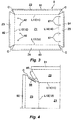
- the sheet 8 When the sheet 8 is spread out as shown in FIG. 3 , the sheet 8 has a shape in which V-shaped cuts C having the same shape are formed at four corners of a rectangular sheet material.
- the straight lines that connect the bottom points (e.g., the vertex) of the cuts C correspond to the bending lines L11, L12, L13, and L14.
- the rectangular region bounded by the bending lines L11, L12, L13, and L14 corresponds to the center region Z1. Therefore, the places where the bending lines L11, L12, L13, and L14 are formed correspond to the four sides 11, 12, 13, and 14 of the center region Z1.
- Outer regions of the four bending lines L11, L12, L13, and L14 are trapezoidal in shape.
- the trapezoidal regions correspond to the peripheral regions Z2, Z3, Z4, and Z5.
- slender extension tabs 81, 82, 83, and 84 are provided to outer edges of the peripheral regions Z2, Z3, Z4, and Z5, respectively.
- the extension tabs 81, 82, 83, and 84 are narrow in width.
- the ends (e.g., end portions) of the peripheral regions Z2, Z3, Z4, and Z5 are butted together to form butt joints (e.g., corner sections) a so that there is no gap in between.
- the extension tabs 81, 82, 83, and 84 of the outer edges of the peripheral regions Z2, Z3, Z4, and Z5 are bent outward.
- the extension tabs 81, 82, 83, and 84 correspond to the portions supported by the frame 5 as shown in FIG. 1 .
- the U-shaped fluorescent tubes are used for the linear light source 1.
- the end electrodes of the linear light source 1 are connected to the power sockets 2 disposed in the empty space at the back of the peripheral region Z5 of the sheet 8.
- the linear light source 1 passes through holes 87 formed in the peripheral region Z5 and sticks out to the rear of the peripheral region Z5, where it is connected to the power sockets 2.
- Each of the through holes 87 has a closed hole with a continuous periphery.
- a fixing piece 9 is affixed to the frame 5.
- the fixing piece 9 has clamps 91.
- the clamps 91 stick out to the front side of the sheet 8 from openings 92 made at places on the center region Z1 of the sheet 8.
- the clamps 91 support the linear light sources 1 at suitable locations, such as the two locations of the bent portion shown in FIG. 5 .
- the light reflecting member 3 is formed by just a single sheet 8, and furthermore the sheet 8 is formed by bending a substantially rectangular sheet material with the shape shown in FIG. 3 at an angle and at four places around the periphery of the material.
- the cost of producing the light reflecting member 3 is markedly lower than the conventional light reflecting member.
- the assembly process for the light reflecting member 3 involves merely bending a single sheet material at four places around its periphery and at an angle.
- the process is much simpler than the conventional light reflecting member that requires skill to combine the sheet with the frame pieces. Therefore, this promotes a simpler assembly process for the backlight device, and the productivity tends to be higher.
- the reflecting faces are formed on the light reflecting member 3.
- the center region Z1 located at the back of the linear light source 1 and the peripheral regions Z2, Z3, Z4, and Z5 that are raised up in a slanted orientation from the four sides 11 to 14 of the center region Z1 are all formed by just the one sheet 8. Accordingly, there is no need to form the center region Z1 and the peripheral regions Z2, Z3, Z4, and Z5 by combining the conventional sheet with the conventional frame pieces.
- the light reflecting member 3 can be formed by just the one sheet 8. As a result, there is no need to using extra components such as the frame pieces, and the number of parts that are needed can be correspondingly reduced. This promotes a simpler assembly process.
- the sheet 8 is more readily available and much less expensive than a resin molding formed by injection molding, which is expensive and demands sophisticated technology, as with the conventional frame pieces. Therefore, with the backlight device, it is possible to provide a backlight device much more inexpensively. Furthermore, this helps reduce the weight of the backlight device.
- the linear light sources 1 include the U-shaped fluorescent tubes, and the bent portions of the linear light sources 1 are supported by the clamps 91 at locations between the peripheral regions Z3 and Z5.
- the bent portions of the linear light sources 1 can be positioned on the back side of the peripheral region Z3, and be supported by clamps formed on the frame 5 at locations back side of the peripheral region Z3.
- the peripheral region Z3 also has through holes through which the linear light sources 1 are disposed.
- the linear light sources 1 can include a plurality of (four in FIG. 6 ) straight tubes.
- the peripheral region Z3 has two pairs of through holes 88 through which the left end portions of the linear light sources 1 are disposed
- the peripheral region Z5 has two pairs of through holes 87 through which the right end portions of the linear light sources 1 are disposed.
- FIG. 4 a backlight device in accordance with a second embodiment will now be explained.
- the parts of the second embodiment that are identical to the parts of the first embodiment will be given the same reference numerals as the parts of the first embodiment.
- the descriptions of the parts of the second embodiment that are identical to the parts of the first embodiment may be omitted for the sake of brevity.
- the parts of the second embodiment that differ from the parts of the first embodiment will be indicated with a double prime (").
- FIG. 4 is a detail development view of the sheet 8" in accordance with the second embodiment.
- the sheet 8" has a coupling portion that couples the top and bottom peripheral regions Z2 and Z4 with the left and right peripheral regions Z3 and Z5, respectively.
- the coupling portion includes four insertion tabs 85 and four slits 86.
- the insertion tabs 85 are provided to and extend from horizontal end portions of the peripheral regions Z2 and Z4.
- the slits 86 are formed at vertical end portions of the peripheral regions Z3 and Z5.
- Each of the insertion tabs 85 is inserted into the corresponding one of the slits 86.
- the insertion tab 85 is provided to the end of one peripheral region (such as the peripheral region Z2 in FIG.
- the slit 86 is formed at the end of the other peripheral region (such as the peripheral region Z3 in FIG. 4 ).
- the insertion tab 85 is inserted into the slit 86, and latched to the slit 86 to couple the one peripheral region with the other peripheral region.
- the insertion tab 85 can also be formed at the end of one peripheral region out of any one of the adjacent pairs of the peripheral regions (e.g., the peripheral regions Z3 and Z4, the peripheral regions Z4 and Z5, the peripheral regions Z5 and Z2, etc.) that are adjacent to one another and flank one of the corners of the center region Z1, and the slit 86 can be formed in the other peripheral region.
- the peripheral regions Z3 and Z4, the peripheral regions Z4 and Z5, the peripheral regions Z5 and Z2, etc. can be formed in the other peripheral region.
- the sheet 8" With the sheet 8", the sheet 8" can be held in the shape shown in FIG. 2 by bending at an angle along the bending lines L11, L12, L13, and L14.
- the insertion tabs 85 on the one peripheral regions are inserted into the insertion slits 86 on the other peripheral regions from either inside or outside of the one peripheral regions.
- the adjacent pairs of the peripheral regions (the peripheral regions Z2 and Z3, the peripheral regions Z3 and Z4, the peripheral regions Z4 and Z5, and the peripheral regions Z5 and Z2) are linked at the places where the insertion tabs 85 are inserted into the slits 86. Accordingly, this improves the ability of the sheet 8" to maintain the shape shown in FIG. 2 .
- the stability of light reflection by the sheet 8" is increased. Furthermore, it becomes less likely that the brightness of the liquid crystal cell is uneven.
Landscapes
- Physics & Mathematics (AREA)
- Nonlinear Science (AREA)
- Mathematical Physics (AREA)
- Chemical & Material Sciences (AREA)
- Crystallography & Structural Chemistry (AREA)
- General Physics & Mathematics (AREA)
- Optics & Photonics (AREA)
- Engineering & Computer Science (AREA)
- General Engineering & Computer Science (AREA)
- Planar Illumination Modules (AREA)
- Liquid Crystal (AREA)
Abstract
Description
- This application claims priority to Japanese Patent Application No.
2008-211261, filed on August 20 2008 2008-211261 - The present invention generally relates to a backlight module.
- A conventional liquid crystal module includes a liquid crystal cell and a backlight device. The backlight device is disposed directly behind the liquid crystal cell.
- The backlight device mainly includes a linear light source, a light reflecting member, a plurality of optical sheets and a frame. The linear light source includes a straight tube or U-tube fluorescent tube. Electrodes at the ends of the linear light source are fitted into a power socket. The light reflecting member is disposed at the back of the linear light source. The light reflecting member includes a reflecting face. The light from the linear light source is reflected by the light reflecting member, and shines from the back onto the liquid crystal cell. The optical sheets include a light diffusing plate, and are disposed in the required type and number between the light reflecting member and the liquid crystal cell. The light reflected by the reflecting face of the light reflecting member passes through the optical sheets, and shines on the liquid crystal cell from the back, which maintains the brightness balance of an image display face of the liquid crystal cell. The frame supports the linear light source, the light reflecting member and the optical sheets. The frame is made of molded resin or sheet metal.
- The linear light source and the light reflecting member are mounted in the frame. All or substantially all of the surface of the light reflecting member is a reflecting face. The reflecting face is divided into one wide, rectangular center region located at the back of the linear light source, and slender, trapezoidal peripheral regions that are raised up in a slanted orientation from four sides of the center region.
- With the conventional backlight device, the light reflecting member is formed by combining a sheet that can be bent, and frame pieces. The frame pieces are formed from resin by injection molding.
- The sheet is bent along straight bending lines set at places near the two long sides, and has a silhouette shape that is substantially rectangular. The sheet is bent and held so that the rectangular center region and two of the trapezoidal peripheral regions on either side of the center region are formed in the sheet. In the two peripheral regions formed by the sheet, the ends in the lengthwise direction of each of the peripheral regions are formed in a shape such that the spacing between the ends of each of the peripheral regions widens moving away from the bending lines. Thus, the peripheral regions are formed in a trapezoidal shape.
- The frame piece is a resin molding formed by injection molding. The frame piece has a slender, slanted, trapezoidal reflecting face. The frame pieces are disposed symmetrically on either side in the lengthwise direction of the sheet. The slender, trapezoidal reflecting faces of the frame pieces are used as the other two peripheral regions. The ends of the slender, trapezoidal reflecting faces of the frame pieces are butted against the ends of the slender, trapezoidal peripheral regions formed by the sheet, and the butting configuration of the four peripheral regions forms a rectangular shape.
- Meanwhile, with another conventional backlight device, the light from a light source is reflected by a reflecting plate (see Japanese Laid-Open Patent Application Nos.
2004-102119 2004-55182 - However, when the light reflecting member is a combination of the sheet with the two frame pieces, three components are required to form the light reflecting member, namely, the sheet and the two frame pieces. This not only increases the cost, but also makes the assembly process more complicated and diminishes productivity.
- In view of the above, it will be apparent to those skilled in the art from this disclosure that there exists a need for an improved backlight device. This invention addresses this need in the art as well as other needs, which will become apparent to those skilled in the art from this disclosure.
- The present invention is conceived in light of the above-mentioned problems. One object of the present invention is to provide a backlight device whose production cost is reduced.
- In accordance with one aspect of the present disclosure, a backlight module includes at least one light source, a light reflecting member, and a frame. The at least one light source is configured to emit light. The light reflecting member is arranged to reflect the light emitted from the light source. The light reflecting member includes a center reflecting part, two first peripheral reflecting parts, two second peripheral reflecting parts, and two extension parts. The center reflecting part has two first opposite side portions and two second opposite side portions. The first peripheral reflecting parts each have a first trapezoidal shape with a first lower base and a first upper base that is longer than the first lower base. The first lower bases are connected to the first opposite side portions of the center reflecting part, respectively, such that the first peripheral reflecting parts extend from the first opposite side portions of the center reflecting part, respectively. The second peripheral reflecting parts each have a second trapezoidal shape with a second lower base and a second upper base that is longer than the second lower base. The second lower bases are connected to the second opposite side portions of the center reflecting part, respectively, such that the second peripheral reflecting parts extend from the second opposite side portions of the center reflecting part, respectively. The extension parts extend from either the first upper bases or the second upper bases, respectively. The center reflecting part, the first peripheral reflecting parts, the second peripheral reflecting parts and the extension parts are integrally formed as a one-piece, unitary member. The frame includes a bottom part, two first side parts and two second side parts. The first and second side parts extend frontward from peripheral portions of the bottom part with respect to the bottom part, respectively. The first and second side parts define an interior of the frame therebetween. The light reflecting member is arranged with respect to the frame while the light reflecting member is attached to the frame such that the center reflecting part, the first peripheral reflecting parts and the second peripheral reflecting parts are disposed within the interior of the frame, and such that the extension parts are disposed on either the first side parts or the second side parts, respectively.
- These and other objects, features, aspects and advantages of the present invention will become apparent to those skilled in the art from the following detailed descriptions, which, taken in conjunction with the annexed drawings, disclose selected embodiments of the present invention.
- Referring now to the attached drawings which form a part of this original disclosure:
-
FIG. 1 is a cross sectional view of a backlight device for a liquid crystal module in accordance with a first embodiment of the present invention; -
FIG. 2 is a perspective view of a light reflecting member of the backlight device illustrated inFIG. 1 ; -
FIG. 3 is a development view of the light reflecting member illustrated inFIG. 2 ; -
FIG. 4 is a detail development view of a light reflecting member in accordance with a second embodiment of the present invention; -
FIG. 5 is a front elevational view of the backlight device illustrated inFIG. 1 ; and -
FIG. 6 is a front elevational view of another example of the backlight device. - Selected embodiments of the present invention will now be explained with reference to the drawings. It will be apparent to those skilled in the art from these disclosures that the following descriptions of the selected embodiments of the present invention are provided for illustration only and not for the purpose of limiting the invention as defined by the appended claims and their equivalents.
- In accordance with a first aspect of the present invention, a backlight device for a liquid crystal module includes a linear light source and a light reflecting member. The linear light source is configured to emit light. The light reflecting member is arranged to reflect the light emitted from the linear light source toward a liquid crystal cell of the liquid crystal module. The light reflecting member includes a center reflecting face, a pair of first peripheral reflecting faces and a pair of second peripheral reflecting faces. The center reflecting face is formed in a rectangular shape and disposed rearward with respect to the linear light source. The pair of first peripheral reflecting faces is formed in a trapezoidal shape and extends from a pair of first opposing side portions of the center reflecting face frontward and outward with respect to the center reflecting face, respectively. The pair of second peripheral reflecting faces is formed in a trapezoidal shape and extends from a pair of second opposing side portions of the center reflecting face frontward and outward with respect to the center reflecting face, respectively. The center reflecting face and the first and second peripheral reflecting faces are integrally formed from a sheet-like member as a one-piece, unitary member.
- With the backlight device of the present invention, it is possible to provide a back light device whose production cost is reduced.
- In accordance with a second aspect of the present invention, with the backlight device according to the first aspect of the present invention, the light reflecting member further includes a bent portion that is disposed between the center reflecting face and each of the first and second peripheral reflecting faces and extends along each of the first and second opposing side portions of the center reflecting face.
- In accordance with a third aspect of the present invention, with the backlight device according to the first aspect of the present invention, an end portion of one of the first peripheral reflecting faces abuts an end portion of one of the second peripheral reflecting faces that is adjacent to the one of the first peripheral reflecting faces to form a corner section of the light reflecting member at a corner portion of the center reflecting face with the corner portion of the center reflecting face being located between the one of the first peripheral reflecting faces and the one of the second peripheral reflecting faces.
- In accordance with a fourth aspect of the present invention, with the backlight device according to the third aspect of the present invention, the light reflecting member further includes a coupling portion that couples the end portion of the first peripheral reflecting face with the end portion of the second peripheral reflecting face.
- In accordance with a fifth aspect of the present invention, with the backlight device according to the fourth aspect of the present invention, the coupling portion includes an insertion tab that extends from one of the end portion of the first peripheral reflecting face and the end portion of the second peripheral reflecting face, and an slit portion that is formed on the other of the end portion of the first peripheral reflecting face and the end portion of the second peripheral reflecting face, the insertion tab being disposed through the slit portion to couple the end portion of the first peripheral reflecting face with the end portion of the second peripheral reflecting face.
- In accordance with a sixth aspect of the present invention, with the backlight device according to the fifth aspect of the present invention, the first opposing side portions are longer than the second opposing side portions in length, and at least one of the second peripheral reflecting faces further includes a through hole with a continuous periphery, a part of the linear light source being disposed through the through hole of the second peripheral reflecting face.
- A liquid crystal module includes a liquid crystal cell (not shown) and a backlight device. The backlight device is disposed directly behind the liquid crystal cell. As shown in
FIGS. 1 and5 , the backlight device mainly includes a pair of linearlight sources 1, alight reflecting member 3, a plurality ofoptical sheets 4 and aframe 5. The linearlight sources 1 emit light. Each of the linearlight sources 1 includes a U-shaped fluorescent tube. The linearlight source 1 has electrodes at ends of the linearlight source 1. The electrodes are inserted into power sockets 2 to supply electronic power to the linearlight source 1. Thelight reflecting member 3 is disposed at the back (e.g., the rear side) of the linearlight source 1, and has a reflecting face. The light from the linearlight source 1 is reflected by thelight reflecting member 3, and shines from the back toward the liquid crystal cell. Thelight reflecting member 3 is formed as a one-piece, unitary member. Theoptical sheets 4 includes a light diffusing plate, and are disposed in the required type and number between thelight reflecting member 3 and the liquid crystal cell. The light reflected by the reflecting face of thelight reflecting member 3 passes through theoptical sheets 4, and shines on the liquid crystal cell from the back. As a result, the brightness balance of a display face of the liquid crystal cell is maintained. The linearlight source 1, thelight reflecting member 3 and theoptical sheets 4 are supported on theframe 5. Theframe 5 is made of molded resin or sheet metal. - As shown in
FIG. 2 , thelight reflecting member 3 is made of a sheet (e.g., sheet-like member) 8. The entirelight reflecting member 3 is formed by just thesingle sheet 8 as a one-piece, unitary member. In other words, thelight reflecting member 3 is not formed by combining a sheet with frame pieces, as the conventional light reflecting member. All or substantially all of the surface of thelight reflecting member 3 is a reflecting face. - The
sheet 8 has a center region (e.g., center reflecting face) Z1, a pair of top and bottom peripheral regions (e.g., a pair of first peripheral reflecting faces) Z2 and Z4, and a pair of left and right trapezoidal peripheral regions (e.g., a pair of second peripheral reflecting faces) Z3 and Z5. The center region Z1 is formed in a rectangular shape. The center region Z1 is located at the back of the linearlight source 1. The peripheral regions Z2, Z3, Z4, and Z5 are formed in a trapezoidal shape. The peripheral regions Z2, Z3, Z4, and Z5 are raised up in a slanted orientation from foursides sheet 8 is bent at four places around the periphery of the center region Z1 along straight bending lines (e.g., bent portions) L11, L12, L13, and L14, which forms the peripheral regions Z2, Z3, Z4, and Z5, and also forms the center region Z1 having the foursides sides sides - When the
sheet 8 is spread out as shown inFIG. 3 , thesheet 8 has a shape in which V-shaped cuts C having the same shape are formed at four corners of a rectangular sheet material. The straight lines that connect the bottom points (e.g., the vertex) of the cuts C correspond to the bending lines L11, L12, L13, and L14. The rectangular region bounded by the bending lines L11, L12, L13, and L14 corresponds to the center region Z1. Therefore, the places where the bending lines L11, L12, L13, and L14 are formed correspond to the foursides - Outer regions of the four bending lines L11, L12, L13, and L14 are trapezoidal in shape. The trapezoidal regions correspond to the peripheral regions Z2, Z3, Z4, and Z5. With the
sheet 8,slender extension tabs extension tabs - When the trapezoidal regions are bent in the slanted orientation along the four straight bending lines L11, L12, L13, and L14, and the
sheet 8 is held in the shape shown inFIG. 2 , this forms the center region Z1 and the peripheral regions Z2, Z3, Z4, and Z5 that are raised up in the slanted orientation from the foursides extension tabs extension tabs frame 5 as shown inFIG. 1 . - As shown in
FIG. 5 , the U-shaped fluorescent tubes are used for the linearlight source 1. The end electrodes of the linearlight source 1 are connected to the power sockets 2 disposed in the empty space at the back of the peripheral region Z5 of thesheet 8. The linearlight source 1 passes throughholes 87 formed in the peripheral region Z5 and sticks out to the rear of the peripheral region Z5, where it is connected to the power sockets 2. Each of the throughholes 87 has a closed hole with a continuous periphery. On the back side of thesheet 8, a fixingpiece 9 is affixed to theframe 5. The fixingpiece 9 hasclamps 91. Theclamps 91 stick out to the front side of thesheet 8 fromopenings 92 made at places on the center region Z1 of thesheet 8. Theclamps 91 support the linearlight sources 1 at suitable locations, such as the two locations of the bent portion shown inFIG. 5 . - With the backlight device, the
light reflecting member 3 is formed by just asingle sheet 8, and furthermore thesheet 8 is formed by bending a substantially rectangular sheet material with the shape shown inFIG. 3 at an angle and at four places around the periphery of the material. Thus, the cost of producing thelight reflecting member 3 is markedly lower than the conventional light reflecting member. Also, the assembly process for thelight reflecting member 3 involves merely bending a single sheet material at four places around its periphery and at an angle. Thus, the process is much simpler than the conventional light reflecting member that requires skill to combine the sheet with the frame pieces. Therefore, this promotes a simpler assembly process for the backlight device, and the productivity tends to be higher. Furthermore, no gaps are produced at the boundary between each one of the adjacent pairs of the peripheral regions Z2, Z3, Z4, and Z5 (e.g., at the butt joints a). As a result, the light is appropriately reflected, and it is unlikely that the brightness of the liquid crystal cell is uneven. - With the backlight device, the reflecting faces are formed on the
light reflecting member 3. Specifically, the center region Z1 located at the back of the linearlight source 1 and the peripheral regions Z2, Z3, Z4, and Z5 that are raised up in a slanted orientation from the foursides 11 to 14 of the center region Z1, are all formed by just the onesheet 8. Accordingly, there is no need to form the center region Z1 and the peripheral regions Z2, Z3, Z4, and Z5 by combining the conventional sheet with the conventional frame pieces. Thus, thelight reflecting member 3 can be formed by just the onesheet 8. As a result, there is no need to using extra components such as the frame pieces, and the number of parts that are needed can be correspondingly reduced. This promotes a simpler assembly process. Furthermore, thesheet 8 is more readily available and much less expensive than a resin molding formed by injection molding, which is expensive and demands sophisticated technology, as with the conventional frame pieces. Therefore, with the backlight device, it is possible to provide a backlight device much more inexpensively. Furthermore, this helps reduce the weight of the backlight device. - As shown in
FIG. 5 , the linearlight sources 1 include the U-shaped fluorescent tubes, and the bent portions of the linearlight sources 1 are supported by theclamps 91 at locations between the peripheral regions Z3 and Z5. However, the bent portions of the linearlight sources 1 can be positioned on the back side of the peripheral region Z3, and be supported by clamps formed on theframe 5 at locations back side of the peripheral region Z3. In this case, the peripheral region Z3 also has through holes through which the linearlight sources 1 are disposed. Furthermore, as shown inFIG. 6 , the linearlight sources 1 can include a plurality of (four inFIG. 6 ) straight tubes. In this case, the peripheral region Z3 has two pairs of throughholes 88 through which the left end portions of the linearlight sources 1 are disposed, and the peripheral region Z5 has two pairs of throughholes 87 through which the right end portions of the linearlight sources 1 are disposed. - Referring now to
FIG. 4 , a backlight device in accordance with a second embodiment will now be explained. In view of the similarity between the first and second embodiments, the parts of the second embodiment that are identical to the parts of the first embodiment will be given the same reference numerals as the parts of the first embodiment. Moreover, the descriptions of the parts of the second embodiment that are identical to the parts of the first embodiment may be omitted for the sake of brevity. The parts of the second embodiment that differ from the parts of the first embodiment will be indicated with a double prime ("). -
FIG. 4 is a detail development view of thesheet 8" in accordance with the second embodiment. Thesheet 8" has a coupling portion that couples the top and bottom peripheral regions Z2 and Z4 with the left and right peripheral regions Z3 and Z5, respectively. The coupling portion includes fourinsertion tabs 85 and fourslits 86. Theinsertion tabs 85 are provided to and extend from horizontal end portions of the peripheral regions Z2 and Z4. Theslits 86 are formed at vertical end portions of the peripheral regions Z3 and Z5. Each of theinsertion tabs 85 is inserted into the corresponding one of theslits 86. For example, theinsertion tab 85 is provided to the end of one peripheral region (such as the peripheral region Z2 inFIG. 4 ) out of any one of the adjacent pairs of the peripheral regions (such as the peripheral regions Z2 and Z3 inFIG. 4 ) that are adjacent to one another and flank one of the corners of the center region Z1. Theslit 86 is formed at the end of the other peripheral region (such as the peripheral region Z3 inFIG. 4 ). Theinsertion tab 85 is inserted into theslit 86, and latched to theslit 86 to couple the one peripheral region with the other peripheral region. Theinsertion tab 85 can also be formed at the end of one peripheral region out of any one of the adjacent pairs of the peripheral regions (e.g., the peripheral regions Z3 and Z4, the peripheral regions Z4 and Z5, the peripheral regions Z5 and Z2, etc.) that are adjacent to one another and flank one of the corners of the center region Z1, and theslit 86 can be formed in the other peripheral region. - With the
sheet 8", thesheet 8" can be held in the shape shown inFIG. 2 by bending at an angle along the bending lines L11, L12, L13, and L14. Theinsertion tabs 85 on the one peripheral regions are inserted into the insertion slits 86 on the other peripheral regions from either inside or outside of the one peripheral regions. When theinsertion tabs 85 are thus inserted into theslits 86, the adjacent pairs of the peripheral regions (the peripheral regions Z2 and Z3, the peripheral regions Z3 and Z4, the peripheral regions Z4 and Z5, and the peripheral regions Z5 and Z2) are linked at the places where theinsertion tabs 85 are inserted into theslits 86. Accordingly, this improves the ability of thesheet 8" to maintain the shape shown inFIG. 2 . As a result, the stability of light reflection by thesheet 8" is increased. Furthermore, it becomes less likely that the brightness of the liquid crystal cell is uneven. - In understanding the scope of the present invention, the term "comprising" and its derivatives, as used herein, are intended to be open ended terms that specify the presence of the stated features, elements, components and groups, but do not exclude the presence of other unstated features, elements, components and groups. The foregoing also applies to words having similar meanings such as the terms, "including", "having" and their derivatives. Also, the terms "part," "section," "portion," "member" or "element" when used in the singular can have the dual meaning of a single part or a plurality of parts. As used herein to describe the present invention, the following directional terms "forward, rearward, above, downward, vertical, horizontal, below and transverse" as well as any other similar directional terms refer to those directions of a liquid crystal module equipped with the present invention. Accordingly, these terms, as utilized to describe the present invention should be interpreted relative to a liquid crystal module equipped with the present invention as used in the normal operating position.
- While selected embodiments have been chosen to illustrate the present invention, it will be apparent to those skilled in the art from these disclosures that various changes and modifications can be made herein without departing from the scope of the invention as defined in the appended claims. Furthermore, the foregoing descriptions of the selected embodiments according to the present invention are provided for illustration only, and not for the purpose of limiting the invention as defined by the appended claims and their equivalents.
Claims (16)
- A backlight module comprising:at least one light source configured to emit light;a light reflecting member arranged to reflect the light emitted from the light source, the light reflecting member including
a center reflecting part having two first opposite side portions and two second opposite side portions,
two first peripheral reflecting parts each having a first trapezoidal shape with a first lower base and a first upper base that is longer than the first lower base, the first lower bases being connected to the first opposite side portions of the center reflecting part, respectively, such that the first peripheral reflecting parts extend from the first opposite side portions of the center reflecting part, respectively,
two second peripheral reflecting parts each having a second trapezoidal shape with a second lower base and a second upper base that is longer than the second lower base, the second lower bases being connected to the second opposite side portions of the center reflecting part, respectively, such that the second peripheral reflecting parts extend from the second opposite side portions of the center reflecting part, respectively, and
two extension parts extending from either the first upper bases or the second upper bases, respectively, with the center reflecting part, the first peripheral reflecting parts, the second peripheral reflecting parts and the extension parts being integrally formed as a one-piece, unitary member; anda frame including a bottom part, two first side parts and two second side parts, the first and second side parts extending frontward from peripheral portions of the bottom part, respectively, the first and second side parts defining an interior of the frame therebetween,the light reflecting member being arranged with respect to the frame while the light reflecting member is attached to the frame such that the center reflecting part, the first peripheral reflecting parts and the second peripheral reflecting parts are disposed within the interior of the frame, and such that the extension parts are disposed on either the first side parts or the second side parts, respectively. - The backlight module according to claim 1, wherein
the extension parts of the light reflecting member are arranged parallel to the center reflecting part of the light reflecting member while the light reflecting member is attached to the frame. - The backlight module according to claim 1, further comprising
a plurality of optical sheets disposed on the light reflecting member such that the optical sheets at least partially overlap with the extension parts of the light reflecting member as viewed in a direction perpendicular to the center reflecting part while the light reflecting member is attached to the frame. - The backlight module according to claim 1, wherein
the light reflecting member further includes two additional extension parts extending from either the first upper bases or the second upper bases, from which the extension parts do not extend, respectively, and
the light reflecting member is further arranged with respect to the frame while the light reflecting member is attached to the frame such that the additional extension parts of the light reflecting member are disposed on either the first side parts or the second side parts, on which the extension parts are not disposed, respectively. - The backlight module according to claim 1, wherein
the extension parts of the light reflecting member are disposed along entire lengths of either the first upper bases or the second upper bases, respectively. - The backlight module according to claim 5, wherein
the extension parts of the light reflecting member have a rectangular shape. - The backlight module according to claim 5, wherein
the extension parts have a first width measured in a widthwise direction perpendicular to a lengthwise direction of the extension parts, and
either the first side parts or the second side parts on which the extension parts are disposed have a second width measured in the widthwise direction, with the second width being larger than the first width. - The backlight module according to claim 1, wherein
side end portions of an adjacent pair of the first peripheral reflecting parts and the second peripheral reflecting parts abut against each other to form a corner section of the light reflecting member at a corner portion of the center reflecting part while the light reflecting member is attached to the frame. - The backlight module according to claim 8, wherein
the light reflecting member further includes a tongue part that extends from one of the side end portions of the adjacent pair of the first peripheral reflecting parts and the second peripheral reflecting parts towards the other of the side end portions of the adjacent pair of the first peripheral reflecting parts and the second peripheral reflecting parts, and
the tongue part of the light reflecting member at least partially overlaps with the other of the side end portions of the adjacent pair of the first peripheral reflecting parts and the second peripheral reflecting parts while the light reflecting member is attached to the frame. - The backlight module according to claim 9, wherein
the tongue part of the light reflecting member has a distal edge extending between first and second ends of the tongue part, with the first end of the tongue part being located closer to the corner portion of the center reflecting part than the second end of the tongue part,
a distance between the distal edge of the tongue part and the other of the side end portions of the adjacent pair of the first peripheral reflecting parts and the second peripheral reflecting parts increases as approaching the second end of the tongue part from the first end of the tongue part along the distal edge of the tongue part. - The backlight module according to claim 10, wherein
the distal edge of the tongue part of the light reflecting member is disposed on a rear side of the other of the side end portions of the adjacent pair of the first peripheral reflecting parts and the second peripheral reflecting parts while the light reflecting member is attached to the frame. - The backlight module according to claim 11, wherein
each of the side end portions of the adjacent pair of the first peripheral reflecting parts and the second peripheral reflecting parts has first and second ends, with the first end of each of the side end portions being located closer to the corner portion of the center reflecting part than the second end of each of the side end portions, and
the tongue part is entirely disposed within an area enclosed by the side end portions and an imaginary line extending between the second ends of the side end portions. - The backlight module according to claim 1, wherein
one of the first and second side parts of the frame extends perpendicularly frontward with respect to the bottom part such that the one of the first and second side parts of the frame and corresponding one of the first and second peripheral reflecting parts that is adjacently opposite the one of the first and second side parts of the frame define a spacing therebetween while the light reflecting member is attached to the frame. - The backlight module according to claim 1, wherein
at least one of the first and second side parts of the frame has an outer surface that is perpendicular to the bottom part of the frame. - The backlight module according to claim 1, wherein
the first opposite side portions of the center reflecting part are longer than the second opposite side portions of the center reflecting part, respectively. - The backlight module according to claim 15, further comprising
a plurality of light sources arranged with respect to the frame, the light sources being connected to a plurality of electric connectors, respectively, the electric connectors being arranged closer to one of the second side parts of the frame than the other of the second side parts of the frame.
Applications Claiming Priority (2)
| Application Number | Priority Date | Filing Date | Title |
|---|---|---|---|
| JP2008211261A JP2010049846A (en) | 2008-08-20 | 2008-08-20 | Direct backlight device of liquid crystal module |
| EP09161741.5A EP2157474B1 (en) | 2008-08-20 | 2009-06-03 | Backlight device for liquid crystal module |
Related Parent Applications (2)
| Application Number | Title | Priority Date | Filing Date |
|---|---|---|---|
| EP09161741.5A Division EP2157474B1 (en) | 2008-08-20 | 2009-06-03 | Backlight device for liquid crystal module |
| EP09161741.5A Division-Into EP2157474B1 (en) | 2008-08-20 | 2009-06-03 | Backlight device for liquid crystal module |
Publications (3)
| Publication Number | Publication Date |
|---|---|
| EP2857892A2 true EP2857892A2 (en) | 2015-04-08 |
| EP2857892A3 EP2857892A3 (en) | 2015-06-24 |
| EP2857892B1 EP2857892B1 (en) | 2018-04-04 |
Family
ID=40957703
Family Applications (3)
| Application Number | Title | Priority Date | Filing Date |
|---|---|---|---|
| EP18205027.8A Active EP3460564B1 (en) | 2008-08-20 | 2009-06-03 | Backlight module |
| EP09161741.5A Active EP2157474B1 (en) | 2008-08-20 | 2009-06-03 | Backlight device for liquid crystal module |
| EP14200614.7A Active EP2857892B1 (en) | 2008-08-20 | 2009-06-03 | Backlight module |
Family Applications Before (2)
| Application Number | Title | Priority Date | Filing Date |
|---|---|---|---|
| EP18205027.8A Active EP3460564B1 (en) | 2008-08-20 | 2009-06-03 | Backlight module |
| EP09161741.5A Active EP2157474B1 (en) | 2008-08-20 | 2009-06-03 | Backlight device for liquid crystal module |
Country Status (3)
| Country | Link |
|---|---|
| US (5) | US8622565B2 (en) |
| EP (3) | EP3460564B1 (en) |
| JP (1) | JP2010049846A (en) |
Cited By (3)
| Publication number | Priority date | Publication date | Assignee | Title |
|---|---|---|---|---|
| CN105738992A (en) * | 2016-03-01 | 2016-07-06 | 达运精密工业股份有限公司 | Reflector plate |
| CN106226950A (en) * | 2016-07-29 | 2016-12-14 | 广东长虹电子有限公司 | Reflective paper that solves the bright circle phenomenon of TV images |
| CN106231220A (en) * | 2016-07-29 | 2016-12-14 | 广东长虹电子有限公司 | Reflective paper that solves shadows in the corners of TV images |
Families Citing this family (19)
| Publication number | Priority date | Publication date | Assignee | Title |
|---|---|---|---|---|
| JP4621799B1 (en) | 2009-05-22 | 2011-01-26 | シャープ株式会社 | Light reflecting sheet, light source device and display device |
| JP5351723B2 (en) | 2009-05-22 | 2013-11-27 | シャープ株式会社 | Light source device and display device |
| JP4519944B1 (en) | 2009-05-22 | 2010-08-04 | シャープ株式会社 | Light source device and display device |
| US20120154692A1 (en) * | 2009-09-15 | 2012-06-21 | Sharp Kabushiki Kaisha | Lighting device, display device and television receiver |
| JP5318717B2 (en) * | 2009-09-29 | 2013-10-16 | 株式会社ジャパンディスプレイ | Liquid crystal display |
| US20140041205A1 (en) * | 2010-11-19 | 2014-02-13 | Reald Inc. | Method of manufacturing directional backlight apparatus and directional structured optical film |
| JP6024497B2 (en) | 2013-02-05 | 2016-11-16 | 船井電機株式会社 | Display device |
| JP6075095B2 (en) | 2013-02-05 | 2017-02-08 | 船井電機株式会社 | Display device |
| JP2014206644A (en) | 2013-04-12 | 2014-10-30 | 船井電機株式会社 | Display device |
| JP6167751B2 (en) * | 2013-08-20 | 2017-07-26 | 船井電機株式会社 | Display device |
| KR102222179B1 (en) * | 2013-12-31 | 2021-03-03 | 엘지디스플레이 주식회사 | Display device having backlight unit |
| CN204062722U (en) * | 2014-09-22 | 2014-12-31 | 京东方科技集团股份有限公司 | A kind of backlight module and display unit |
| US12000582B2 (en) | 2014-10-31 | 2024-06-04 | Lg Electronics Inc. | Display device having reflecting sheet with plurality of dot areas reducing reflectivity of the reflecting sheet |
| WO2016068590A1 (en) | 2014-10-31 | 2016-05-06 | Lg Electronics Inc. | Backlight unit and display device including backlight unit |
| TWM540297U (en) * | 2016-09-05 | 2017-04-21 | 揚昇照明股份有限公司 | Backlight module |
| CN107884992A (en) * | 2017-12-26 | 2018-04-06 | 惠州市华星光电技术有限公司 | The backlight module and display device of low cost |
| CN208780959U (en) * | 2018-10-30 | 2019-04-23 | 京东方科技集团股份有限公司 | A kind of reflector plate, backlight module and display device |
| JP7487558B2 (en) * | 2020-05-25 | 2024-05-21 | 船井電機株式会社 | Surface light source device and display device |
| EP4495682B1 (en) * | 2023-07-17 | 2026-08-12 | InnoLux Corporation | Electronic device |
Citations (2)
| Publication number | Priority date | Publication date | Assignee | Title |
|---|---|---|---|---|
| JP2004055182A (en) | 2002-07-17 | 2004-02-19 | Sharp Corp | Backlight device and liquid crystal display device |
| JP2004102119A (en) | 2002-09-12 | 2004-04-02 | Kodama Chemical Industry Co Ltd | Reflector for direct backlight of liquid crystal display |
Family Cites Families (25)
| Publication number | Priority date | Publication date | Assignee | Title |
|---|---|---|---|---|
| JPS5430095B2 (en) | 1972-06-20 | 1979-09-28 | ||
| JPS5430095Y2 (en) | 1974-06-27 | 1979-09-22 | ||
| JPS5430095A (en) | 1977-08-10 | 1979-03-06 | Toa Denpa Kougiyou Kk | Silverrsilver chloride electrode |
| US5134548A (en) * | 1990-09-14 | 1992-07-28 | Gilbarco, Inc. | Snap-in liquid crystal display backlight assembly |
| US5568680A (en) | 1995-01-26 | 1996-10-29 | Regent Lighting Corporation | Method for making a reflector for a luminaire |
| JPH09216618A (en) * | 1996-02-08 | 1997-08-19 | Hitachimori Shigyo Kk | Tray type packaging box |
| JP2000149648A (en) * | 1998-11-05 | 2000-05-30 | Toshiba Lighting & Technology Corp | Backlight device |
| US6464378B1 (en) | 1998-12-14 | 2002-10-15 | Lsi Industries Inc. | Self-standing reflector for a luminaire and method of making same |
| US6860617B2 (en) | 1999-10-01 | 2005-03-01 | Ole K. Nilssen | Compact luminaire |
| JP2002311418A (en) * | 2001-04-17 | 2002-10-23 | Nec Corp | Liquid crystal display |
| TWI246574B (en) * | 2002-07-22 | 2006-01-01 | Chi Mei Optoelectronics Corp | Illuminating device and tube-like lamp thereof |
| JP3867711B2 (en) * | 2004-03-31 | 2007-01-10 | 船井電機株式会社 | Backlight device for LCD TV |
| KR20050107034A (en) * | 2004-05-07 | 2005-11-11 | 삼성전자주식회사 | A liquid crystal display provided with a backlight assembly having an improved structure |
| US7637045B2 (en) * | 2004-07-06 | 2009-12-29 | Asagicreate Co., Ltd. | Surface light source and electrically illuminated signboard |
| JP4677746B2 (en) * | 2004-08-18 | 2011-04-27 | ソニー株式会社 | Backlight device |
| US7850324B2 (en) * | 2004-12-28 | 2010-12-14 | Sharp Kabushiki Kaisha | Backlight chassis, a backlight unit, and a display device |
| US7927004B2 (en) * | 2004-12-28 | 2011-04-19 | Sharp Kabushiki Kaisha | Backlight unit, and a display device including the same |
| JP2007012569A (en) | 2005-07-04 | 2007-01-18 | Sony Corp | Backlight device and liquid crystal display device |
| JP2007065120A (en) * | 2005-08-30 | 2007-03-15 | Funai Electric Co Ltd | Liquid crystal module direct type backlight device |
| JP2007207752A (en) | 2006-01-06 | 2007-08-16 | Asagi Create:Kk | Planar light source and electric signboard |
| US7325962B2 (en) | 2006-04-04 | 2008-02-05 | Au Optronics Corp. | Direct backlight module |
| KR101290285B1 (en) * | 2006-08-10 | 2013-07-26 | 삼성디스플레이 주식회사 | Back-light assembly and liquid crystal assembly comprising the same |
| KR101385205B1 (en) * | 2007-07-25 | 2014-04-14 | 삼성디스플레이 주식회사 | A liquid crystal display with a backlight assembly having an improved structure |
| US7883236B2 (en) * | 2008-02-07 | 2011-02-08 | Lsi Industries, Inc. | Light fixture and reflector assembly for same |
| JP4294077B2 (en) | 2008-06-09 | 2009-07-08 | シャープ株式会社 | Manufacturing method of nitride semiconductor light emitting device |
-
2008
- 2008-08-20 JP JP2008211261A patent/JP2010049846A/en active Pending
-
2009
- 2009-04-27 US US12/430,152 patent/US8622565B2/en active Active
- 2009-06-03 EP EP18205027.8A patent/EP3460564B1/en active Active
- 2009-06-03 EP EP09161741.5A patent/EP2157474B1/en active Active
- 2009-06-03 EP EP14200614.7A patent/EP2857892B1/en active Active
-
2013
- 2013-12-05 US US14/097,896 patent/US9046243B2/en active Active
-
2015
- 2015-05-01 US US14/702,104 patent/US10139677B2/en active Active
-
2018
- 2018-10-26 US US16/171,768 patent/US10534220B2/en active Active
-
2020
- 2020-01-09 US US16/738,275 patent/US10642099B1/en active Active
Patent Citations (2)
| Publication number | Priority date | Publication date | Assignee | Title |
|---|---|---|---|---|
| JP2004055182A (en) | 2002-07-17 | 2004-02-19 | Sharp Corp | Backlight device and liquid crystal display device |
| JP2004102119A (en) | 2002-09-12 | 2004-04-02 | Kodama Chemical Industry Co Ltd | Reflector for direct backlight of liquid crystal display |
Cited By (3)
| Publication number | Priority date | Publication date | Assignee | Title |
|---|---|---|---|---|
| CN105738992A (en) * | 2016-03-01 | 2016-07-06 | 达运精密工业股份有限公司 | Reflector plate |
| CN106226950A (en) * | 2016-07-29 | 2016-12-14 | 广东长虹电子有限公司 | Reflective paper that solves the bright circle phenomenon of TV images |
| CN106231220A (en) * | 2016-07-29 | 2016-12-14 | 广东长虹电子有限公司 | Reflective paper that solves shadows in the corners of TV images |
Also Published As
| Publication number | Publication date |
|---|---|
| US20150234231A1 (en) | 2015-08-20 |
| EP3460564A1 (en) | 2019-03-27 |
| US10534220B2 (en) | 2020-01-14 |
| EP2857892B1 (en) | 2018-04-04 |
| EP3460564B1 (en) | 2020-05-13 |
| US20100046206A1 (en) | 2010-02-25 |
| EP2857892A3 (en) | 2015-06-24 |
| JP2010049846A (en) | 2010-03-04 |
| US8622565B2 (en) | 2014-01-07 |
| US10139677B2 (en) | 2018-11-27 |
| EP2157474A1 (en) | 2010-02-24 |
| EP2157474B1 (en) | 2018-11-28 |
| US9046243B2 (en) | 2015-06-02 |
| US20190064593A1 (en) | 2019-02-28 |
| US20200150488A1 (en) | 2020-05-14 |
| US20140092337A1 (en) | 2014-04-03 |
| US10642099B1 (en) | 2020-05-05 |
Similar Documents
| Publication | Publication Date | Title |
|---|---|---|
| EP3460564B1 (en) | Backlight module | |
| EP2045653B1 (en) | Liquid crystal display module | |
| CN107621711B (en) | Display device | |
| EP2169458A1 (en) | Backlight unit and liquid crystal display having the same | |
| US9897851B2 (en) | Display device | |
| EP2006729A2 (en) | Liquid crystal module | |
| EP2607936A1 (en) | Backlight assembly and display device having the same | |
| CN103487868A (en) | Light guide plate and liquid crystal display device | |
| US20100165662A1 (en) | Backlight unit | |
| EP2423734A1 (en) | Liquid crystal module | |
| US9075264B2 (en) | Display device | |
| US20140218662A1 (en) | Display device | |
| US20120194761A1 (en) | Liquid crystal module and display device | |
| US8085361B2 (en) | Liquid crystal module | |
| EP3796076A1 (en) | Lighting device and display device | |
| CN102112801A (en) | Illuminating device and liquid crystal display device having the same | |
| US20090147183A1 (en) | Backlight unit and flat panel display having the backlight unit | |
| US10209435B2 (en) | Backlight module and liquid crystal display | |
| JP4008738B2 (en) | Planar light source device and display device | |
| US9341764B2 (en) | Backlight unit and liquid crystal display comprising the same | |
| JP4389770B2 (en) | Liquid crystal display | |
| JP2008112859A (en) | Compact lcd module | |
| JPH0517837U (en) | Discharge lamp lighting unit |
Legal Events
| Date | Code | Title | Description |
|---|---|---|---|
| PUAI | Public reference made under article 153(3) epc to a published international application that has entered the european phase |
Free format text: ORIGINAL CODE: 0009012 |
|
| 17P | Request for examination filed |
Effective date: 20141230 |
|
| AC | Divisional application: reference to earlier application |
Ref document number: 2157474 Country of ref document: EP Kind code of ref document: P |
|
| AK | Designated contracting states |
Kind code of ref document: A2 Designated state(s): AT BE BG CH CY CZ DE DK EE ES FI FR GB GR HR HU IE IS IT LI LT LU LV MC MK MT NL NO PL PT RO SE SI SK TR |
|
| PUAL | Search report despatched |
Free format text: ORIGINAL CODE: 0009013 |
|
| AK | Designated contracting states |
Kind code of ref document: A3 Designated state(s): AT BE BG CH CY CZ DE DK EE ES FI FR GB GR HR HU IE IS IT LI LT LU LV MC MK MT NL NO PL PT RO SE SI SK TR |
|
| RIC1 | Information provided on ipc code assigned before grant |
Ipc: G02F 1/13357 20060101AFI20150515BHEP |
|
| R17P | Request for examination filed (corrected) |
Effective date: 20151222 |
|
| RBV | Designated contracting states (corrected) |
Designated state(s): AT BE BG CH CY CZ DE DK EE ES FI FR GB GR HR HU IE IS IT LI LT LU LV MC MK MT NL NO PL PT RO SE SI SK TR |
|
| 17Q | First examination report despatched |
Effective date: 20160616 |
|
| GRAP | Despatch of communication of intention to grant a patent |
Free format text: ORIGINAL CODE: EPIDOSNIGR1 |
|
| GRAJ | Information related to disapproval of communication of intention to grant by the applicant or resumption of examination proceedings by the epo deleted |
Free format text: ORIGINAL CODE: EPIDOSDIGR1 |
|
| INTG | Intention to grant announced |
Effective date: 20171010 |
|
| INTC | Intention to grant announced (deleted) | ||
| GRAP | Despatch of communication of intention to grant a patent |
Free format text: ORIGINAL CODE: EPIDOSNIGR1 |
|
| INTG | Intention to grant announced |
Effective date: 20180118 |
|
| GRAS | Grant fee paid |
Free format text: ORIGINAL CODE: EPIDOSNIGR3 |
|
| GRAA | (expected) grant |
Free format text: ORIGINAL CODE: 0009210 |
|
| AC | Divisional application: reference to earlier application |
Ref document number: 2157474 Country of ref document: EP Kind code of ref document: P |
|
| AK | Designated contracting states |
Kind code of ref document: B1 Designated state(s): AT BE BG CH CY CZ DE DK EE ES FI FR GB GR HR HU IE IS IT LI LT LU LV MC MK MT NL NO PL PT RO SE SI SK TR |
|
| REG | Reference to a national code |
Ref country code: GB Ref legal event code: FG4D |
|
| REG | Reference to a national code |
Ref country code: CH Ref legal event code: EP |
|
| REG | Reference to a national code |
Ref country code: AT Ref legal event code: REF Ref document number: 986211 Country of ref document: AT Kind code of ref document: T Effective date: 20180415 |
|
| REG | Reference to a national code |
Ref country code: IE Ref legal event code: FG4D |
|
| REG | Reference to a national code |
Ref country code: DE Ref legal event code: R096 Ref document number: 602009051676 Country of ref document: DE |
|
| REG | Reference to a national code |
Ref country code: NL Ref legal event code: MP Effective date: 20180404 |
|
| REG | Reference to a national code |
Ref country code: LT Ref legal event code: MG4D |
|
| PG25 | Lapsed in a contracting state [announced via postgrant information from national office to epo] |
Ref country code: NL Free format text: LAPSE BECAUSE OF FAILURE TO SUBMIT A TRANSLATION OF THE DESCRIPTION OR TO PAY THE FEE WITHIN THE PRESCRIBED TIME-LIMIT Effective date: 20180404 |
|
| PG25 | Lapsed in a contracting state [announced via postgrant information from national office to epo] |
Ref country code: SE Free format text: LAPSE BECAUSE OF FAILURE TO SUBMIT A TRANSLATION OF THE DESCRIPTION OR TO PAY THE FEE WITHIN THE PRESCRIBED TIME-LIMIT Effective date: 20180404 Ref country code: ES Free format text: LAPSE BECAUSE OF FAILURE TO SUBMIT A TRANSLATION OF THE DESCRIPTION OR TO PAY THE FEE WITHIN THE PRESCRIBED TIME-LIMIT Effective date: 20180404 Ref country code: LT Free format text: LAPSE BECAUSE OF FAILURE TO SUBMIT A TRANSLATION OF THE DESCRIPTION OR TO PAY THE FEE WITHIN THE PRESCRIBED TIME-LIMIT Effective date: 20180404 Ref country code: NO Free format text: LAPSE BECAUSE OF FAILURE TO SUBMIT A TRANSLATION OF THE DESCRIPTION OR TO PAY THE FEE WITHIN THE PRESCRIBED TIME-LIMIT Effective date: 20180704 Ref country code: PL Free format text: LAPSE BECAUSE OF FAILURE TO SUBMIT A TRANSLATION OF THE DESCRIPTION OR TO PAY THE FEE WITHIN THE PRESCRIBED TIME-LIMIT Effective date: 20180404 Ref country code: BG Free format text: LAPSE BECAUSE OF FAILURE TO SUBMIT A TRANSLATION OF THE DESCRIPTION OR TO PAY THE FEE WITHIN THE PRESCRIBED TIME-LIMIT Effective date: 20180704 Ref country code: FI Free format text: LAPSE BECAUSE OF FAILURE TO SUBMIT A TRANSLATION OF THE DESCRIPTION OR TO PAY THE FEE WITHIN THE PRESCRIBED TIME-LIMIT Effective date: 20180404 |
|
| PG25 | Lapsed in a contracting state [announced via postgrant information from national office to epo] |
Ref country code: HR Free format text: LAPSE BECAUSE OF FAILURE TO SUBMIT A TRANSLATION OF THE DESCRIPTION OR TO PAY THE FEE WITHIN THE PRESCRIBED TIME-LIMIT Effective date: 20180404 Ref country code: LV Free format text: LAPSE BECAUSE OF FAILURE TO SUBMIT A TRANSLATION OF THE DESCRIPTION OR TO PAY THE FEE WITHIN THE PRESCRIBED TIME-LIMIT Effective date: 20180404 Ref country code: GR Free format text: LAPSE BECAUSE OF FAILURE TO SUBMIT A TRANSLATION OF THE DESCRIPTION OR TO PAY THE FEE WITHIN THE PRESCRIBED TIME-LIMIT Effective date: 20180705 |
|
| REG | Reference to a national code |
Ref country code: AT Ref legal event code: MK05 Ref document number: 986211 Country of ref document: AT Kind code of ref document: T Effective date: 20180404 |
|
| PG25 | Lapsed in a contracting state [announced via postgrant information from national office to epo] |
Ref country code: PT Free format text: LAPSE BECAUSE OF FAILURE TO SUBMIT A TRANSLATION OF THE DESCRIPTION OR TO PAY THE FEE WITHIN THE PRESCRIBED TIME-LIMIT Effective date: 20180806 |
|
| REG | Reference to a national code |
Ref country code: DE Ref legal event code: R097 Ref document number: 602009051676 Country of ref document: DE |
|
| PG25 | Lapsed in a contracting state [announced via postgrant information from national office to epo] |
Ref country code: AT Free format text: LAPSE BECAUSE OF FAILURE TO SUBMIT A TRANSLATION OF THE DESCRIPTION OR TO PAY THE FEE WITHIN THE PRESCRIBED TIME-LIMIT Effective date: 20180404 Ref country code: EE Free format text: LAPSE BECAUSE OF FAILURE TO SUBMIT A TRANSLATION OF THE DESCRIPTION OR TO PAY THE FEE WITHIN THE PRESCRIBED TIME-LIMIT Effective date: 20180404 Ref country code: DK Free format text: LAPSE BECAUSE OF FAILURE TO SUBMIT A TRANSLATION OF THE DESCRIPTION OR TO PAY THE FEE WITHIN THE PRESCRIBED TIME-LIMIT Effective date: 20180404 Ref country code: RO Free format text: LAPSE BECAUSE OF FAILURE TO SUBMIT A TRANSLATION OF THE DESCRIPTION OR TO PAY THE FEE WITHIN THE PRESCRIBED TIME-LIMIT Effective date: 20180404 Ref country code: SK Free format text: LAPSE BECAUSE OF FAILURE TO SUBMIT A TRANSLATION OF THE DESCRIPTION OR TO PAY THE FEE WITHIN THE PRESCRIBED TIME-LIMIT Effective date: 20180404 Ref country code: CZ Free format text: LAPSE BECAUSE OF FAILURE TO SUBMIT A TRANSLATION OF THE DESCRIPTION OR TO PAY THE FEE WITHIN THE PRESCRIBED TIME-LIMIT Effective date: 20180404 |
|
| REG | Reference to a national code |
Ref country code: CH Ref legal event code: PL |
|
| PLBE | No opposition filed within time limit |
Free format text: ORIGINAL CODE: 0009261 |
|
| STAA | Information on the status of an ep patent application or granted ep patent |
Free format text: STATUS: NO OPPOSITION FILED WITHIN TIME LIMIT |
|
| PG25 | Lapsed in a contracting state [announced via postgrant information from national office to epo] |
Ref country code: IT Free format text: LAPSE BECAUSE OF FAILURE TO SUBMIT A TRANSLATION OF THE DESCRIPTION OR TO PAY THE FEE WITHIN THE PRESCRIBED TIME-LIMIT Effective date: 20180404 |
|
| REG | Reference to a national code |
Ref country code: BE Ref legal event code: MM Effective date: 20180630 |
|
| 26N | No opposition filed |
Effective date: 20190107 |
|
| REG | Reference to a national code |
Ref country code: IE Ref legal event code: MM4A |
|
| GBPC | Gb: european patent ceased through non-payment of renewal fee |
Effective date: 20180704 |
|
| PG25 | Lapsed in a contracting state [announced via postgrant information from national office to epo] |
Ref country code: LU Free format text: LAPSE BECAUSE OF NON-PAYMENT OF DUE FEES Effective date: 20180603 Ref country code: MC Free format text: LAPSE BECAUSE OF FAILURE TO SUBMIT A TRANSLATION OF THE DESCRIPTION OR TO PAY THE FEE WITHIN THE PRESCRIBED TIME-LIMIT Effective date: 20180404 |
|
| PG25 | Lapsed in a contracting state [announced via postgrant information from national office to epo] |
Ref country code: GB Free format text: LAPSE BECAUSE OF NON-PAYMENT OF DUE FEES Effective date: 20180704 Ref country code: LI Free format text: LAPSE BECAUSE OF NON-PAYMENT OF DUE FEES Effective date: 20180630 Ref country code: FR Free format text: LAPSE BECAUSE OF NON-PAYMENT OF DUE FEES Effective date: 20180630 Ref country code: IE Free format text: LAPSE BECAUSE OF NON-PAYMENT OF DUE FEES Effective date: 20180603 Ref country code: CH Free format text: LAPSE BECAUSE OF NON-PAYMENT OF DUE FEES Effective date: 20180630 |
|
| PG25 | Lapsed in a contracting state [announced via postgrant information from national office to epo] |
Ref country code: BE Free format text: LAPSE BECAUSE OF NON-PAYMENT OF DUE FEES Effective date: 20180630 Ref country code: SI Free format text: LAPSE BECAUSE OF FAILURE TO SUBMIT A TRANSLATION OF THE DESCRIPTION OR TO PAY THE FEE WITHIN THE PRESCRIBED TIME-LIMIT Effective date: 20180404 |
|
| PG25 | Lapsed in a contracting state [announced via postgrant information from national office to epo] |
Ref country code: MT Free format text: LAPSE BECAUSE OF NON-PAYMENT OF DUE FEES Effective date: 20180603 |
|
| PG25 | Lapsed in a contracting state [announced via postgrant information from national office to epo] |
Ref country code: TR Free format text: LAPSE BECAUSE OF FAILURE TO SUBMIT A TRANSLATION OF THE DESCRIPTION OR TO PAY THE FEE WITHIN THE PRESCRIBED TIME-LIMIT Effective date: 20180404 |
|
| PG25 | Lapsed in a contracting state [announced via postgrant information from national office to epo] |
Ref country code: CY Free format text: LAPSE BECAUSE OF FAILURE TO SUBMIT A TRANSLATION OF THE DESCRIPTION OR TO PAY THE FEE WITHIN THE PRESCRIBED TIME-LIMIT Effective date: 20180404 Ref country code: HU Free format text: LAPSE BECAUSE OF FAILURE TO SUBMIT A TRANSLATION OF THE DESCRIPTION OR TO PAY THE FEE WITHIN THE PRESCRIBED TIME-LIMIT; INVALID AB INITIO Effective date: 20090603 Ref country code: MK Free format text: LAPSE BECAUSE OF NON-PAYMENT OF DUE FEES Effective date: 20180404 |
|
| PG25 | Lapsed in a contracting state [announced via postgrant information from national office to epo] |
Ref country code: IS Free format text: LAPSE BECAUSE OF FAILURE TO SUBMIT A TRANSLATION OF THE DESCRIPTION OR TO PAY THE FEE WITHIN THE PRESCRIBED TIME-LIMIT Effective date: 20180804 |
|
| REG | Reference to a national code |
Ref country code: DE Ref legal event code: R081 Ref document number: 602009051676 Country of ref document: DE Owner name: MAXELL, LTD., OYAMAZAKI, JP Free format text: FORMER OWNER: FUNAI ELECTRIC CO., LTD., DAITO-SHI, OSAKA, JP |
|
| REG | Reference to a national code |
Ref country code: DE Ref legal event code: R081 Ref document number: 602009051676 Country of ref document: DE Owner name: MAXELL, LTD., OYAMAZAKI, JP Free format text: FORMER OWNER: FUNAI ELECTRIC HOLDINGS CO., LTD., DAITO-SHI, OSAKA, JP |
|
| REG | Reference to a national code |
Ref country code: DE Ref legal event code: R081 Ref document number: 602009051676 Country of ref document: DE Owner name: MAXELL, LTD., OYAMAZAKI, JP Free format text: FORMER OWNER: FUNAI ELECTRIC CO., LTD., DAITO, OSAKA, JP |
|
| REG | Reference to a national code |
Ref country code: DE Ref legal event code: R082 Ref document number: 602009051676 Country of ref document: DE Representative=s name: DENNEMEYER & ASSOCIATES RECHTSANWALTSGESELLSCH, DE Ref country code: DE Ref legal event code: R082 Ref document number: 602009051676 Country of ref document: DE Representative=s name: DENNEMEYER & ASSOCIATES S.A., DE |
|
| REG | Reference to a national code |
Ref country code: DE Ref legal event code: R082 Ref document number: 602009051676 Country of ref document: DE Representative=s name: DENNEMEYER & ASSOCIATES RECHTSANWALTSGESELLSCH, DE |
|
| PGFP | Annual fee paid to national office [announced via postgrant information from national office to epo] |
Ref country code: DE Payment date: 20260622 Year of fee payment: 18 |