EP2854485A1 - PWM dimming - Google Patents
PWM dimming Download PDFInfo
- Publication number
- EP2854485A1 EP2854485A1 EP14182057.1A EP14182057A EP2854485A1 EP 2854485 A1 EP2854485 A1 EP 2854485A1 EP 14182057 A EP14182057 A EP 14182057A EP 2854485 A1 EP2854485 A1 EP 2854485A1
- Authority
- EP
- European Patent Office
- Prior art keywords
- control signal
- dimming control
- driving
- current
- power converter
- Prior art date
- Legal status (The legal status is an assumption and is not a legal conclusion. Google has not performed a legal analysis and makes no representation as to the accuracy of the status listed.)
- Granted
Links
Images


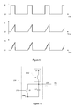

Classifications
-
- H—ELECTRICITY
- H03—ELECTRONIC CIRCUITRY
- H03K—PULSE TECHNIQUE
- H03K9/00—Demodulating pulses which have been modulated with a continuously-variable signal
- H03K9/08—Demodulating pulses which have been modulated with a continuously-variable signal of duration- or width-mudulated pulses or of duty-cycle modulated pulses
-
- H—ELECTRICITY
- H05—ELECTRIC TECHNIQUES NOT OTHERWISE PROVIDED FOR
- H05B—ELECTRIC HEATING; ELECTRIC LIGHT SOURCES NOT OTHERWISE PROVIDED FOR; CIRCUIT ARRANGEMENTS FOR ELECTRIC LIGHT SOURCES, IN GENERAL
- H05B45/00—Circuit arrangements for operating light-emitting diodes [LED]
- H05B45/30—Driver circuits
- H05B45/32—Pulse-control circuits
- H05B45/325—Pulse-width modulation [PWM]
-
- H—ELECTRICITY
- H05—ELECTRIC TECHNIQUES NOT OTHERWISE PROVIDED FOR
- H05B—ELECTRIC HEATING; ELECTRIC LIGHT SOURCES NOT OTHERWISE PROVIDED FOR; CIRCUIT ARRANGEMENTS FOR ELECTRIC LIGHT SOURCES, IN GENERAL
- H05B44/00—Circuit arrangements for operating electroluminescent light sources
-
- H—ELECTRICITY
- H05—ELECTRIC TECHNIQUES NOT OTHERWISE PROVIDED FOR
- H05B—ELECTRIC HEATING; ELECTRIC LIGHT SOURCES NOT OTHERWISE PROVIDED FOR; CIRCUIT ARRANGEMENTS FOR ELECTRIC LIGHT SOURCES, IN GENERAL
- H05B45/00—Circuit arrangements for operating light-emitting diodes [LED]
- H05B45/10—Controlling the intensity of the light
-
- H—ELECTRICITY
- H05—ELECTRIC TECHNIQUES NOT OTHERWISE PROVIDED FOR
- H05B—ELECTRIC HEATING; ELECTRIC LIGHT SOURCES NOT OTHERWISE PROVIDED FOR; CIRCUIT ARRANGEMENTS FOR ELECTRIC LIGHT SOURCES, IN GENERAL
- H05B45/00—Circuit arrangements for operating light-emitting diodes [LED]
- H05B45/30—Driver circuits
- H05B45/37—Converter circuits
- H05B45/3725—Switched mode power supply [SMPS]
-
- H—ELECTRICITY
- H05—ELECTRIC TECHNIQUES NOT OTHERWISE PROVIDED FOR
- H05B—ELECTRIC HEATING; ELECTRIC LIGHT SOURCES NOT OTHERWISE PROVIDED FOR; CIRCUIT ARRANGEMENTS FOR ELECTRIC LIGHT SOURCES, IN GENERAL
- H05B45/00—Circuit arrangements for operating light-emitting diodes [LED]
- H05B45/50—Circuit arrangements for operating light-emitting diodes [LED] responsive to malfunctions or undesirable behaviour of LEDs; responsive to LED life; Protective circuits
- H05B45/59—Circuit arrangements for operating light-emitting diodes [LED] responsive to malfunctions or undesirable behaviour of LEDs; responsive to LED life; Protective circuits for reducing or suppressing flicker or glow effects
-
- H—ELECTRICITY
- H05—ELECTRIC TECHNIQUES NOT OTHERWISE PROVIDED FOR
- H05B—ELECTRIC HEATING; ELECTRIC LIGHT SOURCES NOT OTHERWISE PROVIDED FOR; CIRCUIT ARRANGEMENTS FOR ELECTRIC LIGHT SOURCES, IN GENERAL
- H05B45/00—Circuit arrangements for operating light-emitting diodes [LED]
- H05B45/30—Driver circuits
- H05B45/37—Converter circuits
- H05B45/3725—Switched mode power supply [SMPS]
- H05B45/375—Switched mode power supply [SMPS] using buck topology
-
- H—ELECTRICITY
- H05—ELECTRIC TECHNIQUES NOT OTHERWISE PROVIDED FOR
- H05B—ELECTRIC HEATING; ELECTRIC LIGHT SOURCES NOT OTHERWISE PROVIDED FOR; CIRCUIT ARRANGEMENTS FOR ELECTRIC LIGHT SOURCES, IN GENERAL
- H05B45/00—Circuit arrangements for operating light-emitting diodes [LED]
- H05B45/30—Driver circuits
- H05B45/37—Converter circuits
- H05B45/3725—Switched mode power supply [SMPS]
- H05B45/38—Switched mode power supply [SMPS] using boost topology
-
- H—ELECTRICITY
- H05—ELECTRIC TECHNIQUES NOT OTHERWISE PROVIDED FOR
- H05B—ELECTRIC HEATING; ELECTRIC LIGHT SOURCES NOT OTHERWISE PROVIDED FOR; CIRCUIT ARRANGEMENTS FOR ELECTRIC LIGHT SOURCES, IN GENERAL
- H05B45/00—Circuit arrangements for operating light-emitting diodes [LED]
- H05B45/30—Driver circuits
- H05B45/37—Converter circuits
- H05B45/3725—Switched mode power supply [SMPS]
- H05B45/385—Switched mode power supply [SMPS] using flyback topology
-
- H—ELECTRICITY
- H05—ELECTRIC TECHNIQUES NOT OTHERWISE PROVIDED FOR
- H05B—ELECTRIC HEATING; ELECTRIC LIGHT SOURCES NOT OTHERWISE PROVIDED FOR; CIRCUIT ARRANGEMENTS FOR ELECTRIC LIGHT SOURCES, IN GENERAL
- H05B45/00—Circuit arrangements for operating light-emitting diodes [LED]
- H05B45/30—Driver circuits
- H05B45/37—Converter circuits
- H05B45/3725—Switched mode power supply [SMPS]
- H05B45/39—Circuits containing inverter bridges
-
- H—ELECTRICITY
- H05—ELECTRIC TECHNIQUES NOT OTHERWISE PROVIDED FOR
- H05B—ELECTRIC HEATING; ELECTRIC LIGHT SOURCES NOT OTHERWISE PROVIDED FOR; CIRCUIT ARRANGEMENTS FOR ELECTRIC LIGHT SOURCES, IN GENERAL
- H05B47/00—Circuit arrangements for operating light sources in general, i.e. where the type of light source is not relevant
- H05B47/10—Controlling the light source
Definitions
- the invention relates to control of operation of a driver arranged to drive one or more light emitting diode (LED) light sources.
- embodiments of the invention relate to a driver apparatus and a use of a driver apparatus for providing light intensity control of LED light sources.
- a LED driver typically provides a possibility for controlling the characteristics of the output current provided from the LED driver in order to enable control of light intensity of a LED light source driven by the LED driver.
- the instantaneous level and/or the average level of the output current can be adjusted by issuing an appropriate control signal to the LED driver. Consequently, the light intensity of the LED light source is changed in accordance with the level of the output current.
- the light intensity control may also be referred to as dimming.
- One technique to implement LED dimming is to directly adjust the output current to the desired level within a predetermined range of output currents, typically ranging from a non-zero minimum output current I min to the maximum output current I max .
- Such dimming technique may be based on an analog control signal whose level (e.g. voltage) directly indicates the desired level of the output current.
- This dimming technique is herein referred to as intensity dimming, intensity control or analog dimming. While the intensity control provides straightforward and accurate control of light intensity, drawbacks of this dimming technique include the inability to provide low(est) light intensity levels.
- this dimming technique requires that the LED driver is able to provide the output current at selectable or adjustable level and hence it may not be suitable for all LED drivers, e.g. for LED drivers that are able provide the output current at a fixed predetermined level.
- Another technique to implement LED dimming is to switch the output current between the maximum output current I max and zero current in order to provide the desired average output current.
- a high enough frequency e.g. around 500 to 1000 Hz
- the periods of zero current, causing the light being momentarily switched off are short enough to be unperceivable by a human observer but are rather perceived as reduced light intensity.
- Such dimming technique may be based on a digital control signal, e.g. a Pulse Width Modulation (PWM) signal exhibiting the desired duty cycle D ctrl at a suitable cycle frequency f ctrl .
- PWM Pulse Width Modulation
- Such dimming technique is herein referred to as PWM dimming or PWM control.
- Figure 1a illustrates the concept of PWM dimming.
- the upper curve in Figure 1 a depicts a PWM control signal.
- the PWM control signal applies duty cycle of (approx.) 25 %
- the PWM control signal applies duty cycle of (approx.) 75 %.
- the lower curve of Figure 1a illustrates the corresponding output current.
- the envelope of the output current follows the shape of the PWM control signal.
- the periods of the output current corresponding to the pulses of the PWM control signal (which may also be referred to as active periods of the PWM signal or periods of on-time of the PWM signal) exhibit a high-frequency ripple that results from the switching frequency of a switched-mode power supply typically applied in a power converter unit of a LED driver. It should be noted that while in Figure 1 a the PWM control signal and the resulting output current are depicted as temporally aligned signals (i.e.
- the operation of the LED driver typically causes processing delays that result in a (constant or essentially constant) time shift between the PWM control signal and the output current.
- drawbacks of this technique include perceivable steps in change of light intensity (at least partially due to the switching operation of the switched-mode power converter applied in the LED driver).
- Another drawback is the flickering of light especially at low duty cycles when the pulse width is narrow such that (temporal) distances between the pulses are long enough to result in perceivable periods of the light being momentarily switched off.
- hybrid dimming is a technique that applies a combination of the PWM control and the intensity control.
- hybrid dimming applies both the PWM control and the intensity control at low light intensity levels while at the high light intensity levels only the PWM control with the maximum output current I max (during pulses of the PWM signal) is applied.
- the output current level is set to a lowered value (compared to the maximum output current I max ), thereby enabling usage of higher duty cycle.
- Figure 1b illustrates the concept of hybrid dimming.
- the uppermost curve of Figure 1b depicts the PWM control signal, whereas the curve in the middle depicts the corresponding intensity controls signal. From time t 0 until time t 1 the PWM control signal exhibits duty cycle of (approx.) 50 %, while in the same time period the intensity control signal exhibits signal level that is approx. 50 % of the maximum level. From time t 1 onwards the PWM control signal exhibits duty cycle of (approx.) 75 % while the intensity control signal exhibits the maximum level.
- the lowermost curve of Figure 1b depicts the resulting output current that has an envelope that follows the combined effect of the PWM control signal and the intensity control signal.
- the joint application of PWM control and intensity control techniques contributes to shortening the periods of zero current in the output of the LED driver that correspond to periods between the pulses of the PWM signal (in comparison to pure PWM control) at low light intensity levels. Consequently, the flickering of light at low light intensity levels can be reduced or even eliminated.
- a drawback of the hybrid dimming technique is the additional complexity of the LED driver for jointly operating the PWM control and the intensity control for reaching the desired average output current and hence the desired light intensity level.
- driver apparatus by an arrangement, by a method and by use of the driver apparatus or the arrangement as defined by the respective independent claims.
- an apparatus for providing a driving current for one or more light emitting diodes comprises a power converter portion comprising a switched-mode power converter entity for converting operating power supplied to the apparatus into the driving current in accordance with a driving signal, a driving portion for controlling provision of the driving current from the power converter portion in accordance with the voltage of a dimming control signal, arranged to alternately close and open a first switch of said switched-mode power converter entity at a switching frequency, and a pulse shaping portion for generating the dimming control signal on basis of a PWM signal of lower frequency than said switching frequency, the pulse shaping portion comprising a capacitor configured to receive a charging current and a second switch connected in parallel with the capacitor, the second switch arranged to control provision of the charge from the capacitor as the dimming control signal in accordance with the PWM signal, the pulse shaping portion thereby arranged to derive pulses of the dimming control signal on basis of the PWM signal such that rise time in the pulses of the dimming
- a use of a pulse shaping portion to provide a dimming control signal for a driver arrangement for providing a driving current for one or more light emitting diodes comprising a power converter portion comprising a switched-mode power converter entity for converting operating power supplied to the apparatus into the driving current in accordance with a driving signal and a driving portion for controlling provision of the driving current from the power converter portion in accordance with the voltage of the dimming control signal, arranged to alternately close and open a first switch of said switched-mode power converter entity at a switching frequency, the pulse shaping portion arranged to generate the dimming control signal on basis of a PWM signal of lower frequency than said switching frequency, the pulse shaping portion comprising a capacitor configured to receive a charging current and a second switch connected in parallel with the capacitor, the second switch arranged to control provision of the charge from the capacitor as the dimming control signal in accordance with the PWM signal, the pulse shaping portion thereby arranged to derive pulses of the dimming control
- FIG. 2 schematically illustrates an arrangement comprising a LED driver 220 for driving a LED light source 270.
- the LED driver is coupled to a controller entity 210 for issuing input control signals 205 for controlling operation of the driver 220.
- the LED driver 220 is arranged to derive output current 225 on basis of operating power 217 provided thereto in accordance with the input control signal 205.
- the LED driver 220 is further coupled to the LED light source 270.
- the controller entity 210 may be provided as a single controller entity providing the input control signals 205.
- the controller entity 210 may comprise a number of controller entities that are configured to operate jointly or independently of each other to provide the input control signals 205.
- the controller entity 210 may be arranged to issue the input control signals 205 in response to a user input via a user interface and/or in response to a further control signal received at the controller entity 210 from a further entity.
- the controller entity 210 may, alternatively or additionally, comprise a sensor, such as a PIR sensor or a light sensor, and it may be arranged to issue the control signals 205 in response to sensor measurements in accordance with a (respective) predetermined rule.
- the input control signals 205 may be provided in a number of ways and/or in a number of formats. Typically, however, the input control signal 205 is provided as a command or request in accordance with a lighting control protocol. As an example in this regard, the input control signal 205 may be provided as a control signal providing one or more commands according to the Digital Addressable Lighting Interface (DALI) protocol specified in Appendix E.4 of the International Electrotechnical Commission (IEC) standard 60929, in other words as one or more DALI commands.
- DALI command provided in an input control signal 205 may e.g. specify a desired or requested light intensity level associated with the output current 225, thereby implying a request for a certain average output current 225.
- DALI Digital Addressable Lighting Interface
- IEC International Electrotechnical Commission
- the input control signal 205 may be provided as a control signal comprising one or more commands according to the 1-10 V lighting control signaling, as described/specified in Appendix E.2 of the International Electrotechnical Commission (IEC) standard 60929.
- the voltage of the input control signal 205 may serve as an indication or as a request of the desired light intensity level associated with the output current 225, thereby implying a request for a certain average output current 225.
- the LED light source 270 may comprise a single array of LEDs or, alternatively, two or more arrays of LEDs arranged in parallel.
- An array of LEDs may be referred to as a LED array.
- a LED array comprises either a single LED or two or more LEDs connected in series
- FIG 3 schematically illustrates some components of a LED driver 220 for providing the output current 225 for the LED light source 270.
- the LED driver 220 comprises a pulse shaping portion 230 for generating a dimming control signal 235 on basis of a PWM control signal 215.
- the LED driver 220 further comprises a driving portion 240 for controlling provision of driving current 255 from a power converter portion 250.
- the LED driver 220 further comprises the power converter portion 250 for converting the operating power 217 supplied thereto into the driving current 255 in accordance with a driving signal 245 issued by the driving portion 240.
- the driving current 255 may be provided as the output current 225 or the driving current 255 may be used as basis for providing the output current 225.
- the LED driver 220 is typically provided as a dedicated driver apparatus, embodied by hardware means or as combination of hardware means and software means.
- the LED driver 220 and/or the driver apparatus may comprise further components, portions or units in addition to those described herein. However, role and operation of such components of a LED driver is well known in the art and falls outside the scope of the present invention.
- the arrangement of components depicted in Figure 3 may be considered as use of the pulse control portion 230 for providing the dimming control signal 235 for a LED driving arrangement (or a LED driving apparatus) comprising the driving portion 240 and the power converter portion 250 (possibly together with further components, portions our units typically applied in a LED driver).
- the LED driver 220 may optionally comprise a dimming control interface 212 for generating the PWM control signal 215 on basis of the input control signal 205, e.g. by converting the input control signal 205 into the PWM control signal 215.
- the input control signal 205 may serve as an input signal to the LED driver instead of the PWM control signal 215 (as depicted in Figure 2 ).
- the dimming control interface 212 may be (conceptually) provided as part of the controller entity 210 and hence outside the LED driver 220, thereby making the PWM control signal 215 as an input signal to the LED driver 220 (instead of the input control signal 205).
- the dimming control interface 212 is configured to derive the PWM control signal 215 in accordance with the command or request received in the input control signal 205.
- the dimming control interface 212 is, preferably, configured to generate the PWM control signal 215 and set the duty cycle D ctrl of the PWM control signal 215 in accordance with a command or request received in the input control signal 205.
- This may comprise the dimming control interface 212 to be configured to apply a predetermined mapping, e.g. by employing a mapping function, to convert the requested light intensity level into the corresponding duty cycle D ctrl .
- the requested light intensity level may be indicated e.g. as the desired percentage of the maximum light intensity level L req .
- the applied duty cycle D ctrl typically directly indicates the desired light intensity level as a percentage of the maximum light intensity level.
- the power converter portion 250 is configured to provide the driving current 255 in accordance with the driving signal 245.
- the power converter portion 250 comprises a switched-mode power converter entity configured to convert the operating power 217 provided as input thereto at a first voltage into the driving current 255.
- switched-mode power converters suitable for operating as the power converter entity of the power converter portion 250 are known in the art.
- suitable types of power converter portion include a buck converter, a boost converter, a flyback converter, a half-bridge, etc.
- the driving portion 240 may be configured to control provision of the driving current 255 by issuing the driving signal 245. Consequently, the power converter portion 250 may be configured to convert the operating power 217 supplied thereto into the driving current 255 in accordance with the driving signal 245.
- the driving portion 240 is typically provided as an integrated circuit (IC) or as a processor (such as a microprocessor or a microcontroller)
- the driving portion 240 may be arranged to operate a switch of a switched-mode power converter entity by alternately closing and opening the switch at a high switching frequency (which is typically in range of tens of kilohertz) that depends on the load (e.g. the LED light source 270) driven by the switched-mode power converter entity.
- the timing of opening and closing of the switch is controlled on basis of a current measurement signal received at the driving portion 240, the current measurement signal indicating the observed level of the driving current 255.
- the driving portion 240 may be configured to close the switch in response to the current measurement signal indicating current that is lower than or equal to a low current threshold I TH_lo , thereby causing gradual increase in the output current of the switched-mode power converter.
- the driving portion 240 may be further configured to open the switch in response to the current measurement signal indicating current that is higher than a high current threshold I TH_hi , thereby causing gradual decrease in the output current of the switched-mode power converter. Consequently, the current is caused to (quasi-periodically) vary within bounds defined by the current thresholds I TH_lo and I TH_hi .
- the current thresholds I TH_lo and I TH_hi are set in accordance with a target current I tgt e.g. such the high current threshold I TH_hi may be set to a value that slightly exceeds the target current I tgt , while the low current threshold I TH_lo is set to a value that is slightly smaller than the target current I tgt . Consequently, if the target current I tgt is kept constant, the average level or the rms level of the driving current 255 approximates the target current I tgt .
- the driving portion 240 may be configured to enable and disable the provision of the driving current 255 from the power converter portion 250 in accordance with the voltage of the dimming control signal 235 to implement the PWM dimming technique. This may involve the driving portion 240 controlling the power converter portion 250 to disable provision of the driving current 255 in response to the dimming control signal 235 exhibiting voltage that is smaller than or equal to a predetermined low voltage threshold V TH_lo (i.e. in response to a non-active period of the dimming control signal) and to enable provision of the driving current 255 in response to the dimming control signal 235 exhibiting voltage that is larger than the low voltage threshold V TH_lo (i.e. in response to an active period of the dimming control signal).
- V TH_lo i.e. in response to a non-active period of the dimming control signal
- the operation logic of the driving portion 240 in this regard may be the opposite from the one described above: the driving portion 240 may be configured to disable provision of the driving current 255 in response to the dimming control signal 235 exhibiting voltage that is larger than or equal to the predetermined high voltage threshold V TH_lo and to enable provision of the driving current 255 in response to the dimming control signal 235 exhibiting voltage that is smaller than the low voltage threshold V TH_lo .
- the dimming control signal 235 applied to control PWM dimming does not necessarily have to be a pure PWM signal, but any signal comprising alternating active periods (e.g. exhibiting voltage that is higher than or equal to the low voltage threshold V TH_lo ) and non-active periods (e.g. exhibiting voltage that is smaller than the low voltage threshold V TH_lo , preferably zero or essentially zero) qualifies as the dimming control signal 235. Consequently, the power converter portion 250 provides the output current 255 exhibiting alternating periods of zero current (when disabled) and periods of the driving current 255 approximating the target current I tgt (when enabled).
- the driving portion 240 may be configured to enable analog control of the instantaneous level of the driving current 255, i.e. to enable analog dimming.
- the driving portion 240 may be further configured to control the instantaneous level of the driving current 255 in accordance with the characteristics of the dimming control signal 235.
- the driving portion 240 may be configured to control the target current I tgt in accordance with the dimming control signal 235, e.g. in accordance with the instantaneous voltage of the dimming control signal 235.
- the analog dimming may be implemented for example by the driving portion setting the low and high current thresholds I TH_lo and I TH_hi such that the desired target current I tgt is provided.
- the driving portion 240 is preferably configured to set or adjust the thresholds I TH_lo and I TH_hi only in response to the driving signal 235 exhibiting instantaneous voltage exceeding the low voltage threshold V TH_lo , i.e. voltage that results in enabling the provision of the driving current 255 from the power converter portion 250.
- the driving portion 240 may be configured to control the power converter portion 250 to provide the driving current 255 at an intermediate level that is in the range between a predetermined minimum level I min and a predetermined maximum level I max .
- the applied intermediate level is proportional to the voltage of the dimming control signal 235, in other words the intermediate level increases with increasing voltage of the dimming control signal 235 (and, in contrast, decreases with decreasing voltage of the dimming control signal 235).
- the applied intermediate level may be directly proportional or essentially directly proportional to the voltage of the dimming control signal 235.
- the driving portion 240 may be further configured to control the power converter portion 250 to provide the driving current 255 at the maximum level I max in response to the dimming control signal 235 exhibiting voltage that is higher than or equal to a predetermined high voltage threshold V TH_hi and/or to control the power converter portion 250 to disable provision of the driving current 255 in response to the dimming control signal 235 exhibiting voltage that is lower than or equal to the low voltage threshold V TH_lo .
- the driving portion 240 may be further configured to control the power converter portion 250 to provide the driving current 255 at the intermediate level in response to the dimming control signal 235 exhibiting voltage that is between the low voltage threshold V TH_lo and the high voltage threshold V TH_hi .
- the relationship between the voltage of the dimming control signal 235 and the resulting output current 255 may be the opposite of that of the above example.
- the driving portion 240 may be configured to control the power converter portion 250 to provide the driving current 255 at the intermediate level that is inversely proportional to the voltage of the dimming control signal 235, in other words the intermediate level increases with decreasing voltage of the dimming control signal 235 (and, in contrast, decreases with increasing voltage of the dimming control signal 235).
- the driving portion 240 may be further configured to control the power converter portion 250 to provide the driving current 255 at the maximum level I max in response to the dimming control signal 235 exhibiting voltage that is smaller than or equal to a predetermined low voltage threshold V TH_lo and/or to control the power converter portion 250 to disable provision of the driving current 255 in response to the dimming control signal 235 exhibiting voltage that is higher than or equal to the high voltage threshold V TH_hi , while controlling the power converter portion 250 to provide the driving current 255 at the intermediate level in response to the dimming control signal 235 exhibiting voltage that is between the low voltage threshold V TH_lo and the high voltage threshold V TH_hi .
- the pulse shaping portion 230 is configured to generate the dimming control signal 235 on basis of the PWM control signal 215.
- the PWM control signal 215 is considered as PWM signal in a broad sense, encompassing control signals exhibiting a pulse train of square wave pulses or pulses having essentially square wave shape.
- the pulse shaping portion 230 is configured to process the PWM control signal 215 into the dimming control signal 235 such that the rate (or speed) at which the voltage in the leading edge of pulses of the signal rises towards its maximum value is reduced (in comparison to that of the PWM control signal 215).
- the pulse shaping portion 230 may be configured to provide the dimming control signal 235 where the rate (or speed) at which the voltage in the beginning of pulses rises from the low voltage threshold V TH_lo (or from zero voltage) to the high voltage threshold V TH_hi is reduced.
- the resulting decrease in the slope of the rising edges of the pulses which may also be referred to as softening of the rising edges of the pulses, may hence be applied to cause the rise time in pulses of the dimming control signal 235 to be longer (or slower) than the rise time in the pulses of the PWM control signal 215.
- FIG. 4 An example of the concept of providing the dimming control signal 235 on basis of the PWM control signal 215 together with the resulting driving current 255 is provided in Figure 4 , where the uppermost curve shows an exemplifying PWM control signal 215, the second curve (from the top) shows a respective dimming control signal 235 derived on basis of this PWM control signal, and the lowermost curve shows the resulting driving current 255.
- the PWM control signal applies duty cycle of (approx.) 30 %
- the PWM control signal applies duty cycle of (approx.) 80 %.
- the softened rising edges of the pulses of the dimming control signal 235 slow down the rate of the current level rising towards the maximum level I max in the corresponding portion of the driving current 255.
- the driving portion 240 temporarily disables the provision of the driving current 255 from the power converter portion 250 (or temporarily sets the driving current 255 to a zero current) until the next pulse of the dimming control signal 235. Consequently, due to softened rising edges of the dimming control signal 235 the resulting average current is a smaller portion of the maximum current level I max than indicated by the duty cycle D ctrl of the PWM control signal 215 (whereas in the case of pure PWM dimming the resulting average current typically approximates D ctrl x I max ).
- the duty cycle of (approx.) 30 % applied from time t 0 until time t 1 can be assumed to result in average driving current 255 that is (approx.) 25 % of the maximum level I max
- the duty cycle of (approx.) 80 % can be assumed to result in average driving current 255 that is (approx.) 75 % of the maximum level I max ., thereby resulting in driving current(s) 255 similar to those in the examples of Figures 1 a and 1 b.
- the mapping between the duty cycle of the PWM control signal 215 and the percentage of the maximum current level I max that is descriptive of the average level of the driving current 255 is dependent on the characteristics of the pulse shaping portion 230. Therefore, the mapping function applied in the dimming control interface 212 for converting the requested light intensity into the corresponding duty cycle of the PWM control signal 215 is configured to account for the characteristics of the pulse shaping portion 230.
- This mapping between the requested light intensity L req and the duty cycle D ctrl is applicable to requested light intensities L req that are larger than or equal to a /2.
- the duration of the time period t x and hence the value of a may be e.g. derived on basis of the characteristics of the pulse shaping portion 230 and/or it may be determined on experimental basis.
- This mapping between the requested light intensity L req and the duty cycle D ctrl is applicable to requested light intensities L req that are smaller than or equal to a /2.
- the mapping between the duty cycle D ctrl and the resulting average driving current 255 may be determined on experimental basis e.g. by applying a set of duty cycles covering a range of interest and measuring the resulting average driving currents 255, thereby providing pairs of a duty cycle and the corresponding average driving current 255 that define the mapping.
- the dimming control signal 235 with softened rising edges of the pulses results in the driving current 255 having an envelope that approximates that of the dimming control signal 235.
- this approach results in increased pulse width and hence decreased distances between consecutive pulses when providing the driving current 255 resulting in a certain light intensity level, thereby contributing to reduced perceivable flickering of light due to unnecessarily sparsely provided pulses in the driving current 255 in the low end of the light intensity levels.
- gradually increasing driving current 255 in the beginnings of pulses enable more accurate adjustment of the light intensity level especially in low light intensity levels.
- this approach avoids the complexity of the hybrid dimming while providing performance that is equivalent to that of the hybrid dimming in terms of (avoiding) the flickering of light and (avoiding) perceivable steps in the light intensity change at low light intensity levels.
- Figure 5 provides another example of the dimming control signal 235 with softened rising edges of the pulses.
- the difference to the example of Figure 4 is that this example demonstrates the effect of (even) lower light intensity levels.
- the duty cycle of the PWM control signal 215 (the uppermost curve) is approx. 20 %. Due to softened rising edges of pulses and to relatively low duty cycle, the voltage level in pulses of the dimming control signal 235 (the second curve from the top) does not reach the high voltage threshold V TH_hi before completion of the pulses. Consequently, in the driving current 255 (the lowermost curve) derived on basis of such dimming control signal do not reach the maximum current level I max either.
- the pulse shaping portion 230 may comprise an arrangement of a switch S1 and a capacitor C1 connected in parallel and arranged between the source of the PWM control signal 215 and an input of the driving portion 240, as depicted in example illustrated in Figure 6a .
- the PWM control signal 215 is coupled to control the switch S1, and the low sides of the switch S1 and the capacitor C1 are coupled to a ground potential GND.
- the high sides of the switch S1 and the capacitor C1 are connected to a node 232, which is coupled to the driving portion 240, hence providing the dimming control signal 235 as an output of the pulse shaping portion 230.
- the capacitor C1 is configured to receive a charging current via the node 232.
- the charging current is, preferably, provided as a constant current in order to cause the voltage in the beginnings of pulses of the dimming control signal 235 to increase at constant or essentially constant rate (i.e. to increase linearly over time), thereby facilitating straightforward mapping between the duty cycle in the PWM control signal 215 and the respective average level of the driving current 255 (e.g. as a percentage of the maximum current level I max ).
- the switch S1 is arranged to control provision of the voltage from the capacitor C1 as the dimming control signal 235 (as the output of the pulse shaping portion 230) in accordance with the PWM control signal 215 (serving as an input signal to the pulse shaping portion 230)
- the extent of slowing down is defined by the characteristics, e.g.
- the capacitor C1 may be selected, in view of characteristics of the other components of the LED driver 220, e.g. such that the rise time of pulses of the dimming control signal 235 is set (e.g. slowed down) to a desired value or such that a desired extent of decrease in rise time in pulses of the dimming control signal 235 (in comparison to pulses PWM control signal 215) is provided.
- the switch S1 of the pulse shaping portion 230 may be provided e.g. as a Bipolar Junction Transistor (BJT) transistor or as a Field Effect Transistor (FET) of suitable characteristics.
- Figure 6b schematically illustrates a variant of the pulse shaping portion 230 of Figure 6a employing a npn-type BJT T1 as the switch S1.
- the PWM control signal 215 is coupled to the base of the BJT T1, while the emitter of the BJT T1 is coupled to the ground potential GND and the collector of the BJT T1 is coupled to the node 232.
- a first terminal of the capacitor C1 is connected to the node 232 while a second terminal of the capacitor is coupled to the ground potential GND.
- the current source 242 is coupled to the node 232 to provide the charging current to the first terminal capacitor C1.
- the driver 220 may further comprise charging means coupled to the capacitor C1 and configured to continuously charge the capacitor C1 by the charging current (preferably a constant charging current).
- the charging means is provided by a current source 242 provided in the driving portion 240.
- the charging means may be provided as a dedicated charging arrangement outside the driving portion 240, e.g. as a current source outside the driving portion 240, coupled to the capacitor C1 via the node 232 and arranged to provide the charging current.
- Figure 7a schematically illustrates a pulse shaping portion 230' as a variation of the pulse shaping portion 230.
- the pulse shaping portion 230' comprises a dedicated charging arrangement 242', which comprises a voltage source V1 coupled to the node 232 and hence to the capacitor C1 via a resistor R1.
- the arrangement of the switch S1 and the capacitor C1 as well as operation of the arrangement is similar to that described in context of Figures 6a and 6b . While the structure of the pulse shaping portion 230' is rather straightforward, it is not able to provide a constant charging current (to the capacitor C1), thereby possibly making the mapping between the duty cycle of the PWM control signal 215 and the percentage of the maximum current level I max that is descriptive of the average level of the driving current 255 slightly more complex than e.g. in the example of Figure 6b .
- FIG. 7b schematically illustrates a pulse shaping portion 230", serving as another example of a pulse shaping portion provided outside the driving portion 240.
- the pulse shaping portion 230" comprises a dedicated charging arrangement 242", which comprises a current mirror formed by the BJTs Q1 and Q2.
- the bases of the BJTs Q1 and Q2 are connected to each other and further coupled to a node 243.
- the collectors of the BJTs Q1 and Q2 are also connected to the node 243, and hence connected to each other.
- the node 243 is coupled to the voltage source V2.
- the emitter of the BJT Q1 is coupled via a resistor R2 to the ground potential GND, and the emitter of the BJT Q2 is coupled to the high side of the capacitor C1 via the node 232.
- the arrangement of the switch S1 and the capacitor C1 as well as operation of the arrangement is similar to that described in context of Figures 6a and 6b .
- the pulse shaping portion 230" is able to provide a constant charging current, thereby enabling relatively straightforward mapping between the duty cycle of the PWM control signal 215 and the percentage of the maximum current level I max that is descriptive of the average level of the driving current 255.
- the arrangement of the capacitor C1 and the switch S1 connected in parallel exemplified by circuits of Figure 6 and 7 is arranged to provide the dimming control signal 235 such that when the PWM control signal 215 is in active state (in 'high' state during a pulse of the PWM control signal 215, e.g. exhibiting a voltage exceeding a predefined threshold), the switch S1 is closed and electric current flows via the switch S1, and the voltage at the high side of the capacitor S1 is a (low) voltage that depends on characteristics of the switch S1. Consequently, the dimming control signal 235 at low voltage is provided. E.g. in case the switch S1 is provided as a BJT, this voltage is the threshold voltage of the BJT.
- the PWM control signal 215 when the PWM control signal 215 is in non-active state (in 'low' state between pulses of the PWM control signal 215, e.g. exhibiting a voltage not exceeding the predefined threshold) the electric current flows via the capacitor C1, thereby charging the capacitor C1. This results in the voltage at the high side of the capacitor C1 to gradually increase towards a maximum value that depends on characteristics (e.g. capacitance) of the capacitor C1. Consequently, the dimming control signal 235 of gradually increasing voltage is provided. Once the PWM control signal 215 is again switched to the active state (to commence the next pulse of the PWM control signal 215), the capacitor C1 is quickly discharged and the resulting dimming control signal 235 is again provided at the low voltage.
- the pulse shaping portion according to Figures 6a , 6b , 7 in practice operates to invert the PWM controls signal 215 such that active periods (i.e. pulses) of the PWM control signal 215 are converted into non-active periods (i.e. periods between pulses) of the dimming control signal 235 while at the same time causing the rise time in pulses of the dimming control signal 235 to be longer (or slower) than the rise time in the pulses of the PWM control signal 215.
- Figure 8 illustrates this effect by showing an exemplifying PWM control signal 215 (the topmost curve) which is an inverse of that of the example of Figure 4 , whereas the resulting dimming control signal 235 (the second curve from the top) and the driving current 255 (the lowermost curve) are similar to those of the example of Figure 4 . Due the pulse control portion 230 e.g.
- the dimming control interface 212 must be configured, in view of such 'inverting' behavior of the pulse shaping portion 230, to apply a mapping function that takes both the 'inversion' of the pulses and the softening of the rising edges of pulses into account in determination of the duty cycle D ctrl for the PWM control signal 215 on basis of the desired light intensity level L req .
- the mapping between the requested light intensity level L req the duty cycle D ctrl of the PWM control signal 215 may be determined e.g.
- D ctrl 100 % - L req - a /2
- the term '100 % - L req ' represents the 'inversion' of the pulses of the PWM control signal 215 in the pulse shaping portion 230 while the term a /2 represents the contribution of the softening of the rising edges of pulses (as described hereinbefore in more detail).
- mapping between the duty cycle D ctrl and the resulting average driving current 255 on experimental basis described hereinbefore may be applied also for the case where the pulse control portion 230 'inverts' the pulses of the PWM control signal 215 in the process of generating the dimming control signal 235.
Landscapes
- Physics & Mathematics (AREA)
- Engineering & Computer Science (AREA)
- Microelectronics & Electronic Packaging (AREA)
- Optics & Photonics (AREA)
- Circuit Arrangement For Electric Light Sources In General (AREA)
Abstract
Description
- The invention relates to control of operation of a driver arranged to drive one or more light emitting diode (LED) light sources. In particular, embodiments of the invention relate to a driver apparatus and a use of a driver apparatus for providing light intensity control of LED light sources.
- A LED driver typically provides a possibility for controlling the characteristics of the output current provided from the LED driver in order to enable control of light intensity of a LED light source driven by the LED driver. Typically, the instantaneous level and/or the average level of the output current can be adjusted by issuing an appropriate control signal to the LED driver. Consequently, the light intensity of the LED light source is changed in accordance with the level of the output current. The light intensity control may also be referred to as dimming.
- One technique to implement LED dimming is to directly adjust the output current to the desired level within a predetermined range of output currents, typically ranging from a non-zero minimum output current I min to the maximum output current I max. Such dimming technique may be based on an analog control signal whose level (e.g. voltage) directly indicates the desired level of the output current. This dimming technique is herein referred to as intensity dimming, intensity control or analog dimming. While the intensity control provides straightforward and accurate control of light intensity, drawbacks of this dimming technique include the inability to provide low(est) light intensity levels. Moreover, this dimming technique requires that the LED driver is able to provide the output current at selectable or adjustable level and hence it may not be suitable for all LED drivers, e.g. for LED drivers that are able provide the output current at a fixed predetermined level.
- Another technique to implement LED dimming is to switch the output current between the maximum output current I max and zero current in order to provide the desired average output current. When switched at a high enough frequency (e.g. around 500 to 1000 Hz), the periods of zero current, causing the light being momentarily switched off, are short enough to be unperceivable by a human observer but are rather perceived as reduced light intensity. Such dimming technique may be based on a digital control signal, e.g. a Pulse Width Modulation (PWM) signal exhibiting the desired duty cycle D ctrl at a suitable cycle frequency f ctrl. Consequently, the envelope of the output current may be arranged to follow or approximate the PWM signal and the resulting average output current follows or approximates the duty cycle such that the average output current approximates I avg = D ctrl x I max. Such dimming technique is herein referred to as PWM dimming or PWM control.
-
Figure 1a illustrates the concept of PWM dimming. The upper curve inFigure 1 a depicts a PWM control signal. In this example, from time t0 until time t1 the PWM control signal applies duty cycle of (approx.) 25 %, whereas from time t1 onwards the PWM control signal applies duty cycle of (approx.) 75 %. The lower curve ofFigure 1a illustrates the corresponding output current. As can be seen inFigure 1a , the envelope of the output current follows the shape of the PWM control signal. The periods of the output current corresponding to the pulses of the PWM control signal (which may also be referred to as active periods of the PWM signal or periods of on-time of the PWM signal) exhibit a high-frequency ripple that results from the switching frequency of a switched-mode power supply typically applied in a power converter unit of a LED driver. It should be noted that while inFigure 1 a the PWM control signal and the resulting output current are depicted as temporally aligned signals (i.e. the beginnings of the pulses in the output current are temporally aligned with the corresponding pulses of the PWM control signal), in a real-life scenario the operation of the LED driver typically causes processing delays that result in a (constant or essentially constant) time shift between the PWM control signal and the output current. - While the PWM dimming provides a straightforward technique for controlling the light intensity and also enables controlling light intensity levels provided using a LED driver that applies a fixed predetermined output current level, drawbacks of this technique include perceivable steps in change of light intensity (at least partially due to the switching operation of the switched-mode power converter applied in the LED driver). Another drawback is the flickering of light especially at low duty cycles when the pulse width is narrow such that (temporal) distances between the pulses are long enough to result in perceivable periods of the light being momentarily switched off.
- To at least partially address the drawbacks of the PWM dimming and the intensity control, a hybrid dimming may be applied. The hybrid dimming is a technique that applies a combination of the PWM control and the intensity control. Typically, hybrid dimming applies both the PWM control and the intensity control at low light intensity levels while at the high light intensity levels only the PWM control with the maximum output current I max (during pulses of the PWM signal) is applied. In particular, at the low light intensity levels the output current level is set to a lowered value (compared to the maximum output current I max), thereby enabling usage of higher duty cycle.
-
Figure 1b illustrates the concept of hybrid dimming. The uppermost curve ofFigure 1b depicts the PWM control signal, whereas the curve in the middle depicts the corresponding intensity controls signal. From time t0 until time t1 the PWM control signal exhibits duty cycle of (approx.) 50 %, while in the same time period the intensity control signal exhibits signal level that is approx. 50 % of the maximum level. From time t1 onwards the PWM control signal exhibits duty cycle of (approx.) 75 % while the intensity control signal exhibits the maximum level. The lowermost curve ofFigure 1b depicts the resulting output current that has an envelope that follows the combined effect of the PWM control signal and the intensity control signal. When compared to the example ofFigure 1a , now the output current within the period from time t0 to time t1 is approx. half of that of the example ofFigure 1 a. On the other hand, the durations of the non-zero current periods are approx. twice those of the corresponding periods of the example ofFigure 1 a. Consequently, the average output current of the example ofFigure 1b is similar to that of the example ofFigure 1 a. From time t1 onwards, both the control signal and the resulting output current of the example ofFigure 1b are similar to those of the example ofFigure 1 a. - The joint application of PWM control and intensity control techniques contributes to shortening the periods of zero current in the output of the LED driver that correspond to periods between the pulses of the PWM signal (in comparison to pure PWM control) at low light intensity levels. Consequently, the flickering of light at low light intensity levels can be reduced or even eliminated. However, a drawback of the hybrid dimming technique is the additional complexity of the LED driver for jointly operating the PWM control and the intensity control for reaching the desired average output current and hence the desired light intensity level.
- Consequently, it is an object of the present invention to provide a dimming technique for LED light sources that enables straightforward control of light intensity level at a reasonable complexity, enables applying wide range of light intensity levels while at the same also contributes to avoiding perceivable flickering of light at low light intensity levels.
- The objects of the invention are reached by a driver apparatus, by an arrangement, by a method and by use of the driver apparatus or the arrangement as defined by the respective independent claims.
- According to a first example embodiment, an apparatus for providing a driving current for one or more light emitting diodes is provided. The apparatus comprises a power converter portion comprising a switched-mode power converter entity for converting operating power supplied to the apparatus into the driving current in accordance with a driving signal, a driving portion for controlling provision of the driving current from the power converter portion in accordance with the voltage of a dimming control signal, arranged to alternately close and open a first switch of said switched-mode power converter entity at a switching frequency, and a pulse shaping portion for generating the dimming control signal on basis of a PWM signal of lower frequency than said switching frequency, the pulse shaping portion comprising a capacitor configured to receive a charging current and a second switch connected in parallel with the capacitor, the second switch arranged to control provision of the charge from the capacitor as the dimming control signal in accordance with the PWM signal, the pulse shaping portion thereby arranged to derive pulses of the dimming control signal on basis of the PWM signal such that rise time in the pulses of the dimming control signal is longer than that of the pulses of the PWM signal.
- According to a second example embodiment, a use of a pulse shaping portion to provide a dimming control signal for a driver arrangement for providing a driving current for one or more light emitting diodes is provided, the driving arrangement comprising a power converter portion comprising a switched-mode power converter entity for converting operating power supplied to the apparatus into the driving current in accordance with a driving signal and a driving portion for controlling provision of the driving current from the power converter portion in accordance with the voltage of the dimming control signal, arranged to alternately close and open a first switch of said switched-mode power converter entity at a switching frequency, the pulse shaping portion arranged to generate the dimming control signal on basis of a PWM signal of lower frequency than said switching frequency, the pulse shaping portion comprising a capacitor configured to receive a charging current and a second switch connected in parallel with the capacitor, the second switch arranged to control provision of the charge from the capacitor as the dimming control signal in accordance with the PWM signal, the pulse shaping portion thereby arranged to derive pulses of the dimming control signal on basis of the PWM signal such that rise time in the pulses of the dimming control signal is longer than that of the pulses of the PWM signal.
- The exemplifying embodiments of the invention presented in this patent application are not to be interpreted to pose limitations to the applicability of the appended claims. The verb "to comprise" and its derivatives are used in this patent application as an open limitation that does not exclude the existence of also unrecited features. The features described hereinafter are mutually freely combinable unless explicitly stated otherwise.
- The novel features which are considered as characteristic of the invention are set forth in particular in the appended claims. The invention itself, however, both as to its construction and its method of operation, together with additional objects and advantages thereof, will be best understood from the following detailed description of specific embodiments when read in connection with the accompanying drawings.
- Some embodiments of the invention are illustrated by way of example, and not by way of limitation, in the figures of the accompanying drawings.
-
Figure 1 a illustrates the concept of PWM dimming. -
Figure 1b illustrates the concept of hybrid dimming. -
Figure 2 schematically illustrates an arrangement comprising a LED driver in accordance with an embodiment of the invention. -
Figure 3 schematically illustrates some components of a LED driver in accordance with an embodiment of the invention. -
Figure 4 illustrates the dimming in accordance with an embodiment of the invention. -
Figure 5 illustrates the dimming in accordance with an embodiment of the invention. -
Figure 6a schematically illustrates a pulse shaping portion in accordance with an embodiment of the invention. -
Figure 6b schematically illustrates a pulse shaping portion in accordance with an embodiment of the invention. -
Figure 7a schematically illustrates a pulse shaping portion in accordance with an embodiment of the invention. -
Figure 7b schematically illustrates a pulse shaping portion in accordance with an embodiment of the invention. -
Figure 8 illustrates the dimming in accordance with an embodiment of the invention. -
Figure 2 schematically illustrates an arrangement comprising aLED driver 220 for driving aLED light source 270. In the example arrangement depicted inFigure 2 , the LED driver is coupled to acontroller entity 210 for issuing input control signals 205 for controlling operation of thedriver 220. TheLED driver 220 is arranged to derive output current 225 on basis of operatingpower 217 provided thereto in accordance with theinput control signal 205. TheLED driver 220 is further coupled to the LEDlight source 270. - The
controller entity 210 may be provided as a single controller entity providing the input control signals 205. Alternatively, although depicted as a single entity inFigure 2 , thecontroller entity 210 may comprise a number of controller entities that are configured to operate jointly or independently of each other to provide the input control signals 205. Thecontroller entity 210 may be arranged to issue the input control signals 205 in response to a user input via a user interface and/or in response to a further control signal received at thecontroller entity 210 from a further entity. Thecontroller entity 210 may, alternatively or additionally, comprise a sensor, such as a PIR sensor or a light sensor, and it may be arranged to issue the control signals 205 in response to sensor measurements in accordance with a (respective) predetermined rule. - The input control signals 205 may be provided in a number of ways and/or in a number of formats. Typically, however, the
input control signal 205 is provided as a command or request in accordance with a lighting control protocol. As an example in this regard, theinput control signal 205 may be provided as a control signal providing one or more commands according to the Digital Addressable Lighting Interface (DALI) protocol specified in Appendix E.4 of the International Electrotechnical Commission (IEC) standard 60929, in other words as one or more DALI commands. A DALI command provided in aninput control signal 205 may e.g. specify a desired or requested light intensity level associated with the output current 225, thereby implying a request for a certain average output current 225. - As a further example, the
input control signal 205 may be provided as a control signal comprising one or more commands according to the 1-10 V lighting control signaling, as described/specified in Appendix E.2 of the International Electrotechnical Commission (IEC) standard 60929. In such a signal the voltage of theinput control signal 205 may serve as an indication or as a request of the desired light intensity level associated with the output current 225, thereby implying a request for a certain average output current 225. - Although illustrated as a single entity, the LED
light source 270 may comprise a single array of LEDs or, alternatively, two or more arrays of LEDs arranged in parallel. An array of LEDs may be referred to as a LED array. A LED array comprises either a single LED or two or more LEDs connected in series -
Figure 3 schematically illustrates some components of aLED driver 220 for providing the output current 225 for the LEDlight source 270. TheLED driver 220 comprises apulse shaping portion 230 for generating adimming control signal 235 on basis of aPWM control signal 215. TheLED driver 220 further comprises a drivingportion 240 for controlling provision of driving current 255 from apower converter portion 250. TheLED driver 220 further comprises thepower converter portion 250 for converting the operatingpower 217 supplied thereto into the driving current 255 in accordance with a drivingsignal 245 issued by the drivingportion 240. The driving current 255 may be provided as the output current 225 or the driving current 255 may be used as basis for providing theoutput current 225. TheLED driver 220 is typically provided as a dedicated driver apparatus, embodied by hardware means or as combination of hardware means and software means. TheLED driver 220 and/or the driver apparatus may comprise further components, portions or units in addition to those described herein. However, role and operation of such components of a LED driver is well known in the art and falls outside the scope of the present invention. Alternatively, the arrangement of components depicted inFigure 3 may be considered as use of thepulse control portion 230 for providing the dimmingcontrol signal 235 for a LED driving arrangement (or a LED driving apparatus) comprising the drivingportion 240 and the power converter portion 250 (possibly together with further components, portions our units typically applied in a LED driver). - In case the
input control signal 205 is provided as commands or requests in accordance with a lighting control protocol, theLED driver 220 may optionally comprise adimming control interface 212 for generating thePWM control signal 215 on basis of theinput control signal 205, e.g. by converting theinput control signal 205 into thePWM control signal 215. In such a scenario theinput control signal 205 may serve as an input signal to the LED driver instead of the PWM control signal 215 (as depicted inFigure 2 ). Alternatively, the dimmingcontrol interface 212 may be (conceptually) provided as part of thecontroller entity 210 and hence outside theLED driver 220, thereby making thePWM control signal 215 as an input signal to the LED driver 220 (instead of the input control signal 205). - The dimming
control interface 212 is configured to derive thePWM control signal 215 in accordance with the command or request received in theinput control signal 205. The dimmingcontrol interface 212 is, preferably, configured to generate thePWM control signal 215 and set the duty cycle D ctrl of thePWM control signal 215 in accordance with a command or request received in theinput control signal 205. This may comprise thedimming control interface 212 to be configured to apply a predetermined mapping, e.g. by employing a mapping function, to convert the requested light intensity level into the corresponding duty cycle D ctrl. The requested light intensity level may be indicated e.g. as the desired percentage of the maximum light intensity level L req. Consequently, the mapping function may cause thedimming control interface 212 to set the duty cycle D ctrl of thePWM control signal 215 to D ctrl = L req. Hence, in such an arrangement the applied duty cycle D ctrl typically directly indicates the desired light intensity level as a percentage of the maximum light intensity level. Such control of light intensity level in LED drivers is well known in the art. - The
power converter portion 250 is configured to provide the driving current 255 in accordance with the drivingsignal 245. Thepower converter portion 250 comprises a switched-mode power converter entity configured to convert theoperating power 217 provided as input thereto at a first voltage into the driving current 255. A number of different switched-mode power converters suitable for operating as the power converter entity of thepower converter portion 250 are known in the art. Non-limiting examples of suitable types of power converter portion include a buck converter, a boost converter, a flyback converter, a half-bridge, etc. - The driving
portion 240 may be configured to control provision of the driving current 255 by issuing the drivingsignal 245. Consequently, thepower converter portion 250 may be configured to convert theoperating power 217 supplied thereto into the driving current 255 in accordance with the drivingsignal 245. The drivingportion 240 is typically provided as an integrated circuit (IC) or as a processor (such as a microprocessor or a microcontroller) In this regard, the drivingportion 240 may be arranged to operate a switch of a switched-mode power converter entity by alternately closing and opening the switch at a high switching frequency (which is typically in range of tens of kilohertz) that depends on the load (e.g. the LED light source 270) driven by the switched-mode power converter entity. The timing of opening and closing of the switch is controlled on basis of a current measurement signal received at the drivingportion 240, the current measurement signal indicating the observed level of the driving current 255. As an example in this regard, the drivingportion 240 may be configured to close the switch in response to the current measurement signal indicating current that is lower than or equal to a low current threshold I TH_lo, thereby causing gradual increase in the output current of the switched-mode power converter. In contrast, the drivingportion 240 may be further configured to open the switch in response to the current measurement signal indicating current that is higher than a high current threshold I TH_hi, thereby causing gradual decrease in the output current of the switched-mode power converter. Consequently, the current is caused to (quasi-periodically) vary within bounds defined by the current thresholds I TH_lo and I TH_hi. - The current thresholds I TH_lo and I TH_hi are set in accordance with a target current I tgt e.g. such the high current threshold I TH_hi may be set to a value that slightly exceeds the target current I tgt, while the low current threshold I TH_lo is set to a value that is slightly smaller than the target current I tgt. Consequently, if the target current I tgt is kept constant, the average level or the rms level of the driving current 255 approximates the target current I tgt.
- The driving
portion 240 may be configured to enable and disable the provision of the driving current 255 from thepower converter portion 250 in accordance with the voltage of the dimmingcontrol signal 235 to implement the PWM dimming technique. This may involve the drivingportion 240 controlling thepower converter portion 250 to disable provision of the driving current 255 in response to the dimmingcontrol signal 235 exhibiting voltage that is smaller than or equal to a predetermined low voltage threshold V TH_lo (i.e. in response to a non-active period of the dimming control signal) and to enable provision of the driving current 255 in response to the dimmingcontrol signal 235 exhibiting voltage that is larger than the low voltage threshold V TH_lo (i.e. in response to an active period of the dimming control signal). Alternatively, the operation logic of the drivingportion 240 in this regard may be the opposite from the one described above: the drivingportion 240 may be configured to disable provision of the driving current 255 in response to the dimmingcontrol signal 235 exhibiting voltage that is larger than or equal to the predetermined high voltage threshold V TH_lo and to enable provision of the driving current 255 in response to the dimmingcontrol signal 235 exhibiting voltage that is smaller than the low voltage threshold V TH_lo. - The dimming
control signal 235 applied to control PWM dimming does not necessarily have to be a pure PWM signal, but any signal comprising alternating active periods (e.g. exhibiting voltage that is higher than or equal to the low voltage threshold V TH_lo) and non-active periods (e.g. exhibiting voltage that is smaller than the low voltage threshold V TH_lo, preferably zero or essentially zero) qualifies as the dimmingcontrol signal 235. Consequently, thepower converter portion 250 provides the output current 255 exhibiting alternating periods of zero current (when disabled) and periods of the driving current 255 approximating the target current I tgt (when enabled). - The driving
portion 240 may be configured to enable analog control of the instantaneous level of the driving current 255, i.e. to enable analog dimming. In this regard, the drivingportion 240 may be further configured to control the instantaneous level of the driving current 255 in accordance with the characteristics of the dimmingcontrol signal 235. To this end, the drivingportion 240 may be configured to control the target current I tgt in accordance with the dimmingcontrol signal 235, e.g. in accordance with the instantaneous voltage of the dimmingcontrol signal 235. - The analog dimming may be implemented for example by the driving portion setting the low and high current thresholds I TH_lo and I TH_hi such that the desired target current I tgt is provided. The driving
portion 240 is preferably configured to set or adjust the thresholds I TH_lo and I TH_hi only in response to thedriving signal 235 exhibiting instantaneous voltage exceeding the low voltage threshold V TH_lo, i.e. voltage that results in enabling the provision of the driving current 255 from thepower converter portion 250. - The driving
portion 240 may be configured to control thepower converter portion 250 to provide the driving current 255 at an intermediate level that is in the range between a predetermined minimum level I min and a predetermined maximum level I max. The applied intermediate level is proportional to the voltage of the dimmingcontrol signal 235, in other words the intermediate level increases with increasing voltage of the dimming control signal 235 (and, in contrast, decreases with decreasing voltage of the dimming control signal 235). In particular, the applied intermediate level may be directly proportional or essentially directly proportional to the voltage of the dimmingcontrol signal 235. - Moreover, the driving
portion 240 may be further configured to control thepower converter portion 250 to provide the driving current 255 at the maximum level I max in response to the dimmingcontrol signal 235 exhibiting voltage that is higher than or equal to a predetermined high voltage threshold V TH_hi and/or to control thepower converter portion 250 to disable provision of the driving current 255 in response to the dimmingcontrol signal 235 exhibiting voltage that is lower than or equal to the low voltage threshold V TH_lo. Furthermore, the drivingportion 240 may be further configured to control thepower converter portion 250 to provide the driving current 255 at the intermediate level in response to the dimmingcontrol signal 235 exhibiting voltage that is between the low voltage threshold V TH_lo and the high voltage threshold V TH_hi. - Alternatively (as described for the PWM dimming technique above), the relationship between the voltage of the dimming
control signal 235 and the resulting output current 255 may be the opposite of that of the above example. In other words, the drivingportion 240 may be configured to control thepower converter portion 250 to provide the driving current 255 at the intermediate level that is inversely proportional to the voltage of the dimmingcontrol signal 235, in other words the intermediate level increases with decreasing voltage of the dimming control signal 235 (and, in contrast, decreases with increasing voltage of the dimming control signal 235). Consequently, in such a scenario the drivingportion 240 may be further configured to control thepower converter portion 250 to provide the driving current 255 at the maximum level I max in response to the dimmingcontrol signal 235 exhibiting voltage that is smaller than or equal to a predetermined low voltage threshold V TH_lo and/or to control thepower converter portion 250 to disable provision of the driving current 255 in response to the dimmingcontrol signal 235 exhibiting voltage that is higher than or equal to the high voltage threshold V TH_hi, while controlling thepower converter portion 250 to provide the driving current 255 at the intermediate level in response to the dimmingcontrol signal 235 exhibiting voltage that is between the low voltage threshold V TH_lo and the high voltage threshold V TH_hi. - The
pulse shaping portion 230 is configured to generate the dimmingcontrol signal 235 on basis of thePWM control signal 215. Herein, thePWM control signal 215 is considered as PWM signal in a broad sense, encompassing control signals exhibiting a pulse train of square wave pulses or pulses having essentially square wave shape. Thepulse shaping portion 230 is configured to process thePWM control signal 215 into the dimmingcontrol signal 235 such that the rate (or speed) at which the voltage in the leading edge of pulses of the signal rises towards its maximum value is reduced (in comparison to that of the PWM control signal 215). In particular, thepulse shaping portion 230 may be configured to provide thedimming control signal 235 where the rate (or speed) at which the voltage in the beginning of pulses rises from the low voltage threshold V TH_lo (or from zero voltage) to the high voltage threshold V TH_hi is reduced. The resulting decrease in the slope of the rising edges of the pulses, which may also be referred to as softening of the rising edges of the pulses, may hence be applied to cause the rise time in pulses of the dimmingcontrol signal 235 to be longer (or slower) than the rise time in the pulses of thePWM control signal 215. - An example of the concept of providing the dimming
control signal 235 on basis of thePWM control signal 215 together with the resulting driving current 255 is provided inFigure 4 , where the uppermost curve shows an exemplifyingPWM control signal 215, the second curve (from the top) shows a respectivedimming control signal 235 derived on basis of this PWM control signal, and the lowermost curve shows the resulting driving current 255. In this example, from time t0 until time t1 the PWM control signal applies duty cycle of (approx.) 30 %, whereas from time t1 onwards the PWM control signal applies duty cycle of (approx.) 80 %. As can be seen inFigure 4 , the softened rising edges of the pulses of the dimmingcontrol signal 235 slow down the rate of the current level rising towards the maximum level I max in the corresponding portion of the driving current 255. This is due to the operation of the drivingportion 240, controlling thepower converter portion 250 to provide the driving current 255 at the minimum level I min once the voltage of the dimmingcontrol signal 235 has reached the low voltage threshold V TH_lo and controlling thepower converter portion 250 to increase the level of the driving current 255 with the increasing voltage of thediming control signal 235 until reaching the maximum level I max.. Subsequently, upon completion of the pulse of the dimmingcontrol signal 235, the drivingportion 240 temporarily disables the provision of the driving current 255 from the power converter portion 250 (or temporarily sets the driving current 255 to a zero current) until the next pulse of the dimmingcontrol signal 235. Consequently, due to softened rising edges of the dimmingcontrol signal 235 the resulting average current is a smaller portion of the maximum current level I max than indicated by the duty cycle D ctrl of the PWM control signal 215 (whereas in the case of pure PWM dimming the resulting average current typically approximates D ctrl x I max). To exemplify this effect, the duty cycle of (approx.) 30 % applied from time t0 until time t1 can be assumed to result in average driving current 255 that is (approx.) 25 % of the maximum level I max, wherein the duty cycle of (approx.) 80 % can be assumed to result in average driving current 255 that is (approx.) 75 % of the maximum level I max., thereby resulting in driving current(s) 255 similar to those in the examples ofFigures 1 a and 1 b. The mapping between the duty cycle of thePWM control signal 215 and the percentage of the maximum current level I max that is descriptive of the average level of the driving current 255 is dependent on the characteristics of thepulse shaping portion 230. Therefore, the mapping function applied in thedimming control interface 212 for converting the requested light intensity into the corresponding duty cycle of thePWM control signal 215 is configured to account for the characteristics of thepulse shaping portion 230. - As an example in this regard, one may assume that in the beginning of pulses of dimming
control signal 235 the voltage increases at a constant or essentially constant rate, that the rise time for the voltage to rise from the low voltage threshold V TH_lo to the high voltage threshold V TH_hi is t x, and that the voltage stays at or above the high threshold V TH_hi until the end of the pulse. Further assuming that the overall duration of pulse (when the voltage is at or above V TH_hi) is t a and that the overall duration of the cycle is t c, the driving current 255 can be assumed to rise linearly from zero to I max during the time period t x in the beginning of a pulse, to stay at I max until the end of the pulse, and to drop to zero at the end of the pulse. Consequently, if denoting a = t x / t c and b = ta / t c, the average current of the cycle (and over a sequence of such cycles) becomes I avg = (b - a/2) x I max. Hence, in in order to provide thedimming control signal 235 resulting in an average current that is L req times the maximum current I max (i.e. L req x I max), thePWM control signal 215 should exhibit the duty cycle D ctrl = L req + a/2. This mapping between the requested light intensity L req and the duty cycle D ctrl is applicable to requested light intensities L req that are larger than or equal to a/2. The duration of the time period t x and hence the value of a may be e.g. derived on basis of the characteristics of thepulse shaping portion 230 and/or it may be determined on experimental basis. As an example, if the desired percentage of the maximum light intensity is 25 % (i.e. L req = 0.25) and I max is reached after 10 % of a pulse duration (i.e. a = 0.1), the duty cycle D ctrl for thePWM control signal 215 should be set to D ctrl = 0.25 + 0.1 / 2 = 0.3. - While the above logic describes the relationship between the requested light intensity L req and the required duty cycle D ctrl for the case where pulse duration of the
PWM control signal 215 is long enough to enable reaching the maximum current I max, i.e. longer than t x, the relationship is slightly different in the case where pulse duration is shorter than t x. In this case the current reached before termination of the pulse is b/a x I max (where b < a) and hence the average current over a pulse is b/(2a) x I max and the average current over the cycle (and over a sequence of such cycles) is b 2/(2a) x I max. Hence, in order to provide thedimming control signal 235 resulting in an average current that is L req times the maximum current I max (i.e. L req x I max), thePWM control signal 215 should exhibit the duty cycle D ctrl = sqrt(2a x L req), where sqrt() denotes the square root operation. This mapping between the requested light intensity L req and the duty cycle D ctrl is applicable to requested light intensities L req that are smaller than or equal to a/2. As an example, if the desired percentage of the maximum light intensity is 4 % (i.e. L req = 0.04) and a = 0.1, the duty cycle D ctrl for thePWM control signal 215 should be set to D ctrl = sqrt(2 x 0.1 x 0.04) ≈ 0.089. - Alternatively, especially in case the voltage in the beginning of the pulses increases at non-constant rate, the mapping between the duty cycle D ctrl and the resulting average driving current 255 may be determined on experimental basis e.g. by applying a set of duty cycles covering a range of interest and measuring the resulting average driving currents 255, thereby providing pairs of a duty cycle and the corresponding average driving current 255 that define the mapping.
- As
Figure 4 demonstrates, the dimmingcontrol signal 235 with softened rising edges of the pulses results in the driving current 255 having an envelope that approximates that of the dimmingcontrol signal 235. In comparison to pure PWM dimming, this approach results in increased pulse width and hence decreased distances between consecutive pulses when providing the driving current 255 resulting in a certain light intensity level, thereby contributing to reduced perceivable flickering of light due to unnecessarily sparsely provided pulses in the driving current 255 in the low end of the light intensity levels. Moreover, gradually increasing driving current 255 in the beginnings of pulses enable more accurate adjustment of the light intensity level especially in low light intensity levels. On the other hand, at the same time this approach avoids the complexity of the hybrid dimming while providing performance that is equivalent to that of the hybrid dimming in terms of (avoiding) the flickering of light and (avoiding) perceivable steps in the light intensity change at low light intensity levels. -
Figure 5 provides another example of the dimmingcontrol signal 235 with softened rising edges of the pulses. The difference to the example ofFigure 4 is that this example demonstrates the effect of (even) lower light intensity levels. In the example ofFigure 5 , the duty cycle of the PWM control signal 215 (the uppermost curve) is approx. 20 %. Due to softened rising edges of pulses and to relatively low duty cycle, the voltage level in pulses of the dimming control signal 235 (the second curve from the top) does not reach the high voltage threshold V TH_hi before completion of the pulses. Consequently, in the driving current 255 (the lowermost curve) derived on basis of such dimming control signal do not reach the maximum current level I max either. - The
pulse shaping portion 230 may comprise an arrangement of a switch S1 and a capacitor C1 connected in parallel and arranged between the source of thePWM control signal 215 and an input of the drivingportion 240, as depicted in example illustrated inFigure 6a . ThePWM control signal 215 is coupled to control the switch S1, and the low sides of the switch S1 and the capacitor C1 are coupled to a ground potential GND. The high sides of the switch S1 and the capacitor C1 are connected to anode 232, which is coupled to the drivingportion 240, hence providing the dimmingcontrol signal 235 as an output of thepulse shaping portion 230. The capacitor C1 is configured to receive a charging current via thenode 232. The charging current is, preferably, provided as a constant current in order to cause the voltage in the beginnings of pulses of the dimmingcontrol signal 235 to increase at constant or essentially constant rate (i.e. to increase linearly over time), thereby facilitating straightforward mapping between the duty cycle in thePWM control signal 215 and the respective average level of the driving current 255 (e.g. as a percentage of the maximum current level I max). The switch S1 is arranged to control provision of the voltage from the capacitor C1 as the dimming control signal 235 (as the output of the pulse shaping portion 230) in accordance with the PWM control signal 215 (serving as an input signal to the pulse shaping portion 230) The extent of slowing down is defined by the characteristics, e.g. the capacitance, of the capacitor. Hence, the capacitor C1 may be selected, in view of characteristics of the other components of theLED driver 220, e.g. such that the rise time of pulses of the dimmingcontrol signal 235 is set (e.g. slowed down) to a desired value or such that a desired extent of decrease in rise time in pulses of the dimming control signal 235 (in comparison to pulses PWM control signal 215) is provided. - As an example, the switch S1 of the
pulse shaping portion 230 may be provided e.g. as a Bipolar Junction Transistor (BJT) transistor or as a Field Effect Transistor (FET) of suitable characteristics.Figure 6b schematically illustrates a variant of thepulse shaping portion 230 ofFigure 6a employing a npn-type BJT T1 as the switch S1. In the example ofFigure 6b , thePWM control signal 215 is coupled to the base of the BJT T1, while the emitter of the BJT T1 is coupled to the ground potential GND and the collector of the BJT T1 is coupled to thenode 232. A first terminal of the capacitor C1 is connected to thenode 232 while a second terminal of the capacitor is coupled to the ground potential GND. Moreover, thecurrent source 242 is coupled to thenode 232 to provide the charging current to the first terminal capacitor C1. - The
driver 220 may further comprise charging means coupled to the capacitor C1 and configured to continuously charge the capacitor C1 by the charging current (preferably a constant charging current). In the examples ofFigures 6a and6b the charging means is provided by acurrent source 242 provided in the drivingportion 240. As another example, the charging means may be provided as a dedicated charging arrangement outside the drivingportion 240, e.g. as a current source outside the drivingportion 240, coupled to the capacitor C1 via thenode 232 and arranged to provide the charging current. As an example in this regard,Figure 7a schematically illustrates a pulse shaping portion 230' as a variation of thepulse shaping portion 230. The pulse shaping portion 230' comprises a dedicated charging arrangement 242', which comprises a voltage source V1 coupled to thenode 232 and hence to the capacitor C1 via a resistor R1. The arrangement of the switch S1 and the capacitor C1 as well as operation of the arrangement is similar to that described in context ofFigures 6a and6b . While the structure of the pulse shaping portion 230' is rather straightforward, it is not able to provide a constant charging current (to the capacitor C1), thereby possibly making the mapping between the duty cycle of thePWM control signal 215 and the percentage of the maximum current level I max that is descriptive of the average level of the driving current 255 slightly more complex than e.g. in the example ofFigure 6b . -
Figure 7b schematically illustrates apulse shaping portion 230", serving as another example of a pulse shaping portion provided outside the drivingportion 240. Thepulse shaping portion 230" comprises adedicated charging arrangement 242", which comprises a current mirror formed by the BJTs Q1 and Q2. The bases of the BJTs Q1 and Q2 are connected to each other and further coupled to anode 243. The collectors of the BJTs Q1 and Q2 are also connected to thenode 243, and hence connected to each other. Thenode 243 is coupled to the voltage source V2. The emitter of the BJT Q1 is coupled via a resistor R2 to the ground potential GND, and the emitter of the BJT Q2 is coupled to the high side of the capacitor C1 via thenode 232. The arrangement of the switch S1 and the capacitor C1 as well as operation of the arrangement is similar to that described in context ofFigures 6a and6b . Thepulse shaping portion 230" is able to provide a constant charging current, thereby enabling relatively straightforward mapping between the duty cycle of thePWM control signal 215 and the percentage of the maximum current level I max that is descriptive of the average level of the driving current 255. - The arrangement of the capacitor C1 and the switch S1 connected in parallel exemplified by circuits of
Figure 6 and7 is arranged to provide thedimming control signal 235 such that when thePWM control signal 215 is in active state (in 'high' state during a pulse of thePWM control signal 215, e.g. exhibiting a voltage exceeding a predefined threshold), the switch S1 is closed and electric current flows via the switch S1, and the voltage at the high side of the capacitor S1 is a (low) voltage that depends on characteristics of the switch S1. Consequently, the dimmingcontrol signal 235 at low voltage is provided. E.g. in case the switch S1 is provided as a BJT, this voltage is the threshold voltage of the BJT. In contrast, when thePWM control signal 215 is in non-active state (in 'low' state between pulses of thePWM control signal 215, e.g. exhibiting a voltage not exceeding the predefined threshold) the electric current flows via the capacitor C1, thereby charging the capacitor C1. This results in the voltage at the high side of the capacitor C1 to gradually increase towards a maximum value that depends on characteristics (e.g. capacitance) of the capacitor C1. Consequently, the dimmingcontrol signal 235 of gradually increasing voltage is provided. Once thePWM control signal 215 is again switched to the active state (to commence the next pulse of the PWM control signal 215), the capacitor C1 is quickly discharged and the resultingdimming control signal 235 is again provided at the low voltage. - In other words, the pulse shaping portion according to
Figures 6a ,6b ,7 in practice operates to invert the PWM controls signal 215 such that active periods (i.e. pulses) of thePWM control signal 215 are converted into non-active periods (i.e. periods between pulses) of the dimmingcontrol signal 235 while at the same time causing the rise time in pulses of the dimmingcontrol signal 235 to be longer (or slower) than the rise time in the pulses of thePWM control signal 215.Figure 8 illustrates this effect by showing an exemplifying PWM control signal 215 (the topmost curve) which is an inverse of that of the example ofFigure 4 , whereas the resulting dimming control signal 235 (the second curve from the top) and the driving current 255 (the lowermost curve) are similar to those of the example ofFigure 4 . Due thepulse control portion 230 e.g. according toFigures 6a ,6b ,7 inverting the pulses of thePWM control signal 215, the dimmingcontrol interface 212 must be configured, in view of such 'inverting' behavior of thepulse shaping portion 230, to apply a mapping function that takes both the 'inversion' of the pulses and the softening of the rising edges of pulses into account in determination of the duty cycle D ctrl for thePWM control signal 215 on basis of the desired light intensity level L req. - In case of constant charging current it can be assumed that the voltage in the beginning of pulses of the dimming
control signal 235 increases from the low voltage threshold V TH_lo to the high voltage threshold V TH_hi at constant or essentially constant rate. Hence, to account for the 'inversion' of the pulses, in case the pulse duration of thePWM control signal 215 is longer than or equal to t x, in order to provide an average current that is L req times the maximum current I max, the mapping between the requested light intensity level L req the duty cycle D ctrl of thePWM control signal 215 may be determined e.g. as D ctrl = 100 % - L req - a/2, where the term '100 % - L req' represents the 'inversion' of the pulses of thePWM control signal 215 in thepulse shaping portion 230 while the term a/2 represents the contribution of the softening of the rising edges of pulses (as described hereinbefore in more detail). In case the pulse duration of thePWM control signal 215 is shorter than t x required to reach the maximum current Imax, the mapping between the requested light intensity level L req the duty cycle D ctrl of thePWM control signal 215 may be determined e.g. as D ctrl = 100 % - sqrt(2a x L req). Alternatively, determination of the mapping between the duty cycle D ctrl and the resulting average driving current 255 on experimental basis described hereinbefore may be applied also for the case where the pulse control portion 230 'inverts' the pulses of thePWM control signal 215 in the process of generating the dimmingcontrol signal 235.
Claims (10)
- An apparatus (220) for providing a driving current (255) for one or more light emitting diodes (270), the apparatus comprising a power converter portion (250) comprising a switched-mode power converter entity for converting operating power (217) supplied to the apparatus (220) into the driving current (255) in accordance with a driving signal (245),
a driving portion (240) for controlling provision of the driving current (255) from the power converter portion (250) in accordance with the voltage of a dimming control signal (235), arranged to alternately close and open a first switch of said switched-mode power converter entity at a switching frequency, and
a pulse shaping portion (230) for generating the dimming control signal (235) on basis of a PWM signal (215) of lower frequency than said switching frequency, the pulse shaping portion (230) comprising- a capacitor (C1) configured to receive a charging current, and- a second switch (S1) connected in parallel with the capacitor (C1), the second switch (S1) arranged to control provision of the charge from the capacitor (C1) as the dimming control signal (235) in accordance with the PWM signal (215),the pulse shaping portion (230) thereby arranged to derive pulses of the dimming control signal (235) on basis of the PWM signal (215) such that rise time in the pulses of the dimming control signal (235) is longer than that of the pulses of the PWM signal (215). - An apparatus according to claim 1, wherein the apparatus comprises a charging means coupled to the capacitor (C1), the charging means configured to continuously charge the capacitor (C1) by a constant charging current.
- An apparatus according to claim 2, wherein the driving portion (240) comprises a current source (242) configured to operate as the charging means.
- An apparatus according to claim 2, wherein the pulse shaping portion (230') comprises a charging arrangement (242') comprising a current mirror coupled to a voltage source (V2), said charging arrangement (242') configured to operate as the charging means.
- An apparatus according to any of claims 1 to 4, wherein the driving portion (240) is configured to control the power converter portion (250) to provide the driving current (255) at an intermediate level that is in the range between a predetermined minimum level and a predetermined maximum level and which intermediate level is proportional to the voltage of the dimming control signal (235).
- An apparatus according to claim 5, wherein the driving portion (240) is further configured to
control the power converter portion (250) to disable provision of the driving current (255) in response to the dimming control signal (235) exhibiting voltage that is smaller than or equal to a predetermined low threshold,
control the power converter portion (250) to provide the driving current (255) at said predetermined maximum level in response to the dimming control signal (235) exhibiting voltage that is larger than or equal to a predetermined high threshold, and
control the power converter portion (250) to provide the driving current (255) at the intermediate level in response to the dimming control signal (235) exhibiting voltage that is between the low and high thresholds. - An apparatus according to any of claims 1 to 4, wherein the driving portion (240) is configured to control the power converter portion (250) to provide the driving current (255) at an intermediate level that is in the range between a predetermined minimum level and a predetermined maximum level and which intermediate level is inversely proportional to the voltage of the dimming control signal (235).
- An apparatus according to claim 7, wherein the driving portion (240) is further configured to
control the power converter portion (250) to disable provision of the driving current (255) in response to the dimming control signal (235) exhibiting voltage that is larger than or equal to a predetermined high threshold,
control the power converter portion (250) to provide the driving current (255) at said predetermined maximum level in response to the dimming control signal (235) exhibiting voltage that is smaller than or equal to a predetermined low threshold, and
control the power converter portion (250) to provide the driving current (255) at the intermediate level in response to the dimming control signal (235) exhibiting voltage that is between the low and high thresholds. - An apparatus according to any of claims 1 to 8, wherein said second switch (S1) is provided as a bipolar junction transistor, BJT, and wherein the PWM signal (215) is coupled to the base of the BJT,
the emitter of the BJT is coupled to a ground potential,
the collector of the BJT is coupled to an output node (232) for providing the dimming control signal (235),
a first terminal of the capacitor (C1) is coupled to said output node (232), and
a second terminal of the capacitor (C1) is coupled to the ground potential. - Use of a pulse shaping portion (230) to provide a dimming control signal (235) for a driver arrangement for providing a driving current (255) for one or more light emitting diodes (270), the driving arrangement comprising a power converter portion (250) comprising a switched-mode power converter entity for converting operating power (217) supplied to the apparatus into the driving current (255) in accordance with a driving signal (245) and a driving portion (240) for controlling provision of the driving current (255) from the power converter portion (250) in accordance with the voltage of the dimming control signal (235), arranged to alternately close and open a first switch of said switched-mode power converter entity at a switching frequency,
the pulse shaping portion (230) arranged to generate the dimming control signal (235) on basis of a PWM signal (215) of lower frequency than said switching frequency, the pulse shaping portion (230) comprising- a capacitor (C1) configured to receive a charging current, and- a second switch (S1) connected in parallel with the capacitor (C1), the second switch (S1) arranged to control provision of the charge from the capacitor (C1) as the dimming control signal (235) in accordance with the PWM signal (215),the pulse shaping portion (230) thereby arranged to derive pulses of the dimming control signal (235) on basis of the PWM signal (215) such that rise time in the pulses of the dimming control signal (235) is longer than that of the pulses of the PWM signal (215).
Applications Claiming Priority (1)
| Application Number | Priority Date | Filing Date | Title |
|---|---|---|---|
| FI20135877A FI125106B (en) | 2013-08-30 | 2013-08-30 | PWM dimming |
Publications (2)
| Publication Number | Publication Date |
|---|---|
| EP2854485A1 true EP2854485A1 (en) | 2015-04-01 |
| EP2854485B1 EP2854485B1 (en) | 2019-06-12 |
Family
ID=51421836
Family Applications (1)
| Application Number | Title | Priority Date | Filing Date |
|---|---|---|---|
| EP14182057.1A Active EP2854485B1 (en) | 2013-08-30 | 2014-08-25 | PWM dimming |
Country Status (2)
| Country | Link |
|---|---|
| EP (1) | EP2854485B1 (en) |
| FI (1) | FI125106B (en) |
Cited By (2)
| Publication number | Priority date | Publication date | Assignee | Title |
|---|---|---|---|---|
| CN108696971A (en) * | 2017-04-07 | 2018-10-23 | 上海鸣志自动控制设备有限公司 | The control system and method for compatible DALI and PWM dimming interfaces |
| CN109831843A (en) * | 2017-11-23 | 2019-05-31 | 立锜科技股份有限公司 | Light-emitting component drive apparatus and its conversion control circuit with multi-dimming mode |
Families Citing this family (1)
| Publication number | Priority date | Publication date | Assignee | Title |
|---|---|---|---|---|
| CN115326725B (en) * | 2022-09-13 | 2024-05-14 | 上海博取仪器有限公司 | A chemical oxygen demand detection system with automatic switching between high and low ranges |
Citations (6)
| Publication number | Priority date | Publication date | Assignee | Title |
|---|---|---|---|---|
| WO2008007121A1 (en) * | 2006-07-14 | 2008-01-17 | Wolfson Microelectronics Plc | Driver apparatus and method |
| WO2009156891A1 (en) * | 2008-06-26 | 2009-12-30 | Nxp B.V. | Switch mode power supplies |
| US20100225247A1 (en) * | 2009-03-06 | 2010-09-09 | Himax Analogic, Inc. | LED Circuit |
| US20110084734A1 (en) * | 2009-10-14 | 2011-04-14 | Anthony Gerard Russell | Circuit having sample and hold feedback control and method |
| EP2418918A1 (en) * | 2010-08-13 | 2012-02-15 | Linear Technology Corporation | Method and system for extending PWM dimming range in LED drivers |
| US20120274877A1 (en) * | 2009-11-04 | 2012-11-01 | Rohm Co., Ltd. | Circuit and method for driving led string for backlight, and backlight and display device using the circuit |
Family Cites Families (2)
| Publication number | Priority date | Publication date | Assignee | Title |
|---|---|---|---|---|
| US7535183B2 (en) * | 2007-04-27 | 2009-05-19 | Korry Electronics Co. | Apparatus and method to provide a hybrid linear/switching current source, such as for high-efficiency, wide dimming range light emitting diode (LED) backlighting |
| JP2012094457A (en) * | 2010-10-28 | 2012-05-17 | Jimbo Electric Co Ltd | Led drive circuit |
-
2013
- 2013-08-30 FI FI20135877A patent/FI125106B/en not_active IP Right Cessation
-
2014
- 2014-08-25 EP EP14182057.1A patent/EP2854485B1/en active Active
Patent Citations (6)
| Publication number | Priority date | Publication date | Assignee | Title |
|---|---|---|---|---|
| WO2008007121A1 (en) * | 2006-07-14 | 2008-01-17 | Wolfson Microelectronics Plc | Driver apparatus and method |
| WO2009156891A1 (en) * | 2008-06-26 | 2009-12-30 | Nxp B.V. | Switch mode power supplies |
| US20100225247A1 (en) * | 2009-03-06 | 2010-09-09 | Himax Analogic, Inc. | LED Circuit |
| US20110084734A1 (en) * | 2009-10-14 | 2011-04-14 | Anthony Gerard Russell | Circuit having sample and hold feedback control and method |
| US20120274877A1 (en) * | 2009-11-04 | 2012-11-01 | Rohm Co., Ltd. | Circuit and method for driving led string for backlight, and backlight and display device using the circuit |
| EP2418918A1 (en) * | 2010-08-13 | 2012-02-15 | Linear Technology Corporation | Method and system for extending PWM dimming range in LED drivers |
Cited By (4)
| Publication number | Priority date | Publication date | Assignee | Title |
|---|---|---|---|---|
| CN108696971A (en) * | 2017-04-07 | 2018-10-23 | 上海鸣志自动控制设备有限公司 | The control system and method for compatible DALI and PWM dimming interfaces |
| CN108696971B (en) * | 2017-04-07 | 2024-02-20 | 上海鸣志自动控制设备有限公司 | Control method of control system compatible with DALI and PWM dimming interface |
| CN109831843A (en) * | 2017-11-23 | 2019-05-31 | 立锜科技股份有限公司 | Light-emitting component drive apparatus and its conversion control circuit with multi-dimming mode |
| CN109831843B (en) * | 2017-11-23 | 2021-03-23 | 立锜科技股份有限公司 | Light-emitting element driving device with multiple dimming modes and its conversion control circuit |
Also Published As
| Publication number | Publication date |
|---|---|
| EP2854485B1 (en) | 2019-06-12 |
| FI125106B (en) | 2015-06-15 |
| FI20135877L (en) | 2015-03-01 |
Similar Documents
| Publication | Publication Date | Title |
|---|---|---|
| US10687397B2 (en) | Systems and methods for intelligent dimming control using TRIAC dimmers | |
| JP6110856B2 (en) | Power control unit, method for controlling power provided to a load, in particular an LED unit, and voltage control unit for controlling the output voltage of a converter unit | |
| US20210242785A1 (en) | Forward converter having a primary-side current sense circuit | |
| JP6407724B2 (en) | Driver device and driving method for driving a load, in particular, an LED unit having one or more LEDs | |
| US9271346B2 (en) | Lighting power supply device | |
| CN109041348B (en) | Adaptive circuit module, LED driving circuit with silicon controlled rectifier dimmer and method | |
| EP2916620A2 (en) | Hybrid dimming control techniques for LED drivers | |
| US10467967B2 (en) | Driving circuit of LED for liquid crystal backlight, control circuit thereof, and electronic device | |
| US10638566B2 (en) | LED driver and LED lamp using the same | |
| JP5671016B2 (en) | Power interface with LED for TRIAC dimmer | |
| US20110163684A1 (en) | Driving circuit of light emitting diode and lighting apparatus using the same | |
| EP2854485B1 (en) | PWM dimming | |
| CN105554973A (en) | Accurate Mains Time-Base for LED Light Driver | |
| CN209964330U (en) | A bleeder module, LED drive circuit for silicon controlled rectifier dimmer | |
| JP6306262B2 (en) | Circuit for driving the load | |
| CN102123541A (en) | Driving circuit of light emitting diode and lighting device using same | |
| CN118075946A (en) | Lighting controller for dimming | |
| CN103052237A (en) | PWM (Pulse Width Modulation) dimming LED (Light-Emitting Diode) system | |
| EP4376553A1 (en) | A lighting controller for implementing dimming | |
| EP4231783B1 (en) | Control integrated circuit and method for controlling a current source configured to provide current to lighting means, operating device for lighting means, and luminaire | |
| CN222030097U (en) | Lighting controller and lighting circuit | |
| US20250220791A1 (en) | Operating frequency control for light emitting element driving circuit | |
| CN112188681B (en) | LED driving system and discharge current control circuit and control method thereof | |
| JP3829286B2 (en) | Lighting system | |
| EP2958401B1 (en) | LED driver and a method in connection with a LED driver |
Legal Events
| Date | Code | Title | Description |
|---|---|---|---|
| PUAI | Public reference made under article 153(3) epc to a published international application that has entered the european phase |
Free format text: ORIGINAL CODE: 0009012 |
|
| 17P | Request for examination filed |
Effective date: 20140825 |
|
| AK | Designated contracting states |
Kind code of ref document: A1 Designated state(s): AL AT BE BG CH CY CZ DE DK EE ES FI FR GB GR HR HU IE IS IT LI LT LU LV MC MK MT NL NO PL PT RO RS SE SI SK SM TR |
|
| AX | Request for extension of the european patent |
Extension state: BA ME |
|
| R17P | Request for examination filed (corrected) |
Effective date: 20150930 |
|
| RBV | Designated contracting states (corrected) |
Designated state(s): AL AT BE BG CH CY CZ DE DK EE ES FI FR GB GR HR HU IE IS IT LI LT LU LV MC MK MT NL NO PL PT RO RS SE SI SK SM TR |
|
| STAA | Information on the status of an ep patent application or granted ep patent |
Free format text: STATUS: EXAMINATION IS IN PROGRESS |
|
| 17Q | First examination report despatched |
Effective date: 20171215 |
|
| GRAP | Despatch of communication of intention to grant a patent |
Free format text: ORIGINAL CODE: EPIDOSNIGR1 |
|
| STAA | Information on the status of an ep patent application or granted ep patent |
Free format text: STATUS: GRANT OF PATENT IS INTENDED |
|
| INTG | Intention to grant announced |
Effective date: 20180716 |
|
| GRAJ | Information related to disapproval of communication of intention to grant by the applicant or resumption of examination proceedings by the epo deleted |
Free format text: ORIGINAL CODE: EPIDOSDIGR1 |
|
| STAA | Information on the status of an ep patent application or granted ep patent |
Free format text: STATUS: EXAMINATION IS IN PROGRESS |
|
| GRAP | Despatch of communication of intention to grant a patent |
Free format text: ORIGINAL CODE: EPIDOSNIGR1 |
|
| STAA | Information on the status of an ep patent application or granted ep patent |
Free format text: STATUS: GRANT OF PATENT IS INTENDED |
|
| INTC | Intention to grant announced (deleted) | ||
| RAP1 | Party data changed (applicant data changed or rights of an application transferred) |
Owner name: HELVAR OY AB |
|
| INTG | Intention to grant announced |
Effective date: 20181203 |
|
| GRAS | Grant fee paid |
Free format text: ORIGINAL CODE: EPIDOSNIGR3 |
|
| GRAJ | Information related to disapproval of communication of intention to grant by the applicant or resumption of examination proceedings by the epo deleted |
Free format text: ORIGINAL CODE: EPIDOSDIGR1 |
|
| GRAL | Information related to payment of fee for publishing/printing deleted |
Free format text: ORIGINAL CODE: EPIDOSDIGR3 |
|
| STAA | Information on the status of an ep patent application or granted ep patent |
Free format text: STATUS: EXAMINATION IS IN PROGRESS |
|
| GRAR | Information related to intention to grant a patent recorded |
Free format text: ORIGINAL CODE: EPIDOSNIGR71 |
|
| STAA | Information on the status of an ep patent application or granted ep patent |
Free format text: STATUS: GRANT OF PATENT IS INTENDED |
|
| GRAA | (expected) grant |
Free format text: ORIGINAL CODE: 0009210 |
|
| STAA | Information on the status of an ep patent application or granted ep patent |
Free format text: STATUS: THE PATENT HAS BEEN GRANTED |
|
| INTC | Intention to grant announced (deleted) | ||
| INTG | Intention to grant announced |
Effective date: 20190502 |
|
| AK | Designated contracting states |
Kind code of ref document: B1 Designated state(s): AL AT BE BG CH CY CZ DE DK EE ES FI FR GB GR HR HU IE IS IT LI LT LU LV MC MK MT NL NO PL PT RO RS SE SI SK SM TR |
|
| REG | Reference to a national code |
Ref country code: GB Ref legal event code: FG4D |
|
| REG | Reference to a national code |
Ref country code: CH Ref legal event code: EP |
|
| REG | Reference to a national code |
Ref country code: AT Ref legal event code: REF Ref document number: 1144264 Country of ref document: AT Kind code of ref document: T Effective date: 20190615 |
|
| REG | Reference to a national code |
Ref country code: DE Ref legal event code: R096 Ref document number: 602014048096 Country of ref document: DE |
|
| REG | Reference to a national code |
Ref country code: IE Ref legal event code: FG4D |
|
| REG | Reference to a national code |
Ref country code: NL Ref legal event code: MP Effective date: 20190612 |
|
| REG | Reference to a national code |
Ref country code: LT Ref legal event code: MG4D |
|
| PG25 | Lapsed in a contracting state [announced via postgrant information from national office to epo] |
Ref country code: NO Free format text: LAPSE BECAUSE OF FAILURE TO SUBMIT A TRANSLATION OF THE DESCRIPTION OR TO PAY THE FEE WITHIN THE PRESCRIBED TIME-LIMIT Effective date: 20190912 Ref country code: HR Free format text: LAPSE BECAUSE OF FAILURE TO SUBMIT A TRANSLATION OF THE DESCRIPTION OR TO PAY THE FEE WITHIN THE PRESCRIBED TIME-LIMIT Effective date: 20190612 Ref country code: LT Free format text: LAPSE BECAUSE OF FAILURE TO SUBMIT A TRANSLATION OF THE DESCRIPTION OR TO PAY THE FEE WITHIN THE PRESCRIBED TIME-LIMIT Effective date: 20190612 Ref country code: AL Free format text: LAPSE BECAUSE OF FAILURE TO SUBMIT A TRANSLATION OF THE DESCRIPTION OR TO PAY THE FEE WITHIN THE PRESCRIBED TIME-LIMIT Effective date: 20190612 Ref country code: SE Free format text: LAPSE BECAUSE OF FAILURE TO SUBMIT A TRANSLATION OF THE DESCRIPTION OR TO PAY THE FEE WITHIN THE PRESCRIBED TIME-LIMIT Effective date: 20190612 Ref country code: FI Free format text: LAPSE BECAUSE OF FAILURE TO SUBMIT A TRANSLATION OF THE DESCRIPTION OR TO PAY THE FEE WITHIN THE PRESCRIBED TIME-LIMIT Effective date: 20190612 |
|
| REG | Reference to a national code |
Ref country code: DE Ref legal event code: R079 Ref document number: 602014048096 Country of ref document: DE Free format text: PREVIOUS MAIN CLASS: H05B0033080000 Ipc: H05B0045000000 |
|
| PG25 | Lapsed in a contracting state [announced via postgrant information from national office to epo] |
Ref country code: GR Free format text: LAPSE BECAUSE OF FAILURE TO SUBMIT A TRANSLATION OF THE DESCRIPTION OR TO PAY THE FEE WITHIN THE PRESCRIBED TIME-LIMIT Effective date: 20190913 Ref country code: LV Free format text: LAPSE BECAUSE OF FAILURE TO SUBMIT A TRANSLATION OF THE DESCRIPTION OR TO PAY THE FEE WITHIN THE PRESCRIBED TIME-LIMIT Effective date: 20190612 Ref country code: RS Free format text: LAPSE BECAUSE OF FAILURE TO SUBMIT A TRANSLATION OF THE DESCRIPTION OR TO PAY THE FEE WITHIN THE PRESCRIBED TIME-LIMIT Effective date: 20190612 Ref country code: BG Free format text: LAPSE BECAUSE OF FAILURE TO SUBMIT A TRANSLATION OF THE DESCRIPTION OR TO PAY THE FEE WITHIN THE PRESCRIBED TIME-LIMIT Effective date: 20190912 |
|
| REG | Reference to a national code |
Ref country code: AT Ref legal event code: MK05 Ref document number: 1144264 Country of ref document: AT Kind code of ref document: T Effective date: 20190612 |
|
| PG25 | Lapsed in a contracting state [announced via postgrant information from national office to epo] |
Ref country code: SK Free format text: LAPSE BECAUSE OF FAILURE TO SUBMIT A TRANSLATION OF THE DESCRIPTION OR TO PAY THE FEE WITHIN THE PRESCRIBED TIME-LIMIT Effective date: 20190612 Ref country code: CZ Free format text: LAPSE BECAUSE OF FAILURE TO SUBMIT A TRANSLATION OF THE DESCRIPTION OR TO PAY THE FEE WITHIN THE PRESCRIBED TIME-LIMIT Effective date: 20190612 Ref country code: RO Free format text: LAPSE BECAUSE OF FAILURE TO SUBMIT A TRANSLATION OF THE DESCRIPTION OR TO PAY THE FEE WITHIN THE PRESCRIBED TIME-LIMIT Effective date: 20190612 Ref country code: PT Free format text: LAPSE BECAUSE OF FAILURE TO SUBMIT A TRANSLATION OF THE DESCRIPTION OR TO PAY THE FEE WITHIN THE PRESCRIBED TIME-LIMIT Effective date: 20191014 Ref country code: NL Free format text: LAPSE BECAUSE OF FAILURE TO SUBMIT A TRANSLATION OF THE DESCRIPTION OR TO PAY THE FEE WITHIN THE PRESCRIBED TIME-LIMIT Effective date: 20190612 Ref country code: EE Free format text: LAPSE BECAUSE OF FAILURE TO SUBMIT A TRANSLATION OF THE DESCRIPTION OR TO PAY THE FEE WITHIN THE PRESCRIBED TIME-LIMIT Effective date: 20190612 Ref country code: AT Free format text: LAPSE BECAUSE OF FAILURE TO SUBMIT A TRANSLATION OF THE DESCRIPTION OR TO PAY THE FEE WITHIN THE PRESCRIBED TIME-LIMIT Effective date: 20190612 |
|
| PG25 | Lapsed in a contracting state [announced via postgrant information from national office to epo] |
Ref country code: SM Free format text: LAPSE BECAUSE OF FAILURE TO SUBMIT A TRANSLATION OF THE DESCRIPTION OR TO PAY THE FEE WITHIN THE PRESCRIBED TIME-LIMIT Effective date: 20190612 Ref country code: IT Free format text: LAPSE BECAUSE OF FAILURE TO SUBMIT A TRANSLATION OF THE DESCRIPTION OR TO PAY THE FEE WITHIN THE PRESCRIBED TIME-LIMIT Effective date: 20190612 Ref country code: ES Free format text: LAPSE BECAUSE OF FAILURE TO SUBMIT A TRANSLATION OF THE DESCRIPTION OR TO PAY THE FEE WITHIN THE PRESCRIBED TIME-LIMIT Effective date: 20190612 Ref country code: IS Free format text: LAPSE BECAUSE OF FAILURE TO SUBMIT A TRANSLATION OF THE DESCRIPTION OR TO PAY THE FEE WITHIN THE PRESCRIBED TIME-LIMIT Effective date: 20191012 |
|
| REG | Reference to a national code |
Ref country code: DE Ref legal event code: R097 Ref document number: 602014048096 Country of ref document: DE |
|
| PG25 | Lapsed in a contracting state [announced via postgrant information from national office to epo] |
Ref country code: TR Free format text: LAPSE BECAUSE OF FAILURE TO SUBMIT A TRANSLATION OF THE DESCRIPTION OR TO PAY THE FEE WITHIN THE PRESCRIBED TIME-LIMIT Effective date: 20190612 |
|
| PLBE | No opposition filed within time limit |
Free format text: ORIGINAL CODE: 0009261 |
|
| STAA | Information on the status of an ep patent application or granted ep patent |
Free format text: STATUS: NO OPPOSITION FILED WITHIN TIME LIMIT |
|
| PG25 | Lapsed in a contracting state [announced via postgrant information from national office to epo] |
Ref country code: PL Free format text: LAPSE BECAUSE OF FAILURE TO SUBMIT A TRANSLATION OF THE DESCRIPTION OR TO PAY THE FEE WITHIN THE PRESCRIBED TIME-LIMIT Effective date: 20190612 Ref country code: DK Free format text: LAPSE BECAUSE OF FAILURE TO SUBMIT A TRANSLATION OF THE DESCRIPTION OR TO PAY THE FEE WITHIN THE PRESCRIBED TIME-LIMIT Effective date: 20190612 |
|
| 26N | No opposition filed |
Effective date: 20200313 |
|
| PG25 | Lapsed in a contracting state [announced via postgrant information from national office to epo] |
Ref country code: LI Free format text: LAPSE BECAUSE OF NON-PAYMENT OF DUE FEES Effective date: 20190831 Ref country code: LU Free format text: LAPSE BECAUSE OF NON-PAYMENT OF DUE FEES Effective date: 20190825 Ref country code: CH Free format text: LAPSE BECAUSE OF NON-PAYMENT OF DUE FEES Effective date: 20190831 Ref country code: MC Free format text: LAPSE BECAUSE OF FAILURE TO SUBMIT A TRANSLATION OF THE DESCRIPTION OR TO PAY THE FEE WITHIN THE PRESCRIBED TIME-LIMIT Effective date: 20190612 Ref country code: IS Free format text: LAPSE BECAUSE OF FAILURE TO SUBMIT A TRANSLATION OF THE DESCRIPTION OR TO PAY THE FEE WITHIN THE PRESCRIBED TIME-LIMIT Effective date: 20200224 Ref country code: SI Free format text: LAPSE BECAUSE OF FAILURE TO SUBMIT A TRANSLATION OF THE DESCRIPTION OR TO PAY THE FEE WITHIN THE PRESCRIBED TIME-LIMIT Effective date: 20190612 |
|
| REG | Reference to a national code |
Ref country code: BE Ref legal event code: MM Effective date: 20190831 |
|
| PG2D | Information on lapse in contracting state deleted |
Ref country code: IS |
|
| PG25 | Lapsed in a contracting state [announced via postgrant information from national office to epo] |
Ref country code: IE Free format text: LAPSE BECAUSE OF NON-PAYMENT OF DUE FEES Effective date: 20190825 Ref country code: FR Free format text: LAPSE BECAUSE OF NON-PAYMENT OF DUE FEES Effective date: 20190831 |
|
| PG25 | Lapsed in a contracting state [announced via postgrant information from national office to epo] |
Ref country code: BE Free format text: LAPSE BECAUSE OF NON-PAYMENT OF DUE FEES Effective date: 20190831 |
|
| GBPC | Gb: european patent ceased through non-payment of renewal fee |
Effective date: 20190912 |
|
| PG25 | Lapsed in a contracting state [announced via postgrant information from national office to epo] |
Ref country code: GB Free format text: LAPSE BECAUSE OF NON-PAYMENT OF DUE FEES Effective date: 20190912 |
|
| PG25 | Lapsed in a contracting state [announced via postgrant information from national office to epo] |
Ref country code: CY Free format text: LAPSE BECAUSE OF FAILURE TO SUBMIT A TRANSLATION OF THE DESCRIPTION OR TO PAY THE FEE WITHIN THE PRESCRIBED TIME-LIMIT Effective date: 20190612 |
|
| PG25 | Lapsed in a contracting state [announced via postgrant information from national office to epo] |
Ref country code: MT Free format text: LAPSE BECAUSE OF FAILURE TO SUBMIT A TRANSLATION OF THE DESCRIPTION OR TO PAY THE FEE WITHIN THE PRESCRIBED TIME-LIMIT Effective date: 20190612 Ref country code: HU Free format text: LAPSE BECAUSE OF FAILURE TO SUBMIT A TRANSLATION OF THE DESCRIPTION OR TO PAY THE FEE WITHIN THE PRESCRIBED TIME-LIMIT; INVALID AB INITIO Effective date: 20140825 |
|
| PG25 | Lapsed in a contracting state [announced via postgrant information from national office to epo] |
Ref country code: MK Free format text: LAPSE BECAUSE OF FAILURE TO SUBMIT A TRANSLATION OF THE DESCRIPTION OR TO PAY THE FEE WITHIN THE PRESCRIBED TIME-LIMIT Effective date: 20190612 |
|
| PGFP | Annual fee paid to national office [announced via postgrant information from national office to epo] |
Ref country code: DE Payment date: 20250827 Year of fee payment: 12 |
|
| REG | Reference to a national code |
Ref country code: DE Ref legal event code: R081 Ref document number: 602014048096 Country of ref document: DE Owner name: HELVAR COMPONENTS OY AB, FI Free format text: FORMER OWNER: HELVAR OY AB, ESPOO, FI |