EP2854043A1 - Digital circuit for slope filtering - Google Patents
Digital circuit for slope filtering Download PDFInfo
- Publication number
- EP2854043A1 EP2854043A1 EP13306313.1A EP13306313A EP2854043A1 EP 2854043 A1 EP2854043 A1 EP 2854043A1 EP 13306313 A EP13306313 A EP 13306313A EP 2854043 A1 EP2854043 A1 EP 2854043A1
- Authority
- EP
- European Patent Office
- Prior art keywords
- output
- multiplier
- circuit
- digital circuit
- integrator
- Prior art date
- Legal status (The legal status is an assumption and is not a legal conclusion. Google has not performed a legal analysis and makes no representation as to the accuracy of the status listed.)
- Withdrawn
Links
Images


Classifications
-
- G—PHYSICS
- G06—COMPUTING OR CALCULATING; COUNTING
- G06F—ELECTRIC DIGITAL DATA PROCESSING
- G06F17/00—Digital computing or data processing equipment or methods, specially adapted for specific functions
- G06F17/10—Complex mathematical operations
-
- G—PHYSICS
- G06—COMPUTING OR CALCULATING; COUNTING
- G06F—ELECTRIC DIGITAL DATA PROCESSING
- G06F17/00—Digital computing or data processing equipment or methods, specially adapted for specific functions
- G06F17/10—Complex mathematical operations
- G06F17/18—Complex mathematical operations for evaluating statistical data, e.g. average values, frequency distributions, probability functions, regression analysis
-
- H—ELECTRICITY
- H03—ELECTRONIC CIRCUITRY
- H03H—IMPEDANCE NETWORKS, e.g. RESONANT CIRCUITS; RESONATORS
- H03H17/00—Networks using digital techniques
- H03H17/02—Frequency selective networks
- H03H17/04—Recursive filters
-
- H—ELECTRICITY
- H03—ELECTRONIC CIRCUITRY
- H03H—IMPEDANCE NETWORKS, e.g. RESONANT CIRCUITS; RESONATORS
- H03H17/00—Networks using digital techniques
- H03H17/02—Frequency selective networks
- H03H17/04—Recursive filters
- H03H17/0416—Recursive filters with input-sampling frequency and output-delivery frequency which differ, e.g. extrapolation; Anti-aliasing
- H03H17/0427—Recursive filters with input-sampling frequency and output-delivery frequency which differ, e.g. extrapolation; Anti-aliasing characterized by the ratio between the input-sampling and output-delivery frequencies
- H03H17/0438—Recursive filters with input-sampling frequency and output-delivery frequency which differ, e.g. extrapolation; Anti-aliasing characterized by the ratio between the input-sampling and output-delivery frequencies the ratio being integer
- H03H17/045—Recursive filters with input-sampling frequency and output-delivery frequency which differ, e.g. extrapolation; Anti-aliasing characterized by the ratio between the input-sampling and output-delivery frequencies the ratio being integer where the output-delivery frequency is lower than the input sampling frequency, i.e. decimation
Definitions
- the present invention generally relates to the field of digital signal processing. More particularly, the present invention relates to a digital circuit for implementing a slope filtering on a sequence of equally spaced data samples, in particular data samples equally spaced in time.
- ⁇ is the y-intercept and ⁇ is the slope of the line.
- the slope ⁇ basically represents an average time derivative of the N data samples (x 0 , y 0 ), (x 1 , y 1 ), ... (x N-1 , y N-1 ).
- a time derivative of the data sample sequence may be estimated in real time by applying equation [3] to the N last acquired data samples, when a new sample is acquired. Such calculation will be termed herein after "slope filtering".
- Slope filtering has many applications, including digital communications where it is used e.g. for carrier recovery circuits to estimate the frequency offset and drift between clock oscillators of transmitter and receiver, in circuits for estimation of signal rate, signal transition and transition-polarity detection, in circuits for estimating chromatic dispersion in digital coherent receivers, and so on.
- slope filtering may be applied also to other scenarios, such as controllers for industrial processes (e.g. in PID controllers) and, more generally, to any scenario where a time derivative of samples continuously acquired in time at a certain rate shall be estimated in real time.
- Equation [4] may be accordingly implemented as a FIR (Finite Impulsive Response) filter with N stages, whose coefficients ⁇ k are provided by equation [5].
- a FIR filter for implementing slope filtering is disadvantageous in that such filter comprises a number of multipliers dependent from N, namely from the number of consecutive data samples which are taken into account for calculating each value of the slope ⁇ .
- equation [4] shall be applied to a large number N of consecutive data samples. This however entails use of a FIR filter with a high number of multipliers, which is undesirable because multipliers represent the most complex and expensive elements of a digital circuit. Hence, in order to control the complexity and cost of a digital circuit, the number of multipliers which it comprises shall be minimized.
- the inventors have tackled the problem of providing a method and digital circuit for implementing a slope filtering on a sequence of equally spaced data samples, which overcomes the aforesaid drawback, namely wherein the number of multipliers is minimized and independent of the number N of consecutive data samples which are taken into account for calculating each value of the slope ⁇ .
- a digital circuit for implementing a slope filtering on a sequence of data samples equally spaced in time, the slope filtering comprising calculating a linear combination according to the above equation [4] of N consecutive data samples (y0, y1, ... yN-1) of the sequence of data samples, wherein the digital circuit has a transfer function H(z) equal to the Z-transform H FIR (z) of the linear combination according to equation [4], divided by (1-z -1 ) 2 and multiplied by (1-z -1 ) 2 .
- the numerator of the transfer function H(z) comprises a multiplication by (N-1), the circuit comprising a first multiplier suitable for implementing the multiplication by (N-1).
- (N-1) is a power of 2 and the first multiplier comprises a shift register.
- the circuit further comprises a first integrator a second integrator cascaded with the first integrator, the first and second integrators being suitable for implementing two consecutive divisions by (1-z -1 ).
- the digital circuit further comprises a circuit portion cascaded with the first and second integrators and having a transfer function corresponding to a numerator of the transfer function H(z).
- such circuit portion comprises:
- the circuit further comprises:
- all components of the digital circuit are configured to operate at a same frequency f IN .
- the digital circuit further comprises at least one down-sampler located at an intermediate position of the circuit, the at least one down-sampler being configured to decimate its input thereby outputting a single value every X clock cycles, X being 1 ⁇ X ⁇ N.
- components of the circuit located upstream the at least one down-sampler are configured to operate at a first frequency f IN
- components of the circuit located downstream the at least one down-sampler are configured to operate at a second frequency lower than the first frequency f IN .
- the circuit comprises adders and multipliers configured to implement modular arithmetic operations.
- equation [9] comprises a particularly reduced number of multiplications, which is independent from N.
- such multiplications (which are all included in the numerator of equation [9]) comprise a multiplication by (N-1) and two multiplications by 2.
- the transfer function H(z) of equation [9] may be implemented by a digital circuit which comprises a single multiplier by (N-1) (plus an optional multiplier by the scaling factor F, which is a constant factor and which accordingly may be merged in another circuit of the system in which slope calculation is implemented, e.g. in an ADC gain, a unit conversion factor, etc.), as it will be described in detail herein after.
- Figure 1 shows a digital circuit 1 having the transfer function H(z) of equation [9], according to a first embodiment of the present invention.
- the digital circuit 1 comprises four delay lines D1, D2, D3, D4, five adders A1, A2, A3, A4, A5 and three multipliers M1, M2, M3.
- a first adder A1 and a first delay line D1 are connected in a feedback configuration so as to form a first integrator I1.
- a second adder A2 and a second delay line D2 are also connected in a feedback configuration so as to form a second integrator I2 cascaded with the first integrator I1.
- the other elements of the digital circuit 1 are reciprocally interconnected so as to form an all-zero module M0 (namely, a module whose transfer function has only zeros and no poles) cascaded with the two integrators I1, I2.
- a third delay line D3 (suitable for delaying input values by 1 clock cycle) and a third adder A3 are connected in a feed-forward configuration, thereby forming a differentiator.
- the output of the third adder A3 is connected to a first multiplier M1, which is configured to multiply its input by (N-1).
- the output of the third delay line D3 is also connected to a second multiplier M2, which is configured to multiply its input by 2.
- the output of the second integrator I2 is also connected to a third multiplier M3, which is configured to multiply its input by 2. Both the outputs of the first multiplier M1 and third multiplier M3 are connected to a fourth adder A4. The output of the fourth adder A4 is in turn connected to a fourth delay line D4 suitable for delaying input values by N clock cycles. The outputs of the first multiplier M1, second multiplier M2 and fourth delay line D4 are connected to a fifth adder A5.
- H M0 (z) corresponds to the numerator of equation [9].
- the digital circuit 1 implements slope filtering according to equation [9] through a very reduced number of multipliers.
- the digital circuit 1 comprises only three multipliers: the multiplier M1 by (N-1) and two multipliers M2 and M3 by 2.
- the multipliers M2 and M3 by 2 may be implemented as shift registers.
- the circuit 1 actually comprises a single multiplier, namely M1.
- (N-1) is a power of 2
- the multiplier M1 may be implemented as a shift register.
- the digital circuit 1 does not comprise any multiplier at all.
- the digital circuit 1 has accordingly a very reduced cost and complexity.
- the cost and complexity of the circuit 1 is advantageously independent of N, namely of the number of consecutive data samples which are taken into account for calculating each value of the slope ⁇ .
- the number N may accordingly be set to very high values.
- the digital circuit 1 implementing the slope filtering according to equation [9] is particularly advantageous for applications wherein data samples are affected by a relevant noise, whose detrimental effects on the slope filtering calculation shall be mitigated by performing the calculation on a large number N of consecutive data samples.
- the digital circuit 1 is advantageously equivalent to a FIR filter from every functional point of view.
- the digital circuit 1 comprises two integrators I1, I2 at its input (which indefinitely cumulate the values y 0 , y 1 , ... y N-1 of the input data samples), similarly to a FIR filter the value of each sample affects the circuit output (namely, the calculated value of the slope ⁇ ) for a finite number of clock cycles, namely N clock cycles. Therefore, in case of a sample affected by a particularly strong noise or in case of an anomalous event temporarily altering the value stored in one or more registers of the circuit 1, the detrimental effect of this situation is automatically reset after expiration of a transient of N clock cycles. Similarly, the initial conditions of the registers of the circuit cease to produce their effects after N clock cycles.
- an anomalous value of an input sample or a register of the circuit 1 basically can be seen as a constant added to the signal after the double integrator I1, I2.
- Bin the size in bits of the digitalized values y 0 , y 1 , ... y N-1 of the data samples at the input of the circuit 1
- the adders and multipliers of the circuit 1 are design to implement modular arithmetic operations (namely, in two's complement format with Bout bits), when a multiplication or an addition is calculated, only the Bout least significant bits are considered, the exceeding ones being disregarded. This advantageously bounds the output of the circuit 1 in the range [-2 Bout-1 ; 2 Bout-1 -1].
- the error introduced by disregarding the exceeding bits in the integrators I1, I2 is cancelled by the differentiating operations implemented by the all-zero module M0. Also such differentiating operations are indeed modular, and therefore inherently eliminate possible spikes due to discontinuities affecting the sequence of values output by the integrators I1, I2 and being introduced by the modular operations performed by the adders A1, A2.
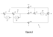
- Figure 2 shows a digital circuit 2 having the transfer function H(z) of equation [9], according to a second embodiment of the present invention.
- the digital circuit 2 comprises three delay lines D1', D2', D3', four adders A1', A2', A3', A4' and three multipliers M1', M2', M3'.
- a first adder A1' and a first delay line D1' are connected in a feedback configuration so as to form a first integrator I1'.
- a second adder A2' and a second delay line D2' are also connected in a feedback configuration so as to form a second integrator I2' cascaded with the first integrator I1'.
- the output of the first integrator I1' is connected to a first multiplier M1', which is configured to multiply its input by N-1.
- the output of the second delay line D2' is connected to a second multiplier M2', which is configured to multiply its input by 2.
- the output of the second integrator I2' is instead connected to third multiplier M3', which is configured to multiply its input by (N-1).
- Both the outputs of the first multiplier M1' and third multiplier M3' are connected to a third adder A3', whose output is in turn connected to a third delay line D3' suitable for delaying input values by N clock cycles.
- circuit of Figure 2 is instead advantageously even simpler than circuit 1, in that it comprises a reduced number of components (in particular, three delay lines instead of four delay lines).
- the digital circuit 2 according to the second embodiment is accordingly even simpler and less costly than circuit 1.
- Both the digital circuit 1 and the digital circuit 2 described herein after are suitable for calculating values of the slope ⁇ on a sliding window of N input digital samples, and for providing one value of the slope ⁇ at each clock cycle (namely, at each translation of the sliding window by one sample).
- all the elements operate at a same frequency f IN , which is the rate at which the sample values y k are fed to the circuit.
- decimation could be implemented by a down-sampler provided at the output of the circuit of Figure 2 and selecting one calculated value of the slope ⁇ every N calculated ones. This way, however, N-1 values every N ones would be needlessly calculated.
- the down-samplers M1', M2' and M3' select one input value every N ones (namely, every N clock cycles). This allows a reduction by a factor N of the operating frequency of the elements located downstream the down-samplers, namely the multipliers M1', M2', M3', the adders A3', A4' and the delay line D3'.
- the delay line D3' that, according to the second embodiment shown in Figure 2 , is configured to delay each received input value by N clock cycles (each clock cycle being 1/f IN ), according to such variant is replaced by a delay line D3" configured to delay each received input value by a single clock cycle, the clock cycle of the delay line D3" being now N/f IN .
- the circuit of Figure 3 is simpler than the circuit of Figure 2 with output down-sampler, the components located downstream the down-sampler being simpler than the corresponding ones in the non-decimated circuit.
- variants suitable for providing one value of the slope ⁇ every X ⁇ N clock cycles Similar considerations apply for variants suitable for providing one value of the slope ⁇ every X ⁇ N clock cycles.
- the delay line D3' delaying by N clock cycles is replaced by two simpler cascaded delay lines, one for delaying by 1 clock cycle and one for delaying by N-X clock cycles.
- the digital circuits according to embodiments of the present invention are advantageously much simpler than a FIR filter from a structural viewpoint. While indeed a FIR filter configured to implement slope filtering on N samples comprises N multipliers (or N/2, in case a folded structure is used), the above described circuits comprise a much lower number of multipliers, which moreover is independent of N. Such digital circuits have accordingly a very reduced cost and complexity, independently of the value of N. These features make the digital circuits of the present invention particularly advantageous for applications wherein slope filtering shall be performed on a particularly high number N of samples.
Landscapes
- Engineering & Computer Science (AREA)
- Physics & Mathematics (AREA)
- Mathematical Physics (AREA)
- Data Mining & Analysis (AREA)
- General Physics & Mathematics (AREA)
- Theoretical Computer Science (AREA)
- Pure & Applied Mathematics (AREA)
- Computational Mathematics (AREA)
- Mathematical Analysis (AREA)
- Mathematical Optimization (AREA)
- General Engineering & Computer Science (AREA)
- Databases & Information Systems (AREA)
- Software Systems (AREA)
- Algebra (AREA)
- Computer Hardware Design (AREA)
- Life Sciences & Earth Sciences (AREA)
- Bioinformatics & Cheminformatics (AREA)
- Bioinformatics & Computational Biology (AREA)
- Evolutionary Biology (AREA)
- Operations Research (AREA)
- Probability & Statistics with Applications (AREA)
- Complex Calculations (AREA)
Abstract

of N consecutive data samples y0, y1, ... yN-1. The digital circuit has a transfer function H(z) equal to a Z-transform of the above linear combination, divided by (1-z-1)2 and multiplied by (1-z-1)2. The transfer function H(z) in particular has a denominator (1-z-1)2 implemented by two cascaded integrators of the circuit, and a nominator that comprises a single multiplication by (N-1) implemented by a corresponding multiplier of the circuit. No other multipliers are required. The number of multipliers of the circuit is accordingly minimized and is independent of the number N. This makes the circuit simple, inexpensive and particularly suitable for noisy applications which require high values of N.
Description
- The present invention generally relates to the field of digital signal processing. More particularly, the present invention relates to a digital circuit for implementing a slope filtering on a sequence of equally spaced data samples, in particular data samples equally spaced in time.
- As it is known, given a set of data samples (x0, y0), (x1, y1), ... (xN-1, yN-1), a linear regression is a statistical operation consisting in calculating the best linear fit of such set of samples, namely in finding the straight line:

which better approximates the distribution of data samples. In equation [1], α is the y-intercept and β is the slope of the line. The y-intercept α and slope β are typically calculated using the least square method, that provides the following equations:
and
- In case the independent variable x is time, the slope β basically represents an average time derivative of the N data samples (x0, y0), (x1, y1), ... (xN-1, yN-1). Hence, assuming to acquire a theoretically infinite sequence of consecutive data samples, a time derivative of the data sample sequence may be estimated in real time by applying equation [3] to the N last acquired data samples, when a new sample is acquired. Such calculation will be termed herein after "slope filtering".
- Slope filtering has many applications, including digital communications where it is used e.g. for carrier recovery circuits to estimate the frequency offset and drift between clock oscillators of transmitter and receiver, in circuits for estimation of signal rate, signal transition and transition-polarity detection, in circuits for estimating chromatic dispersion in digital coherent receivers, and so on. Besides digital communications, slope filtering may be applied also to other scenarios, such as controllers for industrial processes (e.g. in PID controllers) and, more generally, to any scenario where a time derivative of samples continuously acquired in time at a certain rate shall be estimated in real time.
- "Slope filtering: FIR approach to linear regression" by Clay S. Turner, IEEE Signal Processing Magazine, November 2008, pages 159-163 discloses a time-domain slope filtering method which consists in calculating the slope β by means of a FIR filter. In particular, under the assumption that the data samples (x0, y0), (x1, y1) ... (xN-1, yN-1) are consecutive and equally spaced in time (namely if xK=x0+k with k=0, 1, 2, ... N-1, which is the case in most applications), equation [3] may be rewritten as:

where:
- The slope β therefore basically is a linear combination of the data sample values y0, y1, ... yN-1. Equation [4] may be accordingly implemented as a FIR (Finite Impulsive Response) filter with N stages, whose coefficients βk are provided by equation [5]. The coefficients βk provided by equation [5] form a ramp (namely, they vary linearly with k) and are symmetric relative to (N-1)/2, namely β0= - βN-1, β1= - βN-2, etc. Therefore, instead of a N-stage filter, a "folded" FIR filter with N/2 stages may be used.
- The inventors have noticed that use of a FIR filter for implementing slope filtering is disadvantageous in that such filter comprises a number of multipliers dependent from N, namely from the number of consecutive data samples which are taken into account for calculating each value of the slope β.
- Indeed, in most applications (in particular in digital communication applications) data samples are likely to be affected by a remarkable noise. In order to mitigate the detrimental effects of noise affecting single data samples onto the slope calculation, equation [4] shall be applied to a large number N of consecutive data samples. This however entails use of a FIR filter with a high number of multipliers, which is undesirable because multipliers represent the most complex and expensive elements of a digital circuit. Hence, in order to control the complexity and cost of a digital circuit, the number of multipliers which it comprises shall be minimized.
- In view of the above, the inventors have tackled the problem of providing a method and digital circuit for implementing a slope filtering on a sequence of equally spaced data samples, which overcomes the aforesaid drawback, namely wherein the number of multipliers is minimized and independent of the number N of consecutive data samples which are taken into account for calculating each value of the slope β.
- According to an aspect, there is provided a digital circuit for implementing a slope filtering on a sequence of data samples equally spaced in time, the slope filtering comprising calculating a linear combination according to the above equation [4] of N consecutive data samples (y0, y1, ... yN-1) of the sequence of data samples, wherein the digital circuit has a transfer function H(z) equal to the Z-transform HFIR(z) of the linear combination according to equation [4], divided by (1-z-1)2 and multiplied by (1-z-1)2.
- Preferably, the numerator of the transfer function H(z) comprises a multiplication by (N-1), the circuit comprising a first multiplier suitable for implementing the multiplication by (N-1).
- According to particularly preferred embodiments, (N-1) is a power of 2 and the first multiplier comprises a shift register.
- Preferably, the circuit further comprises a first integrator a second integrator cascaded with the first integrator, the first and second integrators being suitable for implementing two consecutive divisions by (1-z-1).
- According to a first embodiment, the digital circuit further comprises a circuit portion cascaded with the first and second integrators and having a transfer function corresponding to a numerator of the transfer function H(z).
- Preferably, such circuit portion comprises:
- a differentiator comprising a delay line and an adder connected in a feed-forward configuration, the differentiator being connected to an output of the second integrator;
- the first multiplier connected to an output of the differentiator;
- a second multiplier configured to multiply its input by 2 and connected to an output of the delay line of the differentiator;
- a third multiplier configured to multiply its input by 2 and connected to the output of the second integrator;
- a further adder connected to an output of the first multiplier and to an output of the third multiplier;
- a further delay line suitable for delaying its input by N clock cycles and connected to an output of the further adder; and
- a still further adder connected to an output of the further delay line, to the output of the first multiplier and to an output of the second multiplier.
- According to a second embodiment, the circuit further comprises:
- the first multiplier connected to an output of the first integrator;
- a second multiplier configured to multiply its input by 2 and connected to an output of a delay line of the second integrator;
- a third multiplier configured to multiply its input by 2 and connected to an output of the second integrator;
- an adder connected to an output of the first multiplier and to an output of the third multiplier;
- a further delay line suitable for delaying its input by N clock cycles and connected to an output of the further adder; and
- a still further adder connected to an output of the further delay line, to the output of the first multiplier and to an output of the second multiplier.
- Preferably, all components of the digital circuit are configured to operate at a same frequency fIN.
- According to a variant, the digital circuit further comprises at least one down-sampler located at an intermediate position of the circuit, the at least one down-sampler being configured to decimate its input thereby outputting a single value every X clock cycles, X being 1 < X ≤ N.
- Preferably, components of the circuit located upstream the at least one down-sampler are configured to operate at a first frequency fIN, and components of the circuit located downstream the at least one down-sampler are configured to operate at a second frequency lower than the first frequency fIN.
- Preferably, the circuit comprises adders and multipliers configured to implement modular arithmetic operations.
- The present invention will become clearer by reading the following detailed description, given by way of example and not of limitation, to be read by referring to the accompanying drawings, wherein:
-
Figure 1 shows a digital circuit according to a first embodiment of the present invention; -
Figure 2 shows a digital circuit according to a second embodiment of the present invention; and -
Figure 3 shows a digital circuit according to a variant of the second embodiment. - An N-stage FIR filter implementing the slope filtering calculation according to equation [4] using the coefficients βk provided by equation [5] has a transfer function equal to the Z-transform of equation [4], namely:

namely:
- Hence, βk = (N-1-2k), except the scaling factor

- It shall be noticed that, since - as mentioned above - the coefficients βk provided by equation [5] and rewritten in equation [7] are symmetric relative to (N-1)/2 (namely β0 = -βN-1, β1 = -βN-2, etc.), the FIR transfer function HFIR (z) has a zero at z=1 (namely, at ω=0).
- The inventors have noticed that, by multiplying and dividing the FIR transfer function HFIR(z) according to equation [7] by (1-z-1)2, the following transfer function H(z) is obtained:

- It can be noticed that the operation of multiplying HFIR(z) by (1-z-1)2 corresponds to applying a second derivative operation to the transfer function HFIR(z) and introduces a double zero of the transfer function H(z) at z=1.
- On the other hand, the operation of dividing HFIR(z) by (1-z-1)2 corresponds to applying a double integral to the transfer function HFIR(z) and introduces a double pole of the transfer function H(z) at z=1.
- Therefore, H(z) has a double pole at z=1 (due to double integral of HFIR(z)) and a triple zero at z=1 (namely, a zero of HFIR(z) and a double zero due to second derivative of HFIR(z)). This advantageously contributes to guarantee that a digital circuit having transfer function H(z) is functionally equivalent to a known FIR filter having transfer function HFIR(z), as it will be discussed in detail herein after.
- The numerator of equation [8] may also be rewritten as follows:

- It can be noticed that equation [9] comprises a particularly reduced number of multiplications, which is independent from N. In particular, such multiplications (which are all included in the numerator of equation [9]) comprise a multiplication by (N-1) and two multiplications by 2. Since, within the context of digital signal processing, a multiplication by 2 actually is a scaling which may be implemented by a shift register (and not by a multiplier), the transfer function H(z) of equation [9] may be implemented by a digital circuit which comprises a single multiplier by (N-1) (plus an optional multiplier by the scaling factor F, which is a constant factor and which accordingly may be merged in another circuit of the system in which slope calculation is implemented, e.g. in an ADC gain, a unit conversion factor, etc.), as it will be described in detail herein after.
-
Figure 1 shows adigital circuit 1 having the transfer function H(z) of equation [9], according to a first embodiment of the present invention. - The
digital circuit 1 comprises four delay lines D1, D2, D3, D4, five adders A1, A2, A3, A4, A5 and three multipliers M1, M2, M3. - A first adder A1 and a first delay line D1 (suitable for delaying input values by 1 clock cycle) are connected in a feedback configuration so as to form a first integrator I1. Similarly, a second adder A2 and a second delay line D2 (suitable for delaying input values by 1 clock cycle) are also connected in a feedback configuration so as to form a second integrator I2 cascaded with the first integrator I1.
- The other elements of the
digital circuit 1 are reciprocally interconnected so as to form an all-zero module M0 (namely, a module whose transfer function has only zeros and no poles) cascaded with the two integrators I1, I2. In particular, a third delay line D3 (suitable for delaying input values by 1 clock cycle) and a third adder A3 are connected in a feed-forward configuration, thereby forming a differentiator. The output of the third adder A3 is connected to a first multiplier M1, which is configured to multiply its input by (N-1). The output of the third delay line D3 is also connected to a second multiplier M2, which is configured to multiply its input by 2. The output of the second integrator I2 is also connected to a third multiplier M3, which is configured to multiply its input by 2. Both the outputs of the first multiplier M1 and third multiplier M3 are connected to a fourth adder A4. The output of the fourth adder A4 is in turn connected to a fourth delay line D4 suitable for delaying input values by N clock cycles. The outputs of the first multiplier M1, second multiplier M2 and fourth delay line D4 are connected to a fifth adder A5. It can be noticed that the transfer function of the all-zero module M0 is:
- Through simple algebraic steps, it can be easily derived that HM0(z) corresponds to the numerator of equation [9].
- Therefore, advantageously, the
digital circuit 1 implements slope filtering according to equation [9] through a very reduced number of multipliers. In particular, thedigital circuit 1 comprises only three multipliers: the multiplier M1 by (N-1) and two multipliers M2 and M3 by 2. As mentioned above, the multipliers M2 and M3 by 2 may be implemented as shift registers. Hence, thecircuit 1 actually comprises a single multiplier, namely M1. Moreover, if (N-1) is a power of 2, also the multiplier M1 may be implemented as a shift register. In such case, thedigital circuit 1 does not comprise any multiplier at all. Thedigital circuit 1 has accordingly a very reduced cost and complexity. - Moreover, the cost and complexity of the
circuit 1 is advantageously independent of N, namely of the number of consecutive data samples which are taken into account for calculating each value of the slope β. The number N may accordingly be set to very high values. Hence, thedigital circuit 1 implementing the slope filtering according to equation [9] is particularly advantageous for applications wherein data samples are affected by a relevant noise, whose detrimental effects on the slope filtering calculation shall be mitigated by performing the calculation on a large number N of consecutive data samples. - The
digital circuit 1 is advantageously equivalent to a FIR filter from every functional point of view. - In particular, although the
digital circuit 1 comprises two integrators I1, I2 at its input (which indefinitely cumulate the values y0, y1, ... yN-1 of the input data samples), similarly to a FIR filter the value of each sample affects the circuit output (namely, the calculated value of the slope β) for a finite number of clock cycles, namely N clock cycles. Therefore, in case of a sample affected by a particularly strong noise or in case of an anomalous event temporarily altering the value stored in one or more registers of thecircuit 1, the detrimental effect of this situation is automatically reset after expiration of a transient of N clock cycles. Similarly, the initial conditions of the registers of the circuit cease to produce their effects after N clock cycles. This is due to the fact that an anomalous value of an input sample or a register of thecircuit 1 basically can be seen as a constant added to the signal after the double integrator I1, I2. However, the double integrator I1, I2 is followed by the all-zero module M0 which has a triple zero in z=1, two zeros being cancelled by the two poles of the double integrator and the third one filtering out any constant component (ω=0) of the signal. - Furthermore, although it comprises two integrators I1, I2 at its input (which indefinitely cumulate the values of the input samples), the
digital circuit 1 may be designed so that it does not overflow. Indeed, assuming that the values y0, y1, ... yN-1 of the input data samples are comprised in the range [-1; 1], the output of the digital circuit 1 (namely the slope β) is limited as follows:
- Therefore, if Bin is the size in bits of the digitalized values y0, y1, ... yN-1 of the data samples at the input of the
circuit 1, the size in bits of the digitalized values of the slope β calculated at the output of thecircuit 1 is
- If the adders and multipliers of the
circuit 1 are design to implement modular arithmetic operations (namely, in two's complement format with Bout bits), when a multiplication or an addition is calculated, only the Bout least significant bits are considered, the exceeding ones being disregarded. This advantageously bounds the output of thecircuit 1 in the range [-2Bout-1; 2Bout-1 -1]. The error introduced by disregarding the exceeding bits in the integrators I1, I2 is cancelled by the differentiating operations implemented by the all-zero module M0. Also such differentiating operations are indeed modular, and therefore inherently eliminate possible spikes due to discontinuities affecting the sequence of values output by the integrators I1, I2 and being introduced by the modular operations performed by the adders A1, A2. -
Figure 2 shows adigital circuit 2 having the transfer function H(z) of equation [9], according to a second embodiment of the present invention. - The
digital circuit 2 comprises three delay lines D1', D2', D3', four adders A1', A2', A3', A4' and three multipliers M1', M2', M3'. - A first adder A1' and a first delay line D1' (suitable for delaying input values by 1 clock cycle) are connected in a feedback configuration so as to form a first integrator I1'. Similarly, a second adder A2' and a second delay line D2' (suitable for delaying input values by 1 clock cycle) are also connected in a feedback configuration so as to form a second integrator I2' cascaded with the first integrator I1'.
- The output of the first integrator I1' is connected to a first multiplier M1', which is configured to multiply its input by N-1. Besides, the output of the second delay line D2' is connected to a second multiplier M2', which is configured to multiply its input by 2. The output of the second integrator I2' is instead connected to third multiplier M3', which is configured to multiply its input by (N-1). Both the outputs of the first multiplier M1' and third multiplier M3' are connected to a third adder A3', whose output is in turn connected to a third delay line D3' suitable for delaying input values by N clock cycles. The outputs of the first multiplier M1', second multiplier M2' and third delay line D3' are connected to a fourth adder A4'. It can be noticed that the transfer function of
circuit 2 is as follows:
- Through simple algebraic steps, it can be easily derived that H'(z) corresponds to H(z) of equation [9]. Hence, the
circuit 2 ofFigure 2 is equivalent to thecircuit 1 ofFigure 1 from the functional point of view. The considerations about overflows and initial conditions discussed above with reference tocircuit 1 therefore apply also tocircuit 2. - From the structural point of view, the circuit of
Figure 2 is instead advantageously even simpler thancircuit 1, in that it comprises a reduced number of components (in particular, three delay lines instead of four delay lines). Thedigital circuit 2 according to the second embodiment is accordingly even simpler and less costly thancircuit 1. - Both the
digital circuit 1 and thedigital circuit 2 described herein after are suitable for calculating values of the slope β on a sliding window of N input digital samples, and for providing one value of the slope β at each clock cycle (namely, at each translation of the sliding window by one sample). Hence, in such circuits, all the elements operate at a same frequency fIN, which is the rate at which the sample values yk are fed to the circuit. - However, for some applications, it might be desirable providing only one value of the slope β every X clock cycles (1 < X ≤ N). This allows calculating the values of the slope β only for non-overlapping, contiguous time windows (X=N) or for time windows having a predefined overlap larger that a single sample (1<X<N).
-
Figure 3 shows a variant of the digital circuit ofFigure 2 , which provides a decimated output, in particular provides one value of the slope β every X=N clock cycles. - In principle, such decimation could be implemented by a down-sampler provided at the output of the circuit of
Figure 2 and selecting one calculated value of the slope β every N calculated ones. This way, however, N-1 values every N ones would be needlessly calculated. - According to the variant shown in
Figure 3 , instead of a single down-sampler at the output of the circuit, three down-samplers DS1, DS2 and DS3 are provided within thecircuit 2, in particular immediately before the multipliers M1', M2' and M3'. Therefore, suddenly after integrations carried out by the integrator I1' and/or I2', the down-samplers M1', M2' and M3' select one input value every N ones (namely, every N clock cycles). This allows a reduction by a factor N of the operating frequency of the elements located downstream the down-samplers, namely the multipliers M1', M2', M3', the adders A3', A4' and the delay line D3'. - Hence, while the integrators I1', I2' continue operating at the operating frequency fIN, the rest of the circuit advantageously operates at a must reduced frequency, namely fIN/N. In particular, the delay line D3' that, according to the second embodiment shown in
Figure 2 , is configured to delay each received input value by N clock cycles (each clock cycle being 1/fIN), according to such variant is replaced by a delay line D3" configured to delay each received input value by a single clock cycle, the clock cycle of the delay line D3" being now N/fIN. - Hence, according to such advantageous variant, the circuit of
Figure 3 is simpler than the circuit ofFigure 2 with output down-sampler, the components located downstream the down-sampler being simpler than the corresponding ones in the non-decimated circuit. - Similar considerations apply for variants suitable for providing one value of the slope β every X<N clock cycles. According to such variants, in particular, the delay line D3' delaying by N clock cycles is replaced by two simpler cascaded delay lines, one for delaying by 1 clock cycle and one for delaying by N-X clock cycles.
- Hence, while being functionally equivalent to a FIR filter suitable for implementing slope filtering, the digital circuits according to embodiments of the present invention are advantageously much simpler than a FIR filter from a structural viewpoint. While indeed a FIR filter configured to implement slope filtering on N samples comprises N multipliers (or N/2, in case a folded structure is used), the above described circuits comprise a much lower number of multipliers, which moreover is independent of N. Such digital circuits have accordingly a very reduced cost and complexity, independently of the value of N. These features make the digital circuits of the present invention particularly advantageous for applications wherein slope filtering shall be performed on a particularly high number N of samples.
Claims (11)
- A digital circuit (1; 2) for implementing a slope filtering on a sequence of data samples equally spaced in time, said slope filtering comprising calculating a linear combination:

- The digital circuit (1; 2) according to claim 1, wherein a numerator of said transfer function H(z) comprises a multiplication by (N-1), said circuit (1; 2) comprising a first multiplier (M1, M1') suitable for implementing said multiplication by (N-1).
- The digital circuit (1; 2) according to claim 2, wherein (N-1) is a power of 2 and said first multiplier (M1, M1') comprises a shift register.
- The digital circuit (1; 2) according to claim 2 or 3, wherein said circuit (1; 2) further comprises a first integrator (I1; I1') and a second integrator (I2; I2') cascaded with said first integrator (I1'; I1'), said first and second integrators (I1, I2; I1', I2') being suitable for implementing two consecutive divisions by (1-z-1).
- The digital circuit (1; 2) according to claim 4, wherein it further comprises a circuit portion (M0) cascaded with said first and second integrators (I1, I2) and having a transfer function corresponding to a numerator of said transfer function H(z).
- The digital circuit (1; 2) according to claim 5, wherein said circuit portion (M0) comprises:- a differentiator (D3, A3) comprising a delay line (D3) and an adder (A3) connected in a feed-forward configuration, said differentiator (D3, A3) being connected to an output of said second integrator (I2);- said first multiplier (M1) connected to an output of said differentiator (D3, A3);- a second multiplier (M2) configured to multiply its input by 2 and connected to an output of said delay line (D3);- a third multiplier (M3) configured to multiply its input by 2 and connected to said output of said second integrator (I2);- a further adder (A4) connected to an output of said first multiplier (M1) and to an output of said third multiplier (M3);- a further delay line (D4) suitable for delaying its input by N clock cycles and connected to an output of said further adder (A4); and- a still further adder (A5) connected to an output of said further delay line (D4), to said output of said first multiplier (M1) and to an output of said second multiplier (M2).
- The digital circuit (1; 2) according to claim 5, wherein said circuit (1; 2) further comprises:- said first multiplier (M1') connected to an output of said first integrator (I1');- a second multiplier (M2') configured to multiply its input by 2 and connected to an output of a delay line (D2') of said second integrator (I2');- a third multiplier (M3') configured to multiply its input by 2 and connected to an output of said second integrator (I2');- an adder (A3') connected to an output of said first multiplier (M1') and to an output of said third multiplier (M3');- a further delay line (D3') suitable for delaying its input by N clock cycles and connected to an output of said further adder (A3'); and- a still further adder (A4') connected to an output of said further delay line (D3'), to said output of said first multiplier (M1') and to an output of said second multiplier (M2').
- The digital circuit (1; 2) according to any of the preceding claims, wherein all components of said digital circuit (1; 2) are configured to operate at a same frequency fIN.
- The digital circuit (1; 2) according to any of claims 1 to 7, wherein it further comprises at least one down-sampler (DS1, DS2, DS3) located at an intermediate position of said circuit (1; 2), said at least one down-sampler (DS1, DS2, DS3) being configured to decimate its input thereby outputting a single value every X clock cycles, X being 1 < X ≤ N.
- The digital circuit (1; 2) according to claim 9, wherein components of said circuit (1; 2) located upstream said at least one down-sampler (DS1, DS2, DS3) are configured to operate at a first frequency fIN, and components of said circuit (1; 2) located downstream said at least one down-sampler (DS1, DS2, DS3) are configured to operate at a second frequency lower than said first frequency fIN.
- The digital circuit (1; 2) according to any of the preceding claims, wherein said circuit (1; 2) comprises adders and multipliers configured to implement modular arithmetic operations.
Priority Applications (1)
| Application Number | Priority Date | Filing Date | Title |
|---|---|---|---|
| EP13306313.1A EP2854043A1 (en) | 2013-09-26 | 2013-09-26 | Digital circuit for slope filtering |
Applications Claiming Priority (1)
| Application Number | Priority Date | Filing Date | Title |
|---|---|---|---|
| EP13306313.1A EP2854043A1 (en) | 2013-09-26 | 2013-09-26 | Digital circuit for slope filtering |
Publications (1)
| Publication Number | Publication Date |
|---|---|
| EP2854043A1 true EP2854043A1 (en) | 2015-04-01 |
Family
ID=49301409
Family Applications (1)
| Application Number | Title | Priority Date | Filing Date |
|---|---|---|---|
| EP13306313.1A Withdrawn EP2854043A1 (en) | 2013-09-26 | 2013-09-26 | Digital circuit for slope filtering |
Country Status (1)
| Country | Link |
|---|---|
| EP (1) | EP2854043A1 (en) |
Cited By (1)
| Publication number | Priority date | Publication date | Assignee | Title |
|---|---|---|---|---|
| CN119727664A (en) * | 2024-12-06 | 2025-03-28 | 西安交通大学 | A digital filter structure for Σ-Δ ADC downsampling |
-
2013
- 2013-09-26 EP EP13306313.1A patent/EP2854043A1/en not_active Withdrawn
Non-Patent Citations (6)
| Title |
|---|
| BROMBA M U A ET AL: "Efficient computation of polynomial smoothing digital filters", ANALYTICAL CHEMISTRY, vol. 51, no. 11, September 1979 (1979-09-01), pages 1760 - 1762, XP055133838, ISSN: 0003-2700, DOI: 10.1021/ac50047a038 * |
| CLAY S. TURNER: "Slope filtering: FIR approach to linear regression", IEEE SIGNAL PROCESSING MAGAZINE, November 2008 (2008-11-01), pages 159 - 163 |
| LYONS R G: "Understanding Digital Signal Processing - Third Edition", August 2012, PRENTICE HALL, pages: 820 - 821, XP055128413 * |
| MORGAN D R ET AL: "Nonuniform linear regression with block-wise sample-minimum preprocessing", IEEE TRANSACTIONS ON SIGNAL PROCESSING, vol. 58, no. 8, August 2010 (2010-08-01), pages 4040 - 4049, XP011307530, ISSN: 1053-587X * |
| SCOTT L B ET AL: "Efficient methods for data smoothing", SIAM JOURNAL OF NUMERICAL ANALYSIS, vol. 26, no. 3, June 1989 (1989-06-01), pages 681 - 692, XP008171140, ISSN: 0036-1429 * |
| TURNER C: "Slope filtering: An FIR approach to linear regression", IEEE SIGNAL PROCESSING MAGAZINE, vol. 25, no. 6, November 2008 (2008-11-01), pages 159 - 163, XP011236248, ISSN: 1053-5888, DOI: 10.1109/MSP.2008.929816 * |
Cited By (1)
| Publication number | Priority date | Publication date | Assignee | Title |
|---|---|---|---|---|
| CN119727664A (en) * | 2024-12-06 | 2025-03-28 | 西安交通大学 | A digital filter structure for Σ-Δ ADC downsampling |
Similar Documents
| Publication | Publication Date | Title |
|---|---|---|
| Laghari et al. | Performance analysis of analog butterworth low pass filter as compared to Chebyshev type-I filter, Chebyshev type-II filter and elliptical filter | |
| Fernandez-Vazquez et al. | Maximally flat CIC compensation filter: Design and multiplierless implementation | |
| US6721375B1 (en) | Method and device for compensating phase delays | |
| EP0373468B1 (en) | A pipelined processor for implementing the least-mean-squares algorithm | |
| Thakral et al. | Design and implementation of a high speed digital FIR filter using unfolding | |
| Dixit et al. | IIR filters using Xilinx System Generator for FPGA implementation | |
| EP2854043A1 (en) | Digital circuit for slope filtering | |
| CN114142830B (en) | FPGA Implementation of Full-precision Low-pass IIR Filter | |
| Bakshi et al. | Designand comparison between IIR Butterwoth and Chebyshev digital filters using Matlab | |
| US8645444B2 (en) | IIR filter for reducing the complexity of multiplying elements | |
| Abramovitch | The multinotch, part II: Extra precision via Δ coefficients | |
| CN103378821B (en) | Filter system | |
| EP3235147B1 (en) | Chromatic dispersion compensation filter | |
| Gunasekaran et al. | Low power and area efficient reconfigurable FIR filter implementation in FPGA | |
| US11057021B2 (en) | Fixed latency configurable tap digital filter | |
| Narasimha et al. | Implementation of low area and power efficient architectures for digital FIR filters | |
| Bharti et al. | Efficient design of different forms of FIR filter | |
| US7242326B1 (en) | Sample rate conversion combined with filter | |
| JP6410919B2 (en) | Phase frequency detector | |
| Chodoker et al. | Multiple Constant Multiplication Technique for Configurable Finite Impulse Response Filter Design | |
| Loganya et al. | Low Power VLSI Architecture for Reconfigurable FIR Filter | |
| Ali et al. | Multirate FIR filter using radix sort Booth algorithm in Xilinx System Generator | |
| Jovanović et al. | An approach to Digital Low-Pass IIR Filter Design | |
| Ahuja et al. | Design Of Efficient Add/Shift Algorithm For Multiple Constant Multiplication | |
| Khorbotly et al. | Recursive implementation of gaussian filters with switching and reset hardware |
Legal Events
| Date | Code | Title | Description |
|---|---|---|---|
| PUAI | Public reference made under article 153(3) epc to a published international application that has entered the european phase |
Free format text: ORIGINAL CODE: 0009012 |
|
| 17P | Request for examination filed |
Effective date: 20141218 |
|
| AK | Designated contracting states |
Kind code of ref document: A1 Designated state(s): AL AT BE BG CH CY CZ DE DK EE ES FI FR GB GR HR HU IE IS IT LI LT LU LV MC MK MT NL NO PL PT RO RS SE SI SK SM TR |
|
| AX | Request for extension of the european patent |
Extension state: BA ME |
|
| RBV | Designated contracting states (corrected) |
Designated state(s): AL AT BE BG CH CY CZ DE DK EE ES FI FR GB GR HR HU IE IS IT LI LT LU LV MC MK MT NL NO PL PT RO RS SE SI SK SM TR |
|
| RAP1 | Party data changed (applicant data changed or rights of an application transferred) |
Owner name: ALCATEL LUCENT |
|
| STAA | Information on the status of an ep patent application or granted ep patent |
Free format text: STATUS: THE APPLICATION IS DEEMED TO BE WITHDRAWN |
|
| 18D | Application deemed to be withdrawn |
Effective date: 20190402 |