EP2853449A1 - Electrical junction box - Google Patents
Electrical junction box Download PDFInfo
- Publication number
- EP2853449A1 EP2853449A1 EP14186843.0A EP14186843A EP2853449A1 EP 2853449 A1 EP2853449 A1 EP 2853449A1 EP 14186843 A EP14186843 A EP 14186843A EP 2853449 A1 EP2853449 A1 EP 2853449A1
- Authority
- EP
- European Patent Office
- Prior art keywords
- component mounting
- mounting section
- side component
- peripheral wall
- upper side
- Prior art date
- Legal status (The legal status is an assumption and is not a legal conclusion. Google has not performed a legal analysis and makes no representation as to the accuracy of the status listed.)
- Granted
Links
- 230000002093 peripheral effect Effects 0.000 claims abstract description 29
- 230000000694 effects Effects 0.000 description 1
- 230000004048 modification Effects 0.000 description 1
- 238000012986 modification Methods 0.000 description 1
Images


Classifications
-
- H—ELECTRICITY
- H02—GENERATION; CONVERSION OR DISTRIBUTION OF ELECTRIC POWER
- H02G—INSTALLATION OF ELECTRIC CABLES OR LINES, OR OF COMBINED OPTICAL AND ELECTRIC CABLES OR LINES
- H02G3/00—Installations of electric cables or lines or protective tubing therefor in or on buildings, equivalent structures or vehicles
- H02G3/02—Details
- H02G3/08—Distribution boxes; Connection or junction boxes
- H02G3/16—Distribution boxes; Connection or junction boxes structurally associated with support for line-connecting terminals within the box
-
- B—PERFORMING OPERATIONS; TRANSPORTING
- B60—VEHICLES IN GENERAL
- B60R—VEHICLES, VEHICLE FITTINGS, OR VEHICLE PARTS, NOT OTHERWISE PROVIDED FOR
- B60R16/00—Electric or fluid circuits specially adapted for vehicles and not otherwise provided for; Arrangement of elements of electric or fluid circuits specially adapted for vehicles and not otherwise provided for
- B60R16/02—Electric or fluid circuits specially adapted for vehicles and not otherwise provided for; Arrangement of elements of electric or fluid circuits specially adapted for vehicles and not otherwise provided for electric constitutive elements
- B60R16/023—Electric or fluid circuits specially adapted for vehicles and not otherwise provided for; Arrangement of elements of electric or fluid circuits specially adapted for vehicles and not otherwise provided for electric constitutive elements for transmission of signals between vehicle parts or subsystems
- B60R16/0238—Electrical distribution centers
-
- B—PERFORMING OPERATIONS; TRANSPORTING
- B60—VEHICLES IN GENERAL
- B60R—VEHICLES, VEHICLE FITTINGS, OR VEHICLE PARTS, NOT OTHERWISE PROVIDED FOR
- B60R16/00—Electric or fluid circuits specially adapted for vehicles and not otherwise provided for; Arrangement of elements of electric or fluid circuits specially adapted for vehicles and not otherwise provided for
- B60R16/02—Electric or fluid circuits specially adapted for vehicles and not otherwise provided for; Arrangement of elements of electric or fluid circuits specially adapted for vehicles and not otherwise provided for electric constitutive elements
- B60R16/023—Electric or fluid circuits specially adapted for vehicles and not otherwise provided for; Arrangement of elements of electric or fluid circuits specially adapted for vehicles and not otherwise provided for electric constitutive elements for transmission of signals between vehicle parts or subsystems
- B60R16/0239—Electronic boxes
Definitions
- This invention relates to electrical junction boxes mounted in automobiles for distributing electric power.
- Patent Literature 1 While there are various configurations for electrical junction box to be mounted in the automobile, for example, as disclosed in Patent Literature 1, well-known is an electrical junction box (1) having a frame-like case body (2), and a plurality of cassette blocks (3, 4) in which an electronic component is to be mounted, one of the cassette blocks (3) is attached to above in the case body (2), and the other cassette block (4) below the cassette block (3) in the case body (2).
- an electrical junction box (1) having a frame-like case body (2), and a plurality of cassette blocks (3, 4) in which an electronic component is to be mounted, one of the cassette blocks (3) is attached to above in the case body (2), and the other cassette block (4) below the cassette block (3) in the case body (2).
- the foregoing electrical junction box (1) and the cassette blocks (3,4) allow for an increase of the number of electronic components to be mounted without increasing a horizontal projected surface area. Also, when maintaining electronic component mounted to the lower step cassette block (4), removal of the upper side cassette block allows for maintaining the electronic component without removing the lower side cassette block (4) from the case body (2).
- the lower side cassette block (4) lies deep in the case body (2), in the case of an opening of the case body (2) being narrow, it is difficult to put an operator's hand or a tool within the case body (2), and to maintain the electronic component.
- the invention is intended to provide an electrical junction box provided with a frame including an upper side component mounting section and a lower side component mounting section, allowing for readily maintaining the electronic component mounted to the lower side component mounting section.
- the invention is related to an electrical junction box, including a frame including a peripheral wall, an upper side component mounting section located above in the peripheral wall, to which an electronic component is mounted, and a lower side component mounting section located below the upper side component mounting section in the peripheral wall, to which the electronic component is mounted, wherein a portion of the upper side component mounting section and a portion of the peripheral wall are integrally provided and are made attachable to a remaining portion of the frame, and wherein the lower side component mounting section is located below the portion of the upper side component mounting section.
- the portion of the upper side component mounting section and the portion of the peripheral wall are integrally provided and are made attachable to the remaining portion of the frame, and the lower side component mounting section is located below the portion of the upper side component mounting section, when maintaining the electronic component mounted to the lower side component mounting section, removal of a portion composed of the portion of the upper side component mounting section and the portion of the peripheral wall from the remaining portion of the frame eliminates a portion of the peripheral wall surrounding the lower side component mounting section, making it easy to put the operator's hand or the tool below in the peripheral wall. Therefore, it is made possible to readily maintain the electronic component mounted to the lower side component mounting section.
- An electrical junction box 1 shown in Fig. 1 is mounted to an automobile to chiefly distribute electric power.
- This electrical junction box 1 is provided with a synthetic-resin-made frame 2, a plurality of electronic components 10 to 13 to be attached to the frame 2, a synthetic-resin-made lower cover 3 to be attached to a lower face side of the frame 2, and a synthetic-resin-made upper cover (not shown) to be attached to an upper face side of the frame 2.
- the frame 2 is provided with a frame-like peripheral wall 20, an upper side component mounting section 21 located above in the peripheral wall 20, to which a plurality of electronic components 10, 11, 12 are to be mounted, and a lower side component mounting section 22 located below the upper side component mounting section 21 in the peripheral wall 20,to which a plurality of electronic components 13 are to be mounted. Also, the frame 2 is configured such that a plurality of blocks 5a, 5b, 5c, and 5d, a side cover 6, a divided section 7, and the like are assembled to a frame body 4 (corresponding to "a remaining portion of the frame” in claims) including a main portion of the peripheral wall 20.
- the foregoing blocks 5a, 5b, 5c are each provided with a plurality of component mounting sections to which electronic components 10, 11 is to be each mounted. These blocks 5a, 5b, 5c are assembled to within and above the frame body 4, so as to configure the upper side component mounting section 21. These blocks 5a, 5b, 5c do not include the peripheral wall 20.
- the upper side component mounting section 21 is defined as a whole of the plurality of component mounting sections disposed at the upper side of the frame 2.
- the plurality of blocks 5d is provided with a plurality of component mounting sections to be mounted to each electronic component 13.
- the plurality of blocks 5d is assembled to within and below the frame body 4 so as to compose the lower side component mounting section 22.
- the plurality of blocks 5d does not include the peripheral wall 20.
- the lower side component mounting section 22 is defined as a whole of the plurality of component mounting sections disposed at the lower side of the frame 2. Also, in the electrical junction box 1 two component mounting sections to which the relay 3 is mounted are disposed at each block 5d, the lower side component mounting section 22 is composed of three blocks 5d.
- the side cover 6 is located at a notch 23 formed at the peripheral wall 20.
- the foregoing divided section 7 is formed such that a portion 21a of the upper side component mounting section 21 and a portion 20a of the peripheral wall 20 are integrally provided.
- the portion 21a of the upper side component mounting section 21 includes three component mounting sections a connector 12 is attached to, and one component mounting section the relay 11 is mounted to.
- the portion 20a of the peripheral wall 20 is provided with two latch receiving parts 8. These latch receiving parts 8 is latched in a latch part 9 disposed at the frame 4.
- the divided section 7 is, when assembled to the frame body 4, secured to the frame 4 by latching the latch part 9 in the latch receiving part 8.
- the foregoing lower side component mounting section 22 is located below the divided section 7.
- the portion 21a of the upper side component mounting section 21 located above the lower side component mounting section 22 and the portion 20a of the peripheral wall 20 are thus divided as the divided section 7 from the frame body 4, when maintaining the relay 13 attached to the lower side component mounting section 22, removal of the divided section 7 from the frame body 4 allows for eliminating the portion 20a of the peripheral wall 20a surrounding the lower side component mounting section 22, making it easy to put the operator's hand or the tool downward in the peripheral wall 20. Thereby it is made easy to maintain the relay 13.
Landscapes
- Engineering & Computer Science (AREA)
- Mechanical Engineering (AREA)
- Architecture (AREA)
- Civil Engineering (AREA)
- Structural Engineering (AREA)
- Connection Or Junction Boxes (AREA)
Abstract
Description
- This application is on the basis of Japanese Patent Application
NO. 2013-204600 - This invention relates to electrical junction boxes mounted in automobiles for distributing electric power.
- While there are various configurations for electrical junction box to be mounted in the automobile, for example, as disclosed in
Patent Literature 1, well-known is an electrical junction box (1) having a frame-like case body (2), and a plurality of cassette blocks (3, 4) in which an electronic component is to be mounted, one of the cassette blocks (3) is attached to above in the case body (2), and the other cassette block (4) below the cassette block (3) in the case body (2). - By being stacked in vertical two steps, the foregoing electrical junction box (1) and the cassette blocks (3,4) allow for an increase of the number of electronic components to be mounted without increasing a horizontal projected surface area. Also, when maintaining electronic component mounted to the lower step cassette block (4), removal of the upper side cassette block allows for maintaining the electronic component without removing the lower side cassette block (4) from the case body (2).
- [PTL 1] Japanese Patent Application Laid-Open Publication No.
2011-10514 - Disadvantageously, since in the foregoing electrical junction box (1) of
PTL 1, although involving an advantage of maintaining the electronic component without removing the lower side cassette block (4) from the case body (2), the lower side cassette block (4) lies deep in the case body (2), in the case of an opening of the case body (2) being narrow, it is difficult to put an operator's hand or a tool within the case body (2), and to maintain the electronic component. - Accordingly, the invention is intended to provide an electrical junction box provided with a frame including an upper side component mounting section and a lower side component mounting section, allowing for readily maintaining the electronic component mounted to the lower side component mounting section.
- The invention according to one aspect is related to an electrical junction box, including a frame including a peripheral wall, an upper side component mounting section located above in the peripheral wall, to which an electronic component is mounted, and a lower side component mounting section located below the upper side component mounting section in the peripheral wall, to which the electronic component is mounted, wherein a portion of the upper side component mounting section and a portion of the peripheral wall are integrally provided and are made attachable to a remaining portion of the frame, and wherein the lower side component mounting section is located below the portion of the upper side component mounting section.
- According to the invention of the one aspect, since the portion of the upper side component mounting section and the portion of the peripheral wall are integrally provided and are made attachable to the remaining portion of the frame, and the lower side component mounting section is located below the portion of the upper side component mounting section, when maintaining the electronic component mounted to the lower side component mounting section, removal of a portion composed of the portion of the upper side component mounting section and the portion of the peripheral wall from the remaining portion of the frame eliminates a portion of the peripheral wall surrounding the lower side component mounting section, making it easy to put the operator's hand or the tool below in the peripheral wall. Therefore, it is made possible to readily maintain the electronic component mounted to the lower side component mounting section.
-
- [
Fig. 1 ]
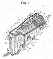
FIG. 1 is a perspective view illustrating an electrical junction box according to an embodiment of the invention; - [
Fig. 2 ]
FIG. 2 is a plane view illustrating the electrical junction box shown inFIG. 1 ; - [
Fig. 3 ]
FIG. 3 is a perspective view illustrating a state of removal of a divided section shown inFig. 1 from the frame body; and - [
Fig. 4 ]
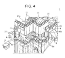
FIG. 4 is a perspective view illustrating a state of removal of a relay from the lower side component mounting section shown inFig. 3 . - Referring now to
Figs. 1 to 4 , "an electrical junction box" according to one embodiment of the invention will be discussed. Anelectrical junction box 1 shown inFig. 1 is mounted to an automobile to chiefly distribute electric power. Thiselectrical junction box 1 is provided with a synthetic-resin-madeframe 2, a plurality ofelectronic components 10 to 13 to be attached to theframe 2, a synthetic-resin-madelower cover 3 to be attached to a lower face side of theframe 2, and a synthetic-resin-made upper cover (not shown) to be attached to an upper face side of theframe 2. - The
frame 2 is provided with a frame-likeperipheral wall 20, an upper sidecomponent mounting section 21 located above in theperipheral wall 20, to which a plurality ofelectronic components component mounting section 22 located below the upper sidecomponent mounting section 21 in theperipheral wall 20,to which a plurality ofelectronic components 13 are to be mounted. Also, theframe 2 is configured such that a plurality ofblocks side cover 6, a dividedsection 7, and the like are assembled to a frame body 4 (corresponding to "a remaining portion of the frame" in claims) including a main portion of theperipheral wall 20. - The
foregoing blocks electronic components blocks frame body 4, so as to configure the upper sidecomponent mounting section 21. Theseblocks peripheral wall 20. In the invention "the upper sidecomponent mounting section 21" is defined as a whole of the plurality of component mounting sections disposed at the upper side of theframe 2. - The plurality of
blocks 5d is provided with a plurality of component mounting sections to be mounted to eachelectronic component 13. The plurality ofblocks 5d is assembled to within and below theframe body 4 so as to compose the lower sidecomponent mounting section 22. The plurality ofblocks 5d does not include theperipheral wall 20. In the invention "the lower sidecomponent mounting section 22" is defined as a whole of the plurality of component mounting sections disposed at the lower side of theframe 2. Also, in theelectrical junction box 1 two component mounting sections to which therelay 3 is mounted are disposed at eachblock 5d, the lower sidecomponent mounting section 22 is composed of threeblocks 5d. - The
side cover 6 is located at anotch 23 formed at theperipheral wall 20. - The foregoing divided
section 7 is formed such that aportion 21a of the upper sidecomponent mounting section 21 and aportion 20a of theperipheral wall 20 are integrally provided. As shown inFig. 2 , in theelectrical junction box 1 theportion 21a of the upper sidecomponent mounting section 21 includes three component mounting sections aconnector 12 is attached to, and one component mounting section therelay 11 is mounted to. Theportion 20a of theperipheral wall 20 is provided with twolatch receiving parts 8. Theselatch receiving parts 8 is latched in alatch part 9 disposed at theframe 4. The dividedsection 7 is, when assembled to theframe body 4, secured to theframe 4 by latching thelatch part 9 in thelatch receiving part 8. The foregoing lower sidecomponent mounting section 22 is located below the dividedsection 7. - In the
electrical junction box 1 configured as mentioned above, when changing therelay 13 mounted to the lower sidecomponent mounting section 22, as shown inFigs. 3 and4 , unlatching of thelatch receiving part 8 and thelatch part 9, removing of theframe body 4 from the dividedsection 7 and lifting upward of the divided section 7 (because an electric wire is drawn from a lower face of the divided section 7) perform changing of therelay 3. - Since in the
electrical junction box 1 theportion 21a of the upper sidecomponent mounting section 21 located above the lower sidecomponent mounting section 22 and theportion 20a of theperipheral wall 20 are thus divided as the dividedsection 7 from theframe body 4, when maintaining therelay 13 attached to the lower sidecomponent mounting section 22, removal of the dividedsection 7 from theframe body 4 allows for eliminating theportion 20a of theperipheral wall 20a surrounding the lower sidecomponent mounting section 22, making it easy to put the operator's hand or the tool downward in theperipheral wall 20. Thereby it is made easy to maintain therelay 13. - Note that the aforementioned embodiments merely typically discloses the present invention, and are not intended to limit the invention. Namely, unless such changes and modifications depart from the scope of the present invention, they should be construed as being included therein.
- 1
- 1
- electrical junction box
- 2
- frame
- 4
- frame body
- 7
- divided section
- 20
- peripheral wall
- 21
- upper side component mounting section
- 22
- lower side component mounting section
Claims (1)
- An electrical junction box, comprising:a frame includinga peripheral wall,an upper side component mounting section located above in the peripheral wall, and having an electronic component mounted thereto, anda lower side component mounting section located below the upper side component mounting section in the peripheral wall, and having the electronic component mounted thereto,wherein a portion of the upper side component mounting section anda portion of the peripheral wall are integrally provided and are made attachable to a remaining portion of the frame, andwherein the lower side component mounting section is located below the portion of the upper side component mounting section.
Applications Claiming Priority (1)
| Application Number | Priority Date | Filing Date | Title |
|---|---|---|---|
| JP2013204600A JP6045075B2 (en) | 2013-09-30 | 2013-09-30 | Electrical junction box |
Publications (2)
| Publication Number | Publication Date |
|---|---|
| EP2853449A1 true EP2853449A1 (en) | 2015-04-01 |
| EP2853449B1 EP2853449B1 (en) | 2015-10-28 |
Family
ID=51619100
Family Applications (1)
| Application Number | Title | Priority Date | Filing Date |
|---|---|---|---|
| EP14186843.0A Active EP2853449B1 (en) | 2013-09-30 | 2014-09-29 | Electrical junction box |
Country Status (4)
| Country | Link |
|---|---|
| US (1) | US20150092384A1 (en) |
| EP (1) | EP2853449B1 (en) |
| JP (1) | JP6045075B2 (en) |
| CN (1) | CN104518464A (en) |
Families Citing this family (5)
| Publication number | Priority date | Publication date | Assignee | Title |
|---|---|---|---|---|
| JP5875154B2 (en) * | 2012-07-25 | 2016-03-02 | 矢崎総業株式会社 | Electrical junction box |
| JP6473470B2 (en) * | 2017-03-09 | 2019-02-20 | 矢崎総業株式会社 | Electrical junction box and wire harness |
| JP6582016B2 (en) * | 2017-05-23 | 2019-09-25 | 矢崎総業株式会社 | Electrical junction box |
| JP6919599B2 (en) * | 2018-03-05 | 2021-08-18 | 住友電装株式会社 | Electrical junction box |
| JP7513661B2 (en) * | 2022-07-06 | 2024-07-09 | 矢崎総業株式会社 | Electrical Junction Box |
Citations (4)
| Publication number | Priority date | Publication date | Assignee | Title |
|---|---|---|---|---|
| EP0497198B1 (en) * | 1991-01-29 | 1995-12-27 | VDO Adolf Schindling AG | Rectangular parallelepiped housing for an electronic device with plug connections |
| US5777843A (en) * | 1996-07-12 | 1998-07-07 | Yazaki Corporation | Power distribution box and housing assembly |
| JP2011010514A (en) | 2009-06-29 | 2011-01-13 | Yazaki Corp | Electrical connection box |
| JP2013204600A (en) | 2012-03-27 | 2013-10-07 | Jvc Kenwood Corp | Holder holding structure and portable apparatus having the same |
Family Cites Families (10)
| Publication number | Priority date | Publication date | Assignee | Title |
|---|---|---|---|---|
| US5207587A (en) * | 1992-05-27 | 1993-05-04 | General Motors Corporation | Electrical distribution center |
| US5788529A (en) * | 1997-06-09 | 1998-08-04 | General Motors Corporation | Top down electrical distribution center assembly |
| US5971796A (en) * | 1998-06-02 | 1999-10-26 | Yazaki Corporation | Wire harness and connector shroud |
| JP2006320147A (en) * | 2005-05-13 | 2006-11-24 | Yazaki Corp | Electrical junction box |
| JP4714569B2 (en) * | 2005-11-22 | 2011-06-29 | 矢崎総業株式会社 | Electrical junction box |
| JP2007288975A (en) * | 2006-04-19 | 2007-11-01 | Yazaki Corp | Electrical junction box |
| JP4605112B2 (en) * | 2006-07-18 | 2011-01-05 | 住友電装株式会社 | Electrical junction box |
| JP5088090B2 (en) * | 2007-10-26 | 2012-12-05 | 住友電装株式会社 | In-vehicle electrical junction box |
| JP5067199B2 (en) * | 2008-02-29 | 2012-11-07 | 住友電装株式会社 | In-vehicle electrical junction box |
| JP5612987B2 (en) * | 2010-09-29 | 2014-10-22 | 矢崎総業株式会社 | Electrical junction box |
-
2013
- 2013-09-30 JP JP2013204600A patent/JP6045075B2/en active Active
-
2014
- 2014-09-29 EP EP14186843.0A patent/EP2853449B1/en active Active
- 2014-09-30 CN CN201410521132.9A patent/CN104518464A/en active Pending
- 2014-09-30 US US14/501,527 patent/US20150092384A1/en not_active Abandoned
Patent Citations (4)
| Publication number | Priority date | Publication date | Assignee | Title |
|---|---|---|---|---|
| EP0497198B1 (en) * | 1991-01-29 | 1995-12-27 | VDO Adolf Schindling AG | Rectangular parallelepiped housing for an electronic device with plug connections |
| US5777843A (en) * | 1996-07-12 | 1998-07-07 | Yazaki Corporation | Power distribution box and housing assembly |
| JP2011010514A (en) | 2009-06-29 | 2011-01-13 | Yazaki Corp | Electrical connection box |
| JP2013204600A (en) | 2012-03-27 | 2013-10-07 | Jvc Kenwood Corp | Holder holding structure and portable apparatus having the same |
Also Published As
| Publication number | Publication date |
|---|---|
| CN104518464A (en) | 2015-04-15 |
| JP6045075B2 (en) | 2016-12-14 |
| JP2015070733A (en) | 2015-04-13 |
| US20150092384A1 (en) | 2015-04-02 |
| EP2853449B1 (en) | 2015-10-28 |
Similar Documents
| Publication | Publication Date | Title |
|---|---|---|
| EP2853449B1 (en) | Electrical junction box | |
| CN106535519B (en) | Electrical equipment housing and power conversion device | |
| US20190013654A1 (en) | Wire housing protector | |
| JP6581950B2 (en) | Fuse box | |
| JP2016185023A (en) | Protector and wiring module with protector | |
| US8881928B2 (en) | Casing cover | |
| CN103887747B (en) | Electrical junction box | |
| CN104659721B (en) | Electric circuit connection container | |
| CN104795776B (en) | Electrical junction box | |
| US20140131089A1 (en) | Electrical junction box | |
| JP2012224267A (en) | Electrical component mounting board | |
| JP6103387B2 (en) | Protective case | |
| JP2014236656A (en) | Electric connection box | |
| EP2876802B1 (en) | Inverter device | |
| JP2011239557A (en) | Electrical connection box | |
| JP6546421B2 (en) | Electrical connection box and wire harness | |
| JP6253542B2 (en) | Equipment fixing member | |
| JP2016025738A (en) | Electric connection box | |
| JP6355524B2 (en) | Switch terminal cover | |
| JP5932729B2 (en) | Energy measuring device | |
| JP6262100B2 (en) | Electrical junction box | |
| JP5906979B2 (en) | Electrical junction box | |
| JP6386721B2 (en) | Electrical junction box | |
| WO2015033903A1 (en) | Electrical junction box | |
| JP2013074682A (en) | Electric connection box |
Legal Events
| Date | Code | Title | Description |
|---|---|---|---|
| PUAI | Public reference made under article 153(3) epc to a published international application that has entered the european phase |
Free format text: ORIGINAL CODE: 0009012 |
|
| 17P | Request for examination filed |
Effective date: 20140929 |
|
| AK | Designated contracting states |
Kind code of ref document: A1 Designated state(s): AL AT BE BG CH CY CZ DE DK EE ES FI FR GB GR HR HU IE IS IT LI LT LU LV MC MK MT NL NO PL PT RO RS SE SI SK SM TR |
|
| AX | Request for extension of the european patent |
Extension state: BA ME |
|
| GRAP | Despatch of communication of intention to grant a patent |
Free format text: ORIGINAL CODE: EPIDOSNIGR1 |
|
| R17P | Request for examination filed (corrected) |
Effective date: 20150515 |
|
| RBV | Designated contracting states (corrected) |
Designated state(s): AL AT BE BG CH CY CZ DE DK EE ES FI FR GB GR HR HU IE IS IT LI LT LU LV MC MK MT NL NO PL PT RO RS SE SI SK SM TR |
|
| INTG | Intention to grant announced |
Effective date: 20150623 |
|
| GRAS | Grant fee paid |
Free format text: ORIGINAL CODE: EPIDOSNIGR3 |
|
| GRAA | (expected) grant |
Free format text: ORIGINAL CODE: 0009210 |
|
| AK | Designated contracting states |
Kind code of ref document: B1 Designated state(s): AL AT BE BG CH CY CZ DE DK EE ES FI FR GB GR HR HU IE IS IT LI LT LU LV MC MK MT NL NO PL PT RO RS SE SI SK SM TR |
|
| REG | Reference to a national code |
Ref country code: GB Ref legal event code: FG4D |
|
| REG | Reference to a national code |
Ref country code: CH Ref legal event code: EP |
|
| REG | Reference to a national code |
Ref country code: AT Ref legal event code: REF Ref document number: 757745 Country of ref document: AT Kind code of ref document: T Effective date: 20151115 |
|
| REG | Reference to a national code |
Ref country code: IE Ref legal event code: FG4D |
|
| REG | Reference to a national code |
Ref country code: DE Ref legal event code: R096 Ref document number: 602014000390 Country of ref document: DE |
|
| REG | Reference to a national code |
Ref country code: LT Ref legal event code: MG4D |
|
| REG | Reference to a national code |
Ref country code: NL Ref legal event code: MP Effective date: 20151028 |
|
| REG | Reference to a national code |
Ref country code: AT Ref legal event code: MK05 Ref document number: 757745 Country of ref document: AT Kind code of ref document: T Effective date: 20151028 |
|
| PG25 | Lapsed in a contracting state [announced via postgrant information from national office to epo] |
Ref country code: LT Free format text: LAPSE BECAUSE OF FAILURE TO SUBMIT A TRANSLATION OF THE DESCRIPTION OR TO PAY THE FEE WITHIN THE PRESCRIBED TIME-LIMIT Effective date: 20151028 Ref country code: ES Free format text: LAPSE BECAUSE OF FAILURE TO SUBMIT A TRANSLATION OF THE DESCRIPTION OR TO PAY THE FEE WITHIN THE PRESCRIBED TIME-LIMIT Effective date: 20151028 Ref country code: IS Free format text: LAPSE BECAUSE OF FAILURE TO SUBMIT A TRANSLATION OF THE DESCRIPTION OR TO PAY THE FEE WITHIN THE PRESCRIBED TIME-LIMIT Effective date: 20160228 Ref country code: HR Free format text: LAPSE BECAUSE OF FAILURE TO SUBMIT A TRANSLATION OF THE DESCRIPTION OR TO PAY THE FEE WITHIN THE PRESCRIBED TIME-LIMIT Effective date: 20151028 Ref country code: NL Free format text: LAPSE BECAUSE OF FAILURE TO SUBMIT A TRANSLATION OF THE DESCRIPTION OR TO PAY THE FEE WITHIN THE PRESCRIBED TIME-LIMIT Effective date: 20151028 Ref country code: IT Free format text: LAPSE BECAUSE OF FAILURE TO SUBMIT A TRANSLATION OF THE DESCRIPTION OR TO PAY THE FEE WITHIN THE PRESCRIBED TIME-LIMIT Effective date: 20151028 Ref country code: NO Free format text: LAPSE BECAUSE OF FAILURE TO SUBMIT A TRANSLATION OF THE DESCRIPTION OR TO PAY THE FEE WITHIN THE PRESCRIBED TIME-LIMIT Effective date: 20160128 |
|
| PG25 | Lapsed in a contracting state [announced via postgrant information from national office to epo] |
Ref country code: SE Free format text: LAPSE BECAUSE OF FAILURE TO SUBMIT A TRANSLATION OF THE DESCRIPTION OR TO PAY THE FEE WITHIN THE PRESCRIBED TIME-LIMIT Effective date: 20151028 Ref country code: FI Free format text: LAPSE BECAUSE OF FAILURE TO SUBMIT A TRANSLATION OF THE DESCRIPTION OR TO PAY THE FEE WITHIN THE PRESCRIBED TIME-LIMIT Effective date: 20151028 Ref country code: PT Free format text: LAPSE BECAUSE OF FAILURE TO SUBMIT A TRANSLATION OF THE DESCRIPTION OR TO PAY THE FEE WITHIN THE PRESCRIBED TIME-LIMIT Effective date: 20160229 Ref country code: LV Free format text: LAPSE BECAUSE OF FAILURE TO SUBMIT A TRANSLATION OF THE DESCRIPTION OR TO PAY THE FEE WITHIN THE PRESCRIBED TIME-LIMIT Effective date: 20151028 Ref country code: GR Free format text: LAPSE BECAUSE OF FAILURE TO SUBMIT A TRANSLATION OF THE DESCRIPTION OR TO PAY THE FEE WITHIN THE PRESCRIBED TIME-LIMIT Effective date: 20160129 Ref country code: RS Free format text: LAPSE BECAUSE OF FAILURE TO SUBMIT A TRANSLATION OF THE DESCRIPTION OR TO PAY THE FEE WITHIN THE PRESCRIBED TIME-LIMIT Effective date: 20151028 Ref country code: AT Free format text: LAPSE BECAUSE OF FAILURE TO SUBMIT A TRANSLATION OF THE DESCRIPTION OR TO PAY THE FEE WITHIN THE PRESCRIBED TIME-LIMIT Effective date: 20151028 Ref country code: PL Free format text: LAPSE BECAUSE OF FAILURE TO SUBMIT A TRANSLATION OF THE DESCRIPTION OR TO PAY THE FEE WITHIN THE PRESCRIBED TIME-LIMIT Effective date: 20151028 |
|
| PG25 | Lapsed in a contracting state [announced via postgrant information from national office to epo] |
Ref country code: CZ Free format text: LAPSE BECAUSE OF FAILURE TO SUBMIT A TRANSLATION OF THE DESCRIPTION OR TO PAY THE FEE WITHIN THE PRESCRIBED TIME-LIMIT Effective date: 20151028 |
|
| REG | Reference to a national code |
Ref country code: DE Ref legal event code: R097 Ref document number: 602014000390 Country of ref document: DE |
|
| PG25 | Lapsed in a contracting state [announced via postgrant information from national office to epo] |
Ref country code: SM Free format text: LAPSE BECAUSE OF FAILURE TO SUBMIT A TRANSLATION OF THE DESCRIPTION OR TO PAY THE FEE WITHIN THE PRESCRIBED TIME-LIMIT Effective date: 20151028 Ref country code: DK Free format text: LAPSE BECAUSE OF FAILURE TO SUBMIT A TRANSLATION OF THE DESCRIPTION OR TO PAY THE FEE WITHIN THE PRESCRIBED TIME-LIMIT Effective date: 20151028 Ref country code: RO Free format text: LAPSE BECAUSE OF FAILURE TO SUBMIT A TRANSLATION OF THE DESCRIPTION OR TO PAY THE FEE WITHIN THE PRESCRIBED TIME-LIMIT Effective date: 20151028 Ref country code: SK Free format text: LAPSE BECAUSE OF FAILURE TO SUBMIT A TRANSLATION OF THE DESCRIPTION OR TO PAY THE FEE WITHIN THE PRESCRIBED TIME-LIMIT Effective date: 20151028 Ref country code: EE Free format text: LAPSE BECAUSE OF FAILURE TO SUBMIT A TRANSLATION OF THE DESCRIPTION OR TO PAY THE FEE WITHIN THE PRESCRIBED TIME-LIMIT Effective date: 20151028 |
|
| PLBE | No opposition filed within time limit |
Free format text: ORIGINAL CODE: 0009261 |
|
| STAA | Information on the status of an ep patent application or granted ep patent |
Free format text: STATUS: NO OPPOSITION FILED WITHIN TIME LIMIT |
|
| 26N | No opposition filed |
Effective date: 20160729 |
|
| PG25 | Lapsed in a contracting state [announced via postgrant information from national office to epo] |
Ref country code: SI Free format text: LAPSE BECAUSE OF FAILURE TO SUBMIT A TRANSLATION OF THE DESCRIPTION OR TO PAY THE FEE WITHIN THE PRESCRIBED TIME-LIMIT Effective date: 20151028 |
|
| PG25 | Lapsed in a contracting state [announced via postgrant information from national office to epo] |
Ref country code: BE Free format text: LAPSE BECAUSE OF FAILURE TO SUBMIT A TRANSLATION OF THE DESCRIPTION OR TO PAY THE FEE WITHIN THE PRESCRIBED TIME-LIMIT Effective date: 20151028 |
|
| PG25 | Lapsed in a contracting state [announced via postgrant information from national office to epo] |
Ref country code: MC Free format text: LAPSE BECAUSE OF FAILURE TO SUBMIT A TRANSLATION OF THE DESCRIPTION OR TO PAY THE FEE WITHIN THE PRESCRIBED TIME-LIMIT Effective date: 20151028 |
|
| REG | Reference to a national code |
Ref country code: IE Ref legal event code: MM4A |
|
| REG | Reference to a national code |
Ref country code: FR Ref legal event code: ST Effective date: 20170531 |
|
| PG25 | Lapsed in a contracting state [announced via postgrant information from national office to epo] |
Ref country code: FR Free format text: LAPSE BECAUSE OF NON-PAYMENT OF DUE FEES Effective date: 20160930 Ref country code: IE Free format text: LAPSE BECAUSE OF NON-PAYMENT OF DUE FEES Effective date: 20160929 |
|
| PG25 | Lapsed in a contracting state [announced via postgrant information from national office to epo] |
Ref country code: LU Free format text: LAPSE BECAUSE OF NON-PAYMENT OF DUE FEES Effective date: 20160929 |
|
| REG | Reference to a national code |
Ref country code: CH Ref legal event code: PL |
|
| PG25 | Lapsed in a contracting state [announced via postgrant information from national office to epo] |
Ref country code: HU Free format text: LAPSE BECAUSE OF FAILURE TO SUBMIT A TRANSLATION OF THE DESCRIPTION OR TO PAY THE FEE WITHIN THE PRESCRIBED TIME-LIMIT; INVALID AB INITIO Effective date: 20140929 |
|
| PG25 | Lapsed in a contracting state [announced via postgrant information from national office to epo] |
Ref country code: MK Free format text: LAPSE BECAUSE OF FAILURE TO SUBMIT A TRANSLATION OF THE DESCRIPTION OR TO PAY THE FEE WITHIN THE PRESCRIBED TIME-LIMIT Effective date: 20151028 Ref country code: CY Free format text: LAPSE BECAUSE OF FAILURE TO SUBMIT A TRANSLATION OF THE DESCRIPTION OR TO PAY THE FEE WITHIN THE PRESCRIBED TIME-LIMIT Effective date: 20151028 Ref country code: MT Free format text: LAPSE BECAUSE OF NON-PAYMENT OF DUE FEES Effective date: 20160930 |
|
| PG25 | Lapsed in a contracting state [announced via postgrant information from national office to epo] |
Ref country code: BG Free format text: LAPSE BECAUSE OF FAILURE TO SUBMIT A TRANSLATION OF THE DESCRIPTION OR TO PAY THE FEE WITHIN THE PRESCRIBED TIME-LIMIT Effective date: 20151028 Ref country code: CH Free format text: LAPSE BECAUSE OF NON-PAYMENT OF DUE FEES Effective date: 20170930 Ref country code: LI Free format text: LAPSE BECAUSE OF NON-PAYMENT OF DUE FEES Effective date: 20170930 |
|
| PG25 | Lapsed in a contracting state [announced via postgrant information from national office to epo] |
Ref country code: TR Free format text: LAPSE BECAUSE OF FAILURE TO SUBMIT A TRANSLATION OF THE DESCRIPTION OR TO PAY THE FEE WITHIN THE PRESCRIBED TIME-LIMIT Effective date: 20151028 Ref country code: AL Free format text: LAPSE BECAUSE OF FAILURE TO SUBMIT A TRANSLATION OF THE DESCRIPTION OR TO PAY THE FEE WITHIN THE PRESCRIBED TIME-LIMIT Effective date: 20151028 |
|
| GBPC | Gb: european patent ceased through non-payment of renewal fee |
Effective date: 20180929 |
|
| PG25 | Lapsed in a contracting state [announced via postgrant information from national office to epo] |
Ref country code: GB Free format text: LAPSE BECAUSE OF NON-PAYMENT OF DUE FEES Effective date: 20180929 |
|
| PGFP | Annual fee paid to national office [announced via postgrant information from national office to epo] |
Ref country code: DE Payment date: 20240806 Year of fee payment: 11 |