EP2851740A1 - Optical element, and photodetector - Google Patents
Optical element, and photodetector Download PDFInfo
- Publication number
- EP2851740A1 EP2851740A1 EP13791691.2A EP13791691A EP2851740A1 EP 2851740 A1 EP2851740 A1 EP 2851740A1 EP 13791691 A EP13791691 A EP 13791691A EP 2851740 A1 EP2851740 A1 EP 2851740A1
- Authority
- EP
- European Patent Office
- Prior art keywords
- optical element
- predetermined direction
- region
- light
- photodetector
- Prior art date
- Legal status (The legal status is an assumption and is not a legal conclusion. Google has not performed a legal analysis and makes no representation as to the accuracy of the status listed.)
- Withdrawn
Links
- 230000003287 optical effect Effects 0.000 title claims abstract description 148
- 230000005684 electric field Effects 0.000 claims description 78
- 239000004065 semiconductor Substances 0.000 claims description 56
- 230000000149 penetrating effect Effects 0.000 claims description 8
- 239000000758 substrate Substances 0.000 claims description 8
- 239000000463 material Substances 0.000 description 19
- 238000000034 method Methods 0.000 description 11
- 229910052732 germanium Inorganic materials 0.000 description 8
- GNPVGFCGXDBREM-UHFFFAOYSA-N germanium atom Chemical compound [Ge] GNPVGFCGXDBREM-UHFFFAOYSA-N 0.000 description 8
- 238000006243 chemical reaction Methods 0.000 description 6
- 239000003574 free electron Substances 0.000 description 5
- 206010034972 Photosensitivity reaction Diseases 0.000 description 4
- VYPSYNLAJGMNEJ-UHFFFAOYSA-N Silicium dioxide Chemical compound O=[Si]=O VYPSYNLAJGMNEJ-UHFFFAOYSA-N 0.000 description 4
- 238000004364 calculation method Methods 0.000 description 4
- 230000000694 effects Effects 0.000 description 4
- 239000010931 gold Substances 0.000 description 4
- 229910052751 metal Inorganic materials 0.000 description 4
- 239000002184 metal Substances 0.000 description 4
- 230000036211 photosensitivity Effects 0.000 description 4
- 238000004088 simulation Methods 0.000 description 4
- PCHJSUWPFVWCPO-UHFFFAOYSA-N gold Chemical compound [Au] PCHJSUWPFVWCPO-UHFFFAOYSA-N 0.000 description 3
- 229910052737 gold Inorganic materials 0.000 description 3
- 230000007704 transition Effects 0.000 description 3
- 229910000530 Gallium indium arsenide Inorganic materials 0.000 description 2
- 230000008859 change Effects 0.000 description 2
- 238000010276 construction Methods 0.000 description 2
- 230000001747 exhibiting effect Effects 0.000 description 2
- 230000031700 light absorption Effects 0.000 description 2
- 238000004519 manufacturing process Methods 0.000 description 2
- 230000000737 periodic effect Effects 0.000 description 2
- 230000002093 peripheral effect Effects 0.000 description 2
- 235000012239 silicon dioxide Nutrition 0.000 description 2
- 239000000377 silicon dioxide Substances 0.000 description 2
- 238000001228 spectrum Methods 0.000 description 2
- 229910052581 Si3N4 Inorganic materials 0.000 description 1
- XUIMIQQOPSSXEZ-UHFFFAOYSA-N Silicon Chemical compound [Si] XUIMIQQOPSSXEZ-UHFFFAOYSA-N 0.000 description 1
- 230000009471 action Effects 0.000 description 1
- 230000001154 acute effect Effects 0.000 description 1
- 239000000470 constituent Substances 0.000 description 1
- 230000002542 deteriorative effect Effects 0.000 description 1
- 230000002708 enhancing effect Effects 0.000 description 1
- 239000010419 fine particle Substances 0.000 description 1
- 150000002739 metals Chemical class 0.000 description 1
- TWNQGVIAIRXVLR-UHFFFAOYSA-N oxo(oxoalumanyloxy)alumane Chemical compound O=[Al]O[Al]=O TWNQGVIAIRXVLR-UHFFFAOYSA-N 0.000 description 1
- 230000035699 permeability Effects 0.000 description 1
- 230000010287 polarization Effects 0.000 description 1
- 230000008569 process Effects 0.000 description 1
- 230000001902 propagating effect Effects 0.000 description 1
- 239000002096 quantum dot Substances 0.000 description 1
- 230000035945 sensitivity Effects 0.000 description 1
- 229910052710 silicon Inorganic materials 0.000 description 1
- 239000010703 silicon Substances 0.000 description 1
- HQVNEWCFYHHQES-UHFFFAOYSA-N silicon nitride Chemical compound N12[Si]34N5[Si]62N3[Si]51N64 HQVNEWCFYHHQES-UHFFFAOYSA-N 0.000 description 1
Images








Classifications
-
- G—PHYSICS
- G02—OPTICS
- G02B—OPTICAL ELEMENTS, SYSTEMS OR APPARATUS
- G02B1/00—Optical elements characterised by the material of which they are made; Optical coatings for optical elements
- G02B1/002—Optical elements characterised by the material of which they are made; Optical coatings for optical elements made of materials engineered to provide properties not available in nature, e.g. metamaterials
- G02B1/005—Optical elements characterised by the material of which they are made; Optical coatings for optical elements made of materials engineered to provide properties not available in nature, e.g. metamaterials made of photonic crystals or photonic band gap materials
-
- H—ELECTRICITY
- H10—SEMICONDUCTOR DEVICES; ELECTRIC SOLID-STATE DEVICES NOT OTHERWISE PROVIDED FOR
- H10F—INORGANIC SEMICONDUCTOR DEVICES SENSITIVE TO INFRARED RADIATION, LIGHT, ELECTROMAGNETIC RADIATION OF SHORTER WAVELENGTH OR CORPUSCULAR RADIATION
- H10F77/00—Constructional details of devices covered by this subclass
- H10F77/40—Optical elements or arrangements
- H10F77/413—Optical elements or arrangements directly associated or integrated with the devices, e.g. back reflectors
Definitions
- the present invention relates to an optical element for transmitting light therethrough and modulating the light and a photodetector equipped therewith.
- QWIP quantum well type infrared optical sensor
- QDIP quantum dot infrared optical sensor
- QCD quantum cascade type optical sensor
- the QWIP and QCD are equipped with a semiconductor multilayer body having a periodic multilayer structure such as a quantum well structure or quantum cascade structure.
- This semiconductor multilayer body generates a current due to an electric field component in the stacking direction thereof only when light incident thereon has such an electric field component, and thus is not photosensitive to light having no electric field component in the stacking direction (planar waves incident thereon in the stacking direction thereof).
- the QWIP or QCD it is necessary for the light to be incident thereon such that a direction of vibration of an electric field of the light coincides with the stacking direction of the semiconductor multilayer body.
- a planar wave having a wavefront perpendicular to an advancing direction of light for example, it is necessary for the light to be incident on the semiconductor multilayer body in a direction perpendicular to its stacking direction, which makes the photodetector cumbersome to use.
- Non-patent Document 1 There has hence been known a photodetector which, for detecting light having no electric field component in the stacking direction of the semiconductor multilayer body, a thin gold film is disposed on a surface of the semiconductor multilayer body and periodically formed with holes each having a diameter not greater than the wavelength of the light (see Non-patent Document 1).
- the light is modulated so as to attain an electric field component in the stacking direction of the semiconductor multilayer body under a surface plasmonic resonance effect on the thin gold film.
- Patent Document 1 Japanese Patent Application Laid-Open No. 2000-156513
- Non-patent Document 1 W. Wu, et al., "Plasmonic enhanced quantum well infrared photodetector with high detectivity", Appl. Phys. Lett., 96, 161107 (2010 )
- the stacking direction of the semiconductor multilayer body to be a predetermined direction
- the optical element in accordance with the present invention is an optical element for transmitting light therethrough along a predetermined direction and modulating the light, the optical element comprising a structure having first regions and second regions periodically arranged with respect to the first regions along a plane perpendicular to the predetermined direction, the first and second regions having respective refractive indexes different from each other, and properties of transmitting the light therethrough.
- Light incident on this optical element along a predetermined direction is modulated according to the difference between the respective refractive indexes of the first and second regions periodically arranged along a plane perpendicular to the predetermined direction in the structure and then exits therefrom along the predetermined direction. That is, light having no electric field component in a predetermined direction can efficiently be modulated such as to attain an electric field component in the predetermined direction.
- the difference between the refractive indexes of the first and second regions may be 2 or greater.
- the first and second regions may be arranged with a period of 1 to 500 ⁇ m. This can modulate light having no electric field component in a predetermined direction more efficiently so as to provide it with an electric field component in the predetermined direction.
- the light transmitted through the optical element of the present invention may be an infrared ray. This allows the optical element of the present invention to be applied favorably to infrared photodetectors.
- the structure in the optical element of the present invention may have a film body provided with a plurality of through holes penetrating therethrough along the predetermined direction, the first region being a part between the through holes in the film body, the second region being a space within the through hole.
- the structure in the optical element of the present invention may have a film body provided with a plurality of depressions opening to one side or the other side in the predetermined direction, the first region being a part between the depressions in the film body, the second region being a space within the depression.
- the structure in the optical element of the present invention may have a film body provided with a plurality of projections projecting to one side or the other side in the predetermined direction, the first region being the projection, the second region being a space between the projections.
- the structure having such a film body is inexpensive and easy to manufacture, since it can be formed from a single kind of material.
- the mode of the structure can be selected from the above as appropriate so that light having no electric field component in a predetermined direction can be modulated more efficiently so as to attain an electric field component in the predetermined direction.
- the structure in the optical element of the present invention may have a film body provided with a plurality of through holes penetrating therethrough along the predetermined direction and an embedded member held within the through hole, the first region being a part between the through holes in the film body, the second region being the embedded member.
- the structure in the optical element of the present invention may have a film body provided with a plurality of depressions opening to one side or the other side in the predetermined direction and an embedded member held within the through hole, the first region being a part between the depressions in the film body, the second region being the embedded member.
- the structure in the optical element of the present invention may have a film body provided with a plurality of projections projecting to one side or the other side in the predetermined direction and an embedded member held between the projections, the first region being the projection, the second region being the embedded member.
- the photodetector of the present invention comprises the above-mentioned optical element, a semiconductor multilayer body arranged on the other side opposite to one side in the predetermined direction with respect to the optical element and adapted to generate a current due to an electric field component in the predetermined direction in the light transmitted through the optical element, a first contact layer formed on a surface on the one side of the semiconductor multilayer body, and a second contact layer formed on a surface on the other side of the semiconductor multilayer body.
- this photodetector Since this photodetector is equipped with the above-mentioned optical element, the light incident thereon is modulated in the process of being transmitted through the optical element.
- the modulated light has an electric field component in the stacking direction of the semiconductor multilayer body, so that the electric field component generates a current in the semiconductor multilayer body. That is, by using a semiconductor multilayer body having a quantum well structure, a quantum cascade structure, or the like, this photodetector can detect light having no electric field component in the stacking direction of the semiconductor multilayer body.
- the photodetector of the present invention may further comprise a substrate having the second contact layer, semiconductor multilayer body, first contact layer, and optical element sequentially stacked thereon from the other side. This can stabilize individual constructions of the photodetector.
- the photodetector of the present invention may further comprise a first electrode electrically connected to the first contact layer and a second electrode electrically connected to the second contact layer. This makes it possible to efficiently detect the current generated in the semiconductor multilayer body.
- the optical element may generate the electric field component in the predetermined direction either when light is incident thereon from the one side or through the semiconductor multilayer body from the other side.
- the present invention can provide an optical element which can efficiently modulate light having no electric field component in a predetermined direction such that the light attains an electric field component in the predetermined direction and a photodetector which, by using a semiconductor multilayer body having a quantum well structure, a quantum cascade structure, or the like, can detect light having no electric field component in the stacking direction of the semiconductor multilayer body.
- refractive index in the specification is meant the refractive index for incident light.
- the light to be detected by photodetectors of the embodiments is an infrared ray (light having a wavelength of 2 to 1000 ⁇ m).
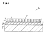
- a photodetector 1 comprises a rectangular plate-shaped substrate 2 made of InP and contact layers 3, 5, a semiconductor multilayer body 4, electrodes 6, 7, and an optical element 10 which are stacked thereon.
- This photodetector 1 is a photodetector which utilizes light absorption of quantum intersubband transitions in the semiconductor multilayer body 4.
- the contact layer (second contact layer) 3 is provided throughout a surface 2a of the substrate 2. At the center of a surface 3a of the contact layer 3, the semiconductor multilayer body 4 having an area smaller than the whole area of the surface 3 is disposed. That is, the semiconductor multilayer body 4 is arranged so as to be contained in the contact layer 3 when seen as a plane. In a peripheral region free of the semiconductor multilayer body 4 in the surface 3a, the electrode (second electrode) 6 is formed like a ring so as to surround the semiconductor multilayer body 4.
- the contact layer (first contact layer) 5 is provided throughout a surface 4a of the semiconductor multilayer body 4. At the center of a surface 5a of the contact layer 5, the optical element 10 having an area smaller than the whole area of the surface 5a is disposed. That is, the optical element 10 is arranged so as to be contained in the contact layer 5 when seen as a plane. In a peripheral region free of the optical element 10 in the surface 5a, the electrode (first electrode) 7 is formed like a ring so as to surround the optical element 10.
- the semiconductor multilayer body 4 has a multiple quantum well structure (or multiple quantum cascade structure) designed so as to correspond to the wavelength of the light to be detected, in which, specifically, semiconductor layers of InGaAs and InAlAs having respective energy bandgaps different from each other are stacked alternately with a thickness of several nm each.
- the contact layers 3, 5, which are made of InGaAs, are respective layers for electrically linking the semiconductor multilayer body 4 to the electrodes 6, 7 in order to detect a current generated in the semiconductor multilayer body 4.
- the electrodes 6, 7 are made of AuGe, Ti/Pt/Au, or the like.
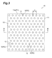
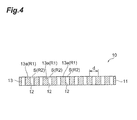
- the optical element 10 is an optical element for transmitting light therethrough from one side to the other side in a predetermined direction and modulating the light. As illustrated in Figs. 3 and 4 , the optical element 10 is equipped with a structure 11, which has first regions R1 and second regions R2 periodically arranged with respect to the first regions R1 along a plane perpendicular to the predetermined direction with a period d which is 1 to 500 ⁇ m according to the wavelength of the incident light.
- the first and second regions R1, R2 have respective refractive indexes different from each other, and properties of transmitting the light incident thereon.
- the structure 11 has a film body 13 provided with a plurality of through holes 12 penetrating therethrough from one side to the other side in the predetermined direction.
- the plurality of through holes 12 are arranged into a triangular lattice when seen as a plane with respect to the film body 13 as illustrated in Fig. 3 , while each through hole 12 has a cylindrical form and penetrates through the film body 13 from one side to the other side in the predetermined direction (the stacking direction of the semiconductor multilayer body 4 in Fig. 2 ) as illustrated in Fig. 4 .
- the film body 13 has a thickness of 10 nm to 2 ⁇ m.
- the first region R1 is a part 13a between the through holes 12 in the film body 13 and specifically made of germanium.
- the second region R2 is a space S within the through hole 12, which is specifically an air. That is, when the photodetector 1 is seen as a plane from the photodetector 10 side (i.e., in Fig. 1 ), a part of the contact layer 5 is seen through the through holes 12.
- the difference between the respective refractive indexes of the first and second regions R1, R2 is preferably 2 or greater, more preferably 3 or greater.
- germanium and the air exhibit refractive indexes of 4.0 and 1.0, respectively, thus yielding a refractive index difference of 3.0 in this embodiment.
- the photodetector 1 is equipped with the optical element 10 as mentioned above, whereby light incident on the optical element 10 from one side in the predetermined direction (e.g., a planar wave incident thereon in the stacking direction of the semiconductor multilayer body 4) is modulated according to the difference between the respective refractive indexes of the first and second regions R1, R2 periodically arranged along a plane perpendicular to the predetermined direction in the structure 11 and then exits from the other side in the predetermined direction. That is, light having no electric field component in the predetermined direction can be modulated efficiently so as to attain an electric field component in the predetermined direction.
- a planar wave incident thereon in the stacking direction of the semiconductor multilayer body 4 e.g., a planar wave incident thereon in the stacking direction of the semiconductor multilayer body
- the optical element 10 Since the plurality of through holes 12 are arranged into a triangular lattice in the film body 13, the optical element 10 depends less on the polarization direction of incident light in particular. While the difference between the respective refractive indexes of the first and second regions R1, R2 is 2 or greater, the period d of arrangement of the first and second regions R1, R2 is 1 to 500 ⁇ m, which is determined according to the wavelength of the incident light, whereby the light is modulated more efficiently.
- the structure 11 in the optical element 10 has the film body 13 provided with a plurality of through holes 12 penetrating therethrough from one side to the other side, the first region R1 is the part 13a between the through holes 12 in the film body 13, and the second region R2 is the space S within the through hole 12. Therefore, the structure 11 can be formed from a single kind of material and thus is inexpensive and easy to manufacture.
- modulated light has an electric field component in the stacking direction of the semiconductor multilayer body 4, so that the electric field component is absorbed into the multiple quantum well structure (or multiple quantum cascade structure), so as to generate a photoelectron, which is detected as a current through the electrodes 6, 7. That is, this photodetector 1 can detect light having no electric field component in the stacking direction of the semiconductor multilayer body 4. Since the photodetector of the present invention further comprises the substrate 2 for supporting the contact layers 5, 6, semiconductor multilayer body 4, and optical element 10, the individual constructions of the photodetector 1 are made stable.
- the photodetector 1 further comprises the electrode 7 formed on the contact layer 5 and the electrode 6 formed on the contact layer 3, the optical element 10 is arranged so as to be contained in the contact layer 5 when seen from one side, the semiconductor multilayer body 4 is arranged so as to be contained in the contact layer 3 when seen from one side, the electrode 7 is formed like a ring in a region free of the optical element 10 in the surface 5a on one side of the contact layer 5 so as to surround the optical element 10, and the electrode 6 is formed like a ring in a region free of the semiconductor multilayer body 4 in the surface 3a on one side of the contact layer 3 so as to surround the semiconductor multilayer body 4. This makes it possible to efficiently detect the current generated in the semiconductor multilayer body 4.
- the surface plasmonic resonance is known as a resonant state of a vibration resultantly occurring when a free electron in a metal combines with an electric field component in light or the like, in order to utilize the surface plasmonic resonance, there is a restriction that the free electron must exist on a surface where the light is incident.
- each of the first and second regions R1, R2 have properties of transmitting the incident light, while no surface plasmonic resonance is utilized for modulating the light, whereby the photosensitivity does not decrease as seen in the photodetector described in the Non-patent Document 1, while materials for use are not limited to metals having free electrons.
- the photodetector described in the Patent Document 1 has a low degree of freedom in designing as a photodetector, since a diffraction grating is formed on a surface of a light-transmitting layer.
- the optical element 10 is formed separately from the contact layer 5, whereby materials having desirable refractive indexes and techniques for forming and processing the optical element 10 can be selected from wide ranges. Therefore, the photodetector 1 of this embodiment has a high degree of freedom in designing according to the wavelength of incident light, desirable photosensitivity, and the like.
- the photodetector 1 of the first embodiment may have the optical element 10 in another mode.
- the plurality of through holes 12 in the film body 13 in the optical element 10 may be arranged into a square lattice instead of the triangular lattice. This achieves a higher efficiency in modulating light when the incident light is linearly polarized light than in the triangular lattice arrangement.
- the photodetector 1 Though a case where light is incident on the optical element 10 from one side in the predetermined direction is explained in the photodetector 1, light may be made incident on the photodetector 1 from the rear side (the other side in the predetermined direction) and detected. This can avoid the optical element 10 from reflecting and absorbing the incident light and thus can further enhance the photosensitivity. Furthermore, while the photodetector 1 is mounted by flip chip bonding onto a package, a submount, IC, or the like, light can easily be made incident thereon, which has a merit in that it expands possibility of developing into image sensors and the like in particular.
- the photodetector of the second embodiment differs from the photodetector 1 of the first embodiment in that an optical element 20 illustrated in Fig. 6 is used in place of the optical element 10.
- the optical element 20 is equipped with a structure 21, which has first regions R1 and second regions R2 periodically arranged with respect to the first regions R1 as in the optical element 10 in the first embodiment.
- the first and second regions R1, R2 have respective refractive indexes different from each other, and properties of transmitting the light incident thereon.
- the structure 21 has a film body 23 provided with a plurality of through holes 22 penetrating therethrough from one side to the other side in the predetermined direction and embedded members 24 held within the respective through holes 22.
- the plurality of through holes 22 and embedded members 24 are arranged into a triangular lattice when seen as a plane with respect to the film body 23 as in the optical element 10 in the first embodiment, while each of the through holes 22 and embedded members 24 has a cylindrical form and penetrates through the film body 23 from one side to the other side in the predetermined direction (the stacking direction of the semiconductor multilayer body 4 in Fig. 2 ) as illustrated in Fig. 6 .
- the film body 23 has a thickness of 10 nm to 2 ⁇ m.
- the first region R1 is a part 23a between the through holes 22 in the film body 23, while the second region R2 is the embedded member 24.
- materials constituting the first region R1 include those of the optical element 10 in the first embodiment.
- materials for constructing the embedded member 24 include silicon dioxide, silicon nitride, and aluminum oxide. Silicon dioxide exhibits a refractive index of 1.3 for mid-infrared light having a wavelength of 5 ⁇ m, for example.
- a material exhibiting a refractive index of 3.3 or greater at this wavelength is preferably used as a material for the first region R1; for example, silicon exhibiting a refractive index of 3.4 for the mid-infrared light having a wavelength of 5 ⁇ m is preferred as a material constituting the first region R1.
- the optical element 20 can select both of materials for the film body 23 and embedded member 24 as mentioned above and thus has a high degree of freedom in adjusting the difference between the refractive indexes of the first and second regions R1, R2.
- the photodetector of the third embodiment differs from the photodetector 1 of the first embodiment in that an optical element 30 illustrated in Fig. 7 is used in place of the optical element 10.
- the optical element 30 is equipped with a structure 31, which has a first region R1 and second regions R2 periodically arranged with respect to the first region R1 as in the optical element 10 in the first embodiment.
- the first and second regions R1, R2 have respective refractive indexes different from each other, and properties of transmitting the light incident thereon.
- the structure 31 has a plurality of depressions 32 opening to one side.
- the plurality of depressions 32 are arranged into a triangular lattice when seen as a plane with respect to the film body 33 as in the optical element 10 in the first embodiment, while each depression 32 has a cylindrical form.
- the film body 33 has a thickness of 10 nm to 2 ⁇ m.
- the first region R1 is a part 33a between the depressions 32 in the film body 33, while the second region R2 is a space S within the depression 32.
- Examples of materials constituting the first and second regions R1, R2 include those of the optical element in the first embodiment.
- the optical element 30 has no through holes penetrating therethrough from one side to the other side in the predetermined direction as mentioned above, so that fine particles in the air and the like do not physically pass from one side to the other side. That is, the optical element 30 acts as a surface protecting material for the photodetector of this embodiment employing the optical element 30, whereby the photodetector is restrained from deteriorating.
- the photodetector of the third embodiment may have the optical element 30 in another mode.
- the plurality of depressions 32 may open to the other side instead of the one side in the optical element 30.
- Embedded members may be held within the depressions 32 as in the optical element 20 in the second embodiment.
- the photodetector of the fourth embodiment differs from the photodetector 1 of the first embodiment in that an optical element 40 illustrated in Figs. 9 and 10 is used in place of the optical element 10.
- the optical element 40 is equipped with a structure 41, which has first regions R1 and second regions R2 periodically arranged with respect to the first regions R1 as in the optical element 10 in the first embodiment.
- the first and second regions R1, R2 have respective refractive indexes different from each other, and properties of transmitting the light incident thereon.
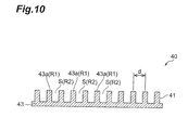
- the structure 41 has a film body 43 provided with a plurality of projections 43a projecting to one side.
- the plurality of projections 43a are arranged into a triangular lattice when seen as a plane with respect to the film body 43 as in the optical element 10 in the first embodiment, while each depression 43a has a cylindrical form and projects from the other side to the one side in the predetermined direction as illustrated in Figs. 9 and 10 .
- the film body 43 has a thickness (including the height of the projection 43a) of 10 nm to 2 ⁇ m.
- the first region R1 is the projection 43a in the film body 43, while the second region R2 is a space S between the projections 43a.
- Examples of materials constituting the first and second regions R1, R2 include those of the optical element 10 in the first embodiment.
- the photodetector of the fourth embodiment may have the optical element 40 in another mode.
- the plurality of projections 43a may project from the one side to the other side in the optical element 40.
- Embedded members may be held between the projections 43a as in the optical element 20 in the second embodiment.
- the photodetector of the fifth embodiment differs from the photodetector 1 of the first embodiment in that through holes in its optical element 10 have a slit form as illustrated in Fig. 11 instead of the cylindrical form.
- the slit-shaped through holes 12 are arranged in a row in a direction perpendicular to the longitudinal direction of the slit form.
- This optical element 10 has a characteristic feature of yielding a higher efficiency for modulating light when the incident light is linearly polarized light as compared with the optical element 10 illustrated in Fig. 5 .
- the photodetector of the sixth embodiment differs from the photodetector 1 of the first embodiment in that an optical element 50 illustrated in Figs. 12 and 13 is used in place of the optical element 10.
- the optical element 50 is equipped with a structure 51, which has first regions R1 and second regions R2 periodically arranged with respect to the first regions R1.
- the first and second regions R1, R2 have respective refractive indexes different from each other, and properties of transmitting the light incident thereon.
- the structure 51 is constructed by arranging a plurality of cylindrical bodies 53a having the same form with a height in the predetermined direction into a triangle lattice along a plane perpendicular to the predetermined direction when seen as a plane.
- the height of the cylindrical body 53a is 10 nm to 2 ⁇ m.
- the first region R1 is the cylindrical body 53a, while the second region R2 is a space S between the cylindrical bodies 53a.
- Examples of the respective materials for constituting the first and second regions R1, R2 include those for the second and first regions R2, R1 in the optical element 10 in the first embodiment.
- the photodetector of the sixth embodiment may have its optical element 50 in another mode.
- the plurality of cylindrical bodies 53a may be arranged into a square lattice instead of the triangular lattice.
- the part constituting the first region may be formed by a plurality of rod-shaped bodies extending in a direction perpendicular to the predetermined direction, instead of the plurality of cylindrical bodies having a height in the predetermined direction, which are arranged on the same plane as with the slit forms in the optical element in the fifth embodiment, so as to construct the structure.
- the photodetector 100 of the seventh embodiment differs from the photodetector 1 of the first embodiment in that, as illustrated in Fig. 14 , the contact layer 5 is provided not throughout the surface 4a of the semiconductor multilayer body 4 but only directly under the electrode 7 and consequently that the optical element 10 is directly disposed on the surface 4a of the semiconductor multilayer body 4.
- results of calculations Fig. 16
- when light passes through an optical element electric field components in the predetermined direction appear most strongly in the vicinity of the surface on the light exit side of the optical element. Since the optical element 10 and semiconductor multilayer body 4 are directly in contact with each other, the photodetector 100 of this embodiment exhibits a higher sensitivity for detecting light than the photodetector 1 of the first embodiment.
- the photodetector of the seventh embodiment may have the optical element 10 in another mode.
- the optical elements in the second to sixth embodiments may be employed in place of the optical element 10.
- a material known as metamaterial whose permittivity and permeability are artificially manipulated by a fine processing technique as disclosed in a literature ( M. Choi et al., "A terahertz metamaterial with unnaturally high refractive index", Nature, 470, 369 (2011 )) may be used as a material constituting the first and second regions.
- the optical element may generate an electric field component in a predetermined direction either when light is incident thereon from one side in the predetermined direction or through the semiconductor multilayer body from the other side. That is, the optical element of the present invention generates an electric field component in a predetermined direction when light is incident thereon along the predetermined direction.
- An electric field strength distribution near the light exit side was calculated for the optical element in the present invention. How the conversion efficiency into an electric field component in the predetermined direction varied when changing the difference between the respective refractive indexes of the first and second regions was also calculated for the optical element in the present invention.
- the optical element 10 illustrated in Fig. 13 was employed.
- the thickness of the optical element 10 and the constituent materials and sizes of the first and second regions R1, R2 are as follows:
- Figs. 15 and 16 illustrate the results.
- the incident light is a planar wave having a wavelength of 5 ⁇ m directed from the lower side to the upper side in Fig. 16 (i.e., in the predetermined direction).
- Fig. 15 illustrates the strength of an electric field component in a direction along a plane formed by the first and second regions R1, R2 (i.e., a plane perpendicular to the predetermined direction) in the optical element 10, while Fig. 16 illustrates the strength of an electric field component perpendicular to this plane.
- the optical element is not necessarily made of a metal (intervention of free electrons is unnecessary). That is, it has been derived from a simulation that effects on a par with or better than those in the case utilizing a metal can be obtained by employing a periodic structure made of a material having no free electrons such as a dielectric body.
- Fig. 17 illustrates the results. It is seen from Fig.
- the conversion efficiency of the electric field component was similarly calculated.
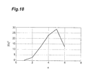
- the optical element 40 was configured such that the first region R1 had a diameter of 1.75 ⁇ m, a thickness of 0.25 ⁇ m, and a period d of 2.9 ⁇ m with respect to the second region R2. How the efficiency in converting an electric field component in a direction perpendicular to the predetermined direction into an electric field component in the predetermined direction varied when changing the refractive index of the first region R1 was calculated.
- Fig. 18 illustrates the results. It is seen from Fig.
- the optical element 50 is one in which a plurality of rod-shaped bodies 53b (first regions R1) each extending in a direction perpendicular to a predetermined direction are arranged in parallel with each other so as to form stripes with spaces S (second region R2).
- the photodetector 200 differs from the photodetector 1 in that it uses the optical element 50 and a substrate 2 constituted by n-type InP and that the second electrode 6 is disposed throughout a surface 2b of the substrate 2 on the side opposite from the surface 2a.
- Fig. 21 illustrates results of a simulation.
- D indicates the linewidth ( ⁇ m) of germanium. It is seen from these results that the perpendicular electric field intensity tends to become greater with respect to the incident light in the infrared region when the linewidth of germanium is not smaller than that of the air (i.e., when the width of the first region is not smaller than that of the second region). For example, acute peaks are seen in a wavelength region where the ratio of germanium to air is 2.8:0.4 to 3.1:0.1.
- the maximum perpendicular electric field is seen to be obtained when infrared light having a wavelength of 3.7 ⁇ m or 5.3 ⁇ m is incident in the case where the linewidth of germanium is 3.0 ⁇ m.
- the optical element can be designed in terms of the relationship between the period and linewidth (or diameter) of the first and second regions or the interrelationship between two kinds of linewidth so as to maximize the electric field intensity obtained at the wavelength of incident light.
Landscapes
- Physics & Mathematics (AREA)
- Chemical & Material Sciences (AREA)
- Crystallography & Structural Chemistry (AREA)
- General Physics & Mathematics (AREA)
- Optics & Photonics (AREA)
- Light Receiving Elements (AREA)
- Polarising Elements (AREA)
Abstract
Description
- The present invention relates to an optical element for transmitting light therethrough and modulating the light and a photodetector equipped therewith.
- Known as photodetectors utilizing light absorption of quantum intersubband transitions are QWIP (quantum well type infrared optical sensor), QDIP (quantum dot infrared optical sensor), QCD (quantum cascade type optical sensor), and the like. They utilize no energy bandgap transitions and thus have such merits as high degree of freedom in designing wavelength ranges, low dark current, and operability at room temperature.
- Among these photodetectors, the QWIP and QCD are equipped with a semiconductor multilayer body having a periodic multilayer structure such as a quantum well structure or quantum cascade structure. This semiconductor multilayer body generates a current due to an electric field component in the stacking direction thereof only when light incident thereon has such an electric field component, and thus is not photosensitive to light having no electric field component in the stacking direction (planar waves incident thereon in the stacking direction thereof).
- Therefore, in order for the QWIP or QCD to detect light, it is necessary for the light to be incident thereon such that a direction of vibration of an electric field of the light coincides with the stacking direction of the semiconductor multilayer body. When detecting a planar wave having a wavefront perpendicular to an advancing direction of light, for example, it is necessary for the light to be incident on the semiconductor multilayer body in a direction perpendicular to its stacking direction, which makes the photodetector cumbersome to use.
- There has hence been known a photodetector which, for detecting light having no electric field component in the stacking direction of the semiconductor multilayer body, a thin gold film is disposed on a surface of the semiconductor multilayer body and periodically formed with holes each having a diameter not greater than the wavelength of the light (see Non-patent Document 1). In this example, the light is modulated so as to attain an electric field component in the stacking direction of the semiconductor multilayer body under a surface plasmonic resonance effect on the thin gold film.
- There has also been known a photodetector in which a light-transmitting layer is disposed on a surface of a semiconductor multilayer body, while a diffraction grating constituted by a pattern of irregularities and a reflective film covering the same are formed on the light-transmitting layer (see Patent Document 1). In this example, the light is modulated so as to attain an electric field component in the stacking direction of the semiconductor multilayer body under the effects of diffraction and reflection of the incident light by the diffraction grating and reflective film.
- [Patent Document 1] Japanese Patent Application Laid-Open No.
2000-156513 - [Non-patent Document 1] W. Wu, et al., "Plasmonic enhanced quantum well infrared photodetector with high detectivity", Appl. Phys. Lett., 96, 161107 (2010)
- Thus, for detecting light having no electric field component in the stacking direction of the semiconductor multilayer body, various techniques for modulating the light so as to provide it with an electric field component in the stacking direction have been proposed and desired to attain higher efficiency in such modulation of light.
- That is, assuming the stacking direction of the semiconductor multilayer body to be a predetermined direction, there has been a demand for a technique which efficiently modulates light having no electric field component in the predetermined direction such that the light attains an electric field component in the predetermined direction.
- It is therefore an object of the present invention to provide an optical element which can efficiently modulate light having no electric field component in a predetermined direction such that the light attains an electric field component in the predetermined direction and a photodetector which, by using a semiconductor multilayer body having a quantum well structure, a quantum cascade structure, or the like, can detect light having no electric field component in the stacking direction of the semiconductor multilayer body.
- The optical element in accordance with the present invention is an optical element for transmitting light therethrough along a predetermined direction and modulating the light, the optical element comprising a structure having first regions and second regions periodically arranged with respect to the first regions along a plane perpendicular to the predetermined direction, the first and second regions having respective refractive indexes different from each other, and properties of transmitting the light therethrough.
- Light incident on this optical element along a predetermined direction is modulated according to the difference between the respective refractive indexes of the first and second regions periodically arranged along a plane perpendicular to the predetermined direction in the structure and then exits therefrom along the predetermined direction. That is, light having no electric field component in a predetermined direction can efficiently be modulated such as to attain an electric field component in the predetermined direction.
- Here, the difference between the refractive indexes of the first and second regions may be 2 or greater. The first and second regions may be arranged with a period of 1 to 500 µm. This can modulate light having no electric field component in a predetermined direction more efficiently so as to provide it with an electric field component in the predetermined direction.
- The light transmitted through the optical element of the present invention may be an infrared ray. This allows the optical element of the present invention to be applied favorably to infrared photodetectors.
- The structure in the optical element of the present invention may have a film body provided with a plurality of through holes penetrating therethrough along the predetermined direction, the first region being a part between the through holes in the film body, the second region being a space within the through hole. The structure in the optical element of the present invention may have a film body provided with a plurality of depressions opening to one side or the other side in the predetermined direction, the first region being a part between the depressions in the film body, the second region being a space within the depression. The structure in the optical element of the present invention may have a film body provided with a plurality of projections projecting to one side or the other side in the predetermined direction, the first region being the projection, the second region being a space between the projections. The structure having such a film body is inexpensive and easy to manufacture, since it can be formed from a single kind of material. The mode of the structure can be selected from the above as appropriate so that light having no electric field component in a predetermined direction can be modulated more efficiently so as to attain an electric field component in the predetermined direction.
- The structure in the optical element of the present invention may have a film body provided with a plurality of through holes penetrating therethrough along the predetermined direction and an embedded member held within the through hole, the first region being a part between the through holes in the film body, the second region being the embedded member. The structure in the optical element of the present invention may have a film body provided with a plurality of depressions opening to one side or the other side in the predetermined direction and an embedded member held within the through hole, the first region being a part between the depressions in the film body, the second region being the embedded member. The structure in the optical element of the present invention may have a film body provided with a plurality of projections projecting to one side or the other side in the predetermined direction and an embedded member held between the projections, the first region being the projection, the second region being the embedded member. These make it possible to select both of materials for the film body and embedded member, thereby enhancing the degree of freedom in adjusting the difference between the refractive indexes of the first and second regions.
- The photodetector of the present invention comprises the above-mentioned optical element, a semiconductor multilayer body arranged on the other side opposite to one side in the predetermined direction with respect to the optical element and adapted to generate a current due to an electric field component in the predetermined direction in the light transmitted through the optical element, a first contact layer formed on a surface on the one side of the semiconductor multilayer body, and a second contact layer formed on a surface on the other side of the semiconductor multilayer body.
- Since this photodetector is equipped with the above-mentioned optical element, the light incident thereon is modulated in the process of being transmitted through the optical element. The modulated light has an electric field component in the stacking direction of the semiconductor multilayer body, so that the electric field component generates a current in the semiconductor multilayer body. That is, by using a semiconductor multilayer body having a quantum well structure, a quantum cascade structure, or the like, this photodetector can detect light having no electric field component in the stacking direction of the semiconductor multilayer body.
- The photodetector of the present invention may further comprise a substrate having the second contact layer, semiconductor multilayer body, first contact layer, and optical element sequentially stacked thereon from the other side. This can stabilize individual constructions of the photodetector.
- The photodetector of the present invention may further comprise a first electrode electrically connected to the first contact layer and a second electrode electrically connected to the second contact layer. This makes it possible to efficiently detect the current generated in the semiconductor multilayer body.
- In the photodetector of the present invention, the optical element may generate the electric field component in the predetermined direction either when light is incident thereon from the one side or through the semiconductor multilayer body from the other side.
- The present invention can provide an optical element which can efficiently modulate light having no electric field component in a predetermined direction such that the light attains an electric field component in the predetermined direction and a photodetector which, by using a semiconductor multilayer body having a quantum well structure, a quantum cascade structure, or the like, can detect light having no electric field component in the stacking direction of the semiconductor multilayer body.
-
-
Fig. 1 is a plan view of the photodetector in accordance with a first embodiment of the present invention; -
Fig. 2 is a sectional view taken along the line II-II ofFig. 1 ; -
Fig. 3 is a plan view of the optical element in accordance with the first embodiment of the present invention; -
Fig. 4 is a sectional view taken along the line IV-IV ofFig. 3 ; -
Fig. 5 is a plan view of a modified example of the optical element in accordance with the first embodiment of the present invention; -
Fig. 6 is a sectional view of the optical element in accordance with a second embodiment of the present invention; -
Fig. 7 is a sectional view of the optical element in accordance with a third embodiment of the present invention; -
Fig. 8 is a sectional view of a modified example of the optical element in accordance with the third embodiment of the present invention; -
Fig. 9 is a plan view of the photodetector in accordance with a fourth embodiment of the present invention; -
Fig. 10 is an end face view taken along the line X-X ofFig. 9 ; -
Fig. 11 is a plan view of the optical element in accordance with a fifth embodiment of the present invention; -
Fig. 12 is a plan view of the optical element in accordance with a sixth embodiment of the present invention; -
Fig. 13 is an end face view taken along the line XIII-XIII ofFig. 12 ; -
Fig. 14 is a sectional view of the optical element in accordance with the sixth embodiment of the present invention; -
Fig. 15 is an electric field strength distribution according to an FDTD method concerning the optical element ofFig. 11 ; -
Fig. 16 is an electric field strength distribution according to the FDTD method concerning the optical element ofFig. 11 ; -
Fig. 17 is a graph illustrating the conversion efficiency of an electric field component vs. the refractive index difference concerning the optical element ofFig. 11 ; and -
Fig. 18 is a graph illustrating the conversion efficiency of an electric field component vs. the refractive index difference concerning the optical element ofFigs. 9 and10 . -
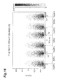
Fig. 19 is a plan view of a photodetector used in a simulation; -
Fig. 20 is a sectional view taken along the line XX-XX ofFig. 19 ; and -
Fig. 21 is a perpendicular electric field intensity spectrum according to the FDTD method concerning the optical element used in the photodetector ofFig. 19 . - In the following, preferred embodiments of the present invention will be explained with reference to the drawings. The same or equivalent parts in the drawings will be referred to with the same signs, while omitting their overlapping descriptions. By "refractive index" in the specification is meant the refractive index for incident light. The light to be detected by photodetectors of the embodiments is an infrared ray (light having a wavelength of 2 to 1000 µm).
- As illustrated in
Figs. 1 and2 , aphotodetector 1 comprises a rectangular plate-shapedsubstrate 2 made of InP andcontact layers semiconductor multilayer body 4,electrodes optical element 10 which are stacked thereon. Thisphotodetector 1 is a photodetector which utilizes light absorption of quantum intersubband transitions in thesemiconductor multilayer body 4. - The contact layer (second contact layer) 3 is provided throughout a
surface 2a of thesubstrate 2. At the center of asurface 3a of thecontact layer 3, thesemiconductor multilayer body 4 having an area smaller than the whole area of thesurface 3 is disposed. That is, thesemiconductor multilayer body 4 is arranged so as to be contained in thecontact layer 3 when seen as a plane. In a peripheral region free of thesemiconductor multilayer body 4 in thesurface 3a, the electrode (second electrode) 6 is formed like a ring so as to surround thesemiconductor multilayer body 4. - The contact layer (first contact layer) 5 is provided throughout a
surface 4a of thesemiconductor multilayer body 4. At the center of asurface 5a of thecontact layer 5, theoptical element 10 having an area smaller than the whole area of thesurface 5a is disposed. That is, theoptical element 10 is arranged so as to be contained in thecontact layer 5 when seen as a plane. In a peripheral region free of theoptical element 10 in thesurface 5a, the electrode (first electrode) 7 is formed like a ring so as to surround theoptical element 10. - The
semiconductor multilayer body 4 has a multiple quantum well structure (or multiple quantum cascade structure) designed so as to correspond to the wavelength of the light to be detected, in which, specifically, semiconductor layers of InGaAs and InAlAs having respective energy bandgaps different from each other are stacked alternately with a thickness of several nm each. - The contact layers 3, 5, which are made of InGaAs, are respective layers for electrically linking the
semiconductor multilayer body 4 to theelectrodes semiconductor multilayer body 4. Theelectrodes - The
optical element 10 is an optical element for transmitting light therethrough from one side to the other side in a predetermined direction and modulating the light. As illustrated inFigs. 3 and4 , theoptical element 10 is equipped with astructure 11, which has first regions R1 and second regions R2 periodically arranged with respect to the first regions R1 along a plane perpendicular to the predetermined direction with a period d which is 1 to 500 µm according to the wavelength of the incident light. The first and second regions R1, R2 have respective refractive indexes different from each other, and properties of transmitting the light incident thereon. - The
structure 11 has afilm body 13 provided with a plurality of throughholes 12 penetrating therethrough from one side to the other side in the predetermined direction. The plurality of throughholes 12 are arranged into a triangular lattice when seen as a plane with respect to thefilm body 13 as illustrated inFig. 3 , while each throughhole 12 has a cylindrical form and penetrates through thefilm body 13 from one side to the other side in the predetermined direction (the stacking direction of thesemiconductor multilayer body 4 inFig. 2 ) as illustrated inFig. 4 . Preferably, thefilm body 13 has a thickness of 10 nm to 2 µm. - Here, the first region R1 is a
part 13a between the throughholes 12 in thefilm body 13 and specifically made of germanium. The second region R2 is a space S within the throughhole 12, which is specifically an air. That is, when thephotodetector 1 is seen as a plane from thephotodetector 10 side (i.e., inFig. 1 ), a part of thecontact layer 5 is seen through the through holes 12. The difference between the respective refractive indexes of the first and second regions R1, R2 is preferably 2 or greater, more preferably 3 or greater. For mid-infrared light having a wavelength of 5 µm, for example, germanium and the air exhibit refractive indexes of 4.0 and 1.0, respectively, thus yielding a refractive index difference of 3.0 in this embodiment. - The
photodetector 1 is equipped with theoptical element 10 as mentioned above, whereby light incident on theoptical element 10 from one side in the predetermined direction (e.g., a planar wave incident thereon in the stacking direction of the semiconductor multilayer body 4) is modulated according to the difference between the respective refractive indexes of the first and second regions R1, R2 periodically arranged along a plane perpendicular to the predetermined direction in thestructure 11 and then exits from the other side in the predetermined direction. That is, light having no electric field component in the predetermined direction can be modulated efficiently so as to attain an electric field component in the predetermined direction. Since the plurality of throughholes 12 are arranged into a triangular lattice in thefilm body 13, theoptical element 10 depends less on the polarization direction of incident light in particular. While the difference between the respective refractive indexes of the first and second regions R1, R2 is 2 or greater, the period d of arrangement of the first and second regions R1, R2 is 1 to 500 µm, which is determined according to the wavelength of the incident light, whereby the light is modulated more efficiently. Thestructure 11 in theoptical element 10 has thefilm body 13 provided with a plurality of throughholes 12 penetrating therethrough from one side to the other side, the first region R1 is thepart 13a between the throughholes 12 in thefilm body 13, and the second region R2 is the space S within the throughhole 12. Therefore, thestructure 11 can be formed from a single kind of material and thus is inexpensive and easy to manufacture. - Thus modulated light has an electric field component in the stacking direction of the
semiconductor multilayer body 4, so that the electric field component is absorbed into the multiple quantum well structure (or multiple quantum cascade structure), so as to generate a photoelectron, which is detected as a current through theelectrodes photodetector 1 can detect light having no electric field component in the stacking direction of thesemiconductor multilayer body 4. Since the photodetector of the present invention further comprises thesubstrate 2 for supporting the contact layers 5, 6,semiconductor multilayer body 4, andoptical element 10, the individual constructions of thephotodetector 1 are made stable. Thephotodetector 1 further comprises theelectrode 7 formed on thecontact layer 5 and theelectrode 6 formed on thecontact layer 3, theoptical element 10 is arranged so as to be contained in thecontact layer 5 when seen from one side, thesemiconductor multilayer body 4 is arranged so as to be contained in thecontact layer 3 when seen from one side, theelectrode 7 is formed like a ring in a region free of theoptical element 10 in thesurface 5a on one side of thecontact layer 5 so as to surround theoptical element 10, and theelectrode 6 is formed like a ring in a region free of thesemiconductor multilayer body 4 in thesurface 3a on one side of thecontact layer 3 so as to surround thesemiconductor multilayer body 4. This makes it possible to efficiently detect the current generated in thesemiconductor multilayer body 4. - In the photodetector described in the
Non-patent Document 1, a part of incident light (an infrared ray) is blocked by a thin gold film, while the surface plasmonic resonance itself incurs such a large energy loss as to lower photosensitivity. Since the surface plasmonic resonance is known as a resonant state of a vibration resultantly occurring when a free electron in a metal combines with an electric field component in light or the like, in order to utilize the surface plasmonic resonance, there is a restriction that the free electron must exist on a surface where the light is incident. In thephotodetector 1 of this embodiment, by contrast, each of the first and second regions R1, R2 have properties of transmitting the incident light, while no surface plasmonic resonance is utilized for modulating the light, whereby the photosensitivity does not decrease as seen in the photodetector described in theNon-patent Document 1, while materials for use are not limited to metals having free electrons. - On the other hand, the photodetector described in the
Patent Document 1 has a low degree of freedom in designing as a photodetector, since a diffraction grating is formed on a surface of a light-transmitting layer. In thephotodetector 1 of this embodiment, by contrast, theoptical element 10 is formed separately from thecontact layer 5, whereby materials having desirable refractive indexes and techniques for forming and processing theoptical element 10 can be selected from wide ranges. Therefore, thephotodetector 1 of this embodiment has a high degree of freedom in designing according to the wavelength of incident light, desirable photosensitivity, and the like. - The
photodetector 1 of the first embodiment may have theoptical element 10 in another mode. For example, as illustrated inFig. 5 , the plurality of throughholes 12 in thefilm body 13 in theoptical element 10 may be arranged into a square lattice instead of the triangular lattice. This achieves a higher efficiency in modulating light when the incident light is linearly polarized light than in the triangular lattice arrangement. - Though a case where light is incident on the
optical element 10 from one side in the predetermined direction is explained in thephotodetector 1, light may be made incident on thephotodetector 1 from the rear side (the other side in the predetermined direction) and detected. This can avoid theoptical element 10 from reflecting and absorbing the incident light and thus can further enhance the photosensitivity. Furthermore, while thephotodetector 1 is mounted by flip chip bonding onto a package, a submount, IC, or the like, light can easily be made incident thereon, which has a merit in that it expands possibility of developing into image sensors and the like in particular. - Another embodiment of the photodetector will now be explained as the second embodiment of the present invention. The photodetector of the second embodiment differs from the
photodetector 1 of the first embodiment in that anoptical element 20 illustrated inFig. 6 is used in place of theoptical element 10. - The
optical element 20 is equipped with astructure 21, which has first regions R1 and second regions R2 periodically arranged with respect to the first regions R1 as in theoptical element 10 in the first embodiment. The first and second regions R1, R2 have respective refractive indexes different from each other, and properties of transmitting the light incident thereon. - The
structure 21 has afilm body 23 provided with a plurality of throughholes 22 penetrating therethrough from one side to the other side in the predetermined direction and embedded members 24 held within the respective throughholes 22. The plurality of throughholes 22 and embedded members 24 are arranged into a triangular lattice when seen as a plane with respect to thefilm body 23 as in theoptical element 10 in the first embodiment, while each of the throughholes 22 and embedded members 24 has a cylindrical form and penetrates through thefilm body 23 from one side to the other side in the predetermined direction (the stacking direction of thesemiconductor multilayer body 4 inFig. 2 ) as illustrated inFig. 6 . Preferably, thefilm body 23 has a thickness of 10 nm to 2 µm. - Here, the first region R1 is a
part 23a between the throughholes 22 in thefilm body 23, while the second region R2 is the embedded member 24. Examples of materials constituting the first region R1 include those of theoptical element 10 in the first embodiment. Examples of materials for constructing the embedded member 24 include silicon dioxide, silicon nitride, and aluminum oxide. Silicon dioxide exhibits a refractive index of 1.3 for mid-infrared light having a wavelength of 5 µm, for example. In this case, a material exhibiting a refractive index of 3.3 or greater at this wavelength is preferably used as a material for the first region R1; for example, silicon exhibiting a refractive index of 3.4 for the mid-infrared light having a wavelength of 5 µm is preferred as a material constituting the first region R1. - The
optical element 20 can select both of materials for thefilm body 23 and embedded member 24 as mentioned above and thus has a high degree of freedom in adjusting the difference between the refractive indexes of the first and second regions R1, R2. - Another embodiment of the photodetector will now be explained as the third embodiment of the present invention. The photodetector of the third embodiment differs from the
photodetector 1 of the first embodiment in that anoptical element 30 illustrated inFig. 7 is used in place of theoptical element 10. - The
optical element 30 is equipped with astructure 31, which has a first region R1 and second regions R2 periodically arranged with respect to the first region R1 as in theoptical element 10 in the first embodiment. The first and second regions R1, R2 have respective refractive indexes different from each other, and properties of transmitting the light incident thereon. - The
structure 31 has a plurality ofdepressions 32 opening to one side. The plurality ofdepressions 32 are arranged into a triangular lattice when seen as a plane with respect to thefilm body 33 as in theoptical element 10 in the first embodiment, while eachdepression 32 has a cylindrical form. Preferably, thefilm body 33 has a thickness of 10 nm to 2 µm. - Here, the first region R1 is a
part 33a between thedepressions 32 in thefilm body 33, while the second region R2 is a space S within thedepression 32. Examples of materials constituting the first and second regions R1, R2 include those of the optical element in the first embodiment. - The
optical element 30 has no through holes penetrating therethrough from one side to the other side in the predetermined direction as mentioned above, so that fine particles in the air and the like do not physically pass from one side to the other side. That is, theoptical element 30 acts as a surface protecting material for the photodetector of this embodiment employing theoptical element 30, whereby the photodetector is restrained from deteriorating. - The photodetector of the third embodiment may have the
optical element 30 in another mode. For example, as illustrated inFig. 8 , the plurality ofdepressions 32 may open to the other side instead of the one side in theoptical element 30. Embedded members may be held within thedepressions 32 as in theoptical element 20 in the second embodiment. - Another embodiment of the photodetector will now be explained as the fourth embodiment of the present invention. The photodetector of the fourth embodiment differs from the
photodetector 1 of the first embodiment in that anoptical element 40 illustrated inFigs. 9 and10 is used in place of theoptical element 10. - The
optical element 40 is equipped with astructure 41, which has first regions R1 and second regions R2 periodically arranged with respect to the first regions R1 as in theoptical element 10 in the first embodiment. The first and second regions R1, R2 have respective refractive indexes different from each other, and properties of transmitting the light incident thereon. - The
structure 41 has afilm body 43 provided with a plurality ofprojections 43a projecting to one side. The plurality ofprojections 43a are arranged into a triangular lattice when seen as a plane with respect to thefilm body 43 as in theoptical element 10 in the first embodiment, while eachdepression 43a has a cylindrical form and projects from the other side to the one side in the predetermined direction as illustrated inFigs. 9 and10 . Preferably, thefilm body 43 has a thickness (including the height of theprojection 43a) of 10 nm to 2 µm. - Here, the first region R1 is the
projection 43a in thefilm body 43, while the second region R2 is a space S between theprojections 43a. Examples of materials constituting the first and second regions R1, R2 include those of theoptical element 10 in the first embodiment. - The photodetector of the fourth embodiment may have the
optical element 40 in another mode. For example, the plurality ofprojections 43a may project from the one side to the other side in theoptical element 40. Embedded members may be held between theprojections 43a as in theoptical element 20 in the second embodiment. - Another embodiment of the photodetector will now be explained as the fifth embodiment of the present invention. The photodetector of the fifth embodiment differs from the
photodetector 1 of the first embodiment in that through holes in itsoptical element 10 have a slit form as illustrated inFig. 11 instead of the cylindrical form. - The slit-shaped through
holes 12 are arranged in a row in a direction perpendicular to the longitudinal direction of the slit form. Thisoptical element 10 has a characteristic feature of yielding a higher efficiency for modulating light when the incident light is linearly polarized light as compared with theoptical element 10 illustrated inFig. 5 . - Another embodiment of the photodetector will now be explained as the sixth embodiment of the present invention. The photodetector of the sixth embodiment differs from the
photodetector 1 of the first embodiment in that anoptical element 50 illustrated inFigs. 12 and13 is used in place of theoptical element 10. - The
optical element 50 is equipped with astructure 51, which has first regions R1 and second regions R2 periodically arranged with respect to the first regions R1. The first and second regions R1, R2 have respective refractive indexes different from each other, and properties of transmitting the light incident thereon. - The
structure 51 is constructed by arranging a plurality ofcylindrical bodies 53a having the same form with a height in the predetermined direction into a triangle lattice along a plane perpendicular to the predetermined direction when seen as a plane. Preferably, the height of thecylindrical body 53a is 10 nm to 2 µm. - Here, the first region R1 is the
cylindrical body 53a, while the second region R2 is a space S between thecylindrical bodies 53a. Examples of the respective materials for constituting the first and second regions R1, R2 include those for the second and first regions R2, R1 in theoptical element 10 in the first embodiment. - The photodetector of the sixth embodiment may have its
optical element 50 in another mode. For example, the plurality ofcylindrical bodies 53a may be arranged into a square lattice instead of the triangular lattice. The part constituting the first region may be formed by a plurality of rod-shaped bodies extending in a direction perpendicular to the predetermined direction, instead of the plurality of cylindrical bodies having a height in the predetermined direction, which are arranged on the same plane as with the slit forms in the optical element in the fifth embodiment, so as to construct the structure. - Another embodiment of the photodetector will now be explained as the seventh embodiment of the present invention. The
photodetector 100 of the seventh embodiment differs from thephotodetector 1 of the first embodiment in that, as illustrated inFig. 14 , thecontact layer 5 is provided not throughout thesurface 4a of thesemiconductor multilayer body 4 but only directly under theelectrode 7 and consequently that theoptical element 10 is directly disposed on thesurface 4a of thesemiconductor multilayer body 4. As can be seen from results of calculations (Fig. 16 ) which will be explained later, when light passes through an optical element, electric field components in the predetermined direction appear most strongly in the vicinity of the surface on the light exit side of the optical element. Since theoptical element 10 andsemiconductor multilayer body 4 are directly in contact with each other, thephotodetector 100 of this embodiment exhibits a higher sensitivity for detecting light than thephotodetector 1 of the first embodiment. - The photodetector of the seventh embodiment may have the
optical element 10 in another mode. For example, the optical elements in the second to sixth embodiments may be employed in place of theoptical element 10. - Though preferred embodiments of the present invention have been explained in the foregoing, the present invention is not limited thereto at all. For example, a material known as metamaterial whose permittivity and permeability are artificially manipulated by a fine processing technique as disclosed in a literature (M. Choi et al., "A terahertz metamaterial with unnaturally high refractive index", Nature, 470, 369 (2011)) may be used as a material constituting the first and second regions.
- In the photodetector of the present invention, the optical element may generate an electric field component in a predetermined direction either when light is incident thereon from one side in the predetermined direction or through the semiconductor multilayer body from the other side. That is, the optical element of the present invention generates an electric field component in a predetermined direction when light is incident thereon along the predetermined direction.
- An electric field strength distribution near the light exit side was calculated for the optical element in the present invention. How the conversion efficiency into an electric field component in the predetermined direction varied when changing the difference between the respective refractive indexes of the first and second regions was also calculated for the optical element in the present invention.
- The
optical element 10 illustrated inFig. 13 was employed. The thickness of theoptical element 10 and the constituent materials and sizes of the first and second regions R1, R2 are as follows: - Thickness of the optical element: 0.5 µm
- First region: germanium (refractive index 4.0), width 0.7 µm
- Second region: air (refractive index 1.0), width 0.8 µm
- The electric field strength distribution was calculated by a successive approximation method known as FDTD (Finite-Difference Time-Domain) method.
Figs. 15 and16 illustrate the results. Here, the incident light is a planar wave having a wavelength of 5 µm directed from the lower side to the upper side inFig. 16 (i.e., in the predetermined direction).Fig. 15 illustrates the strength of an electric field component in a direction along a plane formed by the first and second regions R1, R2 (i.e., a plane perpendicular to the predetermined direction) in theoptical element 10, whileFig. 16 illustrates the strength of an electric field component perpendicular to this plane. - The results of calculations have verified that the incident light is modulated while passing through the first and second regions R1, R2 in the
optical element 10, so that at least a part of light having no electric field component in the predetermined direction attains an electric field component in the predetermined direction. It has been seen fromFig. 16 that the electric field component in the predetermined direction extends in the exiting direction of the incident light from near the boundary between the first and second regions R1, R2 in the exit-side surface of theoptical element 10 in the vicinity of theoptical element 10, so as to localize. On the other hand, an electric field component not converted to an electric field component in the predetermined direction by the modulation of the incident light has been seen to propagate to the far side of theoptical element 10 together with the light having passed through the first and second regions R1, R2. - In other words, as is clear from
Fig. 16 , an electric field component in the light propagation direction, which cannot occur in light propagating through free spaces, is seen to occur. While the electric field component extending along the plane formed by the first and second regions R1, R2 propagates to parts distanced from theoptical element 10 as illustrated inFig. 15 , the electric field component in the predetermined direction localizes in the vicinity of theoptical element 10 as illustrated inFig. 16 . This shows that the action by theoptical element 10 is not caused by a simple diffraction as disclosed in thePatent Document 1. - The results of calculations show that, in order for light having no electric field component in the predetermined direction to be modulated such as to attain an electric field component in the predetermined direction, the optical element is not necessarily made of a metal (intervention of free electrons is unnecessary). That is, it has been derived from a simulation that effects on a par with or better than those in the case utilizing a metal can be obtained by employing a periodic structure made of a material having no free electrons such as a dielectric body.
- Next, how the conversion efficiency into an electric field component in the predetermined direction varied when changing the difference between the respective refractive indexes of the first and second regions was calculated. The thickness of the above-mentioned
optical element 10 was changed to 0.2 µm, and how the efficiency in converting an electric field component in a direction perpendicular to the predetermined direction into an electric field component in the predetermined direction varied when changing the refractive index of the first region R1 was calculated.Fig. 17 illustrates the results. It is seen fromFig. 17 that an electric field component in the predetermined direction does not occur when the refractive index n of the first region is 1.0, i.e., equal to that of the air constituting the second region, but the strength of the electric field component in the predetermined direction increases as the refractive index of the first region R1 becomes greater. - Using the
optical element 40 illustrated inFigs. 9 and10 , the conversion efficiency of the electric field component was similarly calculated. Theoptical element 40 was configured such that the first region R1 had a diameter of 1.75 µm, a thickness of 0.25 µm, and a period d of 2.9 µm with respect to the second region R2. How the efficiency in converting an electric field component in a direction perpendicular to the predetermined direction into an electric field component in the predetermined direction varied when changing the refractive index of the first region R1 was calculated.Fig. 18 illustrates the results. It is seen fromFig. 18 that an electric field component in the predetermined direction does not occur when the refractive index n of the first region is 1.0, i.e., equal to that of the air, but the strength of the electric field component in the predetermined direction increases as the refractive index of the first region R1 becomes greater. Thus obtained strength of the electric field component is four times that of theoptical element 10 ofFig. 11 for which the results of calculations are illustrated inFig. 17 . - While the period in the first region (germanium) and second region (air) was kept constant at 3.2 µm, how the spectrum of perpendicular electric field intensity varied when their width ratio was changed was calculated by the FDTD method. The thickness of the first and second regions was 0.8 µm.
- An
optical element 50 and aphotodetector 200 which are illustrated inFigs. 19 and20 were used as subjects. Theoptical element 50 is one in which a plurality of rod-shapedbodies 53b (first regions R1) each extending in a direction perpendicular to a predetermined direction are arranged in parallel with each other so as to form stripes with spaces S (second region R2). Thephotodetector 200 differs from thephotodetector 1 in that it uses theoptical element 50 and asubstrate 2 constituted by n-type InP and that thesecond electrode 6 is disposed throughout asurface 2b of thesubstrate 2 on the side opposite from thesurface 2a. -
Fig. 21 illustrates results of a simulation. InFig. 21 , D indicates the linewidth (µm) of germanium. It is seen from these results that the perpendicular electric field intensity tends to become greater with respect to the incident light in the infrared region when the linewidth of germanium is not smaller than that of the air (i.e., when the width of the first region is not smaller than that of the second region). For example, acute peaks are seen in a wavelength region where the ratio of germanium to air is 2.8:0.4 to 3.1:0.1. In particular, the maximum perpendicular electric field is seen to be obtained when infrared light having a wavelength of 3.7 µm or 5.3 µm is incident in the case where the linewidth of germanium is 3.0 µm. Utilizing such a simulation, the optical element can be designed in terms of the relationship between the period and linewidth (or diameter) of the first and second regions or the interrelationship between two kinds of linewidth so as to maximize the electric field intensity obtained at the wavelength of incident light. - 1, 100, 200...photodetector; 2...substrate; 3, 5...contact layer; 4... semiconductor multilayer body; 6, 7...electrode; 10, 20, 30, 40, 50...optical element; 11, 21, 31, 41, 51...structure; 12, 22...through hole; 13, 23, 33, 43...film body; 13a, 23a...part between through holes; 23a...part between depressions; 24...embedded member; 32...depression; 33a...part between depressions; 43a...projection; R1... first region; R2... second region; S... space
Claims (15)
- An optical element for transmitting light therethrough along a predetermined direction and modulating the light,
the optical element comprising a structure having first regions and second regions periodically arranged with respect to the first regions along a plane perpendicular to the predetermined direction;
wherein the first and second regions have respective refractive indexes different from each other, and properties of transmitting the light therethrough. - The optical element according to claim 1, wherein the difference between the refractive indexes of the first and second regions is 2 or greater.
- The optical element according to claim 1 or 2, wherein the first and second regions are arranged with a period of 1 to 500 µm.
- The optical element according to any one of claims 1 to 3, wherein the light is an infrared ray.
- The optical element according to any one of claims 1 to 4, wherein the structure has a film body provided with a plurality of through holes penetrating therethrough along the predetermined direction;
wherein the first region is a part between the through holes in the film body; and
wherein the second region is a space within the through hole. - The optical element according to any one of claims 1 to 4, wherein the structure has a film body provided with a plurality of through holes penetrating therethrough along the predetermined direction and an embedded member held within the through hole;
wherein the first region is a part between the through holes in the film body; and
wherein the second region is the embedded member. - The optical element according to any one of claims 1 to 4, wherein the structure has a film body provided with a plurality of depressions opening to one side or the other side in the predetermined direction;
wherein the first region is a part between the depressions in the film body; and
wherein the second region is a space within the depression. - The optical element according to any one of claims 1 to 4, wherein the structure has a film body provided with a plurality of depressions opening to one side or the other side in the predetermined direction and an embedded member held within the through hole;
wherein the first region is a part between the depressions in the film body; and
wherein the second region is the embedded member. - The optical element according to any one of claims 1 to 4, wherein the structure has a film body provided with a plurality of projections projecting to one side or the other side in the predetermined direction;
wherein the first region is the projection; and
wherein the second region is a space between the projections. - The optical element according to any one of claims 1 to 4, wherein the structure has a film body provided with a plurality of projections projecting to one side or the other side in the predetermined direction and an embedded member held between the projections;
wherein the first region is the projection; and
wherein the second region is the embedded member. - A photodetector comprising:the optical element according to any one of claims 1 to 10;a semiconductor multilayer body arranged on the other side opposite to one side in the predetermined direction with respect to the optical element and adapted to generate a current due to an electric field component in the predetermined direction in the light transmitted through the optical element;a first contact layer formed on a surface on the one side of the semiconductor multilayer body; anda second contact layer formed on a surface on the other side of the semiconductor multilayer body.
- The photodetector according to claim 11, further comprising a substrate having the second contact layer, semiconductor multilayer body, first contact layer, and optical element sequentially stacked thereon from the other side.
- The photodetector according to claim 11 or 12, further comprising:a first electrode electrically connected to the first contact layer; anda second electrode electrically connected to the second contact layer.
- The photodetector according to any one of claims 11 to 13, wherein the optical element generates the electric field component in the predetermined direction when light is incident thereon from the one side.
- The photodetector according to any one of claims 11 to 13, wherein the optical element generates the electric field component in the predetermined direction when light is incident thereon through the semiconductor multilayer body from the other side.
Applications Claiming Priority (3)
| Application Number | Priority Date | Filing Date | Title |
|---|---|---|---|
| JP2012112348 | 2012-05-16 | ||
| PCT/JP2013/056621 WO2013172078A1 (en) | 2012-05-16 | 2013-03-11 | Optical element, and photodetector |
| PCT/JP2013/062056 WO2013172161A1 (en) | 2012-05-16 | 2013-04-24 | Optical element, and photodetector |
Publications (2)
| Publication Number | Publication Date |
|---|---|
| EP2851740A1 true EP2851740A1 (en) | 2015-03-25 |
| EP2851740A4 EP2851740A4 (en) | 2016-02-24 |
Family
ID=49580656
Family Applications (1)
| Application Number | Title | Priority Date | Filing Date |
|---|---|---|---|
| EP13791691.2A Withdrawn EP2851740A4 (en) | 2012-05-16 | 2013-04-24 | OPTICAL ELEMENT AND PHOTODETECTOR |
Country Status (5)
| Country | Link |
|---|---|
| US (1) | US8853809B2 (en) |
| EP (1) | EP2851740A4 (en) |
| JP (1) | JP6001063B2 (en) |
| CN (1) | CN104303097A (en) |
| WO (2) | WO2013172078A1 (en) |
Families Citing this family (9)
| Publication number | Priority date | Publication date | Assignee | Title |
|---|---|---|---|---|
| JP5940657B2 (en) * | 2012-05-16 | 2016-06-29 | 浜松ホトニクス株式会社 | Photodetector |
| CN104285135B (en) * | 2012-05-16 | 2016-08-17 | 浜松光子学株式会社 | Photodetector |
| US9594266B1 (en) * | 2014-02-18 | 2017-03-14 | Sandia Corporation | Tuneable photonic device including an array of metamaterial resonators |
| CN105403935A (en) * | 2015-12-02 | 2016-03-16 | 山东建筑大学 | Preparation method of white-light three-dimensional photonic crystal and apparatus thereof |
| JP6736894B2 (en) * | 2016-01-26 | 2020-08-05 | 株式会社豊田中央研究所 | Light modulator and light modulator |
| JP6581024B2 (en) | 2016-03-15 | 2019-09-25 | 株式会社東芝 | Distributed feedback laser diode |
| JP6818672B2 (en) | 2017-11-16 | 2021-01-20 | 株式会社東芝 | Surface emission quantum cascade laser |
| DE112020006372T5 (en) * | 2019-12-27 | 2022-10-06 | Hamamatsu Photonics K.K. | Spatial light modulator and light emitting device |
| CN117712215B (en) * | 2023-12-12 | 2024-09-06 | 上海新微半导体有限公司 | Avalanche photodetector and manufacturing method thereof |
Family Cites Families (7)
| Publication number | Priority date | Publication date | Assignee | Title |
|---|---|---|---|---|
| US4894526A (en) * | 1987-01-15 | 1990-01-16 | American Telephone And Telegraph Company, At&T Bell Laboratories | Infrared-radiation detector device |
| JP3776266B2 (en) | 1998-09-14 | 2006-05-17 | 富士通株式会社 | Infrared detector and manufacturing method thereof |
| JP2005159002A (en) * | 2003-11-26 | 2005-06-16 | Seiko Epson Corp | Light receiving element, optical module, and optical transmission device |
| JP4383996B2 (en) * | 2004-09-29 | 2009-12-16 | 株式会社東芝 | Refractive index changing device and refractive index changing method |
| JP5300344B2 (en) * | 2007-07-06 | 2013-09-25 | キヤノン株式会社 | Photodetection element, imaging element, photodetection method, and imaging method |
| JP2012083238A (en) * | 2010-10-13 | 2012-04-26 | Nec Corp | Infrared detector |
| JP5793308B2 (en) * | 2011-01-14 | 2015-10-14 | 株式会社Screenホールディングス | Optical device, laser apparatus and exposure apparatus |
-
2013
- 2013-03-11 WO PCT/JP2013/056621 patent/WO2013172078A1/en not_active Ceased
- 2013-04-24 CN CN201380023106.7A patent/CN104303097A/en active Pending
- 2013-04-24 WO PCT/JP2013/062056 patent/WO2013172161A1/en not_active Ceased
- 2013-04-24 EP EP13791691.2A patent/EP2851740A4/en not_active Withdrawn
- 2013-04-24 JP JP2014515554A patent/JP6001063B2/en not_active Expired - Fee Related
- 2013-05-07 US US13/888,656 patent/US8853809B2/en not_active Expired - Fee Related
Also Published As
| Publication number | Publication date |
|---|---|
| CN104303097A (en) | 2015-01-21 |
| WO2013172078A1 (en) | 2013-11-21 |
| JPWO2013172161A1 (en) | 2016-01-12 |
| US20130307108A1 (en) | 2013-11-21 |
| JP6001063B2 (en) | 2016-10-05 |
| WO2013172161A1 (en) | 2013-11-21 |
| EP2851740A4 (en) | 2016-02-24 |
| US8853809B2 (en) | 2014-10-07 |
Similar Documents
| Publication | Publication Date | Title |
|---|---|---|
| US8853809B2 (en) | Optical element and photodetector | |
| US20140353583A1 (en) | Polarization independent photodetector with high contrast grating and two dimensional period structure | |
| US9368661B2 (en) | Photodetector | |
| US6423980B1 (en) | Multi-directional radiation coupling in quantum-well infrared photodetectors | |
| US8698207B2 (en) | Photodetector having a very thin semiconducting region | |
| EP2853866A1 (en) | Photodetector | |
| JP2017520764A (en) | Integrated bound mode spectrum / angle sensor | |
| JP4772585B2 (en) | Photodetector | |
| US6580089B2 (en) | Multi-quantum-well infrared sensor array in spatially-separated multi-band configuration | |
| JP6135240B2 (en) | Photoelectric converter and light detection method | |
| US8111440B2 (en) | Structure and method for modulating light | |
| US20140319637A1 (en) | Photodetector | |
| US7880251B2 (en) | Structure having nanoapertures | |
| EP2853867A1 (en) | Photodetector | |
| US12460967B2 (en) | Integrated bound-mode spectral/angular sensors | |
| US11316062B2 (en) | Electromagnetic radiation detector structure having highly efficient absorption and method for manufacturing said structure | |
| US7687760B2 (en) | Amorphous optical coupling structure for an electromagnetic wave detector and associated detector | |
| JP4935148B2 (en) | Multi-wavelength quantum well infrared detector | |
| US7701025B2 (en) | Method and device for concentrating light in optoelectronic devices using resonant cavity modes | |
| Kamboj | Guided-Mode Resonance Enhanced Mid-Infrared Photodetectors |
Legal Events
| Date | Code | Title | Description |
|---|---|---|---|
| PUAI | Public reference made under article 153(3) epc to a published international application that has entered the european phase |
Free format text: ORIGINAL CODE: 0009012 |
|
| 17P | Request for examination filed |
Effective date: 20140826 |
|
| AK | Designated contracting states |
Kind code of ref document: A1 Designated state(s): AL AT BE BG CH CY CZ DE DK EE ES FI FR GB GR HR HU IE IS IT LI LT LU LV MC MK MT NL NO PL PT RO RS SE SI SK SM TR |
|
| AX | Request for extension of the european patent |
Extension state: BA ME |
|
| DAX | Request for extension of the european patent (deleted) | ||
| RA4 | Supplementary search report drawn up and despatched (corrected) |
Effective date: 20160125 |
|
| RIC1 | Information provided on ipc code assigned before grant |
Ipc: H01L 31/0232 20060101ALI20160119BHEP Ipc: G02B 1/00 20060101AFI20160119BHEP |
|
| STAA | Information on the status of an ep patent application or granted ep patent |
Free format text: STATUS: THE APPLICATION HAS BEEN WITHDRAWN |
|
| 18W | Application withdrawn |
Effective date: 20170206 |