EP2846372A1 - White organic light emitting device - Google Patents
White organic light emitting device Download PDFInfo
- Publication number
- EP2846372A1 EP2846372A1 EP14179930.4A EP14179930A EP2846372A1 EP 2846372 A1 EP2846372 A1 EP 2846372A1 EP 14179930 A EP14179930 A EP 14179930A EP 2846372 A1 EP2846372 A1 EP 2846372A1
- Authority
- EP
- European Patent Office
- Prior art keywords
- emission layer
- light emitting
- stack
- emitting device
- organic light
- Prior art date
- Legal status (The legal status is an assumption and is not a legal conclusion. Google has not performed a legal analysis and makes no representation as to the accuracy of the status listed.)
- Granted
Links
Images




Classifications
-
- H—ELECTRICITY
- H10—SEMICONDUCTOR DEVICES; ELECTRIC SOLID-STATE DEVICES NOT OTHERWISE PROVIDED FOR
- H10K—ORGANIC ELECTRIC SOLID-STATE DEVICES
- H10K59/00—Integrated devices, or assemblies of multiple devices, comprising at least one organic light-emitting element covered by group H10K50/00
- H10K59/30—Devices specially adapted for multicolour light emission
- H10K59/32—Stacked devices having two or more layers, each emitting at different wavelengths
-
- H—ELECTRICITY
- H10—SEMICONDUCTOR DEVICES; ELECTRIC SOLID-STATE DEVICES NOT OTHERWISE PROVIDED FOR
- H10K—ORGANIC ELECTRIC SOLID-STATE DEVICES
- H10K50/00—Organic light-emitting devices
- H10K50/10—OLEDs or polymer light-emitting diodes [PLED]
- H10K50/11—OLEDs or polymer light-emitting diodes [PLED] characterised by the electroluminescent [EL] layers
- H10K50/125—OLEDs or polymer light-emitting diodes [PLED] characterised by the electroluminescent [EL] layers specially adapted for multicolour light emission, e.g. for emitting white light
- H10K50/13—OLEDs or polymer light-emitting diodes [PLED] characterised by the electroluminescent [EL] layers specially adapted for multicolour light emission, e.g. for emitting white light comprising stacked EL layers within one EL unit
- H10K50/131—OLEDs or polymer light-emitting diodes [PLED] characterised by the electroluminescent [EL] layers specially adapted for multicolour light emission, e.g. for emitting white light comprising stacked EL layers within one EL unit with spacer layers between the electroluminescent layers
-
- H—ELECTRICITY
- H10—SEMICONDUCTOR DEVICES; ELECTRIC SOLID-STATE DEVICES NOT OTHERWISE PROVIDED FOR
- H10K—ORGANIC ELECTRIC SOLID-STATE DEVICES
- H10K50/00—Organic light-emitting devices
- H10K50/10—OLEDs or polymer light-emitting diodes [PLED]
- H10K50/14—Carrier transporting layers
- H10K50/15—Hole transporting layers
-
- H—ELECTRICITY
- H10—SEMICONDUCTOR DEVICES; ELECTRIC SOLID-STATE DEVICES NOT OTHERWISE PROVIDED FOR
- H10K—ORGANIC ELECTRIC SOLID-STATE DEVICES
- H10K50/00—Organic light-emitting devices
- H10K50/10—OLEDs or polymer light-emitting diodes [PLED]
- H10K50/14—Carrier transporting layers
- H10K50/16—Electron transporting layers
-
- H—ELECTRICITY
- H10—SEMICONDUCTOR DEVICES; ELECTRIC SOLID-STATE DEVICES NOT OTHERWISE PROVIDED FOR
- H10K—ORGANIC ELECTRIC SOLID-STATE DEVICES
- H10K50/00—Organic light-emitting devices
- H10K50/80—Constructional details
- H10K50/805—Electrodes
Definitions
- the present invention relates to an organic light emitting device and, more particularly, to a white organic light emitting device including various emission layers with improved luminous efficiency, an increased color viewing angle, and low power consumption.
- Image display devices which are core technology in information communication era, embodying various kinds of information on a screen have been developed such that the image display devices are thin, light, and portable and have high performance.
- An organic light emitting device (OLED) that controls a luminance amount of an organic emission layer to display an image has been spotlighted as a flat panel display device having smaller weight and volume than a cathode ray tube (CRT).
- OLED organic light emitting device
- An organic light emitting device which is a self-emissive device having a thin emission layer disposed between two electrodes, may be configured to be thin as paper.
- the organic light emitting device includes an anode, a hole injection layer (HIL), a hole transport layer (HTL), an emission layer, an electron transport layer (ETL), an electron injection layer (EIL), and a cathode.
- HIL hole injection layer
- HTL hole transport layer
- ETL electron transport layer
- EIL electron injection layer
- This white light emitting device may emit light having a white wavelength.
- luminance is low and power consumption is high due to a critical value of luminous efficiency provided by each emission layer.
- two or three stacks are provided and three emission layers are provided per stack to embody white spectrum.
- luminance is low and power consumption is high.
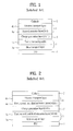
- FIG. 1 is a view showing construction of a conventional two-stack white organic light emitting device
- FIG. 2 is a view showing construction of another conventional two-stack white organic light emitting device
- FIG. 3 is a view showing construction of a conventional three-stack white organic light emitting device.
- the conventional white organic light emitting device has a structure in which a first stack 3, a charge generation layer 5, and a second stack 4 are stacked between an anode 1 and a cathode 2.
- the first stack 3 includes a hole transport layer 3a and a first emission layer 3b.
- the second stack 4 includes a second emission layer 4a and an electron transport layer 4b.
- the first emission layer 3b is a blue (B) emission layer and the second emission layer 4a is a yellow-green (YG) emission layer.
- the conventional white organic light emitting device has a structure in which a first stack 3, a charge generation layer 5, and a second stack 4 are stacked between an anode 1 and a cathode 2.
- the first stack 3 includes a hole transport layer 3a and three emission layers 3c.
- the second stack 4 includes three emission layers 4c and an electron transport layer 4b.
- the three emission layers 3c and 4c include blue (B), green (G), and red (R) emission layers.
- the conventional white organic light emitting device has a structure in which a first stack 3, a first charge generation layer 5, a second stack 4, a second charge generation layer 6, and a third stack 7 are stacked between an anode 1 and a cathode 2.
- the first stack 3 includes a hole transport layer 3a and a first emission layer 3b.
- the second stack 4 includes a second emission layer.
- the third stack 7 includes a third emission layer 7b and an electron transport layer 7a.
- the first emission layer 3b is a blue emission layer
- the second emission layer is a green emission layer
- the third emission layer 7b is a red emission layer.
- each charge generation layer is formed between the respective stacks to adjust charge balance between the respective stacks.
- the conventional white organic light emitting devices have the following problems.
- the conventional white organic light emitting devices shown in FIGs. 1 and 3 have similar characteristics. However, the conventional white organic light emitting device shown in FIG. 1 has a smaller number of layers and a smaller overall thickness than the conventional white organic light emitting device shown in FIG. 3 . Consequently, the conventional white organic light emitting device shown in FIG. 1 may have lower drive voltage and emit light having a white wavelength. Since it is necessary to cover three peaks using two peaks, however, in the conventional white organic light emitting device shown in FIG. 1 , luminance is low and power consumption is high due to a critical value of luminous efficiency provided by each emission layer when the white organic light emitting device is applied to a panel. In addition, in the conventional white organic light emitting device shown in FIG. 1 , a color viewing angle is limited due to each layer and an optical path based on a thickness corresponding thereto.
- each stack has low luminous efficiency and a short life span. Although the stacks are stacked, a color viewing angle is greatly limited and there are many color shifts.
- the present invention is directed to a white organic light emitting device that substantially obviates one or more problems due to limitations and disadvantages of the related art.
- An object of the present invention is to provide a white organic light emitting device including various emission layers, which is capable of providing a panel with improved luminous efficiency, an increased color viewing angle, and low power consumption.
- a white organic light emitting device includes at least two charge generation layers and at least three stacks between a first electrode and a second electrode, wherein the first stack includes an emission layer having a wavelength range of 440 to 470nm, the second stack includes an emission layer having a wavelength range of 530 to 570nm, and the third stack includes an emission layer having a wavelength range of 590 to 620nm and an emission layer having a wavelength range of 440 to 470nm.
- the at least three stacks may include 4 to 14 emission layers, at least two of the 4 to 14 emission layers may have different spectrums, and the 4 to 14 emission layers may include red, green, blue, yellow-green (YG), green-yellow, orange, and violet phosphorescent/fluorescent emission layers.
- the 4 to 14 emission layers may include red, green, blue, yellow-green (YG), green-yellow, orange, and violet phosphorescent/fluorescent emission layers.
- the stack most adjacent to the first electrode may include a blue emission layer.
- the white organic light emitting device may have a color temperature of 5500K to 13000K.
- a white organic light emitting device in another aspect of the present invention, includes a first stack, a first charge generation layer, a second stack, a second charge generation layer, and a third stack between a first electrode and a second electrode, wherein the first stack includes a blue zone emission layer, the second stack includes a yellow-green zone emission layer, and the third stack includes a red zone emission layer and a blue zone emission layer.
- the second stack may further include a green zone emission layer.
- a distance a between the blue (B) zone and the green (G) zone may be equal to or greater than a distance b between the green (G) zone and the red (R) zone (b ⁇ a).
- the yellow-green zone emission layer may have a full width at half maximum of 75nm or more.
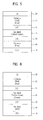
- FIG. 4 is a view schematically showing construction of a white organic light emitting device according to the present invention.
- the white organic light emitting device of the present invention includes at least two charge generation layers 30 and at least three stacks 40 between an anode 10 and a cathode 20.
- the first stack includes an emission layer having a wavelength range of 440 to 470nm
- the second stack includes an emission layer having a wavelength range of 530 to 570nm
- the third stack includes an emission layer having a wavelength range of 590 to 620nm and an emission layer having a wavelength range of 440 to 470nm.
- the 4 to 14 emission layers are provided. At least two of the 4 to 14 emission layers have different spectrums.
- the 4 to 14 emission layers include red, green, blue, yellow-green (YG), green-yellow, orange, and violet phosphorescent/fluorescent emission layers.
- the emission layer of the stack most adjacent to the anode 10 is a blue emission layer.
- the white organic light emitting device of the present invention has a color temperature of 5500K to 13000K.
- FIG. 5 is a view showing construction of a white organic light emitting device according to a first embodiment of the present invention.
- the white organic light emitting device includes a first stack 40, a first charge generation layer 30, a second stack 41, a second charge generation layer 31, and a third stack 42 between an anode 10 and a cathode 20.
- the anode 10 is formed of indium tin oxide (ITO) or indium zinc oxide (IZO).
- the cathode 20 is formed of a reflective metal material, such as aluminum (Al), gold (Au), molybdenum (Mo), chrome (Cr), copper (Cu), LiF, or an alloy of aluminum and LiF.
- the first and second charge generation layers (CGLs) 30 and 31 are formed between the stacks to adjust charge balance between the respective stacks.
- the first and second charge generation layers 30 and 31 each include an N type organic layer formed adjacent to the lower stack to inject electrons into the lower stack and a P type organic layer formed adjacent to the upper stack to inject holes into the upper stack.
- the first stack 40 includes an emission layer having a wavelength range of 440 to 470nm
- the second stack 41 includes an emission layer having a wavelength range of 530 to 570nm
- the third stack 42 includes an emission layer having a wavelength range of 590 to 620nm and an emission layer having a wavelength range of 440 to 470nm.
- Fluorescent blue is presently applied to products.
- the fluorescent blue has a theoretical luminous efficiency limiting value of about 13%.
- the first stack 40 includes only one blue zone emission layer.
- the second stack 41 includes only one yellow-green zone emission layer.
- the third stack 42 includes one red zone emission layer and one blue zone emission layer.
- a color temperature of a white organic light emitting device for displays is high, consumer appeal is also high. For this reason, one blue zone emission layer may be further added to increase the color temperature.
- red and blue zones are adjacent to each other in terms of thickness. When the red emission layer and the blue emission layer are disposed adjacent to each other as described above, it is possible to easily construct the white organic light emitting device.
- FIG. 6 is a view showing construction of a white organic light emitting device according to a second embodiment of the present invention.
- the white organic light emitting device includes a first stack 40, a first charge generation layer 30, a second stack 41, a second charge generation layer 31, and a third stack 42 between an anode 10 and a cathode 20.
- the anode 10 is formed of indium tin oxide (ITO) or indium zinc oxide (IZO).
- the cathode 20 is formed of a reflective metal material, such as aluminum (Al), gold (Au), molybdenum (Mo), chrome (Cr), copper (Cu), LiF, or an alloy of aluminum and LiF.
- the first and second charge generation layers (CGLs) 30 and 31 are formed between the stacks to adjust charge balance between the respective stacks.
- the first and second charge generation layers 30 and 31 each include an N type organic layer formed adjacent to the lower stack to inject electrons into the lower stack and a P type organic layer formed adjacent to the upper stack to inject holes into the upper stack.
- the first stack 40 includes an emission layer having a wavelength range of 440 to 470nm
- the second stack 41 includes two emission layers each having a wavelength range of 530 to 570nm
- the third stack 42 includes an emission layer having a wavelength range of 590 to 620nm and an emission layer having a wavelength range of 440 to 470nm.
- Fluorescent blue is presently applied to products.
- fluorescent blue has a theoretical luminous efficiency limiting value of about 13%.
- the first stack 40 includes only one blue zone emission layer.
- the second stack 41 includes two green zone emission layers.
- the green zone may be divided into green and yellow-green.
- a green zone emission layer and a yellow-green zone emission layer are used to alleviate sensitivity in green luminous efficiency which may be generated from the green zone depending upon the thickness of the device through the addition of the emission layer having the yellow-green wavelength.
- the third stack 42 includes one red zone emission layer and one blue zone emission layer.
- a color temperature of a white organic light emitting device for displays is high, consumer appeal is also high. For this reason, one blue zone emission layer may be further added to increase the color temperature.
- red and blue zones are adjacent to each other in terms of thickness. When the red emission layer and the blue emission layer are disposed adjacent to each other as described above, it is possible to easily construct the white organic light emitting device.
- luminous efficiency of the red zone emission layer may be lower than in a case in which only the red zone emission layer is used in the third stack.
- luminous efficiency of the red zone emission layer may be increased by the yellow-green zone emission layer used in the second stack 41 together with the green zone emission layer.
- the first stack 40 may include a hole injection layer adjacent to the anode 10
- the third stack 42 may include an electron injection layer adjacent to the cathode 20, and an electron transport layer and a hole transport layer may be formed on and under the emission layers of the first to third stacks.
- FIG. 7 is a graph showing comparison in characteristics of the white organic light emitting device between the first and second embodiments and a comparative example
- FIG. 8 is a table showing comparison in characteristics of the white organic light emitting device between the first and second embodiments and the comparative example.
- the white organic light emitting device includes a first stack 40, a first charge generation layer 30, a second stack 41, a second charge generation layer 31, and a third stack 42 between an anode 10 and a cathode 20 as in the first and second embodiments of the present invention.
- the first stack 40 includes only one blue zone emission layer
- the second stack 41 includes one yellow-green zone emission layer
- the third stack 42 includes one red zone emission layer.
- drive voltage Voled voltage applied to the panel during driving of white color
- a color viewing angle (a value indicating change of color coordinates measured at an angle of 60 degrees to the front of the panel) of the white organic light emitting device according to the first and second embodiments of the present invention is lower than that of the comparative example.
- panel efficiency efficiency of average luminance obtained during driving of various videos
- panel efficiency of the white organic light emitting device according to the first and second embodiments of the present invention is higher than that of the comparative example.
- each unit pixel may include four sub-pixels R, G, B, and W or three sub-pixels R, G, and B.
- the central peak of a photoluminescence (PL) wavelength of the phosphorescent yellow-green emission layer of the second stack is 556nm and full width at half maximum (FWHM) of the emission layer is 88nm.
- the central peak of the wavelength of the phosphorescent yellow-green emission layer may be moved or the FWHM of the emission layer may be adjusted to maximize panel efficiency.
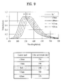
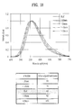
- FIG. 9 is a graph and a table showing spectrums of the phosphorescent yellow-green emission layer of the second stack according to the present invention when the PL central peak of the emission layer is moved -10nm, -20nm, +10nm, and +20nm and
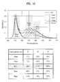
- FIG. 10 is a graph and a table showing panel efficiency of red (R), green (G), and blue (B) zones based on experimental results according to FIG. 9 .
- the PL central peak of the phosphorescent yellow-green emission layer is set to 540 to 570 nm.
- FIG. 11 is a graph and a table showing spectrums of the phosphorescent yellow-green emission layer of the second stack according to the present invention when FWHM of the emission layer is adjusted to a -10nm, -20nm, +10nm, and +20nm
- FIG. 12 is a graph and a table showing panel efficiency of red (R), green (G), and blue (B) zones based on experimental results according to FIG. 11 .
- FWHM of the yellow-green emission layer When FWHM of the yellow-green emission layer is increased as shown in FIG. 11 , satisfied results may be obtained as shown in FIG. 12 . That is, efficiency is lowered in the PL having FWHM less than reference. Consequently, FWHM of the yellow-green emission layer is set to 75nm or more.
- FIG. 13 is a graph showing distances between wavelengths based on a high-efficiency spectrum according to the present invention.
- the white organic light emitting device includes various emission layers. Consequently, drive voltage is lowered, a color viewing angle, which is a value indicating change of color coordinates measured at an angle of 60 degrees to the front of a panel, is improved, and average luminance (panel efficiency) obtained during driving of various videos is improved.
Landscapes
- Physics & Mathematics (AREA)
- Optics & Photonics (AREA)
- Electroluminescent Light Sources (AREA)
Abstract
Description
- This application claims the benefit of Korean Patent Application No. 10-
2013-0103154, filed on August 29, 2013 - The present invention relates to an organic light emitting device and, more particularly, to a white organic light emitting device including various emission layers with improved luminous efficiency, an increased color viewing angle, and low power consumption.
- Image display devices, which are core technology in information communication era, embodying various kinds of information on a screen have been developed such that the image display devices are thin, light, and portable and have high performance. An organic light emitting device (OLED) that controls a luminance amount of an organic emission layer to display an image has been spotlighted as a flat panel display device having smaller weight and volume than a cathode ray tube (CRT).
- An organic light emitting device, which is a self-emissive device having a thin emission layer disposed between two electrodes, may be configured to be thin as paper. Specifically, the organic light emitting device includes an anode, a hole injection layer (HIL), a hole transport layer (HTL), an emission layer, an electron transport layer (ETL), an electron injection layer (EIL), and a cathode.
- In recent years, active research has been conducted into a white organic light emitting device having a multi-layer structure (two stacks or more) in order to further improve luminous efficiency.
- That is, two or three stacks are provided and one emission layer is provided per stack to embody a white light emitting device. This white light emitting device may emit light having a white wavelength. When the white light emitting device is applied to a panel, however, luminance is low and power consumption is high due to a critical value of luminous efficiency provided by each emission layer.
- Alternatively, two or three stacks are provided and three emission layers are provided per stack to embody white spectrum. When this white light emitting device is applied to a panel, however, luminance is low and power consumption is high.
- Conventional organic light emitting devices will be described.
-
FIG. 1 is a view showing construction of a conventional two-stack white organic light emitting device,FIG. 2 is a view showing construction of another conventional two-stack white organic light emitting device, andFIG. 3 is a view showing construction of a conventional three-stack white organic light emitting device. - As shown in
FIG. 1 , the conventional white organic light emitting device has a structure in which afirst stack 3, acharge generation layer 5, and asecond stack 4 are stacked between ananode 1 and acathode 2. - The
first stack 3 includes ahole transport layer 3a and afirst emission layer 3b. Thesecond stack 4 includes asecond emission layer 4a and anelectron transport layer 4b. Thefirst emission layer 3b is a blue (B) emission layer and thesecond emission layer 4a is a yellow-green (YG) emission layer. - As shown in
FIG. 2 , the conventional white organic light emitting device has a structure in which afirst stack 3, acharge generation layer 5, and asecond stack 4 are stacked between ananode 1 and acathode 2. Thefirst stack 3 includes ahole transport layer 3a and threeemission layers 3c. Thesecond stack 4 includes threeemission layers 4c and anelectron transport layer 4b. The threeemission layers - As shown in
FIG. 3 , the conventional white organic light emitting device has a structure in which afirst stack 3, a firstcharge generation layer 5, asecond stack 4, a secondcharge generation layer 6, and athird stack 7 are stacked between ananode 1 and acathode 2. Thefirst stack 3 includes ahole transport layer 3a and afirst emission layer 3b. Thesecond stack 4 includes a second emission layer. Thethird stack 7 includes athird emission layer 7b and anelectron transport layer 7a. Thefirst emission layer 3b is a blue emission layer, the second emission layer is a green emission layer, and thethird emission layer 7b is a red emission layer. - In the conventional white organic light emitting devices, each charge generation layer is formed between the respective stacks to adjust charge balance between the respective stacks.
- However, the conventional white organic light emitting devices have the following problems.
- The conventional white organic light emitting devices shown in
FIGs. 1 and3 have similar characteristics. However, the conventional white organic light emitting device shown inFIG. 1 has a smaller number of layers and a smaller overall thickness than the conventional white organic light emitting device shown inFIG. 3 . Consequently, the conventional white organic light emitting device shown inFIG. 1 may have lower drive voltage and emit light having a white wavelength. Since it is necessary to cover three peaks using two peaks, however, in the conventional white organic light emitting device shown inFIG. 1 , luminance is low and power consumption is high due to a critical value of luminous efficiency provided by each emission layer when the white organic light emitting device is applied to a panel. In addition, in the conventional white organic light emitting device shown inFIG. 1 , a color viewing angle is limited due to each layer and an optical path based on a thickness corresponding thereto. - In the conventional white organic light emitting device shown in
FIG. 2 , each stack has low luminous efficiency and a short life span. Although the stacks are stacked, a color viewing angle is greatly limited and there are many color shifts. - Accordingly, the present invention is directed to a white organic light emitting device that substantially obviates one or more problems due to limitations and disadvantages of the related art.
- An object of the present invention is to provide a white organic light emitting device including various emission layers, which is capable of providing a panel with improved luminous efficiency, an increased color viewing angle, and low power consumption.
- Additional advantages, objects, and features of the invention will be set forth in part in the description which follows and in part will become apparent to those having ordinary skill in the art upon examination of the following or may be learned from practice of the invention. The objectives and other advantages of the invention may be realized and attained by the structure particularly pointed out in the written description and claims hereof as well as the appended drawings.
- To achieve these objects and other advantages and in accordance with the purpose of the invention, as embodied and broadly described herein, a white organic light emitting device includes at least two charge generation layers and at least three stacks between a first electrode and a second electrode, wherein the first stack includes an emission layer having a wavelength range of 440 to 470nm, the second stack includes an emission layer having a wavelength range of 530 to 570nm, and the third stack includes an emission layer having a wavelength range of 590 to 620nm and an emission layer having a wavelength range of 440 to 470nm.
- The at least three stacks may include 4 to 14 emission layers, at least two of the 4 to 14 emission layers may have different spectrums, and the 4 to 14 emission layers may include red, green, blue, yellow-green (YG), green-yellow, orange, and violet phosphorescent/fluorescent emission layers.
- The stack most adjacent to the first electrode may include a blue emission layer.
- The white organic light emitting device may have a color temperature of 5500K to 13000K.
- In another aspect of the present invention, a white organic light emitting device includes a first stack, a first charge generation layer, a second stack, a second charge generation layer, and a third stack between a first electrode and a second electrode, wherein the first stack includes a blue zone emission layer, the second stack includes a yellow-green zone emission layer, and the third stack includes a red zone emission layer and a blue zone emission layer.
- The second stack may further include a green zone emission layer.
- A distance a between the blue (B) zone and the green (G) zone may be equal to or greater than a distance b between the green (G) zone and the red (R) zone (b ≤a).
- The yellow-green zone emission layer may have a full width at half maximum of 75nm or more.
- It is to be understood that both the foregoing general description and the following detailed description of the present invention are exemplary and explanatory and are intended to provide further explanation of the invention as claimed.
- The accompanying drawings, which are included to provide a further understanding of the invention and are incorporated in and constitute a part of this application, illustrate embodiment(s) of the invention and together with the description serve to explain the principle of the invention. In the drawings:
-
FIG. 1 is a view showing construction of a conventional two-stack white organic light emitting device; -
FIG. 2 is a view showing construction of another conventional two-stack white organic light emitting device; -
FIG. 3 is a view showing construction of a conventional three-stack white organic light emitting device; -
FIG. 4 is a view schematically showing construction of a white organic light emitting device according to the present invention; -
FIG. 5 is a view showing construction of a white organic light emitting device according to a first embodiment of the present invention; -
FIG. 6 is a view showing construction of a white organic light emitting device according to a second embodiment of the present invention; -
FIG. 7 is a graph showing comparison in characteristics of the white organic light emitting device between the first and second embodiments and a comparative example; -
FIG. 8 is a table showing comparison in characteristics of the white organic light emitting device between the first and second embodiments and the comparative example; -
FIG. 9 is a graph and a table showing spectrums of a phosphorescent yellow-green emission layer of a second stack according to the present invention when a photoluminescence (PL) central peak of the emission layer is moved -10nm, -20nm, +10nm, and +20nm; -
FIG. 10 is a graph and a table showing panel efficiency of red (R), green (G), and blue (B) zones based on experimental results according toFIG. 9 ; -
FIG. 11 is a graph and a table showing spectrums of the phosphorescent yellow-green emission layer of the second stack according to the present invention when full width at half maximum (FWHM) of the emission layer is adjusted to a -10nm, -20nm, +10nm, and +20nm; -
FIG. 12 is a graph and a table showing panel efficiency of red (R), green (G), and blue (B) zones based on experimental results according toFIG. 11 ; and -
FIG. 13 is a graph showing distances between wavelengths based on a high-efficiency spectrum according to the present invention. - Reference will now be made in detail to the preferred embodiments of the present invention, examples of which are illustrated in the accompanying drawings. Wherever possible, the same reference numbers will be used throughout the drawings to refer to the same or like parts.
-
FIG. 4 is a view schematically showing construction of a white organic light emitting device according to the present invention. - As shown in
FIG. 4 , the white organic light emitting device of the present invention includes at least two charge generation layers 30 and at least threestacks 40 between ananode 10 and acathode 20. - The first stack includes an emission layer having a wavelength range of 440 to 470nm, the second stack includes an emission layer having a wavelength range of 530 to 570nm, and the third stack includes an emission layer having a wavelength range of 590 to 620nm and an emission layer having a wavelength range of 440 to 470nm.
- 4 to 14 emission layers are provided. At least two of the 4 to 14 emission layers have different spectrums. The 4 to 14 emission layers include red, green, blue, yellow-green (YG), green-yellow, orange, and violet phosphorescent/fluorescent emission layers.
- The emission layer of the stack most adjacent to the
anode 10 is a blue emission layer. The white organic light emitting device of the present invention has a color temperature of 5500K to 13000K. - A first embodiment of the white organic light emitting device with the above-stated construction will be described.
-
FIG. 5 is a view showing construction of a white organic light emitting device according to a first embodiment of the present invention. - As shown in
FIG. 5 , the white organic light emitting device according to a first embodiment of the present invention includes afirst stack 40, a firstcharge generation layer 30, asecond stack 41, a secondcharge generation layer 31, and athird stack 42 between ananode 10 and acathode 20. - The
anode 10 is formed of indium tin oxide (ITO) or indium zinc oxide (IZO). Thecathode 20 is formed of a reflective metal material, such as aluminum (Al), gold (Au), molybdenum (Mo), chrome (Cr), copper (Cu), LiF, or an alloy of aluminum and LiF. - The first and second charge generation layers (CGLs) 30 and 31 are formed between the stacks to adjust charge balance between the respective stacks. Although not shown, the first and second charge generation layers 30 and 31 each include an N type organic layer formed adjacent to the lower stack to inject electrons into the lower stack and a P type organic layer formed adjacent to the upper stack to inject holes into the upper stack.
- The
first stack 40 includes an emission layer having a wavelength range of 440 to 470nm, thesecond stack 41 includes an emission layer having a wavelength range of 530 to 570nm, and thethird stack 42 includes an emission layer having a wavelength range of 590 to 620nm and an emission layer having a wavelength range of 440 to 470nm. - Fluorescent blue is presently applied to products. However, the fluorescent blue has a theoretical luminous efficiency limiting value of about 13%. As a result, it is difficult to embody a high-performance white organic light emitting device. For this reason, the
first stack 40 includes only one blue zone emission layer. - The
second stack 41 includes only one yellow-green zone emission layer. - The
third stack 42 includes one red zone emission layer and one blue zone emission layer. When a color temperature of a white organic light emitting device for displays is high, consumer appeal is also high. For this reason, one blue zone emission layer may be further added to increase the color temperature. In addition, in most optical cavities, red and blue zones are adjacent to each other in terms of thickness. When the red emission layer and the blue emission layer are disposed adjacent to each other as described above, it is possible to easily construct the white organic light emitting device. -
FIG. 6 is a view showing construction of a white organic light emitting device according to a second embodiment of the present invention. - As shown in
FIG. 6 , the white organic light emitting device includes afirst stack 40, a firstcharge generation layer 30, asecond stack 41, a secondcharge generation layer 31, and athird stack 42 between ananode 10 and acathode 20. - The
anode 10 is formed of indium tin oxide (ITO) or indium zinc oxide (IZO). Thecathode 20 is formed of a reflective metal material, such as aluminum (Al), gold (Au), molybdenum (Mo), chrome (Cr), copper (Cu), LiF, or an alloy of aluminum and LiF. - The first and second charge generation layers (CGLs) 30 and 31 are formed between the stacks to adjust charge balance between the respective stacks. Although not shown, the first and second charge generation layers 30 and 31 each include an N type organic layer formed adjacent to the lower stack to inject electrons into the lower stack and a P type organic layer formed adjacent to the upper stack to inject holes into the upper stack.
- The
first stack 40 includes an emission layer having a wavelength range of 440 to 470nm, thesecond stack 41 includes two emission layers each having a wavelength range of 530 to 570nm, and thethird stack 42 includes an emission layer having a wavelength range of 590 to 620nm and an emission layer having a wavelength range of 440 to 470nm. - Fluorescent blue is presently applied to products. However, fluorescent blue has a theoretical luminous efficiency limiting value of about 13%. As a result, it is difficult to embody a high-performance white organic light emitting device. For this reason, the
first stack 40 includes only one blue zone emission layer. - The
second stack 41 includes two green zone emission layers. The green zone may be divided into green and yellow-green. A green zone emission layer and a yellow-green zone emission layer are used to alleviate sensitivity in green luminous efficiency which may be generated from the green zone depending upon the thickness of the device through the addition of the emission layer having the yellow-green wavelength. - The
third stack 42 includes one red zone emission layer and one blue zone emission layer. When a color temperature of a white organic light emitting device for displays is high, consumer appeal is also high. For this reason, one blue zone emission layer may be further added to increase the color temperature. In addition, in most optical cavities, red and blue zones are adjacent to each other in terms of thickness. When the red emission layer and the blue emission layer are disposed adjacent to each other as described above, it is possible to easily construct the white organic light emitting device. - In a case in which the red zone emission layer and the blue zone emission layer are used in the third stack, luminous efficiency of the red zone emission layer may be lower than in a case in which only the red zone emission layer is used in the third stack. However, luminous efficiency of the red zone emission layer may be increased by the yellow-green zone emission layer used in the
second stack 41 together with the green zone emission layer. - Although not shown, in the white organic light emitting device according to the first and second embodiments of the present invention, the
first stack 40 may include a hole injection layer adjacent to theanode 10, thethird stack 42 may include an electron injection layer adjacent to thecathode 20, and an electron transport layer and a hole transport layer may be formed on and under the emission layers of the first to third stacks. -
FIG. 7 is a graph showing comparison in characteristics of the white organic light emitting device between the first and second embodiments and a comparative example andFIG. 8 is a table showing comparison in characteristics of the white organic light emitting device between the first and second embodiments and the comparative example. - The white organic light emitting device according to the comparative example includes a
first stack 40, a firstcharge generation layer 30, asecond stack 41, a secondcharge generation layer 31, and athird stack 42 between ananode 10 and acathode 20 as in the first and second embodiments of the present invention. However, thefirst stack 40 includes only one blue zone emission layer, thesecond stack 41 includes one yellow-green zone emission layer, and thethird stack 42 includes one red zone emission layer. - As shown in
FIG. 8 , when the white organic light emitting device according to the first and second embodiments of the present invention is applied to a panel, drive voltage Voled (voltage applied to the panel during driving of white color) of the white organic light emitting device according to the first and second embodiments of the present invention is lower than that of the comparative example. - In addition, a color viewing angle (a value indicating change of color coordinates measured at an angle of 60 degrees to the front of the panel) of the white organic light emitting device according to the first and second embodiments of the present invention is lower than that of the comparative example.
- Furthermore, panel efficiency (efficiency of average luminance obtained during driving of various videos) of the white organic light emitting device according to the first and second embodiments of the present invention is higher than that of the comparative example.
- When the white organic light emitting device according to each embodiment of the present invention is applied to a panel, each unit pixel may include four sub-pixels R, G, B, and W or three sub-pixels R, G, and B.
- Meanwhile, in a three-stack, three-peak structure as in the white organic light emitting device according to the first embodiment of the present invention, the central peak of a photoluminescence (PL) wavelength of the phosphorescent yellow-green emission layer of the second stack is 556nm and full width at half maximum (FWHM) of the emission layer is 88nm. The central peak of the wavelength of the phosphorescent yellow-green emission layer may be moved or the FWHM of the emission layer may be adjusted to maximize panel efficiency.
-
FIG. 9 is a graph and a table showing spectrums of the phosphorescent yellow-green emission layer of the second stack according to the present invention when the PL central peak of the emission layer is moved -10nm, -20nm, +10nm, and +20nm andFIG. 10 is a graph and a table showing panel efficiency of red (R), green (G), and blue (B) zones based on experimental results according toFIG. 9 . - When the PL central peak of the phosphorescent yellow-green emission layer is moved to short wavelength sides (-10nm and -20nm) as shown in
FIG. 9 , the red (R) zone is insufficient as shown inFIG. 10 . On the other hand, when the PL central peak of the phosphorescent yellow-green emission layer is moved to long wavelength sides (+10nm and +10nm) as shown inFIG. 9 , the green (G) zone is insufficient as shown inFIG. 10 . Consequently, the PL central peak of the phosphorescent yellow-green emission layer is set to 540 to 570 nm. -
FIG. 11 is a graph and a table showing spectrums of the phosphorescent yellow-green emission layer of the second stack according to the present invention when FWHM of the emission layer is adjusted to a -10nm, -20nm, +10nm, and +20nm andFIG. 12 is a graph and a table showing panel efficiency of red (R), green (G), and blue (B) zones based on experimental results according toFIG. 11 . - When FWHM of the yellow-green emission layer is increased as shown in
FIG. 11 , satisfied results may be obtained as shown inFIG. 12 . That is, efficiency is lowered in the PL having FWHM less than reference. Consequently, FWHM of the yellow-green emission layer is set to 75nm or more. -
FIG. 13 is a graph showing distances between wavelengths based on a high-efficiency spectrum according to the present invention. - As shown in
FIG. 13 , overall efficiency is optimized when a distance a between the blue (B) zone and the green (G) zone is equal to or greater than a distance b between the green (G) zone and the red (R) zone (b ≤a). - As is apparent from the above description, the white organic light emitting device according to the present invention includes various emission layers. Consequently, drive voltage is lowered, a color viewing angle, which is a value indicating change of color coordinates measured at an angle of 60 degrees to the front of a panel, is improved, and average luminance (panel efficiency) obtained during driving of various videos is improved.
- It will be apparent to those skilled in the art that various modifications and variations can be made in the present invention without departing from the spirit or scope of the inventions. Thus, it is intended that the present invention covers the modifications and variations of this invention provided they come within the scope of the appended claims and their equivalents.
Claims (8)
- A white organic light emitting device comprising:at least two charge generation layers and at least three stacks between a first electrode and a second electrode, whereinthe first stack comprises an emission layer having a wavelength range of 440 to 470nm, the second stack comprises an emission layer having a wavelength range of 530 to 570nm, and the third stack comprises an emission layer having a wavelength range of 590 to 620nm and an emission layer having a wavelength range of 440 to 470nm.
- The white organic light emitting device according to claim 1, wherein the at least three stacks comprises 4 to 14 emission layers, at least two of the 4 to 14 emission layers have different spectrums, and the 4 to 14 emission layers comprise red, green, blue, yellow-green (YG), green-yellow, orange, and violet phosphorescent/fluorescent emission layers.
- The white organic light emitting device according to claim 1 or 2, wherein the stack most adjacent to the first electrode comprises a blue emission layer.
- The white organic light emitting device according to any of claims 1 to 3, wherein the white organic light emitting device has a color temperature of 5500K to 13000K.
- A white organic light emitting device comprising:a first stack, a first charge generation layer, a second stack, a second charge generation layer, and a third stack between a first electrode and a second electrode, whereinthe first stack comprises a blue zone emission layer, the second stack comprises a yellow-green zone emission layer, and the third stack comprises a red zone emission layer and a blue zone emission layer.
- The white organic light emitting device according to claim 5, wherein the second stack further comprises a green zone emission layer.
- The white organic light emitting device according to claim 5 or 6, wherein a distance a between the blue (B) zone and the green (G) zone is equal to or greater than a distance b between the green (G) zone and the red (R) zone.
- The white organic light emitting device according to any of claims 5 to 7, wherein the yellow-green zone emission layer has a full width at half maximum of 75nm or more.
Applications Claiming Priority (1)
| Application Number | Priority Date | Filing Date | Title |
|---|---|---|---|
| KR1020130103154A KR102081117B1 (en) | 2013-08-29 | 2013-08-29 | White organic light emitting device |
Publications (2)
| Publication Number | Publication Date |
|---|---|
| EP2846372A1 true EP2846372A1 (en) | 2015-03-11 |
| EP2846372B1 EP2846372B1 (en) | 2016-09-21 |
Family
ID=50828809
Family Applications (1)
| Application Number | Title | Priority Date | Filing Date |
|---|---|---|---|
| EP14179930.4A Active EP2846372B1 (en) | 2013-08-29 | 2014-08-05 | White organic light emitting device |
Country Status (4)
| Country | Link |
|---|---|
| US (1) | US9786861B2 (en) |
| EP (1) | EP2846372B1 (en) |
| KR (1) | KR102081117B1 (en) |
| CN (1) | CN104425736B (en) |
Cited By (2)
| Publication number | Priority date | Publication date | Assignee | Title |
|---|---|---|---|---|
| EP2950362A1 (en) * | 2014-05-26 | 2015-12-02 | LG Display Co., Ltd. | White organic light emitting device |
| JP2020524391A (en) * | 2017-06-20 | 2020-08-13 | 京東方科技集團股▲ふん▼有限公司Boe Technology Group Co.,Ltd. | Organic light emitting diode display panel, manufacturing method thereof, and display device |
Families Citing this family (15)
| Publication number | Priority date | Publication date | Assignee | Title |
|---|---|---|---|---|
| KR102224743B1 (en) | 2014-10-21 | 2021-03-09 | 삼성디스플레이 주식회사 | Stretchable organic light emitting display apparatus |
| US9859529B2 (en) * | 2014-11-13 | 2018-01-02 | Lg Display Co., Ltd. | Organic light emitting display device |
| US11145837B2 (en) * | 2014-12-17 | 2021-10-12 | Universal Display Corporation | Color stable organic light emitting diode stack |
| JP6022014B2 (en) * | 2015-03-02 | 2016-11-09 | Lumiotec株式会社 | Organic electroluminescent device and lighting device |
| KR102377466B1 (en) * | 2015-10-29 | 2022-03-21 | 엘지디스플레이 주식회사 | Organic light emitting display apparatus |
| KR102715632B1 (en) | 2016-09-27 | 2024-10-11 | 삼성디스플레이 주식회사 | Organic electroluminescence display device |
| CN106531775A (en) | 2016-12-30 | 2017-03-22 | 京东方科技集团股份有限公司 | Organic light-emitting diode display substrate and display device and preparation method thereof |
| KR102367821B1 (en) * | 2017-10-31 | 2022-02-28 | 엘지디스플레이 주식회사 | White Organic Light Emitting Device and Organic Light Emitting Display Device |
| JP6961109B2 (en) * | 2019-01-15 | 2021-11-05 | ソニーセミコンダクタソリューションズ株式会社 | Display devices, manufacturing methods for display devices, and electronic devices |
| US10826010B1 (en) | 2019-06-20 | 2020-11-03 | Sharp Kabushiki Kaisha | High-efficiency QLED structures |
| US10930888B2 (en) | 2019-07-22 | 2021-02-23 | Sharp Kabushiki Kaisha | High-efficiency QLED structures |
| US11316135B2 (en) | 2019-07-22 | 2022-04-26 | Sharp Kabushiki Kaisha | High-efficiency QLED structures |
| US12588382B2 (en) | 2019-07-29 | 2026-03-24 | Universal Display Corporation | Color stable multicolor OLED device structures |
| KR102845493B1 (en) * | 2021-04-05 | 2025-08-13 | 삼성디스플레이 주식회사 | Light emitting device and display apparatus including the same |
| CN115295596B (en) * | 2022-08-19 | 2023-05-09 | 昆山国显光电有限公司 | Display panel and display device |
Citations (4)
| Publication number | Priority date | Publication date | Assignee | Title |
|---|---|---|---|---|
| WO2006130883A2 (en) * | 2005-06-01 | 2006-12-07 | The Trustees Of Princeton University | Fluorescent filtered electrophosphorescence |
| US20070278937A1 (en) * | 2006-06-05 | 2007-12-06 | Stephen Forrest | Organic light-emitting device with a phosphor-sensitized fluorescent emission layer |
| US20100288362A1 (en) * | 2009-05-13 | 2010-11-18 | Hatwar Tukaram K | Internal connector for organic electronic devices |
| WO2012141107A1 (en) * | 2011-04-14 | 2012-10-18 | 株式会社日立製作所 | Organic light-emitting device and light source device using same |
Family Cites Families (8)
| Publication number | Priority date | Publication date | Assignee | Title |
|---|---|---|---|---|
| KR101316752B1 (en) * | 2007-05-31 | 2013-10-08 | 삼성디스플레이 주식회사 | White organic light emitting display |
| US7977872B2 (en) * | 2008-09-16 | 2011-07-12 | Global Oled Technology Llc | High-color-temperature tandem white OLED |
| JP6108664B2 (en) * | 2011-04-04 | 2017-04-05 | ローム株式会社 | Organic EL device |
| US10079349B2 (en) * | 2011-05-27 | 2018-09-18 | Universal Display Corporation | Organic electroluminescent materials and devices |
| KR101429924B1 (en) * | 2011-12-08 | 2014-08-14 | 엘지디스플레이 주식회사 | Tandem White Organic Emitting Device |
| KR101535824B1 (en) * | 2011-12-16 | 2015-07-13 | 엘지디스플레이 주식회사 | Organic Light Emitting Device |
| KR101400058B1 (en) * | 2011-12-23 | 2014-05-30 | 엘지디스플레이 주식회사 | Organic Light Emitting Display Device |
| KR102081605B1 (en) * | 2013-07-31 | 2020-02-27 | 엘지디스플레이 주식회사 | White organic light emitting diode device |
-
2013
- 2013-08-29 KR KR1020130103154A patent/KR102081117B1/en active Active
-
2014
- 2014-06-23 CN CN201410283092.9A patent/CN104425736B/en active Active
- 2014-08-05 EP EP14179930.4A patent/EP2846372B1/en active Active
- 2014-08-21 US US14/465,299 patent/US9786861B2/en active Active
Patent Citations (4)
| Publication number | Priority date | Publication date | Assignee | Title |
|---|---|---|---|---|
| WO2006130883A2 (en) * | 2005-06-01 | 2006-12-07 | The Trustees Of Princeton University | Fluorescent filtered electrophosphorescence |
| US20070278937A1 (en) * | 2006-06-05 | 2007-12-06 | Stephen Forrest | Organic light-emitting device with a phosphor-sensitized fluorescent emission layer |
| US20100288362A1 (en) * | 2009-05-13 | 2010-11-18 | Hatwar Tukaram K | Internal connector for organic electronic devices |
| WO2012141107A1 (en) * | 2011-04-14 | 2012-10-18 | 株式会社日立製作所 | Organic light-emitting device and light source device using same |
Cited By (6)
| Publication number | Priority date | Publication date | Assignee | Title |
|---|---|---|---|---|
| EP2950362A1 (en) * | 2014-05-26 | 2015-12-02 | LG Display Co., Ltd. | White organic light emitting device |
| US9705102B2 (en) | 2014-05-26 | 2017-07-11 | Lg Display Co., Ltd. | White organic light emitting device |
| US10038157B2 (en) | 2014-05-26 | 2018-07-31 | Lg Display Co., Ltd. | White organic light emitting device |
| JP2020524391A (en) * | 2017-06-20 | 2020-08-13 | 京東方科技集團股▲ふん▼有限公司Boe Technology Group Co.,Ltd. | Organic light emitting diode display panel, manufacturing method thereof, and display device |
| EP3644368A4 (en) * | 2017-06-20 | 2021-03-17 | BOE Technology Group Co., Ltd. | ORGANIC LUMINESCENT DIODES DISPLAY PANEL AND METHOD FOR MANUFACTURING THE SAME, AND DISPLAY DEVICE |
| US11189811B2 (en) | 2017-06-20 | 2021-11-30 | Boe Technology Group Co., Ltd. | Organic light emitting diode display panel having wide color gamut and low power consumption, manufacturing method thereof, and display device |
Also Published As
| Publication number | Publication date |
|---|---|
| KR102081117B1 (en) | 2020-02-25 |
| US9786861B2 (en) | 2017-10-10 |
| EP2846372B1 (en) | 2016-09-21 |
| US20150060812A1 (en) | 2015-03-05 |
| KR20150025417A (en) | 2015-03-10 |
| CN104425736A (en) | 2015-03-18 |
| CN104425736B (en) | 2017-07-14 |
Similar Documents
| Publication | Publication Date | Title |
|---|---|---|
| EP2846372B1 (en) | White organic light emitting device | |
| US10741781B2 (en) | White organic light emitting device | |
| KR102277563B1 (en) | White organic light emitting device | |
| US9831291B2 (en) | Organic light emitting display device and method of manufacturing the same | |
| US9425422B2 (en) | Organic light emitting display device | |
| US9159957B2 (en) | White organic light emitting device | |
| CN102881833B (en) | Organic light emitting diode | |
| US10157966B2 (en) | Organic light emitting display device | |
| CN104752623B (en) | Organnic electroluminescent device and organic electroluminescence display device and method of manufacturing same | |
| CN104103765B (en) | Oled device | |
| KR20120077301A (en) | White organic light emitting device | |
| CN105609648A (en) | Organic light emitting diode and organic light emitting diode display | |
| US9799844B2 (en) | Organic light emitting element | |
| KR102089331B1 (en) | Organic light emitting display | |
| KR20170112894A (en) | Organic light emitting display device | |
| KR20130077016A (en) | White organic light emitting display device | |
| KR20120076255A (en) | White organic light emitting device | |
| CN120787082A (en) | Display panel and display device |
Legal Events
| Date | Code | Title | Description |
|---|---|---|---|
| 17P | Request for examination filed |
Effective date: 20140805 |
|
| AK | Designated contracting states |
Kind code of ref document: A1 Designated state(s): AL AT BE BG CH CY CZ DE DK EE ES FI FR GB GR HR HU IE IS IT LI LT LU LV MC MK MT NL NO PL PT RO RS SE SI SK SM TR |
|
| AX | Request for extension of the european patent |
Extension state: BA ME |
|
| PUAI | Public reference made under article 153(3) epc to a published international application that has entered the european phase |
Free format text: ORIGINAL CODE: 0009012 |
|
| 17Q | First examination report despatched |
Effective date: 20150903 |
|
| GRAP | Despatch of communication of intention to grant a patent |
Free format text: ORIGINAL CODE: EPIDOSNIGR1 |
|
| INTG | Intention to grant announced |
Effective date: 20160407 |
|
| GRAS | Grant fee paid |
Free format text: ORIGINAL CODE: EPIDOSNIGR3 |
|
| GRAA | (expected) grant |
Free format text: ORIGINAL CODE: 0009210 |
|
| AK | Designated contracting states |
Kind code of ref document: B1 Designated state(s): AL AT BE BG CH CY CZ DE DK EE ES FI FR GB GR HR HU IE IS IT LI LT LU LV MC MK MT NL NO PL PT RO RS SE SI SK SM TR |
|
| REG | Reference to a national code |
Ref country code: GB Ref legal event code: FG4D |
|
| REG | Reference to a national code |
Ref country code: CH Ref legal event code: EP |
|
| REG | Reference to a national code |
Ref country code: AT Ref legal event code: REF Ref document number: 831669 Country of ref document: AT Kind code of ref document: T Effective date: 20161015 |
|
| REG | Reference to a national code |
Ref country code: IE Ref legal event code: FG4D |
|
| REG | Reference to a national code |
Ref country code: DE Ref legal event code: R096 Ref document number: 602014003779 Country of ref document: DE |
|
| REG | Reference to a national code |
Ref country code: LT Ref legal event code: MG4D Ref country code: NL Ref legal event code: MP Effective date: 20160921 |
|
| PG25 | Lapsed in a contracting state [announced via postgrant information from national office to epo] |
Ref country code: NO Free format text: LAPSE BECAUSE OF FAILURE TO SUBMIT A TRANSLATION OF THE DESCRIPTION OR TO PAY THE FEE WITHIN THE PRESCRIBED TIME-LIMIT Effective date: 20161221 Ref country code: FI Free format text: LAPSE BECAUSE OF FAILURE TO SUBMIT A TRANSLATION OF THE DESCRIPTION OR TO PAY THE FEE WITHIN THE PRESCRIBED TIME-LIMIT Effective date: 20160921 Ref country code: RS Free format text: LAPSE BECAUSE OF FAILURE TO SUBMIT A TRANSLATION OF THE DESCRIPTION OR TO PAY THE FEE WITHIN THE PRESCRIBED TIME-LIMIT Effective date: 20160921 Ref country code: LT Free format text: LAPSE BECAUSE OF FAILURE TO SUBMIT A TRANSLATION OF THE DESCRIPTION OR TO PAY THE FEE WITHIN THE PRESCRIBED TIME-LIMIT Effective date: 20160921 |
|
| REG | Reference to a national code |
Ref country code: AT Ref legal event code: MK05 Ref document number: 831669 Country of ref document: AT Kind code of ref document: T Effective date: 20160921 |
|
| PG25 | Lapsed in a contracting state [announced via postgrant information from national office to epo] |
Ref country code: NL Free format text: LAPSE BECAUSE OF FAILURE TO SUBMIT A TRANSLATION OF THE DESCRIPTION OR TO PAY THE FEE WITHIN THE PRESCRIBED TIME-LIMIT Effective date: 20160921 Ref country code: GR Free format text: LAPSE BECAUSE OF FAILURE TO SUBMIT A TRANSLATION OF THE DESCRIPTION OR TO PAY THE FEE WITHIN THE PRESCRIBED TIME-LIMIT Effective date: 20161222 Ref country code: LV Free format text: LAPSE BECAUSE OF FAILURE TO SUBMIT A TRANSLATION OF THE DESCRIPTION OR TO PAY THE FEE WITHIN THE PRESCRIBED TIME-LIMIT Effective date: 20160921 Ref country code: SE Free format text: LAPSE BECAUSE OF FAILURE TO SUBMIT A TRANSLATION OF THE DESCRIPTION OR TO PAY THE FEE WITHIN THE PRESCRIBED TIME-LIMIT Effective date: 20160921 |
|
| PG25 | Lapsed in a contracting state [announced via postgrant information from national office to epo] |
Ref country code: RO Free format text: LAPSE BECAUSE OF FAILURE TO SUBMIT A TRANSLATION OF THE DESCRIPTION OR TO PAY THE FEE WITHIN THE PRESCRIBED TIME-LIMIT Effective date: 20160921 Ref country code: EE Free format text: LAPSE BECAUSE OF FAILURE TO SUBMIT A TRANSLATION OF THE DESCRIPTION OR TO PAY THE FEE WITHIN THE PRESCRIBED TIME-LIMIT Effective date: 20160921 |
|
| PG25 | Lapsed in a contracting state [announced via postgrant information from national office to epo] |
Ref country code: CZ Free format text: LAPSE BECAUSE OF FAILURE TO SUBMIT A TRANSLATION OF THE DESCRIPTION OR TO PAY THE FEE WITHIN THE PRESCRIBED TIME-LIMIT Effective date: 20160921 Ref country code: IS Free format text: LAPSE BECAUSE OF FAILURE TO SUBMIT A TRANSLATION OF THE DESCRIPTION OR TO PAY THE FEE WITHIN THE PRESCRIBED TIME-LIMIT Effective date: 20170121 Ref country code: PT Free format text: LAPSE BECAUSE OF FAILURE TO SUBMIT A TRANSLATION OF THE DESCRIPTION OR TO PAY THE FEE WITHIN THE PRESCRIBED TIME-LIMIT Effective date: 20170123 Ref country code: SM Free format text: LAPSE BECAUSE OF FAILURE TO SUBMIT A TRANSLATION OF THE DESCRIPTION OR TO PAY THE FEE WITHIN THE PRESCRIBED TIME-LIMIT Effective date: 20160921 Ref country code: AT Free format text: LAPSE BECAUSE OF FAILURE TO SUBMIT A TRANSLATION OF THE DESCRIPTION OR TO PAY THE FEE WITHIN THE PRESCRIBED TIME-LIMIT Effective date: 20160921 Ref country code: ES Free format text: LAPSE BECAUSE OF FAILURE TO SUBMIT A TRANSLATION OF THE DESCRIPTION OR TO PAY THE FEE WITHIN THE PRESCRIBED TIME-LIMIT Effective date: 20160921 Ref country code: BG Free format text: LAPSE BECAUSE OF FAILURE TO SUBMIT A TRANSLATION OF THE DESCRIPTION OR TO PAY THE FEE WITHIN THE PRESCRIBED TIME-LIMIT Effective date: 20161221 Ref country code: SK Free format text: LAPSE BECAUSE OF FAILURE TO SUBMIT A TRANSLATION OF THE DESCRIPTION OR TO PAY THE FEE WITHIN THE PRESCRIBED TIME-LIMIT Effective date: 20160921 Ref country code: PL Free format text: LAPSE BECAUSE OF FAILURE TO SUBMIT A TRANSLATION OF THE DESCRIPTION OR TO PAY THE FEE WITHIN THE PRESCRIBED TIME-LIMIT Effective date: 20160921 Ref country code: BE Free format text: LAPSE BECAUSE OF FAILURE TO SUBMIT A TRANSLATION OF THE DESCRIPTION OR TO PAY THE FEE WITHIN THE PRESCRIBED TIME-LIMIT Effective date: 20160921 |
|
| REG | Reference to a national code |
Ref country code: DE Ref legal event code: R097 Ref document number: 602014003779 Country of ref document: DE |
|
| PG25 | Lapsed in a contracting state [announced via postgrant information from national office to epo] |
Ref country code: IT Free format text: LAPSE BECAUSE OF FAILURE TO SUBMIT A TRANSLATION OF THE DESCRIPTION OR TO PAY THE FEE WITHIN THE PRESCRIBED TIME-LIMIT Effective date: 20160921 |
|
| REG | Reference to a national code |
Ref country code: FR Ref legal event code: PLFP Year of fee payment: 4 |
|
| PLBE | No opposition filed within time limit |
Free format text: ORIGINAL CODE: 0009261 |
|
| STAA | Information on the status of an ep patent application or granted ep patent |
Free format text: STATUS: NO OPPOSITION FILED WITHIN TIME LIMIT |
|
| PG25 | Lapsed in a contracting state [announced via postgrant information from national office to epo] |
Ref country code: DK Free format text: LAPSE BECAUSE OF FAILURE TO SUBMIT A TRANSLATION OF THE DESCRIPTION OR TO PAY THE FEE WITHIN THE PRESCRIBED TIME-LIMIT Effective date: 20160921 |
|
| 26N | No opposition filed |
Effective date: 20170622 |
|
| PG25 | Lapsed in a contracting state [announced via postgrant information from national office to epo] |
Ref country code: SI Free format text: LAPSE BECAUSE OF FAILURE TO SUBMIT A TRANSLATION OF THE DESCRIPTION OR TO PAY THE FEE WITHIN THE PRESCRIBED TIME-LIMIT Effective date: 20160921 |
|
| REG | Reference to a national code |
Ref country code: CH Ref legal event code: PL |
|
| PG25 | Lapsed in a contracting state [announced via postgrant information from national office to epo] |
Ref country code: MC Free format text: LAPSE BECAUSE OF FAILURE TO SUBMIT A TRANSLATION OF THE DESCRIPTION OR TO PAY THE FEE WITHIN THE PRESCRIBED TIME-LIMIT Effective date: 20160921 |
|
| PG25 | Lapsed in a contracting state [announced via postgrant information from national office to epo] |
Ref country code: CH Free format text: LAPSE BECAUSE OF NON-PAYMENT OF DUE FEES Effective date: 20170831 Ref country code: LI Free format text: LAPSE BECAUSE OF NON-PAYMENT OF DUE FEES Effective date: 20170831 |
|
| REG | Reference to a national code |
Ref country code: IE Ref legal event code: MM4A |
|
| REG | Reference to a national code |
Ref country code: FR Ref legal event code: PLFP Year of fee payment: 5 |
|
| PG25 | Lapsed in a contracting state [announced via postgrant information from national office to epo] |
Ref country code: LU Free format text: LAPSE BECAUSE OF NON-PAYMENT OF DUE FEES Effective date: 20170805 |
|
| PG25 | Lapsed in a contracting state [announced via postgrant information from national office to epo] |
Ref country code: IE Free format text: LAPSE BECAUSE OF NON-PAYMENT OF DUE FEES Effective date: 20170805 |
|
| PG25 | Lapsed in a contracting state [announced via postgrant information from national office to epo] |
Ref country code: MT Free format text: LAPSE BECAUSE OF NON-PAYMENT OF DUE FEES Effective date: 20170805 |
|
| PG25 | Lapsed in a contracting state [announced via postgrant information from national office to epo] |
Ref country code: AL Free format text: LAPSE BECAUSE OF FAILURE TO SUBMIT A TRANSLATION OF THE DESCRIPTION OR TO PAY THE FEE WITHIN THE PRESCRIBED TIME-LIMIT Effective date: 20160921 |
|
| PG25 | Lapsed in a contracting state [announced via postgrant information from national office to epo] |
Ref country code: HU Free format text: LAPSE BECAUSE OF FAILURE TO SUBMIT A TRANSLATION OF THE DESCRIPTION OR TO PAY THE FEE WITHIN THE PRESCRIBED TIME-LIMIT; INVALID AB INITIO Effective date: 20140805 |
|
| PG25 | Lapsed in a contracting state [announced via postgrant information from national office to epo] |
Ref country code: CY Free format text: LAPSE BECAUSE OF FAILURE TO SUBMIT A TRANSLATION OF THE DESCRIPTION OR TO PAY THE FEE WITHIN THE PRESCRIBED TIME-LIMIT Effective date: 20160921 |
|
| PG25 | Lapsed in a contracting state [announced via postgrant information from national office to epo] |
Ref country code: MK Free format text: LAPSE BECAUSE OF FAILURE TO SUBMIT A TRANSLATION OF THE DESCRIPTION OR TO PAY THE FEE WITHIN THE PRESCRIBED TIME-LIMIT Effective date: 20160921 |
|
| PG25 | Lapsed in a contracting state [announced via postgrant information from national office to epo] |
Ref country code: TR Free format text: LAPSE BECAUSE OF FAILURE TO SUBMIT A TRANSLATION OF THE DESCRIPTION OR TO PAY THE FEE WITHIN THE PRESCRIBED TIME-LIMIT Effective date: 20160921 |
|
| PG25 | Lapsed in a contracting state [announced via postgrant information from national office to epo] |
Ref country code: HR Free format text: LAPSE BECAUSE OF FAILURE TO SUBMIT A TRANSLATION OF THE DESCRIPTION OR TO PAY THE FEE WITHIN THE PRESCRIBED TIME-LIMIT Effective date: 20160921 |
|
| REG | Reference to a national code |
Ref country code: DE Ref legal event code: R079 Ref document number: 602014003779 Country of ref document: DE Free format text: PREVIOUS MAIN CLASS: H01L0051500000 Ipc: H10K0050000000 |
|
| PGFP | Annual fee paid to national office [announced via postgrant information from national office to epo] |
Ref country code: GB Payment date: 20250624 Year of fee payment: 12 |
|
| PGFP | Annual fee paid to national office [announced via postgrant information from national office to epo] |
Ref country code: FR Payment date: 20250624 Year of fee payment: 12 |
|
| PGFP | Annual fee paid to national office [announced via postgrant information from national office to epo] |
Ref country code: DE Payment date: 20250624 Year of fee payment: 12 |