EP2846338A1 - Capacitor fabrication using nano materials - Google Patents
Capacitor fabrication using nano materials Download PDFInfo
- Publication number
- EP2846338A1 EP2846338A1 EP14181285.9A EP14181285A EP2846338A1 EP 2846338 A1 EP2846338 A1 EP 2846338A1 EP 14181285 A EP14181285 A EP 14181285A EP 2846338 A1 EP2846338 A1 EP 2846338A1
- Authority
- EP
- European Patent Office
- Prior art keywords
- endcap
- capacitor
- layers
- conductive
- nano material
- Prior art date
- Legal status (The legal status is an assumption and is not a legal conclusion. Google has not performed a legal analysis and makes no representation as to the accuracy of the status listed.)
- Withdrawn
Links
- 239000003990 capacitor Substances 0.000 title claims abstract description 55
- 239000002086 nanomaterial Substances 0.000 title claims abstract description 54
- 238000004519 manufacturing process Methods 0.000 title description 2
- 238000000034 method Methods 0.000 claims abstract description 31
- 239000004020 conductor Substances 0.000 claims abstract description 17
- 238000005245 sintering Methods 0.000 claims abstract description 11
- 239000003989 dielectric material Substances 0.000 claims abstract description 8
- 239000007921 spray Substances 0.000 description 9
- 229910052751 metal Inorganic materials 0.000 description 8
- 239000002184 metal Substances 0.000 description 8
- 238000001465 metallisation Methods 0.000 description 5
- 239000000463 material Substances 0.000 description 4
- 150000002739 metals Chemical class 0.000 description 4
- 238000004140 cleaning Methods 0.000 description 3
- 239000010408 film Substances 0.000 description 3
- 229910052725 zinc Inorganic materials 0.000 description 3
- 239000011701 zinc Substances 0.000 description 3
- 229910000897 Babbitt (metal) Inorganic materials 0.000 description 2
- 239000004743 Polypropylene Substances 0.000 description 2
- HCHKCACWOHOZIP-UHFFFAOYSA-N Zinc Chemical compound [Zn] HCHKCACWOHOZIP-UHFFFAOYSA-N 0.000 description 2
- 229910052782 aluminium Inorganic materials 0.000 description 2
- 229910052802 copper Inorganic materials 0.000 description 2
- 239000010949 copper Substances 0.000 description 2
- 239000012768 molten material Substances 0.000 description 2
- 229920001155 polypropylene Polymers 0.000 description 2
- 238000005476 soldering Methods 0.000 description 2
- RYGMFSIKBFXOCR-UHFFFAOYSA-N Copper Chemical compound [Cu] RYGMFSIKBFXOCR-UHFFFAOYSA-N 0.000 description 1
- XAGFODPZIPBFFR-UHFFFAOYSA-N aluminium Chemical compound [Al] XAGFODPZIPBFFR-UHFFFAOYSA-N 0.000 description 1
- 239000011230 binding agent Substances 0.000 description 1
- 238000007689 inspection Methods 0.000 description 1
- 230000000873 masking effect Effects 0.000 description 1
- 239000000289 melt material Substances 0.000 description 1
- 239000007769 metal material Substances 0.000 description 1
- 239000011104 metalized film Substances 0.000 description 1
- 239000000203 mixture Substances 0.000 description 1
- 239000003607 modifier Substances 0.000 description 1
- -1 polypropylene Polymers 0.000 description 1
- 239000000843 powder Substances 0.000 description 1
- 229910052709 silver Inorganic materials 0.000 description 1
- 239000010944 silver (metal) Substances 0.000 description 1
- 239000007787 solid Substances 0.000 description 1
- 238000005507 spraying Methods 0.000 description 1
- 238000003466 welding Methods 0.000 description 1
Images

Classifications
-
- H—ELECTRICITY
- H01—ELECTRIC ELEMENTS
- H01G—CAPACITORS; CAPACITORS, RECTIFIERS, DETECTORS, SWITCHING DEVICES, LIGHT-SENSITIVE OR TEMPERATURE-SENSITIVE DEVICES OF THE ELECTROLYTIC TYPE
- H01G4/00—Fixed capacitors; Processes of their manufacture
- H01G4/30—Stacked capacitors
-
- H—ELECTRICITY
- H01—ELECTRIC ELEMENTS
- H01G—CAPACITORS; CAPACITORS, RECTIFIERS, DETECTORS, SWITCHING DEVICES, LIGHT-SENSITIVE OR TEMPERATURE-SENSITIVE DEVICES OF THE ELECTROLYTIC TYPE
- H01G4/00—Fixed capacitors; Processes of their manufacture
- H01G4/002—Details
- H01G4/228—Terminals
- H01G4/232—Terminals electrically connecting two or more layers of a stacked or rolled capacitor
-
- H—ELECTRICITY
- H01—ELECTRIC ELEMENTS
- H01G—CAPACITORS; CAPACITORS, RECTIFIERS, DETECTORS, SWITCHING DEVICES, LIGHT-SENSITIVE OR TEMPERATURE-SENSITIVE DEVICES OF THE ELECTROLYTIC TYPE
- H01G4/00—Fixed capacitors; Processes of their manufacture
- H01G4/002—Details
- H01G4/228—Terminals
- H01G4/232—Terminals electrically connecting two or more layers of a stacked or rolled capacitor
- H01G4/2325—Terminals electrically connecting two or more layers of a stacked or rolled capacitor characterised by the material of the terminals
-
- B—PERFORMING OPERATIONS; TRANSPORTING
- B82—NANOTECHNOLOGY
- B82Y—SPECIFIC USES OR APPLICATIONS OF NANOSTRUCTURES; MEASUREMENT OR ANALYSIS OF NANOSTRUCTURES; MANUFACTURE OR TREATMENT OF NANOSTRUCTURES
- B82Y99/00—Subject matter not provided for in other groups of this subclass
-
- H—ELECTRICITY
- H01—ELECTRIC ELEMENTS
- H01G—CAPACITORS; CAPACITORS, RECTIFIERS, DETECTORS, SWITCHING DEVICES, LIGHT-SENSITIVE OR TEMPERATURE-SENSITIVE DEVICES OF THE ELECTROLYTIC TYPE
- H01G4/00—Fixed capacitors; Processes of their manufacture
- H01G4/32—Wound capacitors
-
- Y—GENERAL TAGGING OF NEW TECHNOLOGICAL DEVELOPMENTS; GENERAL TAGGING OF CROSS-SECTIONAL TECHNOLOGIES SPANNING OVER SEVERAL SECTIONS OF THE IPC; TECHNICAL SUBJECTS COVERED BY FORMER USPC CROSS-REFERENCE ART COLLECTIONS [XRACs] AND DIGESTS
- Y10—TECHNICAL SUBJECTS COVERED BY FORMER USPC
- Y10S—TECHNICAL SUBJECTS COVERED BY FORMER USPC CROSS-REFERENCE ART COLLECTIONS [XRACs] AND DIGESTS
- Y10S977/00—Nanotechnology
- Y10S977/902—Specified use of nanostructure
- Y10S977/932—Specified use of nanostructure for electronic or optoelectronic application
- Y10S977/948—Energy storage/generating using nanostructure, e.g. fuel cell, battery
-
- Y—GENERAL TAGGING OF NEW TECHNOLOGICAL DEVELOPMENTS; GENERAL TAGGING OF CROSS-SECTIONAL TECHNOLOGIES SPANNING OVER SEVERAL SECTIONS OF THE IPC; TECHNICAL SUBJECTS COVERED BY FORMER USPC CROSS-REFERENCE ART COLLECTIONS [XRACs] AND DIGESTS
- Y10—TECHNICAL SUBJECTS COVERED BY FORMER USPC
- Y10T—TECHNICAL SUBJECTS COVERED BY FORMER US CLASSIFICATION
- Y10T29/00—Metal working
- Y10T29/43—Electric condenser making
- Y10T29/435—Solid dielectric type
Definitions
- This disclosure generally relates to a multi-layer capacitor, and more particularly relates to a capacitor with endcaps formed of conductive nano material.
- Metallized film capacitors typically form electrical and mechanical connections between layers of conductors separated by dielectric films using an arc spray process.
- Arc spray uses DC power to energize two conductive wires of Babbitt metal by applying a voltage to one wire relative to the other. This energized wire is then fed through a feeder into a gun head. It is at the gun head that the wires meet and arc against each other, thereby creating molten material. Then dry compressed air is introduced to the arc zone, the molten material is atomized into tiny droplets that are propelled toward a prepared part or target. As the droplets hit the target, they flatten out and make molten dots. The molten dots interlock one on top another and form a mechanical and electrical bond.
- This arc spray process is generally considered to be a messy, time consuming process, involving preparing the target surface, cleaning, wrapping other surfaces to protect other surfaces from over spray, spraying, removing wrapping, cleaning of the overspray surfaces and inspection depending on the application lead attachment, welding or soldering is then performed.
- the electrical interconnection formed by the arc spray process is sometimes considered to be a weak link in a capacitor's design.
- the arc spray process can cause intrusion of the Babbitt material into the inner layers of the capacitor, which can lead to shorts and reduced capacitance.
- a multi-layer capacitor includes an anode, a cathode, a dielectric material, a first endcap, and a second endcap.
- the anode is formed of one or more layers of conductive material.
- the cathode is formed of one or more layers of conductive material interlaced with the layers of the anode.
- the dielectric material is interposed between each of the layers of the anode and the cathode e.
- the first endcap is configured to interconnect each of the layers of the anode.
- the second endcap is configured to interconnect each of the layers of the cathode.
- the first endcap and the second endcap are formed of conductive nano material.
- the capacitor may further comprise a first lead electrically attached to the first endcap, wherein conductive nano material is used to electrically attach the first lead to the first end cap.
- the first lead may be electrically attached to the first endcap when the first end cap is formed.
- the capacitor may further comprise a second lead electrically attached to the second endcap, wherein conductive nano material is used to electrically attach the second lead to the second end cap.
- the second lead may be electrically attached to the second endcap when the second end cap is formed.
- a method of forming an endcap of a capacitor configured to interconnect one or more layers of conductive material includes the step of applying conductive nano material to exposed conductive surfaces of at least one of an anode and a cathode of the one or more layers of conductive material. The method also includes the step of exposing the nano material to a source of energy effective to initiate self-sintering of the nano material.
- the method may include a step of placing a lead in contact with the conductive nano material.
- Described herein is a means to form electrical connections between conductive layers or plates of a capacitor using nano metal materials or nano materials that are self-sintered after exposure to a source of energy effective to initiate sintering of the nano material.
- nano materials may also be used to attach an electrically conductive lead or wire to the capacitor.
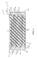
- Fig. 1 illustrates a non-limiting example of a multi-layer capacitor, hereafter referred to as the capacitor 10. While the illustration shows a configuration that is sometimes referred to as a stacked capacitor, it is contemplated that the teachings presented herein are also applicable to other capacitor configurations such as wound capacitors, see Fig. 2 .
- the capacitor 10 includes or defines an anode 12 that includes or is formed of one or more layers 14A of conductive material, and a cathode 16 that includes or is formed of one or more layers 14B of conductive material interlaced (i.e. alternating layers) with the layers 14A of the anode 12.
- Wound capacitors typically have a single conductive layer for the anode, and a single conductive layer for the cathode.
- the layers 14A and 14B may be formed of aluminum or other conductive metals as will be recognized by those in the capacitor arts.
- the layers 14A and 14B may include edge metallization 18A and 18B formed of, for example, a 400 ⁇ thick layer of zinc. It is contemplated that the capacitor 10 can be either polarized or non-polarized. That is, the use of the modifiers 'anode' and 'cathode' are only for the purpose of distinguishing the two electrical connections, and not meant to suggest in any way that the capacitor described herein is necessarily a polarized capacitor.
- the capacitor 10 also includes an arrangement of a dielectric material 20 interposed between each of the layers 14A and 14B of the anode 12 and the cathode 16, respectively.
- the dielectric material 20 may be, for example, a 2.5um thick layer of polypropylene (PP) film.
- PP polypropylene
- the width, length, thickness of dielectric, and number of layers used to form the capacitor 10 may be varied to achieve a desired capacitance value of the capacitor 10, as will be recognized by those in the capacitor arts.
- the capacitor 10 may also include a first endcap 22A configured to electrically and mechanically interconnect each of the layers 14A of the anode 12, and a second endcap 22B configured to mechanically and electrically interconnect each of the layers 14B of the cathode 16.
- the first endcap 22A and the second endcap 22B are formed of conductive nano material.
- Nano material may include various mixtures of Al, Ag, Cu, Zn, or other suitable conductive metals and is available from nanoComposix of San Diego, CA or NovaCentrix of Austin, TX.
- the nano material can be dispersed in a binder material to provide a thick-film ink type material, or in the form of a tape, tube or other disposable material to hold the nano material in place.
- the nano material is briefly exposed to an energy source to cause the nano materials to self-sinter.
- energy sources include a spark, matches (fire), a camera flash, and a beam from a laser.
- the amount of nano material needed is preferably enough (and may require multiple passes of apply nano-material and sintering) to form a low-resistance electrical connection to the edge metallization 18A and 18B, for example a resistance less than 2 ⁇ / ⁇ .
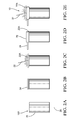
- Figs. 2A-2E illustrates a non-limiting example of a sequence of steps that can be used to electrically attach a first lead 24 to a body portion 26 the capacitor 10.
- Fig. 2A in this example illustrates the capacitor 10 as a wound type capacitor where the body portion 26 includes the layers 14A and 14B, and the dielectric material 20 wound around an axis 28. Accordingly, the edge metallization 18A may be exposed on the end of the body portion 26. It should be recognized that the orientation of the layers 14A and 14B for Figs 2A-2E are oriented perpendicular to that shown in Fig. 1 .
- Fig. 2B illustrates the body portion 26 with nano material 34 applied to the end of the body portion 26.
- the nano material 34 may be a preformed part, or may be in the form of a paste or powder that is applied to the body portion 26 using any of a variety of known techniques.
- Fig. 2C illustrates the first endcap 22A attached to the body portion 26 after energy 30 is applied to the un-sintered nano material 34 to form the first endcap 22A by self-sintering of the nano material 34.
- Fig. 2D illustrates the first lead 24 placed onto the first endcap 22A with an additional layer of un-sintered nano material 34 applied over and/or around the first lead 24.
- the first lead 24 may be a wire or ribbon of electrically conductive material such as zinc coated copper.
- Fig. 2E illustrates how the first lead 24 is electrically attached to the first endcap 22A when the additional un-sintered nano material 34 is sintered following an exposure to energy 32 whereby nano material is used to electrically attach the first lead 24 to the first endcap 22A.
- the steps of forming the first endcap 22A and electrically attaching the first lead 24 may be combined.
- the nano material could be dispersed in a in a manner similar to that described above after placing a wire or other electrical interconnect in contact with the previously applied but un-sintered nano material, and then all of the un-sintered nano material self-sintered at one time as describe above.
- the combined lead attach process mentioned above can be a two-step process where electrical interconnection of the edge metallization nano material is done first, the first lead 24 is electrically attached by a second application of nano materials.
- a capacitor to capacitor interconnect can be formed in a similar way where the electrical interconnect is replaced with another capacitor. This creates either a series or parallel connection of multiple capacitors.
- the capacitor 10 may include a second lead (not shown) electrically attached to the second endcap 22B.
- the second lead may be attached using any of the techniques described above, and may be attached at the same time as the first lead 24 is attached, or as part of a separate process.
- a wire or bus bar (e.g. the first lead 24) may be electrically and mechanically attached to an endcap (e.g. the first endcap 22A or the second endcap 22B) in the same way the endcap was formed.
- the first lead 24 maybe soldered to the first endcap 22A.
- Fig. 3 illustrates a non-limiting example of a method 300 of forming an endcap (e.g. the first endcap 22A or the second endcap 22B) of the capacitor 10 configured to interconnect one or more layers (e.g. the layers 14A and 14B) of conductive material.
- an endcap e.g. the first endcap 22A or the second endcap 22B
- the capacitor 10 configured to interconnect one or more layers (e.g. the layers 14A and 14B) of conductive material.
- Step 310 may include applying conductive nano material (e.g. the nano material 34) to exposed conductive surfaces (e.g. - the edge metallization 18A and 18B) either or both the anode 12 and the cathode 16.
- conductive nano material e.g. the nano material 34
- exposed conductive surfaces e.g. - the edge metallization 18A and 18B
- Step 320 may include exposing the nano material 34 to a source of energy effective to initiate self-sintering of the nano material 34 such as a spark, matches (fire), a camera flash, or a beam from a laser.
- a source of energy effective to initiate self-sintering of the nano material 34 such as a spark, matches (fire), a camera flash, or a beam from a laser.
- Step 330 PLACE LEAD IN CONTACT NANO MATERIAL, may include placing a lead (e.g. the first lead 24) in contact with the nano material 34. Step 330 may be followed by the application of additional nano material and another self-sintering process to electrically attach the lead to the previously formed endcap. It is contemplated that steps 320 and 330 could be reversed relative to the order shown in Fig. 3 so the lead could be attached by one or more applications of un-sintered nano material followed by a single sintering step. Alternatively, the lead could be attached to a sintered endcap by other methods such as soldering.
- a way to form electrical connections between conductor layers of a capacitor is provided.
- This process could also be used to interconnect capacitor to capacitor in either a series or parallel connection.
- This process is generally faster and yields a higher quality electrical connection as the connection is a solid layer of dense metal as opposed to an interconnection of molten metal dots provided by Babbitt metal.
- the process described herein has no overspray which eliminates the masking, unmasking and cleaning steps found in the arc spray process.
- the process can readily form electrical connections with different thickness layers without intrusion of metals to the inner layers of the capacitor, and lowers the overall temperatures necessary to form electrical connections when compared to the arc spray process.
- an end cap may require one or more layers of nano metals where each one sintered by an energy source to achieve the desired electrical resistance. Multiple layers may be advantageous as self-sintering one thick layer of nano metal may generate enough heat to melt materials underlying the nano metal. As such, it may be advantageous to build up a thick layer by a progression of lower energy sintering steps.
Landscapes
- Engineering & Computer Science (AREA)
- Power Engineering (AREA)
- Manufacturing & Machinery (AREA)
- Microelectronics & Electronic Packaging (AREA)
- Fixed Capacitors And Capacitor Manufacturing Machines (AREA)
Abstract
Description
- This disclosure generally relates to a multi-layer capacitor, and more particularly relates to a capacitor with endcaps formed of conductive nano material.
- Metallized film capacitors typically form electrical and mechanical connections between layers of conductors separated by dielectric films using an arc spray process. Arc spray uses DC power to energize two conductive wires of Babbitt metal by applying a voltage to one wire relative to the other. This energized wire is then fed through a feeder into a gun head. It is at the gun head that the wires meet and arc against each other, thereby creating molten material. Then dry compressed air is introduced to the arc zone, the molten material is atomized into tiny droplets that are propelled toward a prepared part or target. As the droplets hit the target, they flatten out and make molten dots. The molten dots interlock one on top another and form a mechanical and electrical bond.
- This arc spray process is generally considered to be a messy, time consuming process, involving preparing the target surface, cleaning, wrapping other surfaces to protect other surfaces from over spray, spraying, removing wrapping, cleaning of the overspray surfaces and inspection depending on the application lead attachment, welding or soldering is then performed. The electrical interconnection formed by the arc spray process is sometimes considered to be a weak link in a capacitor's design. Furthermore, the arc spray process can cause intrusion of the Babbitt material into the inner layers of the capacitor, which can lead to shorts and reduced capacitance.
- In accordance with one embodiment, a multi-layer capacitor is provided. The capacitor includes an anode, a cathode, a dielectric material, a first endcap, and a second endcap. The anode is formed of one or more layers of conductive material. The cathode is formed of one or more layers of conductive material interlaced with the layers of the anode. The dielectric material is interposed between each of the layers of the anode and the cathode e. The first endcap is configured to interconnect each of the layers of the anode. The second endcap is configured to interconnect each of the layers of the cathode. The first endcap and the second endcap are formed of conductive nano material.
- The capacitor may further comprise a first lead electrically attached to the first endcap, wherein conductive nano material is used to electrically attach the first lead to the first end cap. The first lead may be electrically attached to the first endcap when the first end cap is formed. The capacitor may further comprise a second lead electrically attached to the second endcap, wherein conductive nano material is used to electrically attach the second lead to the second end cap. The second lead may be electrically attached to the second endcap when the second end cap is formed.
- In another embodiment, a method of forming an endcap of a capacitor configured to interconnect one or more layers of conductive material is provided. The method includes the step of applying conductive nano material to exposed conductive surfaces of at least one of an anode and a cathode of the one or more layers of conductive material. The method also includes the step of exposing the nano material to a source of energy effective to initiate self-sintering of the nano material.
- The method may include a step of placing a lead in contact with the conductive nano material.
- Further features and advantages will appear more clearly on a reading of the following detailed description of the preferred embodiment, which is given by way of non-limiting example only and with reference to the accompanying drawings.
- The present invention will now be described, by way of example with reference to the accompanying drawings, in which:
-
Fig. 1 is a sectional side view of a capacitor with endcaps formed of nano material in accordance with one embodiment; -
Figs. 2A-2E are a sequence of illustrations showing fabrication steps of the capacitor ofFig. 1 in accordance with one embodiment; and -
Fig. 3 is flowchart of a method of forming an endcap of the capacitor ofFig. 1 in accordance with one embodiment. - Described herein is a means to form electrical connections between conductive layers or plates of a capacitor using nano metal materials or nano materials that are self-sintered after exposure to a source of energy effective to initiate sintering of the nano material. Optionally, nano materials may also be used to attach an electrically conductive lead or wire to the capacitor.
-
Fig. 1 illustrates a non-limiting example of a multi-layer capacitor, hereafter referred to as thecapacitor 10. While the illustration shows a configuration that is sometimes referred to as a stacked capacitor, it is contemplated that the teachings presented herein are also applicable to other capacitor configurations such as wound capacitors, seeFig. 2 . In general, thecapacitor 10 includes or defines ananode 12 that includes or is formed of one ormore layers 14A of conductive material, and acathode 16 that includes or is formed of one ormore layers 14B of conductive material interlaced (i.e. alternating layers) with thelayers 14A of theanode 12. Wound capacitors typically have a single conductive layer for the anode, and a single conductive layer for the cathode. Thelayers layers edge metallization capacitor 10 can be either polarized or non-polarized. That is, the use of the modifiers 'anode' and 'cathode' are only for the purpose of distinguishing the two electrical connections, and not meant to suggest in any way that the capacitor described herein is necessarily a polarized capacitor. - The
capacitor 10 also includes an arrangement of adielectric material 20 interposed between each of thelayers anode 12 and thecathode 16, respectively. Thedielectric material 20 may be, for example, a 2.5um thick layer of polypropylene (PP) film. The width, length, thickness of dielectric, and number of layers used to form thecapacitor 10 may be varied to achieve a desired capacitance value of thecapacitor 10, as will be recognized by those in the capacitor arts. - The
capacitor 10 may also include afirst endcap 22A configured to electrically and mechanically interconnect each of thelayers 14A of theanode 12, and asecond endcap 22B configured to mechanically and electrically interconnect each of thelayers 14B of thecathode 16. Preferably, thefirst endcap 22A and thesecond endcap 22B are formed of conductive nano material. Nano material may include various mixtures of Al, Ag, Cu, Zn, or other suitable conductive metals and is available from nanoComposix of San Diego, CA or NovaCentrix of Austin, TX. The nano material can be dispersed in a binder material to provide a thick-film ink type material, or in the form of a tape, tube or other disposable material to hold the nano material in place. Once dispersed, the nano material is briefly exposed to an energy source to cause the nano materials to self-sinter. Some non-limiting examples of energy sources include a spark, matches (fire), a camera flash, and a beam from a laser. The amount of nano material needed is preferably enough (and may require multiple passes of apply nano-material and sintering) to form a low-resistance electrical connection to theedge metallization -
Figs. 2A-2E illustrates a non-limiting example of a sequence of steps that can be used to electrically attach afirst lead 24 to abody portion 26 thecapacitor 10.Fig. 2A in this example illustrates thecapacitor 10 as a wound type capacitor where thebody portion 26 includes thelayers dielectric material 20 wound around anaxis 28. Accordingly, theedge metallization 18A may be exposed on the end of thebody portion 26. It should be recognized that the orientation of thelayers Figs 2A-2E are oriented perpendicular to that shown inFig. 1 . -
Fig. 2B illustrates thebody portion 26 withnano material 34 applied to the end of thebody portion 26. As suggested above, thenano material 34 may be a preformed part, or may be in the form of a paste or powder that is applied to thebody portion 26 using any of a variety of known techniques. -
Fig. 2C illustrates thefirst endcap 22A attached to thebody portion 26 afterenergy 30 is applied to theun-sintered nano material 34 to form thefirst endcap 22A by self-sintering of thenano material 34. -
Fig. 2D illustrates thefirst lead 24 placed onto thefirst endcap 22A with an additional layer ofun-sintered nano material 34 applied over and/or around thefirst lead 24. Thefirst lead 24 may be a wire or ribbon of electrically conductive material such as zinc coated copper. -
Fig. 2E illustrates how thefirst lead 24 is electrically attached to thefirst endcap 22A when the additionalun-sintered nano material 34 is sintered following an exposure toenergy 32 whereby nano material is used to electrically attach thefirst lead 24 to thefirst endcap 22A. - Alternatively, the steps of forming the
first endcap 22A and electrically attaching thefirst lead 24 may be combined. For example, the nano material could be dispersed in a in a manner similar to that described above after placing a wire or other electrical interconnect in contact with the previously applied but un-sintered nano material, and then all of the un-sintered nano material self-sintered at one time as describe above. Or as previously described, the combined lead attach process mentioned above can be a two-step process where electrical interconnection of the edge metallization nano material is done first, thefirst lead 24 is electrically attached by a second application of nano materials. A capacitor to capacitor interconnect can be formed in a similar way where the electrical interconnect is replaced with another capacitor. This creates either a series or parallel connection of multiple capacitors. - Similarly, the
capacitor 10 may include a second lead (not shown) electrically attached to thesecond endcap 22B. The second lead may be attached using any of the techniques described above, and may be attached at the same time as thefirst lead 24 is attached, or as part of a separate process. - As described above, a wire or bus bar (e.g. the first lead 24) may be electrically and mechanically attached to an endcap (e.g. the
first endcap 22A or thesecond endcap 22B) in the same way the endcap was formed. Alternatively, thefirst lead 24 maybe soldered to thefirst endcap 22A. -
Fig. 3 illustrates a non-limiting example of amethod 300 of forming an endcap (e.g. thefirst endcap 22A or thesecond endcap 22B) of thecapacitor 10 configured to interconnect one or more layers (e.g. thelayers -
Step 310, APPLY NANO MATERIAL, may include applying conductive nano material (e.g. the nano material 34) to exposed conductive surfaces (e.g. - theedge metallization anode 12 and thecathode 16. -
Step 320, SINTER NANO MATERIAL, may include exposing thenano material 34 to a source of energy effective to initiate self-sintering of thenano material 34 such as a spark, matches (fire), a camera flash, or a beam from a laser. -
Step 330, PLACE LEAD IN CONTACT NANO MATERIAL, may include placing a lead (e.g. the first lead 24) in contact with thenano material 34. Step 330 may be followed by the application of additional nano material and another self-sintering process to electrically attach the lead to the previously formed endcap. It is contemplated thatsteps Fig. 3 so the lead could be attached by one or more applications of un-sintered nano material followed by a single sintering step. Alternatively, the lead could be attached to a sintered endcap by other methods such as soldering. - Accordingly, a way to form electrical connections between conductor layers of a capacitor is provided. This process could also be used to interconnect capacitor to capacitor in either a series or parallel connection. This process is generally faster and yields a higher quality electrical connection as the connection is a solid layer of dense metal as opposed to an interconnection of molten metal dots provided by Babbitt metal. Unlike the known arc spray process, the process described herein has no overspray which eliminates the masking, unmasking and cleaning steps found in the arc spray process. The process can readily form electrical connections with different thickness layers without intrusion of metals to the inner layers of the capacitor, and lowers the overall temperatures necessary to form electrical connections when compared to the arc spray process. It is recognized that an end cap may require one or more layers of nano metals where each one sintered by an energy source to achieve the desired electrical resistance. Multiple layers may be advantageous as self-sintering one thick layer of nano metal may generate enough heat to melt materials underlying the nano metal. As such, it may be advantageous to build up a thick layer by a progression of lower energy sintering steps.
- While this invention has been described in terms of the preferred embodiments thereof, it is not intended to be so limited, but rather only to the extent set forth in the claims that follow.
Claims (7)
- A multi-layer capacitor (10) comprising:an anode (12) formed of one or more layers (14A) of conductive material;a cathode (16) formed of one or more layers (14B) of conductive material interlaced with the layers (14A) of the anode (12);a dielectric material (20) interposed between each of the layers (14A, 14B) of the anode (12) and the cathode (16);
a first endcap (22A) configured to interconnect each of the layers (14A) of the anode (12); anda second endcap (22B) configured to interconnect each of the layers (14B) of the cathode (16), whereinthe first endcap (22A) and the second endcap (22B) are formed of conductive nano material (34). - Capacitor (10) in accordance with claim 1, wherein capacitor (10) further comprises
a first lead (24) electrically attached to the first endcap (22A), wherein conductive nano material (34) is used to electrically attach the first lead (24) to the first end cap. - The capacitor (10) in accordance with claim 2, wherein the first lead (24) is electrically attached to the first endcap (22A) when the first end cap is formed.
- Capacitor (10) according to any one of the preceding claims, wherein capacitor (10) further comprises
a second lead electrically attached to the second endcap (22B), wherein conductive nano material (34) is used to electrically attach the second lead to the second end cap. - Capacitor (10) in accordance with claim 4, wherein the second lead is electrically attached to the second endcap (22B) when the second end cap is formed.
- A method (300) of forming an endcap of a capacitor (10) configured to interconnect one or more layers (14A, 14B) of conductive material, said method (300) comprising:applying conductive nano material (34) to exposed conductive surfaces of at least one of an anode (12) and a cathode (16) of the one or more layers (14A, 14B) of conductive material; andexposing the nano material (34) to a source of energy (30) effective to initiate self-sintering of the nano material (34).
- Method (300) in accordance with claim 6, wherein the method (300) includes
placing a lead in contact with the conductive nano material (34).
Applications Claiming Priority (2)
| Application Number | Priority Date | Filing Date | Title |
|---|---|---|---|
| US201361874409P | 2013-09-06 | 2013-09-06 | |
| US14/320,979 US20150070816A1 (en) | 2013-09-06 | 2014-07-01 | Capacitor fabrication using nano materials |
Publications (1)
| Publication Number | Publication Date |
|---|---|
| EP2846338A1 true EP2846338A1 (en) | 2015-03-11 |
Family
ID=51352462
Family Applications (1)
| Application Number | Title | Priority Date | Filing Date |
|---|---|---|---|
| EP14181285.9A Withdrawn EP2846338A1 (en) | 2013-09-06 | 2014-08-18 | Capacitor fabrication using nano materials |
Country Status (3)
| Country | Link |
|---|---|
| US (1) | US20150070816A1 (en) |
| EP (1) | EP2846338A1 (en) |
| CN (1) | CN104425129A (en) |
Families Citing this family (1)
| Publication number | Priority date | Publication date | Assignee | Title |
|---|---|---|---|---|
| CN108025178B (en) * | 2015-09-16 | 2021-09-28 | 心脏起搏器股份公司 | Assembly technique for sintered anodes and sintered cathodes |
Citations (3)
| Publication number | Priority date | Publication date | Assignee | Title |
|---|---|---|---|---|
| EP1965397A1 (en) * | 2005-12-22 | 2008-09-03 | Namics Corporation | Thermosetting conductive paste and multilayer ceramic component having external electrode which is formed by using such thermosetting conductive paste |
| US20110141657A1 (en) * | 2009-12-14 | 2011-06-16 | Samsung Electro-Mechanics Co., Ltd. | Conductive paste compound for external electrode, multilayer ceramic capacitor including the same, and manufacturing method thereof |
| US20130120899A1 (en) * | 2011-11-14 | 2013-05-16 | Samsung Electro-Mechanics Co., Ltd. | Multilayer ceramic electronic part and method of manufacturing the same |
Family Cites Families (7)
| Publication number | Priority date | Publication date | Assignee | Title |
|---|---|---|---|---|
| US3967168A (en) * | 1975-06-26 | 1976-06-29 | Illinois Tool Works Inc. | Electrical capacitor having alternating metallized nonheat-shrinkable dielectric layers and heat-shrinkable dielectric layers |
| US4102021A (en) * | 1975-10-06 | 1978-07-25 | Matsushita Electric Industrial Co., Ltd. | Method for making capacitors with plated terminals |
| US4356529A (en) * | 1981-01-21 | 1982-10-26 | Sprague Electric Company | Terminated monolithic ceramic chip capacitor |
| US4477953A (en) * | 1981-07-06 | 1984-10-23 | Lobo Edward M | Wound capacitor end connections and method of obtaining same |
| FR2663149B1 (en) * | 1990-06-08 | 1993-09-17 | Europ Composants Electron | SHEET CAPACITOR AND METHOD FOR MANUFACTURING SUCH A CAPACITOR. |
| JP3330836B2 (en) * | 1997-01-22 | 2002-09-30 | 太陽誘電株式会社 | Manufacturing method of laminated electronic components |
| FI122009B (en) * | 2007-06-08 | 2011-07-15 | Teknologian Tutkimuskeskus Vtt | Structures based on nanoparticles and process for their preparation |
-
2014
- 2014-07-01 US US14/320,979 patent/US20150070816A1/en not_active Abandoned
- 2014-08-18 EP EP14181285.9A patent/EP2846338A1/en not_active Withdrawn
- 2014-09-01 CN CN201410440049.9A patent/CN104425129A/en active Pending
Patent Citations (3)
| Publication number | Priority date | Publication date | Assignee | Title |
|---|---|---|---|---|
| EP1965397A1 (en) * | 2005-12-22 | 2008-09-03 | Namics Corporation | Thermosetting conductive paste and multilayer ceramic component having external electrode which is formed by using such thermosetting conductive paste |
| US20110141657A1 (en) * | 2009-12-14 | 2011-06-16 | Samsung Electro-Mechanics Co., Ltd. | Conductive paste compound for external electrode, multilayer ceramic capacitor including the same, and manufacturing method thereof |
| US20130120899A1 (en) * | 2011-11-14 | 2013-05-16 | Samsung Electro-Mechanics Co., Ltd. | Multilayer ceramic electronic part and method of manufacturing the same |
Also Published As
| Publication number | Publication date |
|---|---|
| US20150070816A1 (en) | 2015-03-12 |
| CN104425129A (en) | 2015-03-18 |
Similar Documents
| Publication | Publication Date | Title |
|---|---|---|
| US12224104B2 (en) | Electronic component | |
| US11919084B2 (en) | Electronic component and method for manufacturing the same | |
| KR101645625B1 (en) | Electronic component and method for forming junction structure between electronic component and object to be joined | |
| US3581159A (en) | Solid electrolyte capacitor having improved counterelectrode system | |
| CN102290552B (en) | Hoop-shaped part for aluminum tab | |
| US10381152B2 (en) | Coil component and coil-component-equipped mounting substrate | |
| JP6481776B2 (en) | Coil component and manufacturing method thereof | |
| US11551872B2 (en) | Multilayer ceramic capacitor | |
| US10944228B2 (en) | Method for attaching a contact element to the end of an electrical conductor | |
| EP2844414B1 (en) | Method of producing a metallised substrate consisting of aluminium | |
| US20150070816A1 (en) | Capacitor fabrication using nano materials | |
| JP2016171041A (en) | Method of manufacturing aluminum wire with terminal | |
| WO2019037928A1 (en) | SOLAR CELL CONNECTOR WITH FUNCTIONAL LENGTH COATING | |
| US20170325290A1 (en) | Method for Producing a Contact Region for a Layer of an Electrical Heating Device and Apparatus for an Electrical Heating Device for a Motor Vehicle | |
| JP4333594B2 (en) | Conductive paste and ceramic electronic components | |
| DE2645129A1 (en) | Film capacitor and process for its manufacture | |
| JP2012119373A (en) | Manufacturing method of laminated coil component | |
| JP2018016845A (en) | Alloy for thermal spraying, alloy wire for thermal spraying, film capacitor, and solder alloy | |
| JP5915798B2 (en) | Multilayer ceramic electronic components | |
| JP2023029164A (en) | Conductive paste, and lamination type ceramic component using the same | |
| TW200931457A (en) | Terminal electrode of passive component | |
| JPH027410A (en) | Chip-shaped electronic component and its manufacture |
Legal Events
| Date | Code | Title | Description |
|---|---|---|---|
| 17P | Request for examination filed |
Effective date: 20140818 |
|
| AK | Designated contracting states |
Kind code of ref document: A1 Designated state(s): AL AT BE BG CH CY CZ DE DK EE ES FI FR GB GR HR HU IE IS IT LI LT LU LV MC MK MT NL NO PL PT RO RS SE SI SK SM TR |
|
| AX | Request for extension of the european patent |
Extension state: BA ME |
|
| PUAI | Public reference made under article 153(3) epc to a published international application that has entered the european phase |
Free format text: ORIGINAL CODE: 0009012 |
|
| R17P | Request for examination filed (corrected) |
Effective date: 20150911 |
|
| RBV | Designated contracting states (corrected) |
Designated state(s): AL AT BE BG CH CY CZ DE DK EE ES FI FR GB GR HR HU IE IS IT LI LT LU LV MC MK MT NL NO PL PT RO RS SE SI SK SM TR |
|
| 17Q | First examination report despatched |
Effective date: 20190211 |
|
| STAA | Information on the status of an ep patent application or granted ep patent |
Free format text: STATUS: THE APPLICATION IS DEEMED TO BE WITHDRAWN |
|
| 18D | Application deemed to be withdrawn |
Effective date: 20190622 |