EP2846085A1 - A lighting device and corresponding method - Google Patents
A lighting device and corresponding method Download PDFInfo
- Publication number
- EP2846085A1 EP2846085A1 EP14183688.2A EP14183688A EP2846085A1 EP 2846085 A1 EP2846085 A1 EP 2846085A1 EP 14183688 A EP14183688 A EP 14183688A EP 2846085 A1 EP2846085 A1 EP 2846085A1
- Authority
- EP
- European Patent Office
- Prior art keywords
- light radiation
- mounting board
- radiation source
- holder
- face
- Prior art date
- Legal status (The legal status is an assumption and is not a legal conclusion. Google has not performed a legal analysis and makes no representation as to the accuracy of the status listed.)
- Granted
Links
Images

Classifications
-
- F—MECHANICAL ENGINEERING; LIGHTING; HEATING; WEAPONS; BLASTING
- F21—LIGHTING
- F21V—FUNCTIONAL FEATURES OR DETAILS OF LIGHTING DEVICES OR SYSTEMS THEREOF; STRUCTURAL COMBINATIONS OF LIGHTING DEVICES WITH OTHER ARTICLES, NOT OTHERWISE PROVIDED FOR
- F21V31/00—Gas-tight or water-tight arrangements
- F21V31/005—Sealing arrangements therefor
-
- F—MECHANICAL ENGINEERING; LIGHTING; HEATING; WEAPONS; BLASTING
- F21—LIGHTING
- F21K—NON-ELECTRIC LIGHT SOURCES USING LUMINESCENCE; LIGHT SOURCES USING ELECTROCHEMILUMINESCENCE; LIGHT SOURCES USING CHARGES OF COMBUSTIBLE MATERIAL; LIGHT SOURCES USING SEMICONDUCTOR DEVICES AS LIGHT-GENERATING ELEMENTS; LIGHT SOURCES NOT OTHERWISE PROVIDED FOR
- F21K9/00—Light sources using semiconductor devices as light-generating elements, e.g. using light-emitting diodes [LED] or lasers
- F21K9/90—Methods of manufacture
-
- H—ELECTRICITY
- H10—SEMICONDUCTOR DEVICES; ELECTRIC SOLID-STATE DEVICES NOT OTHERWISE PROVIDED FOR
- H10H—INORGANIC LIGHT-EMITTING SEMICONDUCTOR DEVICES HAVING POTENTIAL BARRIERS
- H10H20/00—Individual inorganic light-emitting semiconductor devices having potential barriers, e.g. light-emitting diodes [LED]
- H10H20/80—Constructional details
- H10H20/85—Packages
- H10H20/857—Interconnections, e.g. lead-frames, bond wires or solder balls
-
- F—MECHANICAL ENGINEERING; LIGHTING; HEATING; WEAPONS; BLASTING
- F21—LIGHTING
- F21V—FUNCTIONAL FEATURES OR DETAILS OF LIGHTING DEVICES OR SYSTEMS THEREOF; STRUCTURAL COMBINATIONS OF LIGHTING DEVICES WITH OTHER ARTICLES, NOT OTHERWISE PROVIDED FOR
- F21V19/00—Fastening of light sources or lamp holders
- F21V19/001—Fastening of light sources or lamp holders the light sources being semiconductors devices, e.g. LEDs
- F21V19/003—Fastening of light source holders, e.g. of circuit boards or substrates holding light sources
- F21V19/005—Fastening of light source holders, e.g. of circuit boards or substrates holding light sources by permanent fixing means, e.g. gluing, riveting or embedding in a potting compound
-
- F—MECHANICAL ENGINEERING; LIGHTING; HEATING; WEAPONS; BLASTING
- F21—LIGHTING
- F21V—FUNCTIONAL FEATURES OR DETAILS OF LIGHTING DEVICES OR SYSTEMS THEREOF; STRUCTURAL COMBINATIONS OF LIGHTING DEVICES WITH OTHER ARTICLES, NOT OTHERWISE PROVIDED FOR
- F21V23/00—Arrangement of electric circuit elements in or on lighting devices
- F21V23/003—Arrangement of electric circuit elements in or on lighting devices the elements being electronics drivers or controllers for operating the light source, e.g. for a LED array
- F21V23/004—Arrangement of electric circuit elements in or on lighting devices the elements being electronics drivers or controllers for operating the light source, e.g. for a LED array arranged on a substrate, e.g. a printed circuit board
- F21V23/005—Arrangement of electric circuit elements in or on lighting devices the elements being electronics drivers or controllers for operating the light source, e.g. for a LED array arranged on a substrate, e.g. a printed circuit board the substrate is supporting also the light source
-
- H—ELECTRICITY
- H10—SEMICONDUCTOR DEVICES; ELECTRIC SOLID-STATE DEVICES NOT OTHERWISE PROVIDED FOR
- H10H—INORGANIC LIGHT-EMITTING SEMICONDUCTOR DEVICES HAVING POTENTIAL BARRIERS
- H10H20/00—Individual inorganic light-emitting semiconductor devices having potential barriers, e.g. light-emitting diodes [LED]
- H10H20/01—Manufacture or treatment
-
- H—ELECTRICITY
- H10—SEMICONDUCTOR DEVICES; ELECTRIC SOLID-STATE DEVICES NOT OTHERWISE PROVIDED FOR
- H10H—INORGANIC LIGHT-EMITTING SEMICONDUCTOR DEVICES HAVING POTENTIAL BARRIERS
- H10H20/00—Individual inorganic light-emitting semiconductor devices having potential barriers, e.g. light-emitting diodes [LED]
- H10H20/80—Constructional details
- H10H20/85—Packages
- H10H20/8506—Containers
-
- H—ELECTRICITY
- H10—SEMICONDUCTOR DEVICES; ELECTRIC SOLID-STATE DEVICES NOT OTHERWISE PROVIDED FOR
- H10H—INORGANIC LIGHT-EMITTING SEMICONDUCTOR DEVICES HAVING POTENTIAL BARRIERS
- H10H20/00—Individual inorganic light-emitting semiconductor devices having potential barriers, e.g. light-emitting diodes [LED]
- H10H20/80—Constructional details
- H10H20/85—Packages
- H10H20/852—Encapsulations
- H10H20/854—Encapsulations characterised by their material, e.g. epoxy or silicone resins
-
- F—MECHANICAL ENGINEERING; LIGHTING; HEATING; WEAPONS; BLASTING
- F21—LIGHTING
- F21Y—INDEXING SCHEME ASSOCIATED WITH SUBCLASSES F21K, F21L, F21S and F21V, RELATING TO THE FORM OR THE KIND OF THE LIGHT SOURCES OR OF THE COLOUR OF THE LIGHT EMITTED
- F21Y2101/00—Point-like light sources
-
- F—MECHANICAL ENGINEERING; LIGHTING; HEATING; WEAPONS; BLASTING
- F21—LIGHTING
- F21Y—INDEXING SCHEME ASSOCIATED WITH SUBCLASSES F21K, F21L, F21S and F21V, RELATING TO THE FORM OR THE KIND OF THE LIGHT SOURCES OR OF THE COLOUR OF THE LIGHT EMITTED
- F21Y2115/00—Light-generating elements of semiconductor light sources
- F21Y2115/10—Light-emitting diodes [LED]
-
- H—ELECTRICITY
- H10—SEMICONDUCTOR DEVICES; ELECTRIC SOLID-STATE DEVICES NOT OTHERWISE PROVIDED FOR
- H10H—INORGANIC LIGHT-EMITTING SEMICONDUCTOR DEVICES HAVING POTENTIAL BARRIERS
- H10H20/00—Individual inorganic light-emitting semiconductor devices having potential barriers, e.g. light-emitting diodes [LED]
- H10H20/01—Manufacture or treatment
- H10H20/036—Manufacture or treatment of packages
-
- H—ELECTRICITY
- H10—SEMICONDUCTOR DEVICES; ELECTRIC SOLID-STATE DEVICES NOT OTHERWISE PROVIDED FOR
- H10H—INORGANIC LIGHT-EMITTING SEMICONDUCTOR DEVICES HAVING POTENTIAL BARRIERS
- H10H20/00—Individual inorganic light-emitting semiconductor devices having potential barriers, e.g. light-emitting diodes [LED]
- H10H20/01—Manufacture or treatment
- H10H20/036—Manufacture or treatment of packages
- H10H20/0362—Manufacture or treatment of packages of encapsulations
-
- H—ELECTRICITY
- H10—SEMICONDUCTOR DEVICES; ELECTRIC SOLID-STATE DEVICES NOT OTHERWISE PROVIDED FOR
- H10W—GENERIC PACKAGES, INTERCONNECTIONS, CONNECTORS OR OTHER CONSTRUCTIONAL DETAILS OF DEVICES COVERED BY CLASS H10
- H10W90/00—Package configurations
- H10W90/701—Package configurations characterised by the relative positions of pads or connectors relative to package parts
- H10W90/721—Package configurations characterised by the relative positions of pads or connectors relative to package parts of bump connectors
- H10W90/724—Package configurations characterised by the relative positions of pads or connectors relative to package parts of bump connectors between a chip and a stacked insulating package substrate, interposer or RDL
Definitions
- the present description relates to lighting devices.
- One or more embodiments may refer to Solid State Lighting (SSL) devices, such as lighting devices which make use of LED sources.
- SSL Solid State Lighting
- solid state lighting modules for example flexible LED modules
- the electrical and electronic components (light radiation source(s), resistors, capacitors, LED drivers etc.) are mounted on a single side of a board (e.g. similar to a Printed Circuit Board, PCB).
- a board e.g. similar to a Printed Circuit Board, PCB.
- all components therefore are located on the side which is visible to the end user, with possible disadvantages of various kinds.
- the choice of the electrical and electronic components if the number of such components is high, the radiation pattern may be uneven, with a consequent reduction of the device efficiency.
- the electrical/electronic components are usually black or dark, and this colour may eventually produce visible black spots when the lighting module is off.
- the drawback might also be limited by covering the dark components with a coating, for example a silicone coating, of a white colour, without covering the light radiation sources, also taking into account the fact that the sealing from the outer environment (IP protection) may be achieved with a two-step process:
- the light radiation sources which must remain exposed
- the drive circuitry which on the contrary must be covered and masked by a white layer
- such a process may impose limitations in the choice of sources, e.g. because of the difficulty of using LEDs with high performance and reliability and low cost.
- Another constraint may come from the fact that the LED-to-LED pitch is influenced by the space needed to mount the other electrical and electronic components.
- One or more embodiments aim at overcoming the previously outlined drawbacks.
- such an object may be achieved thanks to a device having the features set forth in the claims that follow.
- One or more embodiments may refer to a corresponding method.
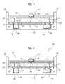
- FIG. 1 to 4 shows subsequent steps of a method for obtaining, according to one or more embodiments, a lighting device 10 which makes use, as a light radiation source 12, of a solid state source, such as a LED source (either single or plural: for simplicity, the figures refer to a single source 12).
- a lighting device 10 which makes use, as a light radiation source 12, of a solid state source, such as a LED source (either single or plural: for simplicity, the figures refer to a single source 12).
- the source 12 may be mounted on a board 14, substantially similar to a printed circuit board.
- the board 14 may be made of an electrically insulating material, e.g. (optionally flexible) polyimide.
- the board 14 may have two opposite faces, on which there are formed, according to known criteria, conductive lines 16 (of an electrically conductive material, e.g. copper) that are adapted to define transmission paths for electrical (supply and/or control) signals which connect the source 12 to drive circuits, which are denoted on the whole by 18.
- conductive lines 16 of an electrically conductive material, e.g. copper
- electrical (supply and/or control) signals which connect the source 12 to drive circuits, which are denoted on the whole by 18.
- the source 12 and the components 18 may be connected (optionally also mechanically) to the lines 16 by soldering and/or via an electrically conductive adhesive, as schematically shown at 20 in Figure 2 and the following Figures.
- lines or connection "vias" 24 for the electrical connection between the source 12, mounted on the "front” face of the board 14, and the drive circuits 18, which on the contrary are mounted on the "back” face of board 14.
- the front face of the board 14 only the light radiation source(s) 12 is/are visible from the outside, while the drive circuits 18, mounted on the opposite face, i.e. on the back face, are hidden from the outside.
- a lighting module or device 10 is implemented that has an IP protection grade, and which may be flexible or "flex", thanks to the flexibility of the board 14.
- the components 18 may be mounted on the back face of the board 20, for example via standard methods such as SMD processes and/or by using electrically conductive adhesives or soldering masses, possibly in combination (for example soldered / welded layers and conductive adhesive layers coated in sequence).
- a generally vat-like holder 28 e.g. comprising silicone-based, and therefore flexible material of a generally white colour.
- a holder may be produced e.g. by extrusion or molding.
- the holder 28 can be provided, e.g. in the bottom wall, with cavities 30 adapted to accommodate the circuits 18 mounted on the back face of board 26.
- this enables to match the shape of the holder 28 and the shape of the "bare" module (i.e. the board 14 with the source(s) 12 and components 18 mounted on the opposite faces thereof).
- this bare module may be inserted into the holder 28, as schematically shown in Figure 3 , and then the bare module may be glued to holder 28.
- the holder 28 may have a general vat shape with a bottom wall (where the cavities 30 may be arranged) and peripheral walls 32 adapted to surround the basic module (board 14, light radiation source(s) 12 and components 18) in conditions wherein the side edges 22 of the board 14 contact the side walls 32 of the holder 28, or at least are adjacent to them.
- the figure exemplifies one or more embodiments wherein it is possible to achieve a sealing of the circuit 10, providing it with a protection grade (for example IP) against the penetration of external agents, without having to perform two subsequent steps of applying, first of all, a white sealing mass (e.g. silicone-based), and then a transparent (i.e. light-permeable) mass, according to the criteria recalled in the introduction of the present application.
- a protection grade for example IP
- Figure 4 there is shown the possibility, in one or more embodiments, of achieving a sealing from the environment by applying a single transparent (i.e. light-permeable) sealing mass 34, thereby implementing one single step and reducing the related costs.
- the sealing mass or layer 34 may cover the whole front face of board 13 (including the light radiation source(s); being transparent, the layer 34 does not block light radiation), while sealingly connecting to the side walls 32 of the holder 28, i.e. while sealing the peripheral area where side edges 22 of the board 14 face (e.g. contact) the side walls 32 of the holder 28.
- the sealing mass 34 may therefore extend beyond the contours of the soldering mask, i.e. to areas external to the paths of the lines 16.
- one or more embodiments may make use of two sealing masses or layers:
- Figure 5 shows the possibility to apply a first thin sealing mass or layer 36 of a white colour, which is adapted to cover the front face of the board 26 while leaving the light radiation source(s) 12 exposed.
- the front face of the board 14 there may be only provided the light radiation source(s) 12 (the drive circuits 18 being mounted on the back face); this simplifies the application of a layer 36 of reduced thickness, which leaves the source(s) 12 exposed while extending to cover the front face of the board 14 (and the conductive lines 16 provided thereon) with a substantially planar extension profile, which does not have to "wrap" any circuit component in order to mask it.
- the possible use of a very thin layer 36 opens up a wide range of choice of the light radiation source(s) 12, enabling therefore the use of low-cost LEDs without taking into account factors such as the package size.
- Figure 6 exemplifies that, in one or more embodiments, on the layer 36 it is then possible to apply a subsequent transparent sealing layer 38, of a light-permeable material, which therefore, in the same way as the layer 34 described with reference to Figure 4 , may extend to cover the source(s) 12 as well without blocking the light emission by the device 10.
- the layer 36 and/or the layer 38 may connect sealingly with the side walls 32 of the holder 28, while sealing the peripheral area where the side edges 22 of the board 14 face (e.g. contact) the side walls 32 of the holder 28.
- sealing layers/masses 34, 36, 38 correspond to solutions known per se, so that they do not require a detailed description herein.
Landscapes
- Engineering & Computer Science (AREA)
- General Engineering & Computer Science (AREA)
- Microelectronics & Electronic Packaging (AREA)
- Manufacturing & Machinery (AREA)
- Physics & Mathematics (AREA)
- Optics & Photonics (AREA)
- Fastening Of Light Sources Or Lamp Holders (AREA)
- Led Device Packages (AREA)
- Arrangement Of Elements, Cooling, Sealing, Or The Like Of Lighting Devices (AREA)
- Non-Portable Lighting Devices Or Systems Thereof (AREA)
Abstract
- a mounting board (14) with first and second opposed faces and vias (24) extending therethrough,
- one or more light radiation sources (12), e.g. LED radiation sources, mounted on the first face of the mounting board (14),
- drive circuitry (18) for the light radiation source (12) mounted on the second face of the mounting board (14), with electrically conductive lines (16) between the light radiation source (12) and the drive circuitry (18) passing through said vias (24),
- a vat-like holder (28) housing the mounting board (14) with the light radiation source (12) and the drive circuitry (18) mounted thereon.
Description
- The present description relates to lighting devices.
- One or more embodiments may refer to Solid State Lighting (SSL) devices, such as lighting devices which make use of LED sources.
- Various implementations of solid state lighting modules are known (for example flexible LED modules) in which the electrical and electronic components (light radiation source(s), resistors, capacitors, LED drivers etc.) are mounted on a single side of a board (e.g. similar to a Printed Circuit Board, PCB). In such implementations, all components therefore are located on the side which is visible to the end user, with possible disadvantages of various kinds.
- For example, there may be limitations in the choice of the electrical and electronic components: if the number of such components is high, the radiation pattern may be uneven, with a consequent reduction of the device efficiency.
- The electrical/electronic components are usually black or dark, and this colour may eventually produce visible black spots when the lighting module is off.
- On the one side, it might be possible to ask suppliers to produce components with a white or other light colour package; this however might cause an increase in costs.
- The drawback might also be limited by covering the dark components with a coating, for example a silicone coating, of a white colour, without covering the light radiation sources, also taking into account the fact that the sealing from the outer environment (IP protection) may be achieved with a two-step process:
- a first step, in which the board surface is covered by e.g. a silicone layer, of a white colour, so as to cover the dark components, without covering the Light Emitting Surface(s) (LES);
- a second step, in which the whole surface of the board (including what has already been covered with the white layer) is coated with a further transparent, i.e. light-permeable, layer (e.g. a silicone layer), so as to ensure an efficient light transmission while achieving an IP protection (Ingress Protection Rating) as well.
- In order to simplify the process, and specifically the first step thereof, the light radiation sources (which must remain exposed) and the drive circuitry (which on the contrary must be covered and masked by a white layer) must not be present in too high a number.
- Moreover, in various implementations, such a process may impose limitations in the choice of sources, e.g. because of the difficulty of using LEDs with high performance and reliability and low cost.
- More generally speaking, another constraint may come from the fact that the LED-to-LED pitch is influenced by the space needed to mount the other electrical and electronic components.
- One or more embodiments aim at overcoming the previously outlined drawbacks.
- In one or more embodiments, such an object may be achieved thanks to a device having the features set forth in the claims that follow. One or more embodiments may refer to a corresponding method.
- The claims are an integral part of the technical teaching provided herein with reference to the invention.
- One or more embodiments may offer one or several of the following advantages:
- only the light radiation sources (e.g. the LEDs) are visible from the outside of the final product;
- a wide range of light radiation sources (e.g. LEDs) may be used, with advantages in terms of cost;
- the silicone deposition process is simpler and more rapid, with the possibility of achieving productivity increases by about 50%,
- less silicone may be used for the module protection, thereby reducing the cost of raw materials;
- it is possible to achieve modules with reduced thickness and/or reduced LED-to-LED pitch,
- in comparison with current implementations, a higher number of electronic components (twice as many) may be mounted.
- One or more embodiments will now be described, by way of non-limiting example only, with reference to the enclosed figures, wherein:
-
Figures 1 to 4 show subsequent steps of a method to achieve devices according to embodiments, and -
Figures 5 and 6 show variations of embodiments. - In the following description, numerous specific details are given to provide a thorough understanding of various exemplary embodiments. One or more embodiments may be practiced without one or several specific details, or with other methods, components, materials, etc. In other instances, well-known structures, materials, or operations are not shown or described in detail to avoid obscuring aspects of the embodiments. Reference throughout this specification to "one or more embodiments" means that a particular feature, structure, or characteristic described in connection with the embodiment is included in at least one embodiment. Thus, the appearances of the phrases "in one embodiment" or "in an embodiment" in various places throughout this specification are not necessarily all referring to the same embodiment. Furthermore, the particular features, structures, or characteristics may be combined in any suitable manner in one or more embodiments.
- The headings provided herein are for convenience only and do not interpret the scope or meaning of the embodiments.
- The sequence of
Figures 1 to 4 shows subsequent steps of a method for obtaining, according to one or more embodiments, alighting device 10 which makes use, as alight radiation source 12, of a solid state source, such as a LED source (either single or plural: for simplicity, the figures refer to a single source 12). - In one or more embodiments, the
source 12 may be mounted on aboard 14, substantially similar to a printed circuit board. - In one or more embodiments, the
board 14 may be made of an electrically insulating material, e.g. (optionally flexible) polyimide. - In one or more embodiments, as exemplified in the Figures, the
board 14 may have two opposite faces, on which there are formed, according to known criteria, conductive lines 16 (of an electrically conductive material, e.g. copper) that are adapted to define transmission paths for electrical (supply and/or control) signals which connect thesource 12 to drive circuits, which are denoted on the whole by 18. - In one or more embodiments, the
source 12 and thecomponents 18 may be connected (optionally also mechanically) to thelines 16 by soldering and/or via an electrically conductive adhesive, as schematically shown at 20 inFigure 2 and the following Figures. - The nature of the electrical/
electronic components 18, as well as the topology of theconductive lines 16, are not of particular relevance to one or more embodiments. The same may be true, for example and with no limitations, for the masks which define the paths of theconductive lines 16. - In one or more embodiments, through the body of board 14 (the side edges whereof are denoted with 22) there may extend lines or connection "vias" 24 for the electrical connection between the
source 12, mounted on the "front" face of theboard 14, and thedrive circuits 18, which on the contrary are mounted on the "back" face ofboard 14. In this way, on the front face of theboard 14, only the light radiation source(s) 12 is/are visible from the outside, while thedrive circuits 18, mounted on the opposite face, i.e. on the back face, are hidden from the outside. - In one or more embodiments a lighting module or
device 10 is implemented that has an IP protection grade, and which may be flexible or "flex", thanks to the flexibility of theboard 14. - In one or more embodiments, the
components 18 may be mounted on the back face of theboard 20, for example via standard methods such as SMD processes and/or by using electrically conductive adhesives or soldering masses, possibly in combination (for example soldered / welded layers and conductive adhesive layers coated in sequence). - In one or more embodiments, it is possible to use a generally vat-
like holder 28, e.g. comprising silicone-based, and therefore flexible material of a generally white colour. Such a holder may be produced e.g. by extrusion or molding. - In one or more embodiments, the
holder 28 can be provided, e.g. in the bottom wall, withcavities 30 adapted to accommodate thecircuits 18 mounted on the back face of board 26. - In one or more embodiments, this enables to match the shape of the
holder 28 and the shape of the "bare" module (i.e. theboard 14 with the source(s) 12 andcomponents 18 mounted on the opposite faces thereof). - In one or more embodiments, this bare module may be inserted into the
holder 28, as schematically shown inFigure 3 , and then the bare module may be glued to holder 28. - In one or more embodiments, the
holder 28 may have a general vat shape with a bottom wall (where thecavities 30 may be arranged) andperipheral walls 32 adapted to surround the basic module (board 14, light radiation source(s) 12 and components 18) in conditions wherein theside edges 22 of theboard 14 contact theside walls 32 of theholder 28, or at least are adjacent to them. - The figure exemplifies one or more embodiments wherein it is possible to achieve a sealing of the
circuit 10, providing it with a protection grade (for example IP) against the penetration of external agents, without having to perform two subsequent steps of applying, first of all, a white sealing mass (e.g. silicone-based), and then a transparent (i.e. light-permeable) mass, according to the criteria recalled in the introduction of the present application. - In
Figure 4 there is shown the possibility, in one or more embodiments, of achieving a sealing from the environment by applying a single transparent (i.e. light-permeable) sealingmass 34, thereby implementing one single step and reducing the related costs. - As schematically depicted in
Figure 4 , in one or more embodiments the sealing mass orlayer 34 may cover the whole front face of board 13 (including the light radiation source(s); being transparent, thelayer 34 does not block light radiation), while sealingly connecting to theside walls 32 of theholder 28, i.e. while sealing the peripheral area whereside edges 22 of theboard 14 face (e.g. contact) theside walls 32 of theholder 28. In such embodiments, the sealingmass 34 may therefore extend beyond the contours of the soldering mask, i.e. to areas external to the paths of thelines 16. - Instead of a single transparent sealing mass, such as
mass 34, one or more embodiments, as exemplified inFigures 5 and 6 , may make use of two sealing masses or layers: - the former, denoted by 36, being of a white colour, and
- the latter, denoted by 38, being transparent (and therefore light-permeable).
- This allows to meet further requirements than in current implementations.
- For example,
Figure 5 shows the possibility to apply a first thin sealing mass orlayer 36 of a white colour, which is adapted to cover the front face of the board 26 while leaving the light radiation source(s) 12 exposed. - In one or more embodiments, on the front face of the
board 14 there may be only provided the light radiation source(s) 12 (thedrive circuits 18 being mounted on the back face); this simplifies the application of alayer 36 of reduced thickness, which leaves the source(s) 12 exposed while extending to cover the front face of the board 14 (and theconductive lines 16 provided thereon) with a substantially planar extension profile, which does not have to "wrap" any circuit component in order to mask it. - The possible use of a very
thin layer 36 opens up a wide range of choice of the light radiation source(s) 12, enabling therefore the use of low-cost LEDs without taking into account factors such as the package size. -
Figure 6 exemplifies that, in one or more embodiments, on thelayer 36 it is then possible to apply a subsequenttransparent sealing layer 38, of a light-permeable material, which therefore, in the same way as thelayer 34 described with reference toFigure 4 , may extend to cover the source(s) 12 as well without blocking the light emission by thedevice 10. - As in the case of the
layer 34, in one or more embodiments thelayer 36 and/or thelayer 38 may connect sealingly with theside walls 32 of theholder 28, while sealing the peripheral area where the side edges 22 of theboard 14 face (e.g. contact) theside walls 32 of theholder 28. - As a consequence, irrespective of the solution chosen, whether:
- of a single
transparent layer 34 which covers the source(s) 12 as well (Figure 4 ), or - of a first
white layer 36 which leaves the source(s) 12 exposed (Figure 5 ) and of a secondtransparent layer 38 which covers the source(s) 12 as well (Figure 6 ), - Whatever the solution adopted, the application criteria of sealing layers/
masses - Of course, without prejudice to the underlying principles of the invention, the details and the embodiments may vary, even appreciably, with respect to what has been described herein by way of non-limiting example only, without departing from the scope of the invention, said scope being defined by the annexed claims.
Claims (10)
- A lighting device (10) including:- a mounting board (14) with first and second opposed faces and vias (24) extending therethrough,- at least one electrically powered light radiation source (12) mounted on the first face of the mounting board (14),- drive circuitry (18) for said at least one light radiation source (12) mounted on the second face of the mounting board (14), with electrically conductive lines (16) between said at least one light radiation source (12) and said drive circuitry (18) passing through said vias (24),- a vat-like holder (28) housing said mounting board (14) with said at least one light radiation source (12) and said drive circuitry (18) mounted thereon, said holder (28) having cavities (30) for receiving therein said drive circuitry (18) with the first face of the mounting board (14) and said at least one light radiation source (12) mounted thereon facing outwardly of the holder (28), and- at least one sealing layer (34; 36, 38) extending over the first face of the mounting board (14).
- The device of claim 1, wherein said at least one sealing layer (34; 36, 38) is sealed to the peripheral wall (32) of said vat-like holder (28), preferably providing IP protection of the lighting device (10).
- The device of claim 1 or claim 2, wherein said at least one sealing layer (34, 36) is of a material permeable to light at least at said at least one light radiation source (12).
- The device of claim 3, including:- a first sealing layer (36) of a white color, which extends over the first face of the mounting board (14) by leaving exposed said at least one light radiation source (12), and- a second sealing layer (38) of a material permeable to light radiation which extends over said first layer (36) of a white color and over said at least one light radiation source (12).
- The device of any of the preceding claims, wherein said cavities (30) for receiving said driving circuitry (18) are in the bottom wall of said vat-like holder (28).
- The device of any of the preceding claims, wherein said at least one sealing layer (34, 36, 38) includes a silicone material.
- The device of any of the preceding claims, wherein said holder (28) is of a white color.
- The device of any of the preceding claims, wherein said holder (28) includes a silicone material.
- The device according to any of the preceding claims, wherein said mounting board (14) is flexible.
- A method of producing a lighting device (10), including:- providing a mounting board (14) with first and second opposed faces and vias (24) extending therethrough,- mounting at least one electrically powered light radiation source (12) on the first face of the mounting board (14),- mounting drive circuitry (18) for said at least one light radiation source (12) on the second face of the mounting board (14) by providing electrically conductive lines (16) between said at least one light radiation source (12) and said drive circuitry (18) passing through said vias (24),- arranging said mounting board (14) with said at least one light radiation source (12) and said drive circuitry (18) mounted thereon in a vat-like holder (28) having cavities (30) for receiving therein said drive circuitry (18) with the first face of the mounting board (14) and said at least one light radiation source (12) mounted thereon facing outwardly of the holder (28), and- forming at least one sealing layer (34; 36, 38) extending over the first face of the mounting board (14).
Applications Claiming Priority (1)
| Application Number | Priority Date | Filing Date | Title |
|---|---|---|---|
| ITTO20130728 | 2013-09-09 |
Publications (3)
| Publication Number | Publication Date |
|---|---|
| EP2846085A1 true EP2846085A1 (en) | 2015-03-11 |
| EP2846085A8 EP2846085A8 (en) | 2015-05-20 |
| EP2846085B1 EP2846085B1 (en) | 2017-03-01 |
Family
ID=49447725
Family Applications (1)
| Application Number | Title | Priority Date | Filing Date |
|---|---|---|---|
| EP14183688.2A Not-in-force EP2846085B1 (en) | 2013-09-09 | 2014-09-05 | A lighting device and corresponding method |
Country Status (3)
| Country | Link |
|---|---|
| US (1) | US9324928B2 (en) |
| EP (1) | EP2846085B1 (en) |
| CN (1) | CN104421715B (en) |
Cited By (1)
| Publication number | Priority date | Publication date | Assignee | Title |
|---|---|---|---|---|
| EP3431862A1 (en) * | 2017-07-21 | 2019-01-23 | OSRAM GmbH | A method for manufacturing a lighting device and corresponding device |
Families Citing this family (7)
| Publication number | Priority date | Publication date | Assignee | Title |
|---|---|---|---|---|
| US9406855B2 (en) * | 2014-03-14 | 2016-08-02 | Xenio Corporation | Laminated electrical trace within an LED interconnect |
| TWM506378U (en) * | 2014-10-15 | 2015-08-01 | Paragon Sc Lighting Tech Co | Light emitting structure for providing illumination and circuit board for carrying LED devices |
| JP6653469B2 (en) * | 2015-09-18 | 2020-02-26 | パナソニックIpマネジメント株式会社 | LED module |
| EP3261417A1 (en) * | 2016-06-22 | 2017-12-27 | OSRAM GmbH | A support structure for lighting devices, corresponding lighting device and method |
| EP3291657B1 (en) * | 2016-08-30 | 2023-09-27 | Inventronics GmbH | A method of manufacturing support structures for lighting devices |
| EP3383146B8 (en) * | 2017-03-31 | 2023-08-30 | Inventronics GmbH | Lighting device with ip protection and multidirectional bending capability, and method for manufacturing the same |
| US11749708B2 (en) * | 2020-01-03 | 2023-09-05 | Seoul Viosys Co., Ltd. | Light emitting device and LED display apparatus including the same |
Citations (7)
| Publication number | Priority date | Publication date | Assignee | Title |
|---|---|---|---|---|
| US20070121326A1 (en) * | 2005-11-29 | 2007-05-31 | Gelcore, Llc | LED lighting assemblies with thermal overmolding |
| US7722211B2 (en) * | 2004-08-06 | 2010-05-25 | Koninklijke Philips Electronics N.V. | Light engine |
| EP2273189A1 (en) * | 2009-07-10 | 2011-01-12 | Christoph Liebetrau | High power flat LED light |
| US20120140437A1 (en) * | 2011-02-21 | 2012-06-07 | Kwang Soo Kim | Lighting module and lighting device |
| DE102011017790A1 (en) * | 2011-04-29 | 2012-10-31 | Osram Ag | Lighting device and method for producing a lighting device |
| US20120287582A1 (en) * | 2011-05-11 | 2012-11-15 | Patrizio Vinciarelli | Panel-Molded Electronic Assemblies |
| WO2013064343A1 (en) * | 2011-11-03 | 2013-05-10 | Osram Gmbh | Driver assembly and method for manufacturing the same |
Family Cites Families (7)
| Publication number | Priority date | Publication date | Assignee | Title |
|---|---|---|---|---|
| US7806574B2 (en) * | 2006-04-16 | 2010-10-05 | Albeo Technologies, Inc. | Thermal management of LED-based lighting systems |
| JP2007311760A (en) * | 2006-04-20 | 2007-11-29 | Kokubu Denki Co Ltd | Led module |
| US7976182B2 (en) * | 2007-03-21 | 2011-07-12 | International Rectifier Corporation | LED lamp assembly with temperature control and method of making the same |
| JP5320560B2 (en) * | 2008-05-20 | 2013-10-23 | 東芝ライテック株式会社 | Light source unit and lighting device |
| CN201680181U (en) * | 2010-03-23 | 2010-12-22 | 邓涛 | Square LED module and LED display device |
| US8814391B2 (en) * | 2010-09-20 | 2014-08-26 | Luxingtek, Ltd. | Light guiding structure |
| JP2014175182A (en) * | 2013-03-08 | 2014-09-22 | Panasonic Corp | Light source for lighting and lighting device |
-
2014
- 2014-09-05 EP EP14183688.2A patent/EP2846085B1/en not_active Not-in-force
- 2014-09-09 CN CN201410455825.2A patent/CN104421715B/en not_active Expired - Fee Related
- 2014-09-09 US US14/480,650 patent/US9324928B2/en active Active
Patent Citations (7)
| Publication number | Priority date | Publication date | Assignee | Title |
|---|---|---|---|---|
| US7722211B2 (en) * | 2004-08-06 | 2010-05-25 | Koninklijke Philips Electronics N.V. | Light engine |
| US20070121326A1 (en) * | 2005-11-29 | 2007-05-31 | Gelcore, Llc | LED lighting assemblies with thermal overmolding |
| EP2273189A1 (en) * | 2009-07-10 | 2011-01-12 | Christoph Liebetrau | High power flat LED light |
| US20120140437A1 (en) * | 2011-02-21 | 2012-06-07 | Kwang Soo Kim | Lighting module and lighting device |
| DE102011017790A1 (en) * | 2011-04-29 | 2012-10-31 | Osram Ag | Lighting device and method for producing a lighting device |
| US20120287582A1 (en) * | 2011-05-11 | 2012-11-15 | Patrizio Vinciarelli | Panel-Molded Electronic Assemblies |
| WO2013064343A1 (en) * | 2011-11-03 | 2013-05-10 | Osram Gmbh | Driver assembly and method for manufacturing the same |
Cited By (1)
| Publication number | Priority date | Publication date | Assignee | Title |
|---|---|---|---|---|
| EP3431862A1 (en) * | 2017-07-21 | 2019-01-23 | OSRAM GmbH | A method for manufacturing a lighting device and corresponding device |
Also Published As
| Publication number | Publication date |
|---|---|
| CN104421715A (en) | 2015-03-18 |
| EP2846085A8 (en) | 2015-05-20 |
| EP2846085B1 (en) | 2017-03-01 |
| US9324928B2 (en) | 2016-04-26 |
| US20150069452A1 (en) | 2015-03-12 |
| CN104421715B (en) | 2017-04-12 |
Similar Documents
| Publication | Publication Date | Title |
|---|---|---|
| US9324928B2 (en) | Lighting device and corresponding method | |
| US20080067526A1 (en) | Flexible circuits having improved reliability and thermal dissipation | |
| US20040240229A1 (en) | Led module for illumination systems | |
| US7982230B2 (en) | Substrate for mounting light emitting element, light emitting module and lighting apparatus | |
| JP2017533598A (en) | Light emitting diode element | |
| RU2016130791A (en) | CONSTRUCTION ELEMENT WITH AT LEAST ONE ELECTRONIC COMPONENT AND RELATED METHOD | |
| KR20160073934A (en) | Led lead frame array for general illumination | |
| EP3270053B1 (en) | A housing for lighting devices, corresponding lighting device and method | |
| US20230420421A1 (en) | Led lighting strip | |
| US20190195439A1 (en) | Tube Lamp with Leadframe | |
| EP2309312A1 (en) | Light module | |
| WO2011090796A8 (en) | Channel letter lighting system using high output white light emitting diodes | |
| TW201208061A (en) | Organic light emitting device connection methods | |
| EP3142468B1 (en) | Flexible printed circuit board and method of folding a flexible printed circuit board | |
| CN201310778Y (en) | Light emitting module, ornament and warning device | |
| WO2017171174A1 (en) | Method for manufacturing led lighting lamp in dpm manner, and led lighting device using same | |
| EP2892078A1 (en) | A lighting device and corresponding method | |
| KR100892424B1 (en) | Lead frame of wire binding method and LED power lamp using same | |
| JP3884057B2 (en) | Light-emitting element mounting substrate, light-emitting module, and lighting device | |
| JP2009038299A (en) | Holder connector for led and its connection structure | |
| TW201528563A (en) | Led module with ceramic substrate and driver module for a network voltage | |
| JP5717156B1 (en) | LED lighting device | |
| CN113932159A (en) | LED perforation lamp | |
| KR20150019597A (en) | LED circuit board combination structure | |
| KR101408384B1 (en) | Oled lighting module |
Legal Events
| Date | Code | Title | Description |
|---|---|---|---|
| 17P | Request for examination filed |
Effective date: 20140905 |
|
| AK | Designated contracting states |
Kind code of ref document: A1 Designated state(s): AL AT BE BG CH CY CZ DE DK EE ES FI FR GB GR HR HU IE IS IT LI LT LU LV MC MK MT NL NO PL PT RO RS SE SI SK SM TR |
|
| AX | Request for extension of the european patent |
Extension state: BA ME |
|
| PUAI | Public reference made under article 153(3) epc to a published international application that has entered the european phase |
Free format text: ORIGINAL CODE: 0009012 |
|
| RAP1 | Party data changed (applicant data changed or rights of an application transferred) |
Owner name: OSRAM GMBH Owner name: OSRAM S.P.A. - SOCIETA' RIUNITE OSRAM EDISON CLERI |
|
| R17P | Request for examination filed (corrected) |
Effective date: 20150827 |
|
| RBV | Designated contracting states (corrected) |
Designated state(s): AL AT BE BG CH CY CZ DE DK EE ES FI FR GB GR HR HU IE IS IT LI LT LU LV MC MK MT NL NO PL PT RO RS SE SI SK SM TR |
|
| 17Q | First examination report despatched |
Effective date: 20160129 |
|
| REG | Reference to a national code |
Ref country code: DE Ref legal event code: R079 Ref document number: 602014007061 Country of ref document: DE Free format text: PREVIOUS MAIN CLASS: F21V0031000000 Ipc: F21K0009900000 |
|
| GRAP | Despatch of communication of intention to grant a patent |
Free format text: ORIGINAL CODE: EPIDOSNIGR1 |
|
| RIC1 | Information provided on ipc code assigned before grant |
Ipc: F21V 19/00 20060101ALI20160819BHEP Ipc: F21V 31/00 20060101ALI20160819BHEP Ipc: F21V 23/00 20150101ALI20160819BHEP Ipc: F21Y 115/10 20160101ALN20160819BHEP Ipc: F21K 9/90 20160101AFI20160819BHEP |
|
| RIC1 | Information provided on ipc code assigned before grant |
Ipc: F21V 23/00 20150101ALI20160906BHEP Ipc: F21Y 115/10 20160101ALN20160906BHEP Ipc: F21V 19/00 20060101ALI20160906BHEP Ipc: F21K 9/90 20160101AFI20160906BHEP Ipc: F21V 31/00 20060101ALI20160906BHEP |
|
| INTG | Intention to grant announced |
Effective date: 20160928 |
|
| GRAS | Grant fee paid |
Free format text: ORIGINAL CODE: EPIDOSNIGR3 |
|
| GRAA | (expected) grant |
Free format text: ORIGINAL CODE: 0009210 |
|
| AK | Designated contracting states |
Kind code of ref document: B1 Designated state(s): AL AT BE BG CH CY CZ DE DK EE ES FI FR GB GR HR HU IE IS IT LI LT LU LV MC MK MT NL NO PL PT RO RS SE SI SK SM TR |
|
| REG | Reference to a national code |
Ref country code: GB Ref legal event code: FG4D |
|
| REG | Reference to a national code |
Ref country code: CH Ref legal event code: EP Ref country code: AT Ref legal event code: REF Ref document number: 871804 Country of ref document: AT Kind code of ref document: T Effective date: 20170315 |
|
| REG | Reference to a national code |
Ref country code: IE Ref legal event code: FG4D |
|
| REG | Reference to a national code |
Ref country code: DE Ref legal event code: R096 Ref document number: 602014007061 Country of ref document: DE |
|
| REG | Reference to a national code |
Ref country code: NL Ref legal event code: MP Effective date: 20170301 |
|
| REG | Reference to a national code |
Ref country code: LT Ref legal event code: MG4D |
|
| REG | Reference to a national code |
Ref country code: AT Ref legal event code: MK05 Ref document number: 871804 Country of ref document: AT Kind code of ref document: T Effective date: 20170301 |
|
| PG25 | Lapsed in a contracting state [announced via postgrant information from national office to epo] |
Ref country code: FI Free format text: LAPSE BECAUSE OF FAILURE TO SUBMIT A TRANSLATION OF THE DESCRIPTION OR TO PAY THE FEE WITHIN THE PRESCRIBED TIME-LIMIT Effective date: 20170301 Ref country code: LT Free format text: LAPSE BECAUSE OF FAILURE TO SUBMIT A TRANSLATION OF THE DESCRIPTION OR TO PAY THE FEE WITHIN THE PRESCRIBED TIME-LIMIT Effective date: 20170301 Ref country code: NO Free format text: LAPSE BECAUSE OF FAILURE TO SUBMIT A TRANSLATION OF THE DESCRIPTION OR TO PAY THE FEE WITHIN THE PRESCRIBED TIME-LIMIT Effective date: 20170601 Ref country code: GR Free format text: LAPSE BECAUSE OF FAILURE TO SUBMIT A TRANSLATION OF THE DESCRIPTION OR TO PAY THE FEE WITHIN THE PRESCRIBED TIME-LIMIT Effective date: 20170602 Ref country code: HR Free format text: LAPSE BECAUSE OF FAILURE TO SUBMIT A TRANSLATION OF THE DESCRIPTION OR TO PAY THE FEE WITHIN THE PRESCRIBED TIME-LIMIT Effective date: 20170301 |
|
| PG25 | Lapsed in a contracting state [announced via postgrant information from national office to epo] |
Ref country code: AT Free format text: LAPSE BECAUSE OF FAILURE TO SUBMIT A TRANSLATION OF THE DESCRIPTION OR TO PAY THE FEE WITHIN THE PRESCRIBED TIME-LIMIT Effective date: 20170301 Ref country code: BG Free format text: LAPSE BECAUSE OF FAILURE TO SUBMIT A TRANSLATION OF THE DESCRIPTION OR TO PAY THE FEE WITHIN THE PRESCRIBED TIME-LIMIT Effective date: 20170601 Ref country code: SE Free format text: LAPSE BECAUSE OF FAILURE TO SUBMIT A TRANSLATION OF THE DESCRIPTION OR TO PAY THE FEE WITHIN THE PRESCRIBED TIME-LIMIT Effective date: 20170301 Ref country code: LV Free format text: LAPSE BECAUSE OF FAILURE TO SUBMIT A TRANSLATION OF THE DESCRIPTION OR TO PAY THE FEE WITHIN THE PRESCRIBED TIME-LIMIT Effective date: 20170301 Ref country code: ES Free format text: LAPSE BECAUSE OF FAILURE TO SUBMIT A TRANSLATION OF THE DESCRIPTION OR TO PAY THE FEE WITHIN THE PRESCRIBED TIME-LIMIT Effective date: 20170301 Ref country code: RS Free format text: LAPSE BECAUSE OF FAILURE TO SUBMIT A TRANSLATION OF THE DESCRIPTION OR TO PAY THE FEE WITHIN THE PRESCRIBED TIME-LIMIT Effective date: 20170301 |
|
| PG25 | Lapsed in a contracting state [announced via postgrant information from national office to epo] |
Ref country code: NL Free format text: LAPSE BECAUSE OF FAILURE TO SUBMIT A TRANSLATION OF THE DESCRIPTION OR TO PAY THE FEE WITHIN THE PRESCRIBED TIME-LIMIT Effective date: 20170301 |
|
| PG25 | Lapsed in a contracting state [announced via postgrant information from national office to epo] |
Ref country code: SK Free format text: LAPSE BECAUSE OF FAILURE TO SUBMIT A TRANSLATION OF THE DESCRIPTION OR TO PAY THE FEE WITHIN THE PRESCRIBED TIME-LIMIT Effective date: 20170301 Ref country code: CZ Free format text: LAPSE BECAUSE OF FAILURE TO SUBMIT A TRANSLATION OF THE DESCRIPTION OR TO PAY THE FEE WITHIN THE PRESCRIBED TIME-LIMIT Effective date: 20170301 Ref country code: RO Free format text: LAPSE BECAUSE OF FAILURE TO SUBMIT A TRANSLATION OF THE DESCRIPTION OR TO PAY THE FEE WITHIN THE PRESCRIBED TIME-LIMIT Effective date: 20170301 Ref country code: EE Free format text: LAPSE BECAUSE OF FAILURE TO SUBMIT A TRANSLATION OF THE DESCRIPTION OR TO PAY THE FEE WITHIN THE PRESCRIBED TIME-LIMIT Effective date: 20170301 |
|
| PGFP | Annual fee paid to national office [announced via postgrant information from national office to epo] |
Ref country code: IT Payment date: 20170930 Year of fee payment: 4 |
|
| PG25 | Lapsed in a contracting state [announced via postgrant information from national office to epo] |
Ref country code: PL Free format text: LAPSE BECAUSE OF FAILURE TO SUBMIT A TRANSLATION OF THE DESCRIPTION OR TO PAY THE FEE WITHIN THE PRESCRIBED TIME-LIMIT Effective date: 20170301 Ref country code: SM Free format text: LAPSE BECAUSE OF FAILURE TO SUBMIT A TRANSLATION OF THE DESCRIPTION OR TO PAY THE FEE WITHIN THE PRESCRIBED TIME-LIMIT Effective date: 20170301 Ref country code: IS Free format text: LAPSE BECAUSE OF FAILURE TO SUBMIT A TRANSLATION OF THE DESCRIPTION OR TO PAY THE FEE WITHIN THE PRESCRIBED TIME-LIMIT Effective date: 20170701 Ref country code: PT Free format text: LAPSE BECAUSE OF FAILURE TO SUBMIT A TRANSLATION OF THE DESCRIPTION OR TO PAY THE FEE WITHIN THE PRESCRIBED TIME-LIMIT Effective date: 20170703 |
|
| REG | Reference to a national code |
Ref country code: DE Ref legal event code: R097 Ref document number: 602014007061 Country of ref document: DE |
|
| PLBE | No opposition filed within time limit |
Free format text: ORIGINAL CODE: 0009261 |
|
| STAA | Information on the status of an ep patent application or granted ep patent |
Free format text: STATUS: NO OPPOSITION FILED WITHIN TIME LIMIT |
|
| PG25 | Lapsed in a contracting state [announced via postgrant information from national office to epo] |
Ref country code: DK Free format text: LAPSE BECAUSE OF FAILURE TO SUBMIT A TRANSLATION OF THE DESCRIPTION OR TO PAY THE FEE WITHIN THE PRESCRIBED TIME-LIMIT Effective date: 20170301 |
|
| 26N | No opposition filed |
Effective date: 20171204 |
|
| PG25 | Lapsed in a contracting state [announced via postgrant information from national office to epo] |
Ref country code: SI Free format text: LAPSE BECAUSE OF FAILURE TO SUBMIT A TRANSLATION OF THE DESCRIPTION OR TO PAY THE FEE WITHIN THE PRESCRIBED TIME-LIMIT Effective date: 20170301 |
|
| REG | Reference to a national code |
Ref country code: CH Ref legal event code: PL |
|
| PG25 | Lapsed in a contracting state [announced via postgrant information from national office to epo] |
Ref country code: MC Free format text: LAPSE BECAUSE OF FAILURE TO SUBMIT A TRANSLATION OF THE DESCRIPTION OR TO PAY THE FEE WITHIN THE PRESCRIBED TIME-LIMIT Effective date: 20170301 |
|
| REG | Reference to a national code |
Ref country code: IE Ref legal event code: MM4A |
|
| REG | Reference to a national code |
Ref country code: BE Ref legal event code: MM Effective date: 20170930 |
|
| PG25 | Lapsed in a contracting state [announced via postgrant information from national office to epo] |
Ref country code: LU Free format text: LAPSE BECAUSE OF NON-PAYMENT OF DUE FEES Effective date: 20170905 |
|
| REG | Reference to a national code |
Ref country code: FR Ref legal event code: ST Effective date: 20180531 |
|
| PG25 | Lapsed in a contracting state [announced via postgrant information from national office to epo] |
Ref country code: IE Free format text: LAPSE BECAUSE OF NON-PAYMENT OF DUE FEES Effective date: 20170905 Ref country code: LI Free format text: LAPSE BECAUSE OF NON-PAYMENT OF DUE FEES Effective date: 20170930 Ref country code: CH Free format text: LAPSE BECAUSE OF NON-PAYMENT OF DUE FEES Effective date: 20170930 |
|
| PG25 | Lapsed in a contracting state [announced via postgrant information from national office to epo] |
Ref country code: FR Free format text: LAPSE BECAUSE OF NON-PAYMENT OF DUE FEES Effective date: 20171002 Ref country code: BE Free format text: LAPSE BECAUSE OF NON-PAYMENT OF DUE FEES Effective date: 20170930 |
|
| PG25 | Lapsed in a contracting state [announced via postgrant information from national office to epo] |
Ref country code: MT Free format text: LAPSE BECAUSE OF NON-PAYMENT OF DUE FEES Effective date: 20170905 |
|
| GBPC | Gb: european patent ceased through non-payment of renewal fee |
Effective date: 20180905 |
|
| PG25 | Lapsed in a contracting state [announced via postgrant information from national office to epo] |
Ref country code: HU Free format text: LAPSE BECAUSE OF FAILURE TO SUBMIT A TRANSLATION OF THE DESCRIPTION OR TO PAY THE FEE WITHIN THE PRESCRIBED TIME-LIMIT; INVALID AB INITIO Effective date: 20140905 |
|
| PG25 | Lapsed in a contracting state [announced via postgrant information from national office to epo] |
Ref country code: IT Free format text: LAPSE BECAUSE OF NON-PAYMENT OF DUE FEES Effective date: 20180905 |
|
| PG25 | Lapsed in a contracting state [announced via postgrant information from national office to epo] |
Ref country code: CY Free format text: LAPSE BECAUSE OF FAILURE TO SUBMIT A TRANSLATION OF THE DESCRIPTION OR TO PAY THE FEE WITHIN THE PRESCRIBED TIME-LIMIT Effective date: 20170301 Ref country code: GB Free format text: LAPSE BECAUSE OF NON-PAYMENT OF DUE FEES Effective date: 20180905 |
|
| PG25 | Lapsed in a contracting state [announced via postgrant information from national office to epo] |
Ref country code: MK Free format text: LAPSE BECAUSE OF FAILURE TO SUBMIT A TRANSLATION OF THE DESCRIPTION OR TO PAY THE FEE WITHIN THE PRESCRIBED TIME-LIMIT Effective date: 20170301 |
|
| PG25 | Lapsed in a contracting state [announced via postgrant information from national office to epo] |
Ref country code: TR Free format text: LAPSE BECAUSE OF FAILURE TO SUBMIT A TRANSLATION OF THE DESCRIPTION OR TO PAY THE FEE WITHIN THE PRESCRIBED TIME-LIMIT Effective date: 20170301 |
|
| PG25 | Lapsed in a contracting state [announced via postgrant information from national office to epo] |
Ref country code: AL Free format text: LAPSE BECAUSE OF FAILURE TO SUBMIT A TRANSLATION OF THE DESCRIPTION OR TO PAY THE FEE WITHIN THE PRESCRIBED TIME-LIMIT Effective date: 20170301 |
|
| REG | Reference to a national code |
Ref country code: DE Ref legal event code: R081 Ref document number: 602014007061 Country of ref document: DE Owner name: OPTOTRONIC GMBH, DE Free format text: FORMER OWNER: OSRAM GMBH, 80807 MUENCHEN, DE Ref country code: DE Ref legal event code: R081 Ref document number: 602014007061 Country of ref document: DE Owner name: INVENTRONICS GMBH, DE Free format text: FORMER OWNER: OSRAM GMBH, 80807 MUENCHEN, DE |
|
| PGFP | Annual fee paid to national office [announced via postgrant information from national office to epo] |
Ref country code: DE Payment date: 20230919 Year of fee payment: 10 |
|
| REG | Reference to a national code |
Ref country code: DE Ref legal event code: R081 Ref document number: 602014007061 Country of ref document: DE Owner name: INVENTRONICS GMBH, DE Free format text: FORMER OWNER: OPTOTRONIC GMBH, 85748 GARCHING, DE |
|
| REG | Reference to a national code |
Ref country code: DE Ref legal event code: R119 Ref document number: 602014007061 Country of ref document: DE |
|
| PG25 | Lapsed in a contracting state [announced via postgrant information from national office to epo] |
Ref country code: DE Free format text: LAPSE BECAUSE OF NON-PAYMENT OF DUE FEES Effective date: 20250401 |