EP2843914A1 - Electronic device and voltage monitoring method - Google Patents
Electronic device and voltage monitoring method Download PDFInfo
- Publication number
- EP2843914A1 EP2843914A1 EP14178920.6A EP14178920A EP2843914A1 EP 2843914 A1 EP2843914 A1 EP 2843914A1 EP 14178920 A EP14178920 A EP 14178920A EP 2843914 A1 EP2843914 A1 EP 2843914A1
- Authority
- EP
- European Patent Office
- Prior art keywords
- electronic device
- connector
- voltage
- processor
- terminal
- Prior art date
- Legal status (The legal status is an assumption and is not a legal conclusion. Google has not performed a legal analysis and makes no representation as to the accuracy of the status listed.)
- Withdrawn
Links
Images

Classifications
-
- H—ELECTRICITY
- H02—GENERATION; CONVERSION OR DISTRIBUTION OF ELECTRIC POWER
- H02H—EMERGENCY PROTECTIVE CIRCUIT ARRANGEMENTS
- H02H3/00—Emergency protective circuit arrangements for automatic disconnection directly responsive to an undesired change from normal electric working condition with or without subsequent reconnection ; integrated protection
- H02H3/44—Emergency protective circuit arrangements for automatic disconnection directly responsive to an undesired change from normal electric working condition with or without subsequent reconnection ; integrated protection responsive to the rate of change of electrical quantities
-
- H—ELECTRICITY
- H04—ELECTRIC COMMUNICATION TECHNIQUE
- H04M—TELEPHONIC COMMUNICATION
- H04M1/00—Substation equipment, e.g. for use by subscribers
- H04M1/02—Constructional features of telephone sets
- H04M1/18—Telephone sets specially adapted for use in ships, mines, or other places exposed to adverse environment
-
- H—ELECTRICITY
- H04—ELECTRIC COMMUNICATION TECHNIQUE
- H04M—TELEPHONIC COMMUNICATION
- H04M1/00—Substation equipment, e.g. for use by subscribers
- H04M1/72—Mobile telephones; Cordless telephones, i.e. devices for establishing wireless links to base stations without route selection
- H04M1/724—User interfaces specially adapted for cordless or mobile telephones
- H04M1/72403—User interfaces specially adapted for cordless or mobile telephones with means for local support of applications that increase the functionality
- H04M1/72409—User interfaces specially adapted for cordless or mobile telephones with means for local support of applications that increase the functionality by interfacing with external accessories
Definitions
- the embodiments discussed herein are related to an electronic device, a voltage monitoring method, and a voltage monitoring program.
- a portable electronic device provided with a connector used for connecting an external device to the portable electronic device
- a charging device is connected to the connector while the connector is wet with water
- a large amount of electric current flows into the portable electronic device, and a failure may occur in the electronic device.
- portable electronic devices are known with which a cap is provided for the opening of the connector, so as to prevent the connector from getting wet.
- the configuration where a cap is provided for the opening of the connector is troublesome.
- a configuration is known by which the power supply to a circuit within a portable electronic device is stopped when the portable electronic device is detected to be in a wet state, so as to prevent failures of the portable electronic device, without having to provide a cap for the opening of a connector.
- a wet state of a portable electronic device is detected by detecting a short-circuit state of an existing terminal that is already provided in the portable electronic device, so as to be able to detect the wet state without having to enlarge the scale of the portable electronic device.
- micro USB connector a connector that is compliant with the micro USB specification, as a connector used for connecting an external device to the portable electronic device.
- Examples of terminals which a micro USB connector may have include: an "ID terminal", a “ground terminal”, a "VBUS terminal”.
- the voltage value detected at the ID terminal fluctuates according to the resistance value of a connection terminal of an external device connected to the micro USB connector.
- the portable electronic device is able to identify the external device connected to the micro USB connector, according to the voltage value detected at the ID terminal.
- the portable electronic device determines that an "external device A” is connected to the micro USB connector when the voltage value at the ID terminal is "X volts [V]", whereas the portable electronic device determines that an "external device B" is connected to the micro USB connector when the voltage value at the ID terminal is "Y [V]”.
- the voltage value at the ID terminal not only fluctuates according to the external device connected to the micro USB connector, but also fluctuates when the micro USB connector gets wet with water. The reason is that a resistance value due to the water is generated between the ID terminal and the ground terminal when the micro USB connector gets wet with water.
- the portable electronic device mistakenly recognizes the wet state as a state where the specific external device is connected.
- an electronic device includes a processor, and a connector used for connecting an external device to the electronic device, wherein the processor monitors fluctuation in a voltage at a specific terminal of the connector, and when the fluctuation in the voltage during a predetermined time period are not within a predetermined range, the processor electrically separates the connector.
- the electronic device, the voltage monitoring method, and the voltage monitoring program of the present disclosure are not limited to the exemplary embodiments.
- the electronic device of the present disclosure may be a portable electronic device such as a smartphone, a tablet terminal device, or the like or may be a stationary electronic device such as a desktop personal computer or the like.
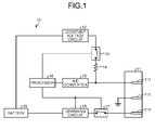
- FIG. 1 is a diagram of an exemplary hardware configuration of an electronic device according to a first embodiment.
- an electronic device 10 includes a micro USB connector 11, a constant voltage circuit 12, switches 13 and 17, a resistor 14, an analog/digital (A/D) converter 15, a processor 16, a charging circuit 18, and a battery 19.
- the micro USB connector 11 includes an ID terminal 111, a ground terminal 112, and a VBUS terminal 113.
- the micro USB connector 11 is a connector used for connecting an external device to the electronic device 10.
- the ID terminal 111 is a terminal used for identifying an external device.
- the VBUS terminal 113 is a terminal used for charging the battery 19.
- the constant voltage circuit 12 is connected to the ID terminal 111 via the switch 13 and the resistor 14.
- the constant voltage circuit 12 regulates the voltage supplied from the battery 19 so as to output a constant voltage.
- the constant voltage is supplied to the ID terminal 111 via the switch 13 and the resistor 14. For example, when the voltage supplied from the battery 19 fluctuates in the range from 3 to 4 volts [V] due to an influence of temperature or the like, the constant voltage circuit 12 outputs a constant voltage of 2.5 [V].
- the voltage at the resistor 14, i.e., the voltage at the ID terminal 111 is input to the A/D converter 15.
- the A/D converter 15 detects an analog voltage value.
- the A/D converter 15 converts the detected analog voltage value into a digital voltage value and outputs the digital voltage value to the processor 16.
- the resistor 14 has, without any change, the output voltage of the constant voltage circuit 12. Accordingly, the output voltage value of the constant voltage circuit 12 is detected by the A/D converter 15, as the voltage value at the ID terminal 111.
- the output voltage of the constant voltage circuit 12 is divided according to the ratio between the resistance value of the resistor 14 and the resistance value of the connection terminal of the external device.
- the divided voltage value at the resistor 14 is detected by the A/D converter 15 as the voltage value at the ID terminal 111.
- the micro USB connector 11 gets wet with water, a resistance component due to the water is generated between the ID terminal 111 and the ground terminal 112.
- the output voltage of the constant voltage circuit 12 is divided according to the ratio between the resistance value of the resistor 14 and the resistance value of the water. Accordingly, the divided voltage value at the resistor 14 is detected by the A/D converter 15 as the voltage value at the ID terminal 111.
- the processor 16 controls the switches 13 and 17. Before an external device is connected to the micro USB connector 11, the processor 16 has the switches 13 and 17 turned on. After an external device is connected to the micro USB connector 11, the processor 16 exercises control to turn the switches 13 and 17 on and off, in accordance with the voltage value input thereto by the A/D converter 15, i.e., the voltage value at the ID terminal 111. Further, the processor 16 controls operations of the charging circuit 18. The control exercised by the processor 16 will be explained in detail later. Examples of the processor 16 include a Central Processing Unit (CPU), a Digital Signal Processor (DSP), and a Field Programmable Gate Array (FPGA).
- CPU Central Processing Unit
- DSP Digital Signal Processor
- FPGA Field Programmable Gate Array
- the charging circuit 18 is connected to the VBUS terminal 113 via the switch 17. When a charging device is connected to the micro USB connector 11, the charging circuit 18 charges the battery 19 with the electric power supplied from the charging device via the VBUS terminal 113.
- FIG. 2 is a drawing for explaining operations of the electronic device according to the first embodiment.
- the vertical axis expresses the voltage value at the resistor 14, i.e., the voltage value at the ID terminal 111.
- the horizontal axis expresses a period of time that has elapsed since an external device is connected to the micro USB connector 11.
- Each of the measured results 21, 22, and 23 indicates fluctuation in the voltage that are observed when the micro USB connector 11 is wet with water.
- Each of the measured results 24 and 25 indicates fluctuation in the voltage that are observed when an external device is connected while the micro USB connector 11 is not wet with water.
- the voltage value at the ID terminal 111 exhibits a substantially constant value according to the resistance value of the connection terminal of the external device being connected, as indicated by the measured results 24 and 25.
- the resistance value of the connection terminal of the external device varies depending on the type of the external device.
- the range of variation in the resistance value is regulated by the Mobile Computing Promotion Consortium (MCPC) TR-014 specification, the CEA-936-A specification, a Battery Charging specification, or the like.
- MCPC Mobile Computing Promotion Consortium
- the voltage value at the ID terminal 111 is substantially constant within a range A of 1.5 ⁇ 0.1 [V].
- the voltage value at the ID terminal 111 is substantially constant within a range B of 0 to 0.1 [V].
- the voltage value at the ID terminal 111 fluctuates over the course of time as indicated by the measured results 21, 22, and 23.
- the resistance value of the water fluctuates in accordance with fluctuation of the ion concentration.
- the resistance value of the water is determined according to the state of the water such as the temperature of the water, the salinity concentration, the concentrations of other liquids contained in the water, and the concentration of impurities contained in the water.
- the voltage value at the ID terminal 111 is different for each of the measured results 21, 22, and 23, because the state of the water is also different for each of the measured results.
- the processor 16 monitors fluctuation in the voltage at the ID terminal 111. Further, when the fluctuation in the voltage during a predetermined time period are within a predetermined range, the processor 16 determines that the micro USB connector 11 is not in a wet state and electrically connects the micro USB connector 11. Further, when the fluctuation in the voltage during the predetermined time period are within the predetermined range, the processor 16 identifies the external device connected to the micro USB connector 11. On the contrary, when the fluctuation in the voltage during the predetermined time period are not within the predetermined range, the processor 16 determines that either the micro USB connector 11 is in a wet state or an external device that is not compliant with the specifications is connected, and the processor 16 electrically separates the micro USB connector 11.
- the processor 16 measures the voltage value at the ID terminal 111 eight times at intervals of 0.5 seconds between the time when the external device is connected to the micro USB connector 11 and 3.5 seconds later. Further, when all the eight measured values are either within the range A of 1.5 ⁇ 0.1 [V] or within the range B of 0 to 0.1 [V] as indicated by the measured results 24 and 25, the processor 16 keeps the switches 13 and 17 on. Further, when all the eight measured values are within the range A as indicated by the measured result 24, the processor 16 determines that the external device connected to the micro USB connector 11 is a charging device and causes the charging circuit 18 to operate. In contrast, when all the eight measured values are within the range B as indicated by the measured result 25, the processor 16 determines that the external device connected to the micro USB connector 11 is a USB memory.
- the processor 16 turns the switches 13 and 17 off.
- the processor 16 By turning the switch 17 off, because the current path between the VBUS terminal 113 and the charging circuit 18 is cut off, the processor 16 is able to arrange the switch 17 to block the current flowing into the electronic device 10 from the charging device via the VBUS terminal 113. As a result, even when the charging device is connected while the micro USB connector 11 is wet with water, it is possible to prevent a large amount of current from flowing into the electronic device 10. Thus, by electrically separating the micro USB connector 11 by turning the switch 17 off, it is possible to prevent failures of the electronic device 10 that may be caused by the micro USB connector 11 getting wet.
- the processor 16 is able to arrange the switch 13 to block the voltage supplied to the ID terminal 111 from the constant voltage circuit 12. As a result, it is possible to prevent the ID terminal 111 from being corroded by being wet with water.
- the switch 13 By electrically separating the micro USB connector 11 by turning the switch 13 off, it is possible to prevent failures of the electronic device 10 that may be caused by the micro USB connector 11 getting wet.
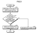
- FIG. 3 is a flowchart for explaining a process performed by the electronic device according to the first embodiment.
- the processor 16 monitors fluctuation in the voltage at the ID terminal 111, by measuring the voltage value at the ID terminal 111 plurality of times (n times) during a predetermined time period (step S31).
- the predetermined time period may be 3.5 seconds, while the number of times the measuring process is performed may be eight.
- the processor 16 judges whether the measured values from all of the measuring processes performed n times is within a predetermined range (step S32).
- the predetermined range may be, for example, either the range A or the range B illustrated in FIG. 2 .
- step S32 when all of the measured values from the measuring processes performed n times is within the predetermined range (step S32: Yes), the processor 16 identifies the external device connected to the micro USB connector 11 on the basis of the measured values (step S33).
- step S34 when at least one of the measured values from the measuring processes performed n times is not within the predetermined range (step S32: No), the processor 16 turns the switches 13 and 17 off (step S34).
- the processor 16 monitors the fluctuation in the voltage at the ID terminal 111 of the micro USB connector 11 in the electronic device 10. Further, when the fluctuation in the voltage at the ID terminal 111 during the predetermined time period are not within the predetermined range, the processor 16 electrically separates the micro USB connector 11.
- the processor 16 electrically separates the micro USB connector 11 so as to block the inflow current from the external device connected to the micro USB connector 11.
- the processor 16 electrically separates the micro USB connector 11 so as to stop the supply of the voltage to the ID terminal 111.
Landscapes
- Engineering & Computer Science (AREA)
- Signal Processing (AREA)
- Human Computer Interaction (AREA)
- Computer Networks & Wireless Communication (AREA)
- Power Sources (AREA)
- Telephone Function (AREA)
Abstract
Description
- The embodiments discussed herein are related to an electronic device, a voltage monitoring method, and a voltage monitoring program.
- As for a portable electronic device provided with a connector used for connecting an external device to the portable electronic device, when a charging device is connected to the connector while the connector is wet with water, a large amount of electric current (hereinafter, "current") flows into the portable electronic device, and a failure may occur in the electronic device. Thus, portable electronic devices are known with which a cap is provided for the opening of the connector, so as to prevent the connector from getting wet. However, the configuration where a cap is provided for the opening of the connector is troublesome.
- To cope with these situations, as a first piece of related-art, a configuration is known by which the power supply to a circuit within a portable electronic device is stopped when the portable electronic device is detected to be in a wet state, so as to prevent failures of the portable electronic device, without having to provide a cap for the opening of a connector.
- As a second piece of related-art, another configuration is also known in which a wet state of a portable electronic device is detected by detecting a short-circuit state of an existing terminal that is already provided in the portable electronic device, so as to be able to detect the wet state without having to enlarge the scale of the portable electronic device.
- Some portable electronic devices that are recently on the market are provided with a connector (which hereinafter may be referred to as a "micro USB connector") that is compliant with the micro USB specification, as a connector used for connecting an external device to the portable electronic device. Examples of terminals which a micro USB connector may have include: an "ID terminal", a "ground terminal", a "VBUS terminal". The voltage value detected at the ID terminal fluctuates according to the resistance value of a connection terminal of an external device connected to the micro USB connector. Thus, the portable electronic device is able to identify the external device connected to the micro USB connector, according to the voltage value detected at the ID terminal. For example, the portable electronic device determines that an "external device A" is connected to the micro USB connector when the voltage value at the ID terminal is "X volts [V]", whereas the portable electronic device determines that an "external device B" is connected to the micro USB connector when the voltage value at the ID terminal is "Y [V]".
- Related-art examples are described, for example, Japanese Laid-open Patent Publication No.
2004-235724 2010-035036 - The voltage value at the ID terminal, however, not only fluctuates according to the external device connected to the micro USB connector, but also fluctuates when the micro USB connector gets wet with water. The reason is that a resistance value due to the water is generated between the ID terminal and the ground terminal when the micro USB connector gets wet with water. When the voltage value detected at the ID terminal when the micro USB connector is in a wet state happens to coincide with a voltage value corresponding to a specific external device, the portable electronic device mistakenly recognizes the wet state as a state where the specific external device is connected. Even when a charging device is connected as an external device while the micro USB connector is wet with water, when the portable electronic device is able to accurately detect the wet state, it will be possible to block the current flowing into the portable electronic device from the charging device. However, when the portable electronic device mistakenly recognizes the wet state as a state where a charging device is connected, a large amount of current will flow into the portable electronic device, and a failure may occur in the portable electronic device.
- Accordingly, it is desirable in one aspect of an embodiment of the invention to prevent failures caused by a connector getting wet.
- According to an embodiment of one aspect of the invention, an electronic device includes a processor, and a connector used for connecting an external device to the electronic device, wherein the processor monitors fluctuation in a voltage at a specific terminal of the connector, and when the fluctuation in the voltage during a predetermined time period are not within a predetermined range, the processor electrically separates the connector.
-
-
FIG. 1 is a diagram of an exemplary hardware configuration of an electronic device according to a first embodiment; -
FIG. 2 is a drawing for explaining operations of the electronic device according to the first embodiment; and -
FIG. 3 is a flowchart for explaining a process performed by the electronic device according to the first embodiment. - Preferred embodiments of the present invention will be explained, by way of example only, with reference to accompanying drawings.
- The electronic device, the voltage monitoring method, and the voltage monitoring program of the present disclosure are not limited to the exemplary embodiments.
- The electronic device of the present disclosure may be a portable electronic device such as a smartphone, a tablet terminal device, or the like or may be a stationary electronic device such as a desktop personal computer or the like.
-
FIG. 1 is a diagram of an exemplary hardware configuration of an electronic device according to a first embodiment. InFIG. 1 , anelectronic device 10 includes amicro USB connector 11, a constant voltage circuit 12,switches resistor 14, an analog/digital (A/D)converter 15, a processor 16, acharging circuit 18, and a battery 19. Further, themicro USB connector 11 includes anID terminal 111, aground terminal 112, and aVBUS terminal 113. Themicro USB connector 11 is a connector used for connecting an external device to theelectronic device 10. TheID terminal 111 is a terminal used for identifying an external device. The VBUSterminal 113 is a terminal used for charging the battery 19. - The constant voltage circuit 12 is connected to the
ID terminal 111 via theswitch 13 and theresistor 14. The constant voltage circuit 12 regulates the voltage supplied from the battery 19 so as to output a constant voltage. The constant voltage is supplied to theID terminal 111 via theswitch 13 and theresistor 14. For example, when the voltage supplied from the battery 19 fluctuates in the range from 3 to 4 volts [V] due to an influence of temperature or the like, the constant voltage circuit 12 outputs a constant voltage of 2.5 [V]. - The voltage at the
resistor 14, i.e., the voltage at theID terminal 111 is input to the A/D converter 15. Thus, the A/D converter 15 detects an analog voltage value. The A/D converter 15 converts the detected analog voltage value into a digital voltage value and outputs the digital voltage value to the processor 16. - In this situation, when no external device is connected to the
micro USB connector 11, theresistor 14 has, without any change, the output voltage of the constant voltage circuit 12. Accordingly, the output voltage value of the constant voltage circuit 12 is detected by the A/D converter 15, as the voltage value at theID terminal 111. - In contrast, when an external device is connected to the
micro USB connector 11, the output voltage of the constant voltage circuit 12 is divided according to the ratio between the resistance value of theresistor 14 and the resistance value of the connection terminal of the external device. Thus, the divided voltage value at theresistor 14 is detected by the A/D converter 15 as the voltage value at theID terminal 111. - Further, when the
micro USB connector 11 gets wet with water, a resistance component due to the water is generated between theID terminal 111 and theground terminal 112. Thus, the output voltage of the constant voltage circuit 12 is divided according to the ratio between the resistance value of theresistor 14 and the resistance value of the water. Accordingly, the divided voltage value at theresistor 14 is detected by the A/D converter 15 as the voltage value at theID terminal 111. - The processor 16 controls the
switches micro USB connector 11, the processor 16 has theswitches micro USB connector 11, the processor 16 exercises control to turn theswitches D converter 15, i.e., the voltage value at theID terminal 111. Further, the processor 16 controls operations of thecharging circuit 18. The control exercised by the processor 16 will be explained in detail later. Examples of the processor 16 include a Central Processing Unit (CPU), a Digital Signal Processor (DSP), and a Field Programmable Gate Array (FPGA). - The
charging circuit 18 is connected to the VBUSterminal 113 via theswitch 17. When a charging device is connected to themicro USB connector 11, thecharging circuit 18 charges the battery 19 with the electric power supplied from the charging device via theVBUS terminal 113. Operations of the electronic deviceFIG. 2 is a drawing for explaining operations of the electronic device according to the first embodiment. InFIG. 2 , the vertical axis expresses the voltage value at theresistor 14, i.e., the voltage value at theID terminal 111. The horizontal axis expresses a period of time that has elapsed since an external device is connected to themicro USB connector 11. - Each of the measured
results micro USB connector 11 is wet with water. Each of the measuredresults micro USB connector 11 is not wet with water. - When an external device is connected while the
micro USB connector 11 is not wet with water, the voltage value at theID terminal 111 exhibits a substantially constant value according to the resistance value of the connection terminal of the external device being connected, as indicated by the measuredresults micro USB connector 11 is a charging device, the voltage value at theID terminal 111 is substantially constant within a range A of 1.5±0.1 [V]. As another example, when the external device connected to themicro USB connector 11 is a USB memory, the voltage value at theID terminal 111 is substantially constant within a range B of 0 to 0.1 [V]. - In contrast, when the
micro USB connector 11 is wet with water, the voltage value at theID terminal 111 fluctuates over the course of time as indicated by the measuredresults ID terminal 111 fluctuates over the course of time due to an influence of the voltage supplied to theID terminal 111, the resistance value of the water fluctuates in accordance with fluctuation of the ion concentration. Further, the resistance value of the water is determined according to the state of the water such as the temperature of the water, the salinity concentration, the concentrations of other liquids contained in the water, and the concentration of impurities contained in the water. The voltage value at theID terminal 111 is different for each of the measuredresults - Accordingly, the processor 16 monitors fluctuation in the voltage at the
ID terminal 111. Further, when the fluctuation in the voltage during a predetermined time period are within a predetermined range, the processor 16 determines that themicro USB connector 11 is not in a wet state and electrically connects themicro USB connector 11. Further, when the fluctuation in the voltage during the predetermined time period are within the predetermined range, the processor 16 identifies the external device connected to themicro USB connector 11. On the contrary, when the fluctuation in the voltage during the predetermined time period are not within the predetermined range, the processor 16 determines that either themicro USB connector 11 is in a wet state or an external device that is not compliant with the specifications is connected, and the processor 16 electrically separates themicro USB connector 11. - For example, as illustrated in
FIG. 2 , the processor 16 measures the voltage value at theID terminal 111 eight times at intervals of 0.5 seconds between the time when the external device is connected to themicro USB connector 11 and 3.5 seconds later. Further, when all the eight measured values are either within the range A of 1.5±0.1 [V] or within the range B of 0 to 0.1 [V] as indicated by the measuredresults switches result 24, the processor 16 determines that the external device connected to themicro USB connector 11 is a charging device and causes the chargingcircuit 18 to operate. In contrast, when all the eight measured values are within the range B as indicated by the measuredresult 25, the processor 16 determines that the external device connected to themicro USB connector 11 is a USB memory. - On the contrary, when at least one of the eight measured values is neither within the range A nor within the range B, i.e., when the fluctuation in the voltage at the
ID terminal 111 during the predetermined time period are not within the predetermined range, as indicated by the measuredresults switches - By turning the
switch 17 off, because the current path between theVBUS terminal 113 and the chargingcircuit 18 is cut off, the processor 16 is able to arrange theswitch 17 to block the current flowing into theelectronic device 10 from the charging device via theVBUS terminal 113. As a result, even when the charging device is connected while themicro USB connector 11 is wet with water, it is possible to prevent a large amount of current from flowing into theelectronic device 10. Thus, by electrically separating themicro USB connector 11 by turning theswitch 17 off, it is possible to prevent failures of theelectronic device 10 that may be caused by themicro USB connector 11 getting wet. - Further, when a voltage keeps being supplied to the
ID terminal 111 while theID terminal 111 remains wet with water, a chemical reaction is caused by the water on theID terminal 111, and theID terminal 111 may corrode. The corrosion of theID terminal 111 is one of the factors that can cause a failure of theelectronic device 10. To cope with this situation, by turning theswitch 13 off, the processor 16 is able to arrange theswitch 13 to block the voltage supplied to theID terminal 111 from the constant voltage circuit 12. As a result, it is possible to prevent theID terminal 111 from being corroded by being wet with water. Thus, by electrically separating themicro USB connector 11 by turning theswitch 13 off, it is possible to prevent failures of theelectronic device 10 that may be caused by themicro USB connector 11 getting wet. -
FIG. 3 is a flowchart for explaining a process performed by the electronic device according to the first embodiment. - When an external device is connected to the
micro USB connector 11, the processor 16 monitors fluctuation in the voltage at theID terminal 111, by measuring the voltage value at theID terminal 111 plurality of times (n times) during a predetermined time period (step S31). For example, as illustrated inFIG. 2 , the predetermined time period may be 3.5 seconds, while the number of times the measuring process is performed may be eight. - Subsequently, the processor 16 judges whether the measured values from all of the measuring processes performed n times is within a predetermined range (step S32). The predetermined range may be, for example, either the range A or the range B illustrated in
FIG. 2 . - After that, when all of the measured values from the measuring processes performed n times is within the predetermined range (step S32: Yes), the processor 16 identifies the external device connected to the
micro USB connector 11 on the basis of the measured values (step S33). - On the contrary, when at least one of the measured values from the measuring processes performed n times is not within the predetermined range (step S32: No), the processor 16 turns the
switches - As explained above, according to the first embodiment, the processor 16 monitors the fluctuation in the voltage at the
ID terminal 111 of themicro USB connector 11 in theelectronic device 10. Further, when the fluctuation in the voltage at theID terminal 111 during the predetermined time period are not within the predetermined range, the processor 16 electrically separates themicro USB connector 11. - When the fluctuation in the voltage during the predetermined time period are within the predetermined range, it is possible to determine that
micro USB connector 11 is not in a wet state. On the contrary, when the fluctuation in the voltage during the predetermined time period are not within the predetermined range, there is a possibility that themicro USB connector 11 is in a wet state. Thus, by electrically separating themicro USB connector 11 when the fluctuation in the voltage during the predetermined time period are not within the predetermined range, it is possible to prevent failures of theelectronic device 10 that may be caused by themicro USB connector 11 getting wet. - Further, the processor 16 electrically separates the
micro USB connector 11 so as to block the inflow current from the external device connected to themicro USB connector 11. - Thus, even when a charging device is connected while the
micro USB connector 11 is wet with water, it is possible to prevent a large amount of current from flowing into theelectronic device 10. Consequently, it is possible to prevent failures of theelectronic device 10 that may be caused by an inflow of a large amount of current. The inflow current from the external device is blocked as a result of the processor 16 turning theswitch 17 off. - Further, the processor 16 electrically separates the
micro USB connector 11 so as to stop the supply of the voltage to theID terminal 111. - With this arrangement, it is possible to prevent the
ID terminal 111 that is wet with water from corroding. Consequently, it is possible to prevent failures of theelectronic device 10 that may be caused by corrosions of theID terminal 111. The supply of the voltage to theID terminal 111 is stopped as a result of the processor 16 turning theswitch 13 off. -
- (1) The processes described above performed by the processor 16 may be realized by causing the processor 16 to execute a computer program (hereinafter, "program") corresponding to the processes. For example, the program corresponding to the processes described above performed by the processor 16 may be stored in a memory (not depicted) included in the
electronic device 10 so that the program is read from the memory and executed by the processor 16. - (2) In the exemplary embodiment described above, both the
switches micro USB connector 11. However, another arrangement is also acceptable in which only one of theswitches micro USB connector 11. When theswitch 13 is turned off, themicro USB connector 11 is electrically separated at theID terminal 111. In contrast, when theswitch 17 is turned off, themicro USB connector 11 is electrically separated at theVBUS terminal 113. - (3) In the exemplary embodiment described above, the
micro USB connector 11 is presented as an example of the connector used for connecting an external device. However, the connector used for connecting an external device does not necessarily have to be themicro USB connector 11. The connector used for connecting an external device may be any device as long as the device has at least either a terminal to which a constant level of voltage is supplied from the electronic device or a terminal used for charging the power for the electronic device. - According to an aspect of an embodiment of the present disclosure, it is possible to prevent the failures that may be caused by the connector getting wet.
Claims (5)
- An electronic device (10) comprising:a processor (16); anda connector (11) used for connecting an external device to the electronic device (10), wherein
the processor (16) monitors fluctuation in a voltage at a specific terminal (111) of the connector (11), and
when the fluctuation in the voltage during a predetermined time period are not within a predetermined range, the processor (16) electrically separates the connector (11). - The electronic device (10) according to claim 1, wherein the processor (16) electrically separates the connector (11) so as to block an inflow of electric current from the external device connected to the connector (11).
- The electronic device according to claim 1 or 2, wherein the processor (16) electrically separates the connector (11) so as to stop a supply of a voltage to the specific terminal (111).
- A voltage monitoring method implemented for an electronic device that includes a connector used for connecting an external device to the electronic device, the voltage monitoring method comprising:monitoring fluctuation in a voltage at a specific terminal of the connector; andelectrically separating the connector when the fluctuation in the voltage during a predetermined time period are not within a predetermined range.
- A voltage monitoring program used by an electronic device (10) that includes a processor (16) and a connector (11) used for connecting an external device to the electronic device (10), the voltage monitoring program causing the processor (16) to execute:monitoring fluctuation in a voltage at a specific terminal (111) of the connector (11); andelectrically separating the connector (11) when the fluctuation in the voltage during a predetermined time period are not within a predetermined range.
Applications Claiming Priority (1)
| Application Number | Priority Date | Filing Date | Title |
|---|---|---|---|
| JP2013168744A JP2015037269A (en) | 2013-08-14 | 2013-08-14 | Electronic device, voltage monitoring method and voltage monitoring program |
Publications (1)
| Publication Number | Publication Date |
|---|---|
| EP2843914A1 true EP2843914A1 (en) | 2015-03-04 |
Family
ID=51257336
Family Applications (1)
| Application Number | Title | Priority Date | Filing Date |
|---|---|---|---|
| EP14178920.6A Withdrawn EP2843914A1 (en) | 2013-08-14 | 2014-07-29 | Electronic device and voltage monitoring method |
Country Status (3)
| Country | Link |
|---|---|
| US (1) | US9490625B2 (en) |
| EP (1) | EP2843914A1 (en) |
| JP (1) | JP2015037269A (en) |
Cited By (2)
| Publication number | Priority date | Publication date | Assignee | Title |
|---|---|---|---|---|
| CN106200790A (en) * | 2016-06-30 | 2016-12-07 | 联想(北京)有限公司 | A kind of information processing method and electronic equipment |
| EP3617842A4 (en) * | 2017-05-16 | 2020-05-06 | SONY Corporation | INFORMATION PROCESSING DEVICE, CONTROL CIRCUIT, AND INFORMATION PROCESSING METHOD |
Families Citing this family (15)
| Publication number | Priority date | Publication date | Assignee | Title |
|---|---|---|---|---|
| US11458851B2 (en) * | 2014-07-03 | 2022-10-04 | The Noco Company | Jump starting apparatus |
| JP6424141B2 (en) * | 2015-06-01 | 2018-11-14 | 富士通クライアントコンピューティング株式会社 | Electronic device, control program, and control method |
| JP6743430B2 (en) * | 2016-03-11 | 2020-08-19 | マックス株式会社 | Battery pack |
| US10236683B2 (en) * | 2016-06-10 | 2019-03-19 | Apple Inc. | Corrosion mitigation for an external connector of an electronic device |
| KR102675073B1 (en) | 2016-07-12 | 2024-06-14 | 삼성전자주식회사 | Electronic device supporting usb interface and control method for the usb interface |
| JP6820077B2 (en) * | 2016-08-18 | 2021-01-27 | 富士通コネクテッドテクノロジーズ株式会社 | Short circuit judgment method and electronic equipment |
| JP6835434B2 (en) * | 2016-12-01 | 2021-02-24 | 富士通コネクテッドテクノロジーズ株式会社 | Electronics |
| EP3932316B1 (en) | 2017-03-30 | 2023-08-02 | Koninklijke Philips N.V. | Intravascular ultrasound patient interface module (pim) for distributed wireless intraluminal imaging systems |
| JP7047447B2 (en) * | 2018-02-19 | 2022-04-05 | セイコーエプソン株式会社 | Audio output circuit and projector |
| CN108399142B (en) * | 2018-03-20 | 2021-06-01 | 青岛海信移动通信技术股份有限公司 | USB interface circuit and mobile terminal |
| US10837934B2 (en) * | 2018-03-28 | 2020-11-17 | Samsung Electronics Co., Ltd. | Water detection circuit, electronic device including the same, and water detection method |
| JP7284377B2 (en) * | 2019-01-30 | 2023-05-31 | アイコム株式会社 | Electronics |
| KR102888556B1 (en) | 2020-03-24 | 2025-11-21 | 삼성메디슨 주식회사 | Ultrasonic probe, ultrasonic imaging device and controlling method thereof |
| US11658443B2 (en) | 2021-04-13 | 2023-05-23 | Apple Inc. | Liquid detection and corrosion mitigation |
| JP2025074565A (en) * | 2023-10-30 | 2025-05-14 | パナソニックIpマネジメント株式会社 | Wiring devices that supply power |
Citations (4)
| Publication number | Priority date | Publication date | Assignee | Title |
|---|---|---|---|---|
| JP2004235724A (en) | 2003-01-28 | 2004-08-19 | Nec Saitama Ltd | Structure and method for detecting water leak of electronic apparatus |
| JP2010035036A (en) | 2008-07-30 | 2010-02-12 | Kyocera Corp | Mobile electronic device |
| US20100259399A1 (en) * | 2009-04-10 | 2010-10-14 | Kabushiki Kaisha Toshiba | Mobile communication device configured to sense external cable |
| US20110050175A1 (en) * | 2009-08-31 | 2011-03-03 | Lenovo (Singapore) Pte. Ltd. | Battery Pack |
Family Cites Families (6)
| Publication number | Priority date | Publication date | Assignee | Title |
|---|---|---|---|---|
| JP3819658B2 (en) * | 1999-12-27 | 2006-09-13 | 三洋電機株式会社 | Portable electronic devices with a common serial bus connector |
| US7679317B2 (en) * | 2005-02-15 | 2010-03-16 | Research In Motion Limited | Systems and methods for charging a chargeable USB device |
| JP2008305148A (en) * | 2007-06-07 | 2008-12-18 | Kenwood Corp | Usb power supply booster |
| JP2012209902A (en) * | 2011-03-30 | 2012-10-25 | Semiconductor Components Industries Llc | Input and output circuit |
| JP2012222858A (en) * | 2011-04-04 | 2012-11-12 | Panasonic Corp | Portable information device, electronic device, and connection detection mechanism |
| JP2013019739A (en) * | 2011-07-11 | 2013-01-31 | Nec Casio Mobile Communications Ltd | Connector abnormality detector, connector abnormality detection system, and program |
-
2013
- 2013-08-14 JP JP2013168744A patent/JP2015037269A/en active Pending
-
2014
- 2014-07-24 US US14/339,852 patent/US9490625B2/en not_active Expired - Fee Related
- 2014-07-29 EP EP14178920.6A patent/EP2843914A1/en not_active Withdrawn
Patent Citations (4)
| Publication number | Priority date | Publication date | Assignee | Title |
|---|---|---|---|---|
| JP2004235724A (en) | 2003-01-28 | 2004-08-19 | Nec Saitama Ltd | Structure and method for detecting water leak of electronic apparatus |
| JP2010035036A (en) | 2008-07-30 | 2010-02-12 | Kyocera Corp | Mobile electronic device |
| US20100259399A1 (en) * | 2009-04-10 | 2010-10-14 | Kabushiki Kaisha Toshiba | Mobile communication device configured to sense external cable |
| US20110050175A1 (en) * | 2009-08-31 | 2011-03-03 | Lenovo (Singapore) Pte. Ltd. | Battery Pack |
Cited By (6)
| Publication number | Priority date | Publication date | Assignee | Title |
|---|---|---|---|---|
| CN106200790A (en) * | 2016-06-30 | 2016-12-07 | 联想(北京)有限公司 | A kind of information processing method and electronic equipment |
| CN106200790B (en) * | 2016-06-30 | 2020-03-24 | 联想(北京)有限公司 | Information processing method and electronic equipment |
| EP3617842A4 (en) * | 2017-05-16 | 2020-05-06 | SONY Corporation | INFORMATION PROCESSING DEVICE, CONTROL CIRCUIT, AND INFORMATION PROCESSING METHOD |
| US11482188B2 (en) | 2017-05-16 | 2022-10-25 | Sony Corporation | Information processing device, control circuit, and information processing method |
| US11682363B2 (en) | 2017-05-16 | 2023-06-20 | Sony Group Corporation | Information processing device, control circuit, and information processing method |
| US12400619B2 (en) | 2017-05-16 | 2025-08-26 | Sony Group Corporation | Information processing device, control circuit, and information processing method |
Also Published As
| Publication number | Publication date |
|---|---|
| JP2015037269A (en) | 2015-02-23 |
| US9490625B2 (en) | 2016-11-08 |
| US20150049407A1 (en) | 2015-02-19 |
Similar Documents
| Publication | Publication Date | Title |
|---|---|---|
| EP2843914A1 (en) | Electronic device and voltage monitoring method | |
| US11095119B2 (en) | Corrosion mitigation for an external connector of an electronic device | |
| EP3451487B1 (en) | Power adapter, terminal, and method for processing impedance anomalies in charging loop | |
| US9246342B2 (en) | Charging system for portable electronic equipment | |
| US10128682B2 (en) | Charger for electric vehicles | |
| US20160169980A1 (en) | Method and Apparatus for Contact Detection in Battery Packs | |
| US10291044B2 (en) | Battery charger and control method thereof | |
| TW201606328A (en) | Battery residual prediction device and battery pack | |
| US10741348B2 (en) | Power transmission apparatus | |
| EP3279656B1 (en) | Apparatus and methods for reducing electrical shock hazard from biosensor meters | |
| CN108093118B (en) | Method and device for testing devices on mainboard and computer readable storage medium | |
| JP6272379B2 (en) | Cable inspection device and cable inspection system | |
| JP6710574B2 (en) | Short detection circuit | |
| CN115575452B (en) | Liquid inlet detection circuit and electronic equipment | |
| CN111431221B (en) | Charging device, resistance detection method and circuit | |
| JP5830458B2 (en) | Electronic control unit | |
| JP6225486B2 (en) | Cell voltage measuring device | |
| JP6608234B2 (en) | Contact determination device and measurement device | |
| US9912180B2 (en) | Charge device for battery charging and method thereof | |
| JP2015175759A (en) | current measuring device | |
| JP2018189534A (en) | Wire inspection device | |
| US11114705B2 (en) | Current measurement and voltage control approach | |
| CN223436936U (en) | Battery-removable devices and virtual reality devices | |
| JP2016103444A (en) | Battery monitoring apparatus | |
| JP2007248139A (en) | Tracking short-circuit detection method |
Legal Events
| Date | Code | Title | Description |
|---|---|---|---|
| 17P | Request for examination filed |
Effective date: 20140729 |
|
| AK | Designated contracting states |
Kind code of ref document: A1 Designated state(s): AL AT BE BG CH CY CZ DE DK EE ES FI FR GB GR HR HU IE IS IT LI LT LU LV MC MK MT NL NO PL PT RO RS SE SI SK SM TR |
|
| AX | Request for extension of the european patent |
Extension state: BA ME |
|
| PUAI | Public reference made under article 153(3) epc to a published international application that has entered the european phase |
Free format text: ORIGINAL CODE: 0009012 |
|
| R17P | Request for examination filed (corrected) |
Effective date: 20150804 |
|
| RBV | Designated contracting states (corrected) |
Designated state(s): AL AT BE BG CH CY CZ DE DK EE ES FI FR GB GR HR HU IE IS IT LI LT LU LV MC MK MT NL NO PL PT RO RS SE SI SK SM TR |
|
| STAA | Information on the status of an ep patent application or granted ep patent |
Free format text: STATUS: THE APPLICATION HAS BEEN WITHDRAWN |
|
| 18W | Application withdrawn |
Effective date: 20180110 |