EP2843864A1 - Systems and methods for multiple sensor noise predictive filtering - Google Patents
Systems and methods for multiple sensor noise predictive filtering Download PDFInfo
- Publication number
- EP2843864A1 EP2843864A1 EP14173913.6A EP14173913A EP2843864A1 EP 2843864 A1 EP2843864 A1 EP 2843864A1 EP 14173913 A EP14173913 A EP 14173913A EP 2843864 A1 EP2843864 A1 EP 2843864A1
- Authority
- EP
- European Patent Office
- Prior art keywords
- data
- circuit
- data input
- operable
- output
- Prior art date
- Legal status (The legal status is an assumption and is not a legal conclusion. Google has not performed a legal analysis and makes no representation as to the accuracy of the status listed.)
- Granted
Links
Images



Classifications
-
- G—PHYSICS
- G06—COMPUTING OR CALCULATING; COUNTING
- G06F—ELECTRIC DIGITAL DATA PROCESSING
- G06F9/00—Arrangements for program control, e.g. control units
- G06F9/06—Arrangements for program control, e.g. control units using stored programs, i.e. using an internal store of processing equipment to receive or retain programs
- G06F9/46—Multiprogramming arrangements
-
- H—ELECTRICITY
- H03—ELECTRONIC CIRCUITRY
- H03M—CODING; DECODING; CODE CONVERSION IN GENERAL
- H03M13/00—Coding, decoding or code conversion, for error detection or error correction; Coding theory basic assumptions; Coding bounds; Error probability evaluation methods; Channel models; Simulation or testing of codes
- H03M13/63—Joint error correction and other techniques
- H03M13/6331—Error control coding in combination with equalisation
-
- H—ELECTRICITY
- H03—ELECTRONIC CIRCUITRY
- H03M—CODING; DECODING; CODE CONVERSION IN GENERAL
- H03M13/00—Coding, decoding or code conversion, for error detection or error correction; Coding theory basic assumptions; Coding bounds; Error probability evaluation methods; Channel models; Simulation or testing of codes
- H03M13/63—Joint error correction and other techniques
- H03M13/6343—Error control coding in combination with techniques for partial response channels, e.g. recording
-
- G—PHYSICS
- G11—INFORMATION STORAGE
- G11B—INFORMATION STORAGE BASED ON RELATIVE MOVEMENT BETWEEN RECORD CARRIER AND TRANSDUCER
- G11B20/00—Signal processing not specific to the method of recording or reproducing; Circuits therefor
- G11B20/10—Digital recording or reproducing
- G11B20/10009—Improvement or modification of read or write signals
-
- G—PHYSICS
- G11—INFORMATION STORAGE
- G11B—INFORMATION STORAGE BASED ON RELATIVE MOVEMENT BETWEEN RECORD CARRIER AND TRANSDUCER
- G11B5/00—Recording by magnetisation or demagnetisation of a record carrier; Reproducing by magnetic means; Record carriers therefor
- G11B5/02—Recording, reproducing, or erasing methods; Read, write or erase circuits therefor
- G11B5/027—Analogue recording
- G11B5/035—Equalising
-
- G—PHYSICS
- G11—INFORMATION STORAGE
- G11B—INFORMATION STORAGE BASED ON RELATIVE MOVEMENT BETWEEN RECORD CARRIER AND TRANSDUCER
- G11B5/00—Recording by magnetisation or demagnetisation of a record carrier; Reproducing by magnetic means; Record carriers therefor
- G11B5/02—Recording, reproducing, or erasing methods; Read, write or erase circuits therefor
- G11B5/09—Digital recording
-
- H—ELECTRICITY
- H03—ELECTRONIC CIRCUITRY
- H03M—CODING; DECODING; CODE CONVERSION IN GENERAL
- H03M13/00—Coding, decoding or code conversion, for error detection or error correction; Coding theory basic assumptions; Coding bounds; Error probability evaluation methods; Channel models; Simulation or testing of codes
- H03M13/03—Error detection or forward error correction by redundancy in data representation, i.e. code words containing more digits than the source words
- H03M13/05—Error detection or forward error correction by redundancy in data representation, i.e. code words containing more digits than the source words using block codes, i.e. a predetermined number of check bits joined to a predetermined number of information bits
- H03M13/11—Error detection or forward error correction by redundancy in data representation, i.e. code words containing more digits than the source words using block codes, i.e. a predetermined number of check bits joined to a predetermined number of information bits using multiple parity bits
- H03M13/1102—Codes on graphs and decoding on graphs, e.g. low-density parity check [LDPC] codes
-
- H—ELECTRICITY
- H03—ELECTRONIC CIRCUITRY
- H03M—CODING; DECODING; CODE CONVERSION IN GENERAL
- H03M13/00—Coding, decoding or code conversion, for error detection or error correction; Coding theory basic assumptions; Coding bounds; Error probability evaluation methods; Channel models; Simulation or testing of codes
- H03M13/03—Error detection or forward error correction by redundancy in data representation, i.e. code words containing more digits than the source words
- H03M13/05—Error detection or forward error correction by redundancy in data representation, i.e. code words containing more digits than the source words using block codes, i.e. a predetermined number of check bits joined to a predetermined number of information bits
- H03M13/13—Linear codes
- H03M13/15—Cyclic codes, i.e. cyclic shifts of codewords produce other codewords, e.g. codes defined by a generator polynomial, Bose-Chaudhuri-Hocquenghem [BCH] codes
- H03M13/151—Cyclic codes, i.e. cyclic shifts of codewords produce other codewords, e.g. codes defined by a generator polynomial, Bose-Chaudhuri-Hocquenghem [BCH] codes using error location or error correction polynomials
- H03M13/1515—Reed-Solomon codes
-
- H—ELECTRICITY
- H03—ELECTRONIC CIRCUITRY
- H03M—CODING; DECODING; CODE CONVERSION IN GENERAL
- H03M13/00—Coding, decoding or code conversion, for error detection or error correction; Coding theory basic assumptions; Coding bounds; Error probability evaluation methods; Channel models; Simulation or testing of codes
- H03M13/37—Decoding methods or techniques, not specific to the particular type of coding provided for in groups H03M13/03 - H03M13/35
- H03M13/39—Sequence estimation, i.e. using statistical methods for the reconstruction of the original codes
- H03M13/41—Sequence estimation, i.e. using statistical methods for the reconstruction of the original codes using the Viterbi algorithm or Viterbi processors
-
- H—ELECTRICITY
- H04—ELECTRIC COMMUNICATION TECHNIQUE
- H04L—TRANSMISSION OF DIGITAL INFORMATION, e.g. TELEGRAPHIC COMMUNICATION
- H04L1/00—Arrangements for detecting or preventing errors in the information received
- H04L1/004—Arrangements for detecting or preventing errors in the information received by using forward error control
- H04L1/0045—Arrangements at the receiver end
- H04L1/0047—Decoding adapted to other signal detection operation
- H04L1/005—Iterative decoding, including iteration between signal detection and decoding operation
Definitions
- the present invention is related to systems and methods for branch metric calculation based on multiple data streams in a data processing circuit.
- the present invention is related to systems and methods for branch metric calculation based on multiple data streams in a data processing circuit. According to a first aspect of the invention, there is provided a data processing system as set out in claim 1.
- Various embodiments of the present invention provide data processing systems that include: a first multi-stream noise predictive filter circuit operable to generate a first interim output corresponding to a first data input based upon a non-matrix based combination of the first data input and a previous instance of a second data input; a second multi-stream noise predictive filter circuit operable to generate a second interim output corresponding to the second data input based upon a non-matrix based combination of the second data input and a previous instance of the first data input; and a combining circuit operable to combine at least the first interim output with the second interim output to yield a combination branch metric.
- the data processing system further comprises: a data detector circuit including the first multi-stream noise predictive filter circuit and the second multi-stream noise predictive filter circuit, and operable to provide a detected output corresponding to the first data input and the second data input based at least in part on the combination branch metric.
- the data processing system further comprises: a data decoder circuit operable to apply a data decode algorithm to the detected output to recover an original data set corresponding to the first data input and the second data input.
- the data decode algorithm is a low density parity check algorithm.
- the data detector circuit applies a Viterbi algorithm data detection.
- operation of the first multi-stream noise predictive filter circuit is based at least in part on a first coefficient set
- operation of the second multi-stream noise predictive filter circuit is based at least in part on a second coefficient set
- the system further comprises: a calibration circuit operable to: generate the first coefficient set based upon a difference between the first data input and an ideal first data input, and generate the second coefficient set based upon a difference between the second data input and an ideal second data input.
- the combining circuit is a summation circuit operable to sum the first interim output with at least the second interim output to yield the combination branch metric.
- generating the first interim output is done using a first linear computation, and wherein generating the second interim output is done using a second linear computation.
- the data processing system is implemented as part of a storage device including: a storage medium having at least a first track and a second track; and wherein a combination of the first data input and the second data input are selected from a group consisting of: a first data input and a second data input derived from the first track; and a first data input derived from the first track and the second data input derived from the second track.
- the data processing system is implemented as part of a storage device including a storage medium having tracks, wherein the first data input corresponds to a first sample location along a particular one of the tracks, wherein the second data input corresponds to a second sample location along the particular one of the tracks, and wherein the first sample location and the second sample location are sampled at the same sample time.
- the data processing system is implemented as part of an integrated circuit.
- a method comprising: generating a first interim output corresponding to a first data input using a first multi-stream noise predictive filter circuit based upon a non-matrix based combination of the first data input and a previous instance of a second data input; generating a second interim output corresponding to a second data input using a second multi-stream noise predictive filter circuit based upon a non-matrix based combination of the first data input and a previous instance of a second data input; and summing the first interim output with at least the second interim output to yield a combination branch metric.
- the method further comprises: applying a data detection algorithm relying on the combination branch metric to yield a detected output.
- a storage device comprising: a storage medium; a head assembly disposed in relation to the storage medium and operable to provide a first sensed signal and a second sensed signal corresponding to information along a track of the storage medium; a read channel circuit including: an analog front end circuit operable to provide a first analog signal corresponding to the first sensed signal, and a second analog signal corresponding to the second sensed signal; an analog to digital converter circuit operable to sample the first analog signal to yield a first series of digital samples, and sample the second analog signal to yield a second series of digital samples; an equalizer circuit operable to equalize the first series of digital samples to yield a first sample set, and equalize the second series of digital samples to yield a second sample set; a data detector circuit including: a first multi-stream noise predictive filter circuit operable to generate a first interim output corresponding to the first sample set based upon a non-matrix based combination of the first sample set and corresponding previous instances of the second sample
- the read channel circuit further comprises: a data decoder circuit operable to apply a data decode algorithm to the detected output to recover an original data set corresponding to the first sample set and the second sample set.
- the data decode algorithm is a low density parity check algorithm.
- the data detector circuit applies a Viterbi algorithm data detection.
- operation of the first multi-stream noise predictive filter circuit is based at least in part on a first coefficient set
- operation of the second multi-stream noise predictive filter circuit is based at least in part on a second coefficient set
- the system further comprises: a calibration circuit operable to: generate the first coefficient set based upon a difference between the first sample set and corresponding instances of an ideal first sample set, and generate the second coefficient set based upon a difference between the first sample set and corresponding instances of an ideal first sample set.
- generating the first interim output is done using a first linear computation, and wherein generating the second interim output is done using a second linear computation.
- the combining circuit is a summation circuit operable to sum the first interim output with at least the second interim output to yield the combination branch metric.
- Fig. 1a-1d depicts a data processing circuit having multiple stream noise filtering circuitry in accordance with some embodiments of the present invention
- Figs. 2a-2b are flow diagrams showing a method in accordance with some embodiments of the present invention for data processing using multiple stream noise filtering
- Fig. 3 shows a storage device including a read channel having multiple stream noise filtering circuitry in accordance with one or more embodiments of the present invention.
- the present invention is related to systems and methods for performing data processing, and more specifically to systems and methods for adaptive parameter modification in a data processing system.
- Various embodiments of the present invention provide data processing circuits that include a data detector circuit and a data decoder circuit.
- the data detector circuit includes one or more multiple stream noise prediction circuits as part of the data detector circuit.
- a detected output from the data detector circuit is provided to the data decoder circuit that applies a data decode algorithm in an attempt to recover an originally written data set. Where application of the data decode algorithm yields the originally written data set, the decoded output is said to have "converged". In some cases, such convergence is indicated by satisfaction of all parity check equations relied upon in the data decode algorithm. Based upon the disclosure provided herein, one of ordinary skill in the art will recognize a variety of scenarios in which the decoded output is considered to have converged.
- Such a converged data set is provided as an output from the data processing circuit.
- a pass through both the data detector circuit and the data decoder circuit is referred to herein as a "global iteration".
- the data processing circuit is designed to allow multiple global iterations.
- the data decoding circuit may apply the data decode algorithm to the detected output multiple times during a given global iteration. In such cases, each application of the data decode algorithm is referred to herein as a "local iteration".
- Various embodiments of the present invention provide data processing systems that include: a first multi-stream noise predictive filter circuit operable to generate a first interim output corresponding to a first data input based upon a non-matrix based combination of the first data input and a previous instance of a second data input; a second multi-stream noise predictive filter circuit operable to generate a second interim output corresponding to the second data input based upon a non-matrix based combination of the second data input and a previous instance of the first data input; and a combining circuit operable to combine at least the first interim output with the second interim output to yield a combination branch metric.
- the systems further include a data detector circuit including the first multi-stream noise predictive filter circuit and the second multi-stream noise predictive filter circuit, and operable to provide a detected output corresponding to the first data input and the second data input based at least in part on the combination branch metric.
- the system further includes a data decoder circuit operable to apply a data decode algorithm to the detected output to recover an original data set corresponding to the first data input and the second data input.
- the data decode algorithm is a low density parity check algorithm.
- the data detector circuit applies a Viterbi algorithm data detection.
- operation of the first multi-stream noise predictive filter circuit is based at least in part on a first coefficient set
- operation of the second multi-stream noise predictive filter circuit is based at least in part on a second coefficient set
- the systems further include a calibration circuit operable to: generate the first coefficient set based upon a difference between the first data input and an ideal first data input, and generate the second coefficient set based upon a difference between the second data input and an ideal second data input.
- the combining circuit is a summation circuit operable to sum the first interim output with at least the second interim output to yield the combination branch metric.
- generating the first interim output is done using a first linear computation
- generating the second interim output is done using a second linear computation.
- the data processing system is implemented as part of a storage device including a storage medium.
- the storage medium includes at least a first track and a second track.
- a combination of the first data input and the second data input may be a first data input and a second data input derived from the first track, or a first data input derived from the first track and the second data input derived from the second track where the branch metric label involves bit combinations from multiple tracks for joint detection.
- the data processing system is implemented as part of a storage device including a storage medium.
- the storage medium includes tracks.
- the first data input corresponds to a first sample location along a particular one of the tracks
- the second data input corresponds to a second sample location along the particular one of the tracks
- the first sample location and the second sample location are sampled at the same sample time.
- inventions of the present invention provide methods that include: generating a first interim output corresponding to a first data input using a first multi-stream noise predictive filter circuit based upon a non-matrix based combination of the first data input and a previous instance of a second data input; generating a second interim output corresponding to a second data input using a second multi-stream noise predictive filter circuit based upon a non-matrix based combination of the first data input and a previous instance of a second data input; and summing the first interim output with at least the second interim output to yield a combination branch metric.
- Yet other embodiments of the present invention provide storage devices that include: a storage medium; a head assembly disposed in relation to the storage medium and operable to provide a first sensed signal and a second sensed signal corresponding to information along a track of the storage medium; and a read channel circuit.
- the read channel circuit includes: an analog front end circuit operable to provide a first analog signal corresponding to the first sensed signal, and a second analog signal corresponding to the second sensed signal; an analog to digital converter circuit operable to sample the first analog signal to yield a first series of digital samples, and sample the second analog signal to yield a second series of digital samples; an equalizer circuit operable to equalize the first series of digital samples to yield a first sample set, and equalize the second series of digital samples to yield a second sample set; and a data detector circuit.
- the data detector circuit includes: a first multi-stream noise predictive filter circuit operable to generate a first interim output corresponding to the first sample set based upon a non-matrix based combination of the first sample set and corresponding previous instances of the second sample set; a second multi-stream noise predictive filter circuit operable to generate a second interim output corresponding to the second sample set based upon a non-matrix based combination of the first sample set and corresponding previous instances of the second sample set; a combining circuit operable to combine at least the first interim output with the second interim output to yield a combination branch metric; and the data detector circuit is operable to provide a detected output corresponding to the first data input and the second data input based at least in part on the combination branch metric.
- Data processing circuit 100 includes an analog front end circuit 110 that receives three different analog inputs (i.e., analog input 108a, analog input 108b, analog input 108c). Analog front end circuit 110 processes each of analog input 108a, analog input 108b, and analog input 108c to yield respective processed analog signals (i.e., processed analog signal 112a, processed analog signal 112b, processed analog signal 112c) which are provided to an analog to digital converter circuit 115.
- analog front end circuit 110 receives three different analog inputs (i.e., analog input 108a, analog input 108b, analog input 108c).
- Analog front end circuit 110 processes each of analog input 108a, analog input 108b, and analog input 108c to yield respective processed analog signals (i.e., processed analog signal 112a, processed analog signal 112b, processed analog signal 112c) which are provided to an analog to digital converter circuit 115.
- Analog front end circuit 110 may include, but is not limited to, three parallel analog filters and three parallel amplifier circuits as are known in the art. Based upon the disclosure provided herein, one of ordinary skill in the art will recognize a variety of circuitry that may be included as part of analog front end circuit 110.
- analog input 108a is derived from a first sensor of a read/write head assembly (not shown)
- analog input 108b is derived from a second sensor of the read/write head assembly
- the analog input 108c is derived from a third sensor of the read/write head assembly.
- the read/write head assembly is disposed in relation to a storage medium (not shown).
- Analog to digital converter circuit 115 converts processed analog signal 112a into a first series of digital samples 117a, processed analog signal 112b into a second series of digital samples 117b, and processed analog signal 112c into a third series of digital samples 117c.
- Analog to digital converter circuit 115 may be any circuit known in the art that is capable of producing digital samples corresponding to an analog input signal. In one particular embodiment of the present invention, analog to digital converter circuit 115 has three parallel converter circuits each processing a respective one of digital samples 117a, digital samples 117b, and digital samples 117c. Based upon the disclosure provided herein, one of ordinary skill in the art will recognize a variety of analog to digital converter circuits that may be used in relation to different embodiments of the present invention.
- Equalizer circuit 120 applies an equalization algorithm to the respective digital samples 117a, digital samples 117b, and digital samples 117c to yield respective equalized output 122a, equalized output 122b, and equalized output 122c.
- equalizer circuit 120 is a digital finite impulse response filter circuit as are known in the art.
- equalizer circuit 120 includes three finite impulse response filter circuits in parallel to process respective ones of digital samples 117a, digital samples 117b, and digital samples 117c.
- Equalized output 122a, equalized output 122b, equalized output 122c are provided to both data detector circuit 125 and to a sample buffer circuit 175.
- data detector circuit 125 includes a primary data detector circuit and a secondary data detector circuit.
- the equalized outputs 122a, 122b, 122c are provided to both the secondary data detector circuit and to sample buffer circuit 175.
- Sample buffer circuit 175 stores the equalized outputs 122a, 122b, 122c as buffered data 177a, buffered data 177b, buffered data 177c, respectively, for use in subsequent iterations through data detector circuit 125.
- Data detector circuit 125 may be any data detector circuit known in the art that is capable of producing a detected output 127 from the three data streams.
- data detector circuit 125 may be, but is not limited to, a Viterbi algorithm detector circuit or a maximum a posteriori detector circuit as are known in the art.
- the general phrases "Viterbi data detection algorithm” or "Viterbi algorithm data detector circuit” are used in their broadest sense to mean any Viterbi detection algorithm or Viterbi algorithm detector circuit or variations thereof including, but not limited to, bi-direction Viterbi detection algorithm or bi-direction Viterbi algorithm detector circuit.
- maximum a posteriori data detection algorithm or “maximum a posteriori data detector circuit” are used in their broadest sense to mean any maximum a posteriori detection algorithm or detector circuit or variations thereof including, but not limited to, simplified maximum a posteriori data detection algorithm and a max-log maximum a posteriori data detection algorithm, or corresponding detector circuits. Based upon the disclosure provided herein, one of ordinary skill in the art will recognize a variety of data detector circuits that may be used in relation to different embodiments of the present invention.
- Detected output 127 may include both hard decisions and soft decisions. The terms “hard decisions” and “soft decisions” are used in their broadest sense.
- hard decisions are outputs indicating an expected original input value (e.g., a binary '1' or '0', or a non-binary digital value), and the "soft decisions” indicate a likelihood that corresponding hard decisions are correct.
- an expected original input value e.g., a binary '1' or '0', or a non-binary digital value
- Detected output 127 is provided to a central queue memory circuit 160 that operates to buffer data passed between data detector circuit 125 and data decoder circuit 150.
- central queue memory circuit 160 includes interleaving (i.e., data shuffling) and deinterleaving (i.e., data un-shuffling) circuitry known in the art.
- data decoder circuit 150 accesses detected output 127 from central queue memory circuit 160 as a decoder input 156.
- Data decoder circuit 150 applies a data decoding algorithm to decoder input 156 in an attempt to recover originally written data. The result of the data decoding algorithm is provided as a decoded output 152.
- decoded output 152 may include both hard decisions and soft decisions.
- data decoder circuit 150 may be any data decoder circuit known in the art that is capable of applying a decoding algorithm to a received input.
- Data decoder circuit 150 may be, but is not limited to, a low density parity check (LDPC) decoder circuit or a Reed Solomon decoder circuit as are known in the art. Based upon the disclosure provided herein, one of ordinary skill in the art will recognize a variety of data decoder circuits that may be used in relation to different embodiments of the present invention.
- LDPC low density parity check
- decoded output 152 is stored to a memory included in a hard decision output circuit 180.
- hard decision output circuit 180 provides the converged decoded output 152 as a data output 184 to a recipient (not shown).
- the recipient may be, for example, an interface circuit operable to receive processed data sets.
- decoded output 152 indicates that the data is unusable as is more specifically discussed below, and data output 184 is similarly identified as unusable.
- One or more iterations through the combination of data detector circuit 125 and data decoder circuit 150 may be made in an effort to converge on the originally written data set.
- processing through both the data detector circuit and the data decoder circuit is referred to as a "global iteration".
- data detector circuit 125 applies the data detection algorithm to equalized outputs 122a, 122b, 122c without guidance from a decoded output.
- data detector circuit 125 applies the data detection algorithm to buffered data 177a, 177b, 177c as guided by decoded output 152.
- decoded output 152 is stored to central queue memory circuit 160 as a decoder output 154, and is provided from central queue memory circuit 160 as a detector input 129 when equalized outputs 122a, 122b, 122c are being reprocessed through data detector circuit 125.
- data decoder circuit 150 During each global iteration it is possible for data decoder circuit 150 to make one or more local iterations including application of the data decoding algorithm to decoder input 156. For the first local iteration, data decoder circuit 150 applies the data decoder algorithm without guidance from decoded output 152. For subsequent local iterations, data decoder circuit 150 applies the data decoding algorithm to decoder input 156 as guided by a previous decoded output 152.
- the number of local iterations allowed may be, for example, ten. Based upon the disclosure provided herein, one of ordinary skill in the art will recognize a variety of different numbers of local iterations that may be allowed in accordance with different embodiments of the present invention.
- decoded output 152 is provided back to central queue memory circuit 160 as decoded output 154.
- Decoded output 154 is maintained in central queue memory circuit 160 until data detector circuit 125 becomes available to perform additional processing.
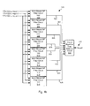
- FIG. 1b a detailed block diagram 100 of one implementation of data detector circuit 125 with multiple, multiple stream noise predictive filter circuits 502, 504, 506, 508, 510, 512, 514, 516, that each feed a respective one of branch metrics 522, 524, 526, 528, 530, 532, 534, 536 to a Viterbi algorithm data detector circuit 560.
- Viterbi algorithm data detector circuit 560 applies a data detection algorithm using the branch metrics 522, 524, 526, 528, 530, 532, 534, 536 to yield detected output 127. It should be noted that other implementations are possible in accordance with different embodiments of the present invention.
- Viterbi algorithm data detector circuit 560 may be replaced by another type of data detector circuit known in the art.
- Data detector circuit 125 includes, multiple stream noise predictive filter circuit 502 is designed to detect a '000' pattern, multiple stream noise predictive filter circuit 504 is designed to detect a '001' pattern, multiple stream noise predictive filter circuit 506 is designed to detect a '010' pattern, multiple stream noise predictive filter circuit 508 is designed to detect a '011' pattern, multiple stream noise predictive filter circuit 510 is designed to detect a '100' pattern, multiple stream noise predictive filter circuit 512 is designed to detect a '101' pattern, multiple stream noise predictive filter circuit 514 is designed to detect a '110' pattern, and multiple stream noise predictive filter circuit 516 is designed to detect a '111' pattern.
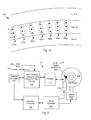
- a portion of a storage medium 600 is shown that includes three tracks (Track A, Track B, Track C).
- a read/write head (not shown) is flying above Track B taking samples, with the sample points 605 indicated as ellipses in dashed lines.
- the read/write head includes three sensors. At each sample point 605, the three sensors in the read/write head each sense information at a location indicated as A, B, C, respectively along Track B..
- the information sensed at positions A along Track B is provided as input 1 described above in relation to Fig. 1b ; the information sensed at positions B along Track B is provided as input 2 described above in relation to Fig. 1b ; and the information sensed at positions C along Track B is provided as input 3 described above in relation to Fig. 1b .
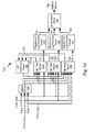
- Multi-stream noise predictive filter circuit 700 may be used in place of each of multi-stream noise predictive filters 502, 504, 506, 508, 510, 512, 514, 516 shown above in relation to Fig. 1b .
- multi-stream noise predictive filter circuit 700 includes a signal delay circuit 702 that delays each of input 1, input 2, and input 3 by a sample period to yield corresponding outputs input 1D, input 2D, input 3D. All of these delayed values are provided to a noise predictive filter circuit 710, a noise predictive filter circuit 730, and a noise predictive filter circuit 750.
- input 1 is provided to noise predictive filter circuit 710, noise predictive filter circuit 730 and noise predictive filter circuit 750;
- input 2 is provided to noise predictive filter circuit 730 and noise predictive filter circuit 750, and input 3 is provided to noise predictive filter circuit 750.
- Noise predictive filter circuit 710 applies noise predictive filtering to the received inputs to yield a filtered output 712.
- the noise predictive filtering yielding filtered output 712 is described by the following equation: p ⁇ e 0 , k
- y 0, k , y 1, k , y 2, k correspond to input 1, input 2, and input 3, respectively.
- ⁇ 0, k , ⁇ 1, k , ⁇ 2, k are the ideal outputs corresponding to y 0, k , y 1, k , y 2, k , respectively.
- These ideal outputs may be generated, for example, by convolving y 0, k , y 1, k , y 2, k with target values as is known in the art.
- the values of e 0, k , e 1, k , e 2, k correspond to error values for each of the respective input streams.
- the values of e 0, k -1 , e 1, k -1 , e 2, k -1 are the error values for the preceding instances of y 0, k , y 1, k , y 2, k (i.e., y 0, k -1 , y 1, k -1 , y 2, k -1 ), respectively.
- the values of f 0, j , f 1, j , and f 2, j are the filter coefficients for the noise predictive filters included in noise predictive filter circuit 710 applied to each of the respective inputs.
- ⁇ 0 is the variance of input 1.
- Noise predictive filter circuit 730 applies noise predictive filtering to the received inputs to yield a filtered output 732.
- the noise predictive filtering yielding filtered output 732 is described by the following equation: p ⁇ e 1 , k
- y 0, k , y 1, k , y 2, k correspond to input 1, input 2, and input 3, respectively.
- ⁇ 0, k , ⁇ 1, k , ⁇ 2, k are the ideal outputs corresponding to y 0, k , y 1, k , y 2, k , respectively.
- These ideal outputs may be generated, for example, by convolving y 0, k , y 1, k , y 2, k with target values as is known in the art.
- the values of e 0, k , e 1, k , e 2, k correspond to error values for each of the respective input streams.
- the values of e 0, k -1 , e 1, k -1 , e 2, k -1 are the error values for the preceding instances of y 0,k , y 1, k , y 2, k (i.e., y 0, k -1 , y 1, k -1 , y 2, k -1 ), respectively.
- the values of g 0, j , g 1, j , and g 2, j are the filter coefficients for the noise predictive filters included in noise predictive filter circuit 730 applied to each of the respective inputs.
- ⁇ 1 is the variance of input 2.
- Noise predictive filter circuit 750 applies noise predictive filtering to the received inputs to yield a filtered output 752.
- the noise predictive filtering yielding filtered output 752 is described by the following equation: p ⁇ e 2 , k
- y 0 ,k , y 1, k , y 2, k correspond to input 1, input 2, and input 3, respectively.
- ⁇ 0, k , ⁇ 1, k , ⁇ 2, k are the ideal outputs corresponding to y 0, k , y 1, k , y 2, k , respectively. These ideal outputs may be generated, for example, by convolving y 0, k , y 1, k , y 2, k with target values as is known in the art. As such, the values of e 0, k , e 1, k , e 2, k correspond to error values for each of the respective input streams.
- the values of e 0, k -1 , e 1 , k -1 , e 2, k -1 are the error values for the preceding instances of y 0, k , y 1, k , y 2, k (i.e., y 0, k -1 , y 1, k -1 , y 2, k -1 ), respectively.
- the values of ⁇ 0, j , ⁇ 1, j , and ⁇ 2, j are the filter coefficients for the noise predictive filters included in noise predictive filter circuit 730 applied to each of the respective inputs.
- ⁇ 2 is the variance of input 3.
- Filtered output 712 is provided to a square and log function circuit 720.
- Square and log function circuit 720 operates to square the Q 0 term to yield a processed output 722 as follows: p ⁇ e 0 , k
- filtered output 732 is provided to a square and log function circuit 740.
- Square and log function circuit 740 operates to square the Q 1 term and take a log of the overall p ⁇ e 1 , k
- filtered output 752 is provided to a square and log function circuit 760.
- Square and log function circuit 760 operates to square the Q 2 term and take a log of the overall p ⁇ e 2 , k
- Processed output 722, processed output 742 and processed output 762 are then summed using a summation circuit 780 to yield a branch metric output 790 that consists of three branch metrics, one corresponding to each of input 1, input 2, and input 3.
- a branch metric output 790 that consists of three branch metrics, one corresponding to each of input 1, input 2, and input 3.
- the resulting branch metric 790 is provided to Viterbi algorithm data detector circuit that traverses a trellis based upon the three branch metrics received as part of branch metric 790. It should be noted that the same process may be expanded to four or more inputs, or two inputs depending upon the particular application.
- Multi-stream noise predictive filter circuit 700 additionally includes a noise prediction calibration circuit 780.
- Noise prediction calibration circuit 780 operates to adaptively modify ⁇ 0 , j , ⁇ 1 , j , ⁇ 2 , j f 0 , j , f 1, j , f 2, j , g 0, j , g 1, j , and g 2, j in an attempt to reduce the value of e 0, k , e 1 ,k , e 2, k .
- the adaptive circuit is a least mean squared circuit.
- ⁇ 0, j , ⁇ 1, j ⁇ 2, j are provided to noise predictive filter circuit 750 as part of an output 782
- f 0, j , f 1, j , f 2, j are provided to noise predictive filter circuit 710 as part of output 782
- g 0, j , g 1, j , and g 2, j are provided to noise predictive filter circuit 730 as part of output 782.
- flow diagrams 200, 201 show a method in accordance with some embodiments of the present invention for data processing using multiple stream noise filtering.
- multiple analog inputs are received for a similar location along a track (block 205).
- three sensors are used that result in three analog inputs.
- Each of the analog inputs are converted to a respective series of digital samples (block 210). These conversions may be done using one or more analog to digital converter circuits as are known in the art. Of note, any circuit known in the art that is capable of converting an analog signal into a series of digital values representing the received analog signal may be used.
- the resulting series of digital samples are equalized to yield corresponding sets of equalized outputs (block 215).
- the equalization is done using one or more digital finite impulse response circuits as are known in the art. Based upon the disclosure provided herein, one of ordinary skill in the art will recognize a variety of equalizer circuits that may be used in place of such a digital finite impulse response circuit to perform equalization in accordance with different embodiments of the present invention.
- the equalized outputs are respectively buffered is buffered (block 220).
- a data detector circuit It is determined whether a data detector circuit is available (block 225). Where the data detector circuit is available (block 225), the next equalized outputs (i.e., the equalized outputs corresponding to the multiple analog inputs) from the sample buffer are selected for processing (block 230), and error values for the equalized outputs are calculated (block 231).
- e 0, k corresponds to a first of the analog inputs
- e 1, k corresponds to a second of the analog inputs
- e 2 , k corresponds to a third of the analog inputs
- y 0 ,k , y 1, k , y 2, k correspond to the three equalized outputs, respectively.
- ⁇ 0, k , ⁇ 1, k , ⁇ 2, k are the ideal outputs corresponding to y 0, k , y 1, k , y 2, k , respectively.
- These ideal outputs may be generated, for example, by convolving y 0, k , y 1, k , y 2, k with target values as is known in the art.
- Noise predictive filtering is applied to each of the equalized outputs in a process that interrelates all of the equalized outputs using adapted noise filter coefficients (i.e., ⁇ 0, j , ⁇ 1 , j, ⁇ 2,j f 0, j , f 1, j , f 2, j , g 0, j , g 1, j , and g 2, j ) to yield respective filtered outputs corresponding to each of the equalized outputs (block 233).
- adapted noise filter coefficients i.e., ⁇ 0, j , ⁇ 1 , j, ⁇ 2,j f 0, j , f 1, j , f 2, j , g 0, j , g 1, j , and g 2, j
- Noise predictive coefficients are adapted to reduce the error values (block 270), with the resulting coefficients ⁇ 0, j , ⁇ 1, j , ⁇ 2 ,j , f 0, j , f 1, j , f 2 ,j , g 0, j , g 1, j , and g 2, j used to perform the previously described noise predictive filtering (block 233).
- a square and log function is then applied to the filtered outputs to yield interim outputs (block 235).
- the square and log function operates to square the Q values in the above mentioned equations and taking a log of the overall equation leaving the following interim outputs:
- Interim Output 1 log ⁇ 1 2 ⁇ ⁇ ⁇ ⁇ 2 2 1 ⁇ 2 ⁇ 3 + Q 0 ;
- Interim Output 2 log ⁇ 1 2 ⁇ ⁇ ⁇ ⁇ 2 2 1 ⁇ 2 ⁇ 3 + Q 1 ;
- Interim Output 3 log ⁇ 1 2 ⁇ ⁇ ⁇ ⁇ 2 2 1 ⁇ 2 ⁇ 3 + Q 2
- the aforementioned interim outputs are then summed to yield a combined branch metric accounting for the interrelationship of the three analog inputs (block 237).
- the combined branch metric is then used to apply a data detection algorithm and make the most likely decision of the proper detected output corresponding to the three analog inputs (block 238). Where available, a prior decoded output corresponding to the combined branch metric is used to guide application of the data detection algorithm. The detected output is then stored to a central memory to await data decoding (block 240).
- the data decoder circuit may be, for example, a low density data decoder circuit as are known in the art. Where the data decoder circuit is available (block 206), a previously stored derivative of a detected output is accessed from the central memory and used as a received codeword (block 211). A data decode algorithm is applied to the received codeword to yield a decoded output (block 216). It is then determined whether the decoded output converged (e.g., resulted in the originally written data as indicated by the lack of remaining unsatisfied checks) (block 221). Where the decoded output converged (block 221), the converged codeword is provided as a decoded output (block 226).
- a decoded output e.g., resulted in the originally written data as indicated by the lack of remaining unsatisfied checks
- the decoded output failed to converge (e.g., errors remain) (block 221)
- the data decode algorithm is re-applied using the current decoded output as a guide (block 216).
- another local iteration is not desired (block 231)
- another global iteration is allowed where there is sufficient available space in the central memory and an output memory reordering queue to allow another pass through processing the currently processing codeword.
- the amount of available space in the central memory and an output memory reordering queue is a function of how many iterations are being used by concurrently processing codewords to converge.
- the output queue time limitation see, for example, US Pat. App. No. 12/114,462 entitled “Systems and Methods for Queue Based Data Detection and Decoding", and filed May 8, 2008 by Yang et al.
- the amount of time that a codeword may continue processing through global iterations is a function of the availability of central memory and an output memory reordering queue. By limiting the number of global iterations that may be performed, the amount of time a codeword may continue processing through global iterations can be reduced.
- a derivative of the decoded output is stored to the central memory (block 246).
- the derivative of the decoded output being stored to the central memory triggers the data set ready query of block 205 to begin the data detection process.
- a failure to converge is indicated (block 241), and the current decoded output is provided (block 226).
- Storage system 300 includes a read channel having multiple stream noise filtering circuitry in accordance with one or more embodiments of the present invention.
- Storage system 300 may be, for example, a hard disk drive.
- Storage system 300 also includes a preamplifier 370, an interface controller 320, a hard disk controller 366, a motor controller 368, a spindle motor 372, a disk platter 378, and a multi-reader read/write head assembly 376.
- Interface controller 320 controls addressing and timing of data to/from disk platter 378.
- the data on disk platter 378 consists of groups of magnetic signals that may be detected by read/write head assembly 376 when the assembly is properly positioned over disk platter 378.
- disk platter 378 includes magnetic signals recorded in accordance with either a longitudinal or a perpendicular recording scheme.
- multi-reader read/write head assembly 376 is accurately positioned by motor controller 368 over a desired data track on disk platter 378.
- Motor controller 368 both positions multi-reader read/write head assembly 376 in relation to disk platter 378 and drives spindle motor 372 by moving read/write head assembly to the proper data track on disk platter 378 under the direction of hard disk controller 366.
- Spindle motor 372 spins disk platter 378 at a determined spin rate (RPMs).
- RPMs spin rate
- the sensed magnetic signals are provided as multiple continuous, minute analog signals representative of the magnetic data on disk platter 378 at the locations corresponding to each of the respective readers. These minute analog signals are transferred from multi-reader read/write head assembly 376 to read channel circuit 310 via preamplifier 370. Preamplifier 370 is operable to amplify the minute analog signals accessed from disk platter 378. In turn, read channel circuit 310 decodes and digitizes the received analog signals to recreate the information originally written to disk platter 378. This data is provided as read data 303 to a receiving circuit. A write operation is substantially the opposite of the preceding read operation with write data 301 being provided to read channel circuit 310. This data is then encoded and written to disk platter 378.
- data is sensed from disk platter 378 at multiple locations at each sample point along a give track and processed through a data processing circuit including a data detector circuit and a data decoder circuit. Convergence on the originally written data set may involve one or more global iterations through both the data detector circuit and the data decoder circuit, and one or more local iterations through the data decoder circuit for each global iteration.
- the data detector circuit includes one or more multi-stream noise predictive filter circuits that combine the multiple streams into interdependent branch metrics. These branch metrics are used by the data detector circuit to establish a detected output. The detected output is then processed by the decoder circuit to derive the originally written data.
- data processing circuits similar to that discussed above in relation to Figs. 1a-1d may be used, and/or the processing may be done similar to that discussed above in relation to Figs. 2a-2b .
- storage system 300 may be integrated into a larger storage system such as, for example, a RAID (redundant array of inexpensive disks or redundant array of independent disks) based storage system.
- RAID redundant array of inexpensive disks or redundant array of independent disks
- Such a RAID storage system increases stability and reliability through redundancy, combining multiple disks as a logical unit.
- Data may be spread across a number of disks included in the RAID storage system according to a variety of algorithms and accessed by an operating system as if it were a single disk. For example, data may be mirrored to multiple disks in the RAID storage system, or may be sliced and distributed across multiple disks in a number of techniques.
- the disks in the RAID storage system may be, but are not limited to, individual storage systems such as storage system 300, and may be located in close proximity to each other or distributed more widely for increased security.
- write data is provided to a controller, which stores the write data across the disks, for example by mirroring or by striping the write data.
- the controller retrieves the data from the disks. The controller then yields the resulting read data as if the RAID storage system were a single disk.
- a data decoder circuit used in relation to read channel circuit 310 may be, but is not limited to, a low density parity check (LDPC) decoder circuit as are known in the art.
- LDPC low density parity check
- Transmission applications include, but are not limited to, optical fiber, radio frequency channels, wired or wireless local area networks, digital subscriber line technologies, wireless cellular, Ethernet over any medium such as copper or optical fiber, cable channels such as cable television, and Earth-satellite communications.
- Storage applications include, but are not limited to, hard disk drives, compact disks, digital video disks, magnetic tapes and memory devices such as DRAM, NAND flash, NOR flash, other non-volatile memories and solid state drives.
- storage system 300 may be modified to include solid state memory that is used to store data in addition to the storage offered by disk platter 378.
- This solid state memory may be used in parallel to disk platter 378 to provide additional storage.
- the solid state memory receives and provides information directly to read channel circuit 310.
- the solid state memory may be used as a cache where it offers faster access time than that offered by disk platted 378.
- the solid state memory may be disposed between interface controller 320 and read channel circuit 310 where it operates as a pass through to disk platter 378 when requested data is not available in the solid state memory or when the solid state memory does not have sufficient storage to hold a newly written data set. Based upon the disclosure provided herein, one of ordinary skill in the art will recognize a variety of storage systems including both disk platter 378 and a solid state memory.
- Such integrated circuits may include all of the functions of a given block, system or circuit, or only a subset of the block, system or circuit. Further, elements of the blocks, systems or circuits may be implemented across multiple integrated circuits. Such integrated circuits may be any type of integrated circuit known in the art including, but are not limited to, a monolithic integrated circuit, a flip chip integrated circuit, a multichip module integrated circuit, and/or a mixed signal integrated circuit. It should also be noted that various functions of the blocks, systems or circuits discussed herein may be implemented in either software or firmware. In some such cases, the entire system, block or circuit may be implemented using its software or firmware equivalent. In other cases, the one part of a given system, block or circuit may be implemented in software or firmware, while other parts are implemented in hardware.
Landscapes
- Engineering & Computer Science (AREA)
- Theoretical Computer Science (AREA)
- Physics & Mathematics (AREA)
- Probability & Statistics with Applications (AREA)
- Software Systems (AREA)
- General Engineering & Computer Science (AREA)
- General Physics & Mathematics (AREA)
- Signal Processing For Digital Recording And Reproducing (AREA)
- Error Detection And Correction (AREA)
Abstract
Description
- The present application claims priority to (is a non-provisional of)
US Pat. App. No. 61/871,437 - The present invention is related to systems and methods for branch metric calculation based on multiple data streams in a data processing circuit.
- Various data transfer systems have been developed including storage systems where data is transferred to and from a storage medium. The effectiveness of any transfer is impacted by noise arising in the data transfer, and the ability to accurately sense the data on the storage medium. To improve accuracy, multiple sensors may be used to sense the data on the storage medium. Each of the streams is processed and a result is derived. However, in some cases, the result derived from multiple streams is inaccurate do to an inability to adequately noise filter.
- Hence, for at least the aforementioned reasons, there exists a need in the art for advanced systems and methods for data processing.
- The present invention is related to systems and methods for branch metric calculation based on multiple data streams in a data processing circuit. According to a first aspect of the invention, there is provided a data processing system as set out in
claim 1. - Various embodiments of the present invention provide data processing systems that include: a first multi-stream noise predictive filter circuit operable to generate a first interim output corresponding to a first data input based upon a non-matrix based combination of the first data input and a previous instance of a second data input; a second multi-stream noise predictive filter circuit operable to generate a second interim output corresponding to the second data input based upon a non-matrix based combination of the second data input and a previous instance of the first data input; and a combining circuit operable to combine at least the first interim output with the second interim output to yield a combination branch metric.
- In embodiments, the data processing system further comprises: a data detector circuit including the first multi-stream noise predictive filter circuit and the second multi-stream noise predictive filter circuit, and operable to provide a detected output corresponding to the first data input and the second data input based at least in part on the combination branch metric.
- In embodiments, the data processing system further comprises: a data decoder circuit operable to apply a data decode algorithm to the detected output to recover an original data set corresponding to the first data input and the second data input. In embodiments, the data decode algorithm is a low density parity check algorithm.
- In embodiments, the data detector circuit applies a Viterbi algorithm data detection.
- In embodiments, operation of the first multi-stream noise predictive filter circuit is based at least in part on a first coefficient set, wherein operation of the second multi-stream noise predictive filter circuit is based at least in part on a second coefficient set, and wherein the system further comprises: a calibration circuit operable to: generate the first coefficient set based upon a difference between the first data input and an ideal first data input, and generate the second coefficient set based upon a difference between the second data input and an ideal second data input.
- In embodiments, the combining circuit is a summation circuit operable to sum the first interim output with at least the second interim output to yield the combination branch metric. In embodiments, generating the first interim output is done using a first linear computation, and wherein generating the second interim output is done using a second linear computation.
- In embodiments, the data processing system is implemented as part of a storage device including: a storage medium having at least a first track and a second track; and wherein a combination of the first data input and the second data input are selected from a group consisting of: a first data input and a second data input derived from the first track; and a first data input derived from the first track and the second data input derived from the second track. Additionally or alternatively, the data processing system is implemented as part of a storage device including a storage medium having tracks, wherein the first data input corresponds to a first sample location along a particular one of the tracks, wherein the second data input corresponds to a second sample location along the particular one of the tracks, and wherein the first sample location and the second sample location are sampled at the same sample time.
- In embodiments, the data processing system is implemented as part of an integrated circuit.
- In a related aspect of the invention, there is provided a method, the method comprising: generating a first interim output corresponding to a first data input using a first multi-stream noise predictive filter circuit based upon a non-matrix based combination of the first data input and a previous instance of a second data input; generating a second interim output corresponding to a second data input using a second multi-stream noise predictive filter circuit based upon a non-matrix based combination of the first data input and a previous instance of a second data input; and summing the first interim output with at least the second interim output to yield a combination branch metric.
- In embodiments, the method further comprises: applying a data detection algorithm relying on the combination branch metric to yield a detected output.
- In a related aspect of the invention there is provided a storage device, the storage device comprising: a storage medium; a head assembly disposed in relation to the storage medium and operable to provide a first sensed signal and a second sensed signal corresponding to information along a track of the storage medium; a read channel circuit including: an analog front end circuit operable to provide a first analog signal corresponding to the first sensed signal, and a second analog signal corresponding to the second sensed signal; an analog to digital converter circuit operable to sample the first analog signal to yield a first series of digital samples, and sample the second analog signal to yield a second series of digital samples; an equalizer circuit operable to equalize the first series of digital samples to yield a first sample set, and equalize the second series of digital samples to yield a second sample set; a data detector circuit including: a first multi-stream noise predictive filter circuit operable to generate a first interim output corresponding to the first sample set based upon a non-matrix based combination of the first sample set and corresponding previous instances of the second sample set; a second multi-stream noise predictive filter circuit operable to generate a second interim output corresponding to the second sample set based upon a non-matrix based combination of the first sample set and corresponding previous instances of the second sample set; a combining circuit operable to combine at least the first interim output with the second interim output to yield a combination branch metric; and operable to provide a detected output corresponding to the first data input and the second data input based at least in part on the combination branch metric.
- In embodiments, the read channel circuit further comprises: a data decoder circuit operable to apply a data decode algorithm to the detected output to recover an original data set corresponding to the first sample set and the second sample set.
- In embodiments, the data decode algorithm is a low density parity check algorithm. In embodiments, the data detector circuit applies a Viterbi algorithm data detection.
- In embodiments, operation of the first multi-stream noise predictive filter circuit is based at least in part on a first coefficient set, wherein operation of the second multi-stream noise predictive filter circuit is based at least in part on a second coefficient set, and wherein the system further comprises: a calibration circuit operable to: generate the first coefficient set based upon a difference between the first sample set and corresponding instances of an ideal first sample set, and generate the second coefficient set based upon a difference between the first sample set and corresponding instances of an ideal first sample set.
- In embodiments, generating the first interim output is done using a first linear computation, and wherein generating the second interim output is done using a second linear computation. In embodiments, the combining circuit is a summation circuit operable to sum the first interim output with at least the second interim output to yield the combination branch metric.
- This summary provides only a general outline of some embodiments of the invention. Many other objects, features, advantages and other embodiments of the invention will become more fully apparent from the following detailed description, the appended claims and the accompanying drawings.
- A further understanding of the various embodiments of the present invention may be realized by reference to the figures which are described in remaining portions of the specification. In the figures, like reference numerals are used throughout several figures to refer to similar components. In some instances, a sub-label consisting of a lower case letter is associated with a reference numeral to denote one of multiple similar components. When reference is made to a reference numeral without specification to an existing sub-label, it is intended to refer to all such multiple similar components.
-
Fig. 1a-1d depicts a data processing circuit having multiple stream noise filtering circuitry in accordance with some embodiments of the present invention; -
Figs. 2a-2b are flow diagrams showing a method in accordance with some embodiments of the present invention for data processing using multiple stream noise filtering; and -
Fig. 3 shows a storage device including a read channel having multiple stream noise filtering circuitry in accordance with one or more embodiments of the present invention. - The present invention is related to systems and methods for performing data processing, and more specifically to systems and methods for adaptive parameter modification in a data processing system.
- Various embodiments of the present invention provide data processing circuits that include a data detector circuit and a data decoder circuit. The data detector circuit includes one or more multiple stream noise prediction circuits as part of the data detector circuit. A detected output from the data detector circuit is provided to the data decoder circuit that applies a data decode algorithm in an attempt to recover an originally written data set. Where application of the data decode algorithm yields the originally written data set, the decoded output is said to have "converged". In some cases, such convergence is indicated by satisfaction of all parity check equations relied upon in the data decode algorithm. Based upon the disclosure provided herein, one of ordinary skill in the art will recognize a variety of scenarios in which the decoded output is considered to have converged. Such a converged data set is provided as an output from the data processing circuit. A pass through both the data detector circuit and the data decoder circuit is referred to herein as a "global iteration". In some cases, the data processing circuit is designed to allow multiple global iterations. In various cases, the data decoding circuit may apply the data decode algorithm to the detected output multiple times during a given global iteration. In such cases, each application of the data decode algorithm is referred to herein as a "local iteration".
- Various embodiments of the present invention provide data processing systems that include: a first multi-stream noise predictive filter circuit operable to generate a first interim output corresponding to a first data input based upon a non-matrix based combination of the first data input and a previous instance of a second data input; a second multi-stream noise predictive filter circuit operable to generate a second interim output corresponding to the second data input based upon a non-matrix based combination of the second data input and a previous instance of the first data input; and a combining circuit operable to combine at least the first interim output with the second interim output to yield a combination branch metric.
- In some instances of the aforementioned embodiments, the systems further include a data detector circuit including the first multi-stream noise predictive filter circuit and the second multi-stream noise predictive filter circuit, and operable to provide a detected output corresponding to the first data input and the second data input based at least in part on the combination branch metric. In some cases, the system further includes a data decoder circuit operable to apply a data decode algorithm to the detected output to recover an original data set corresponding to the first data input and the second data input. In one particular case, the data decode algorithm is a low density parity check algorithm. In some cases, the data detector circuit applies a Viterbi algorithm data detection.
- In one or more instances of the aforementioned embodiments, operation of the first multi-stream noise predictive filter circuit is based at least in part on a first coefficient set, and operation of the second multi-stream noise predictive filter circuit is based at least in part on a second coefficient set. In such instances, the systems further include a calibration circuit operable to: generate the first coefficient set based upon a difference between the first data input and an ideal first data input, and generate the second coefficient set based upon a difference between the second data input and an ideal second data input. In various instances of the aforementioned embodiment, the combining circuit is a summation circuit operable to sum the first interim output with at least the second interim output to yield the combination branch metric. In some instances of the aforementioned embodiments, generating the first interim output is done using a first linear computation, and generating the second interim output is done using a second linear computation.
- In various instances of the aforementioned embodiments, the data processing system is implemented as part of a storage device including a storage medium. The storage medium includes at least a first track and a second track. A combination of the first data input and the second data input may be a first data input and a second data input derived from the first track, or a first data input derived from the first track and the second data input derived from the second track where the branch metric label involves bit combinations from multiple tracks for joint detection. In some instances of the aforementioned embodiments, the data processing system is implemented as part of a storage device including a storage medium. The storage medium includes tracks. The first data input corresponds to a first sample location along a particular one of the tracks, the second data input corresponds to a second sample location along the particular one of the tracks, and the first sample location and the second sample location are sampled at the same sample time.
- Other embodiments of the present invention provide methods that include: generating a first interim output corresponding to a first data input using a first multi-stream noise predictive filter circuit based upon a non-matrix based combination of the first data input and a previous instance of a second data input; generating a second interim output corresponding to a second data input using a second multi-stream noise predictive filter circuit based upon a non-matrix based combination of the first data input and a previous instance of a second data input; and summing the first interim output with at least the second interim output to yield a combination branch metric.
- Yet other embodiments of the present invention provide storage devices that include: a storage medium; a head assembly disposed in relation to the storage medium and operable to provide a first sensed signal and a second sensed signal corresponding to information along a track of the storage medium; and a read channel circuit. The read channel circuit includes: an analog front end circuit operable to provide a first analog signal corresponding to the first sensed signal, and a second analog signal corresponding to the second sensed signal; an analog to digital converter circuit operable to sample the first analog signal to yield a first series of digital samples, and sample the second analog signal to yield a second series of digital samples; an equalizer circuit operable to equalize the first series of digital samples to yield a first sample set, and equalize the second series of digital samples to yield a second sample set; and a data detector circuit. The data detector circuit includes: a first multi-stream noise predictive filter circuit operable to generate a first interim output corresponding to the first sample set based upon a non-matrix based combination of the first sample set and corresponding previous instances of the second sample set; a second multi-stream noise predictive filter circuit operable to generate a second interim output corresponding to the second sample set based upon a non-matrix based combination of the first sample set and corresponding previous instances of the second sample set; a combining circuit operable to combine at least the first interim output with the second interim output to yield a combination branch metric; and the data detector circuit is operable to provide a detected output corresponding to the first data input and the second data input based at least in part on the combination branch metric.
- Turning to
Fig. 1a , adata processing circuit 100 having adata detector circuit 125 with multiple stream noise predictive filter circuits is shown in accordance with some embodiments of the present invention.Data processing circuit 100 includes an analogfront end circuit 110 that receives three different analog inputs (i.e.,analog input 108a,analog input 108b,analog input 108c). Analogfront end circuit 110 processes each ofanalog input 108a,analog input 108b, andanalog input 108c to yield respective processed analog signals (i.e., processedanalog signal 112a, processedanalog signal 112b, processedanalog signal 112c) which are provided to an analog todigital converter circuit 115. Analogfront end circuit 110 may include, but is not limited to, three parallel analog filters and three parallel amplifier circuits as are known in the art. Based upon the disclosure provided herein, one of ordinary skill in the art will recognize a variety of circuitry that may be included as part of analogfront end circuit 110. In some cases,analog input 108a is derived from a first sensor of a read/write head assembly (not shown),analog input 108b is derived from a second sensor of the read/write head assembly, and theanalog input 108c is derived from a third sensor of the read/write head assembly. The read/write head assembly is disposed in relation to a storage medium (not shown). - Analog to
digital converter circuit 115 converts processedanalog signal 112a into a first series ofdigital samples 117a, processedanalog signal 112b into a second series ofdigital samples 117b, and processedanalog signal 112c into a third series ofdigital samples 117c. Analog todigital converter circuit 115 may be any circuit known in the art that is capable of producing digital samples corresponding to an analog input signal. In one particular embodiment of the present invention, analog todigital converter circuit 115 has three parallel converter circuits each processing a respective one ofdigital samples 117a,digital samples 117b, anddigital samples 117c. Based upon the disclosure provided herein, one of ordinary skill in the art will recognize a variety of analog to digital converter circuits that may be used in relation to different embodiments of the present invention.Digital samples 117a,digital samples 117b, anddigital samples 117c are provided to anequalizer circuit 120.Equalizer circuit 120 applies an equalization algorithm to the respectivedigital samples 117a,digital samples 117b, anddigital samples 117c to yield respective equalizedoutput 122a, equalizedoutput 122b, and equalizedoutput 122c. In some embodiments of the present invention,equalizer circuit 120 is a digital finite impulse response filter circuit as are known in the art. In one particular case,equalizer circuit 120 includes three finite impulse response filter circuits in parallel to process respective ones ofdigital samples 117a,digital samples 117b, anddigital samples 117c. - Equalized
output 122a, equalizedoutput 122b, equalizedoutput 122c are provided to bothdata detector circuit 125 and to asample buffer circuit 175. In some casesdata detector circuit 125 includes a primary data detector circuit and a secondary data detector circuit. In such a case, the equalizedoutputs buffer circuit 175.Sample buffer circuit 175 stores the equalizedoutputs data 177a, buffereddata 177b, buffereddata 177c, respectively, for use in subsequent iterations throughdata detector circuit 125.Data detector circuit 125 may be any data detector circuit known in the art that is capable of producing a detectedoutput 127 from the three data streams. As some examples,data detector circuit 125 may be, but is not limited to, a Viterbi algorithm detector circuit or a maximum a posteriori detector circuit as are known in the art. Of note, the general phrases "Viterbi data detection algorithm" or "Viterbi algorithm data detector circuit" are used in their broadest sense to mean any Viterbi detection algorithm or Viterbi algorithm detector circuit or variations thereof including, but not limited to, bi-direction Viterbi detection algorithm or bi-direction Viterbi algorithm detector circuit. Also, the general phrases "maximum a posteriori data detection algorithm" or "maximum a posteriori data detector circuit" are used in their broadest sense to mean any maximum a posteriori detection algorithm or detector circuit or variations thereof including, but not limited to, simplified maximum a posteriori data detection algorithm and a max-log maximum a posteriori data detection algorithm, or corresponding detector circuits. Based upon the disclosure provided herein, one of ordinary skill in the art will recognize a variety of data detector circuits that may be used in relation to different embodiments of the present invention. Detectedoutput 127 may include both hard decisions and soft decisions. The terms "hard decisions" and "soft decisions" are used in their broadest sense. In particular, "hard decisions" are outputs indicating an expected original input value (e.g., a binary '1' or '0', or a non-binary digital value), and the "soft decisions" indicate a likelihood that corresponding hard decisions are correct. Based upon the disclosure provided herein, one of ordinary skill in the art will recognize a variety of hard decisions and soft decisions that may be used in relation to different embodiments of the present invention. - Detected
output 127 is provided to a centralqueue memory circuit 160 that operates to buffer data passed betweendata detector circuit 125 anddata decoder circuit 150. In some cases, centralqueue memory circuit 160 includes interleaving (i.e., data shuffling) and deinterleaving (i.e., data un-shuffling) circuitry known in the art. Whendata decoder circuit 150 is available,data decoder circuit 150 accesses detectedoutput 127 from centralqueue memory circuit 160 as adecoder input 156.Data decoder circuit 150 applies a data decoding algorithm todecoder input 156 in an attempt to recover originally written data. The result of the data decoding algorithm is provided as a decodedoutput 152. Similar to detectedoutput 127, decodedoutput 152 may include both hard decisions and soft decisions. For example,data decoder circuit 150 may be any data decoder circuit known in the art that is capable of applying a decoding algorithm to a received input.Data decoder circuit 150 may be, but is not limited to, a low density parity check (LDPC) decoder circuit or a Reed Solomon decoder circuit as are known in the art. Based upon the disclosure provided herein, one of ordinary skill in the art will recognize a variety of data decoder circuits that may be used in relation to different embodiments of the present invention. Where the original data is recovered (i.e., the data decoding algorithm converges) or a timeout condition occurs (e.g., ifsample buffer circuit 175 is close to getting filled up), decodedoutput 152 is stored to a memory included in a harddecision output circuit 180. In turn, harddecision output circuit 180 provides the converged decodedoutput 152 as adata output 184 to a recipient (not shown). The recipient may be, for example, an interface circuit operable to receive processed data sets. Based upon the disclosure provided herein, one of ordinary skill in the art will recognize a variety of recipients that may be used in relation to different embodiments of the present invention. Where the original data is not recovered (i.e., the data decoding algorithm failed to converge) prior to a timeout condition, decodedoutput 152 indicates that the data is unusable as is more specifically discussed below, anddata output 184 is similarly identified as unusable. - One or more iterations through the combination of
data detector circuit 125 anddata decoder circuit 150 may be made in an effort to converge on the originally written data set. As mentioned above, processing through both the data detector circuit and the data decoder circuit is referred to as a "global iteration". For the first global iteration,data detector circuit 125 applies the data detection algorithm to equalizedoutputs data detector circuit 125 applies the data detection algorithm to buffereddata output 152. To facilitate this guidance, decodedoutput 152 is stored to centralqueue memory circuit 160 as adecoder output 154, and is provided from centralqueue memory circuit 160 as adetector input 129 when equalizedoutputs data detector circuit 125. - During each global iteration it is possible for
data decoder circuit 150 to make one or more local iterations including application of the data decoding algorithm todecoder input 156. For the first local iteration,data decoder circuit 150 applies the data decoder algorithm without guidance from decodedoutput 152. For subsequent local iterations,data decoder circuit 150 applies the data decoding algorithm todecoder input 156 as guided by a previousdecoded output 152. The number of local iterations allowed may be, for example, ten. Based upon the disclosure provided herein, one of ordinary skill in the art will recognize a variety of different numbers of local iterations that may be allowed in accordance with different embodiments of the present invention. Where the number of local iterations throughdata decoder circuit 150 exceeds that allowed, but it is determined that at least one additional global iteration during standard processing of the data set is allowed, decodedoutput 152 is provided back to centralqueue memory circuit 160 as decodedoutput 154.Decoded output 154 is maintained in centralqueue memory circuit 160 untildata detector circuit 125 becomes available to perform additional processing. - In contrast, where the number of local iterations through
data decoder circuit 150 exceeds that allowed and it is determined that the allowable number of global iterations has been surpassed for the data set and/or a timeout or memory usage calls for termination of processing of the particular data set, standard processing of the data set concludes and an error is indicated. In some cases, retry processing or some offline processing may be applied to recover the otherwise unconverged data set. Based upon the disclosure provided herein, one of ordinary skill in the art will recognize a variety of non-standard processing techniques that may be applied to recover the otherwise unrecoverable data set. - Turning to
Fig. 1b , a detailed block diagram 100 of one implementation ofdata detector circuit 125 with multiple, multiple stream noisepredictive filter circuits branch metrics data detector circuit 560. Viterbi algorithmdata detector circuit 560 applies a data detection algorithm using thebranch metrics output 127. It should be noted that other implementations are possible in accordance with different embodiments of the present invention. In addition, it should be noted that Viterbi algorithmdata detector circuit 560 may be replaced by another type of data detector circuit known in the art.Data detector circuit 125 includes, multiple stream noisepredictive filter circuit 502 is designed to detect a '000' pattern, multiple stream noisepredictive filter circuit 504 is designed to detect a '001' pattern, multiple stream noisepredictive filter circuit 506 is designed to detect a '010' pattern, multiple stream noisepredictive filter circuit 508 is designed to detect a '011' pattern, multiple stream noisepredictive filter circuit 510 is designed to detect a '100' pattern, multiple stream noisepredictive filter circuit 512 is designed to detect a '101' pattern, multiple stream noisepredictive filter circuit 514 is designed to detect a '110' pattern, and multiple stream noise predictive filter circuit 516 is designed to detect a '111' pattern. Aninput 1 corresponds to buffereddata 177a or equalizedoutputs 122a depending upon whether it is a first or later global iteration; aninput 2 corresponds to buffereddata 177b or equalizedoutputs 122b depending upon whether it is a first or later global iteration; and aninput 3 corresponds to buffereddata 177c or equalizedoutputs 122c depending upon whether it is a first or later global iteration. - Turning to
Fig. 1c , a portion of astorage medium 600 is shown that includes three tracks (Track A, Track B, Track C). A read/write head (not shown) is flying above Track B taking samples, with the sample points 605 indicated as ellipses in dashed lines. The read/write head includes three sensors. At each sample point 605, the three sensors in the read/write head each sense information at a location indicated as A, B, C, respectively along Track B.. The information sensed at positions A along Track B is provided asinput 1 described above in relation toFig. 1b ; the information sensed at positions B along Track B is provided asinput 2 described above in relation toFig. 1b ; and the information sensed at positions C along Track B is provided asinput 3 described above in relation toFig. 1b . - Turning to
Fig. 1d , an implementation of a multi-stream noisepredictive filter circuit 700 is shown in accordance with one or more embodiments of the present invention. Multi-stream noisepredictive filter circuit 700 may be used in place of each of multi-stream noisepredictive filters Fig. 1b . As shown, multi-stream noisepredictive filter circuit 700 includes asignal delay circuit 702 that delays each ofinput 1,input 2, andinput 3 by a sample period to yield corresponding outputs input 1D, input 2D, input 3D. All of these delayed values are provided to a noisepredictive filter circuit 710, a noisepredictive filter circuit 730, and a noisepredictive filter circuit 750. In addition,input 1 is provided to noisepredictive filter circuit 710, noisepredictive filter circuit 730 and noisepredictive filter circuit 750;input 2 is provided to noisepredictive filter circuit 730 and noisepredictive filter circuit 750, andinput 3 is provided to noisepredictive filter circuit 750. - Noise
predictive filter circuit 710 applies noise predictive filtering to the received inputs to yield afiltered output 712. The noise predictive filtering yieldingfiltered output 712 is described by the following equation:


input 2, andinput 3, respectively. ŷ 0,k , ŷ 1,k , ŷ 2,k are the ideal outputs corresponding to y 0,k , y 1,k , y 2,k , respectively. These ideal outputs may be generated, for example, by convolving y 0,k , y 1,k , y 2,k with target values as is known in the art. As such, the values of e 0,k , e 1,k , e 2,k correspond to error values for each of the respective input streams. Additionally, the values of e 0,k-1, e 1,k-1, e 2,k-1 are the error values for the preceding instances of y 0,k , y 1,k , y 2,k (i.e., y 0,k-1, y 1,k-1, y 2,k-1), respectively. The values of f 0,j , f 1,j , and f 2,j are the filter coefficients for the noise predictive filters included in noisepredictive filter circuit 710 applied to each of the respective inputs. σ0 is the variance ofinput 1. - Noise
predictive filter circuit 730 applies noise predictive filtering to the received inputs to yield afiltered output 732. The noise predictive filtering yieldingfiltered output 732 is described by the following equation:


input 2, andinput 3, respectively. ŷ 0,k , ŷ 1,k , ŷ 2,k are the ideal outputs corresponding to y 0,k , y 1,k , y 2,k , respectively. These ideal outputs may be generated, for example, by convolving y 0, k, y 1,k , y 2,k with target values as is known in the art. As such, the values of e 0, k, e 1,k , e 2,k correspond to error values for each of the respective input streams. Additionally, the values of e 0,k-1, e 1,k-1, e 2,k-1 are the error values for the preceding instances of y0,k, y 1,k , y 2,k (i.e., y 0,k-1, y 1,k-1, y 2,k-1), respectively. The values of g 0,j , g 1,j , and g 2,j are the filter coefficients for the noise predictive filters included in noisepredictive filter circuit 730 applied to each of the respective inputs. σ1 is the variance ofinput 2. - Noise
predictive filter circuit 750 applies noise predictive filtering to the received inputs to yield afiltered output 752. The noise predictive filtering yieldingfiltered output 752 is described by the following equation:

- Again, the following equations define the values e 0,k , e 1,k , e 2,k :


input 2, andinput 3, respectively. ŷ 0,k , ŷ 1,k , ŷ 2,k are the ideal outputs corresponding to y 0,k , y 1,k , y 2,k , respectively. These ideal outputs may be generated, for example, by convolving y 0,k , y 1,k , y 2,k with target values as is known in the art. As such, the values of e 0, k, e 1,k , e 2,k correspond to error values for each of the respective input streams. Additionally, the values of e 0,k-1, e 1,k-1, e 2,k-1 are the error values for the preceding instances of y 0,k , y 1,k , y 2,k (i.e., y 0,k-1, y 1,k-1, y 2,k-1), respectively. The values of η0,j , η1,j , and η 2,j are the filter coefficients for the noise predictive filters included in noisepredictive filter circuit 730 applied to each of the respective inputs. σ2 is the variance ofinput 3. - Filtered
output 712 is provided to a square andlog function circuit 720. Square and logfunction circuit 720 operates to square the Q 0 term to yield a processedoutput 722 as follows:

output 732 is provided to a square andlog function circuit 740. Square and logfunction circuit 740 operates to square the Q 1 term and take a log of the overall
output 742 as follows:
output 752 is provided to a square andlog function circuit 760. Square and logfunction circuit 760 operates to square the Q 2 term and take a log of the overall

-
Processed output 722, processedoutput 742 and processed output 762 are then summed using asummation circuit 780 to yield a branchmetric output 790 that consists of three branch metrics, one corresponding to each ofinput 1,input 2, andinput 3. Of note, the aforementioned process yields a branch metric based upon three different input streams that is more accurate than that achievable by averaging the three input streams, but less computational complex than doing it using matrix equations. The resultingbranch metric 790 is provided to Viterbi algorithm data detector circuit that traverses a trellis based upon the three branch metrics received as part ofbranch metric 790. It should be noted that the same process may be expanded to four or more inputs, or two inputs depending upon the particular application. - Multi-stream noise
predictive filter circuit 700 additionally includes a noiseprediction calibration circuit 780. Noiseprediction calibration circuit 780 operates to adaptively modify η0,j,η 1,j ,η 2, j f 0,j ,f 1,j ,f 2,j , g 0,j , g 1,j , and g 2,j in an attempt to reduce the value of e 0,k , e1 ,k, e 2, k. In some embodiments of the present invention, the adaptive circuit is a least mean squared circuit. Upon calculation, η 0,j ,η 1, jη 2,j are provided to noisepredictive filter circuit 750 as part of an output 782, f 0,j , f 1,j , f 2,j are provided to noisepredictive filter circuit 710 as part of output 782, and g 0,j , g 1,j , and g 2,j are provided to noisepredictive filter circuit 730 as part of output 782. - Turning to
Figs. 2a-2b , flow diagrams 200, 201 show a method in accordance with some embodiments of the present invention for data processing using multiple stream noise filtering. Following flow diagram 200 ofFig. 2a , multiple analog inputs are received for a similar location along a track (block 205). In one particular embodiment of the present invention, three sensors are used that result in three analog inputs. Each of the analog inputs are converted to a respective series of digital samples (block 210). These conversions may be done using one or more analog to digital converter circuits as are known in the art. Of note, any circuit known in the art that is capable of converting an analog signal into a series of digital values representing the received analog signal may be used. The resulting series of digital samples are equalized to yield corresponding sets of equalized outputs (block 215). In some embodiments of the present invention, the equalization is done using one or more digital finite impulse response circuits as are known in the art. Based upon the disclosure provided herein, one of ordinary skill in the art will recognize a variety of equalizer circuits that may be used in place of such a digital finite impulse response circuit to perform equalization in accordance with different embodiments of the present invention. The equalized outputs are respectively buffered is buffered (block 220). - It is determined whether a data detector circuit is available (block 225). Where the data detector circuit is available (block 225), the next equalized outputs (i.e., the equalized outputs corresponding to the multiple analog inputs) from the sample buffer are selected for processing (block 230), and error values for the equalized outputs are calculated (block 231). The error values are calculated in accordance with the following equations:


- Noise predictive filtering is applied to each of the equalized outputs in a process that interrelates all of the equalized outputs using adapted noise filter coefficients (i.e., η0,j, η 1, j, η2,j f 0,j , f 1,j , f 2,j , g 0,j , g 1,j , and g 2,j ) to yield respective filtered outputs corresponding to each of the equalized outputs (block 233). The following equations describe the filtered outputs resulting from each of the streams:


- A square and log function is then applied to the filtered outputs to yield interim outputs (block 235). The square and log function operates to square the Q values in the above mentioned equations and taking a log of the overall equation leaving the following interim outputs:


- The combined branch metric is then used to apply a data detection algorithm and make the most likely decision of the proper detected output corresponding to the three analog inputs (block 238). Where available, a prior decoded output corresponding to the combined branch metric is used to guide application of the data detection algorithm. The detected output is then stored to a central memory to await data decoding (block 240).
- Turning to
Fig. 2b and following flow diagram 201, in parallel to the previously described data detection process, it is determined whether a data decoder circuit is available (block 206). The data decoder circuit may be, for example, a low density data decoder circuit as are known in the art. Where the data decoder circuit is available (block 206), a previously stored derivative of a detected output is accessed from the central memory and used as a received codeword (block 211). A data decode algorithm is applied to the received codeword to yield a decoded output (block 216). It is then determined whether the decoded output converged (e.g., resulted in the originally written data as indicated by the lack of remaining unsatisfied checks) (block 221). Where the decoded output converged (block 221), the converged codeword is provided as a decoded output (block 226). - Alternatively, where the decoded output failed to converge (e.g., errors remain) (block 221), it is determined whether another local iteration is desired (block 231). In some cases, as a default seven local iterations are allowed per each global iteration. Based upon the disclosure provided herein, one of ordinary skill in the art will recognize another default number of local iterations that may be used in relation to different embodiments of the present invention. Where another local iteration is desired (block 231), the data decode algorithm is re-applied using the current decoded output as a guide (block 216).
- Alternatively, where another local iteration is not desired (block 231), it is determined whether another global iteration is allowed (block 236). As a default, another global iteration is allowed where there is sufficient available space in the central memory and an output memory reordering queue to allow another pass through processing the currently processing codeword. The amount of available space in the central memory and an output memory reordering queue is a function of how many iterations are being used by concurrently processing codewords to converge. For more detail on the output queue time limitation see, for example,
US Pat. App. No. 12/114,462 - Where another global iteration is allowed (block 236), a derivative of the decoded output is stored to the central memory (block 246). The derivative of the decoded output being stored to the central memory triggers the data set ready query of
block 205 to begin the data detection process. Alternatively, where another global iteration is not allowed (block 536), a failure to converge is indicated (block 241), and the current decoded output is provided (block 226). - Turning to
Fig. 3 , astorage device 300 is shown that includes a read channel having multiple stream noise filtering circuitry in accordance with one or more embodiments of the present invention.Storage system 300 may be, for example, a hard disk drive.Storage system 300 also includes apreamplifier 370, aninterface controller 320, a hard disk controller 366, a motor controller 368, aspindle motor 372, adisk platter 378, and a multi-reader read/write head assembly 376.Interface controller 320 controls addressing and timing of data to/fromdisk platter 378. The data ondisk platter 378 consists of groups of magnetic signals that may be detected by read/write head assembly 376 when the assembly is properly positioned overdisk platter 378. In one embodiment,disk platter 378 includes magnetic signals recorded in accordance with either a longitudinal or a perpendicular recording scheme. - In a typical read operation, multi-reader read/
write head assembly 376 is accurately positioned by motor controller 368 over a desired data track ondisk platter 378. Motor controller 368 both positions multi-reader read/write head assembly 376 in relation todisk platter 378 and drivesspindle motor 372 by moving read/write head assembly to the proper data track ondisk platter 378 under the direction of hard disk controller 366.Spindle motor 372 spinsdisk platter 378 at a determined spin rate (RPMs). Once multi-reader read/write head assembly 378 is positioned adjacent the proper data track, magnetic signals representing data ondisk platter 378 are sensed at locations corresponding to each of the readers in multi-reader read/write head assembly 376 asdisk platter 378 is rotated byspindle motor 372. The sensed magnetic signals are provided as multiple continuous, minute analog signals representative of the magnetic data ondisk platter 378 at the locations corresponding to each of the respective readers. These minute analog signals are transferred from multi-reader read/write head assembly 376 to readchannel circuit 310 viapreamplifier 370.Preamplifier 370 is operable to amplify the minute analog signals accessed fromdisk platter 378. In turn, readchannel circuit 310 decodes and digitizes the received analog signals to recreate the information originally written todisk platter 378. This data is provided as readdata 303 to a receiving circuit. A write operation is substantially the opposite of the preceding read operation withwrite data 301 being provided to readchannel circuit 310. This data is then encoded and written todisk platter 378. - During a read operation, data is sensed from
disk platter 378 at multiple locations at each sample point along a give track and processed through a data processing circuit including a data detector circuit and a data decoder circuit. Convergence on the originally written data set may involve one or more global iterations through both the data detector circuit and the data decoder circuit, and one or more local iterations through the data decoder circuit for each global iteration. The data detector circuit includes one or more multi-stream noise predictive filter circuits that combine the multiple streams into interdependent branch metrics. These branch metrics are used by the data detector circuit to establish a detected output. The detected output is then processed by the decoder circuit to derive the originally written data. In some embodiments of the present invention, data processing circuits similar to that discussed above in relation toFigs. 1a-1d may be used, and/or the processing may be done similar to that discussed above in relation toFigs. 2a-2b . - It should be noted that
storage system 300 may be integrated into a larger storage system such as, for example, a RAID (redundant array of inexpensive disks or redundant array of independent disks) based storage system. Such a RAID storage system increases stability and reliability through redundancy, combining multiple disks as a logical unit. Data may be spread across a number of disks included in the RAID storage system according to a variety of algorithms and accessed by an operating system as if it were a single disk. For example, data may be mirrored to multiple disks in the RAID storage system, or may be sliced and distributed across multiple disks in a number of techniques. If a small number of disks in the RAID storage system fail or become unavailable, error correction techniques may be used to recreate the missing data based on the remaining portions of the data from the other disks in the RAID storage system. The disks in the RAID storage system may be, but are not limited to, individual storage systems such asstorage system 300, and may be located in close proximity to each other or distributed more widely for increased security. In a write operation, write data is provided to a controller, which stores the write data across the disks, for example by mirroring or by striping the write data. In a read operation, the controller retrieves the data from the disks. The controller then yields the resulting read data as if the RAID storage system were a single disk. - A data decoder circuit used in relation to read
channel circuit 310 may be, but is not limited to, a low density parity check (LDPC) decoder circuit as are known in the art. Such low density parity check technology is applicable to transmission of information over virtually any channel or storage of information on virtually any media. Transmission applications include, but are not limited to, optical fiber, radio frequency channels, wired or wireless local area networks, digital subscriber line technologies, wireless cellular, Ethernet over any medium such as copper or optical fiber, cable channels such as cable television, and Earth-satellite communications. Storage applications include, but are not limited to, hard disk drives, compact disks, digital video disks, magnetic tapes and memory devices such as DRAM, NAND flash, NOR flash, other non-volatile memories and solid state drives. - In addition, it should be noted that
storage system 300 may be modified to include solid state memory that is used to store data in addition to the storage offered bydisk platter 378. This solid state memory may be used in parallel todisk platter 378 to provide additional storage. In such a case, the solid state memory receives and provides information directly to readchannel circuit 310. Alternatively, the solid state memory may be used as a cache where it offers faster access time than that offered by disk platted 378. In such a case, the solid state memory may be disposed betweeninterface controller 320 and readchannel circuit 310 where it operates as a pass through todisk platter 378 when requested data is not available in the solid state memory or when the solid state memory does not have sufficient storage to hold a newly written data set. Based upon the disclosure provided herein, one of ordinary skill in the art will recognize a variety of storage systems including bothdisk platter 378 and a solid state memory. - It should be noted that the various blocks discussed in the above application may be implemented in integrated circuits along with other functionality. Such integrated circuits may include all of the functions of a given block, system or circuit, or only a subset of the block, system or circuit. Further, elements of the blocks, systems or circuits may be implemented across multiple integrated circuits. Such integrated circuits may be any type of integrated circuit known in the art including, but are not limited to, a monolithic integrated circuit, a flip chip integrated circuit, a multichip module integrated circuit, and/or a mixed signal integrated circuit. It should also be noted that various functions of the blocks, systems or circuits discussed herein may be implemented in either software or firmware. In some such cases, the entire system, block or circuit may be implemented using its software or firmware equivalent. In other cases, the one part of a given system, block or circuit may be implemented in software or firmware, while other parts are implemented in hardware.
- In conclusion, the invention provides novel systems, devices, methods and arrangements for data processing. While detailed descriptions of one or more embodiments of the invention have been given above, various alternatives, modifications, and equivalents will be apparent to those skilled in the art. Therefore, the above description should not be taken as limiting the scope of the invention, which is defined by the appended claims.
Claims (15)
- A data processing system, the data processing system (100) comprising:a first multi-stream noise predictive filter circuit operable to generate a first interim output corresponding to a first data input based upon a non-matrix based combination of the first data input and a previous instance of a second data input;a second multi-stream noise predictive filter circuit operable to generate a second interim output corresponding to the second data input based upon a non-matrix based combination of the second data input and a previous instance of the first data input; anda combining circuit operable to combine at least the first interim output with the second interim output to yield a combination branch metric.
- The data processing system of claim 1, the system further comprises:a data detector circuit (125) including the first multi-stream noise predictive filter circuit and the second multi-stream noise predictive filter circuit, and operable to provide a detected output (127) corresponding to the first data input and the second data input based at least in part on the combination branch metric.
- The data processing system of claim 2, the system further comprising:a data decoder circuit (150) operable to apply a data decode algorithm to the detected output (127) to recover an original data set corresponding to the first data input and the second data inputpreferably wherein the data decode algorithm is a low density parity check algorithm.
- The data processing system of claim 2, wherein the data detector circuit (125) applies a Viterbi algorithm data detection.
- The data processing system of any one of the preceding claims, wherein operation of the first multi-stream noise predictive filter circuit is based at least in part on a first coefficient set, wherein operation of the second multi-stream noise predictive filter circuit is based at least in part on a second coefficient set, and wherein the system further comprises:a calibration circuit (780) operable to:generate the first coefficient set based upon a difference between the first data input and an ideal first data input, andgenerate the second coefficient set based upon a difference between the second data input and an ideal second data input.
- The data processing system of any one of the preceding claims, wherein:the combining circuit is a summation circuit (780) operable to sum the first interim output with at least the second interim output to yield the combination branch metric; and/orgenerating the first interim output is done using a first linear computation, and wherein generating the second interim output is done using a second linear computation.
- The data processing system of any one of the preceding claims, wherein the data processing system is implemented as part of a storage device (300) including:a storage medium having at least a first track and a second track; and wherein a combination of the first data input and the second data input are selected from a group consisting of: a first data input and a second data input derived from the first track; and a first data input derived from the first track and the second data input derived from the second track; ora storage medium having tracks, wherein the first data input corresponds to a first sample location along a particular one of the tracks, wherein the second data input corresponds to a second sample location along the particular one of the tracks, and wherein the first sample location and the second sample location are sampled at the same sample time.
- The data processing system of any one of the preceding claims, wherein the data processing system is implemented as part of an integrated circuit.
- A method, the method comprising:generating a first interim output corresponding to a first data input using a first multi-stream noise predictive filter circuit based upon a non-matrix based combination of the first data input and a previous instance of a second data input;generating a second interim output corresponding to a second data input using a second multi-stream noise predictive filter circuit based upon a non-matrix based combination of the first data input and a previous instance of a second data input; andsumming the first interim output with at least the second interim output to yield a combination branch metric.
- The method of claim 9, wherein the method further comprises: applying a data detection algorithm relying on the combination branch metric to yield a detected output (127).
- A storage device (300), the storage device comprising:a storage medium;a head assembly (376) disposed in relation to the storage medium and operable to provide a first sensed signal and a second sensed signal corresponding to information along a track of the storage medium;a read channel circuit (310) including:an analog front end circuit (110) operable to provide a first analog signal corresponding to the first sensed signal, and a second analog signal corresponding to the second sensed signal;an analog to digital converter circuit (115) operable to sample the first analog signal (112a) to yield a first series of digital samples (117a), and sample the second analog signal (112b) to yield a second series of digital samples (117b);an equalizer circuit (120) operable to equalize the first series of digital samples (117a) to yield a first sample set (122a), and equalize the second series of digital samples (117b) to yield a second sample set (122b);a data detector circuit (125) including:a first multi-stream noise predictive filter circuit operable to generate a first interim output corresponding to the first sample set based upon a non-matrix based combination of the first sample set and corresponding previous instances of the second sample set;a second multi-stream noise predictive filter circuit operable to generate a second interim output corresponding to the second sample set based upon a non-matrix based combination of the first sample set and corresponding previous instances of the second sample set;a combining circuit operable to combine at least the first interim output with the second interim output to yield a combination branch metric; andoperable to provide a detected output corresponding to the first data input and the second data input based at least in part on the combination branch metric.
- The storage device of claim 11, wherein the read channel circuit (310) further comprises:a data decoder circuit (150) operable to apply a data decode algorithm to the detected output (127) to recover an original data set corresponding to the first sample set and the second sample set.
- The storage device of claim 12, wherein:the data decode algorithm is a low density parity check algorithm; and/orthe data detector circuit applies a Viterbi algorithm data detection.
- The storage device of any one of claims 11 to 13, wherein operation of the first multi-stream noise predictive filter circuit is based at least in part on a first coefficient set, wherein operation of the second multi-stream noise predictive filter circuit is based at least in part on a second coefficient set, and wherein the system further comprises:a calibration circuit (780) operable to:generate the first coefficient set based upon a difference between the first sample set and corresponding instances of an ideal first sample set, andgenerate the second coefficient set based upon a difference between the first sample set and corresponding instances of an ideal first sample set.
- The storage device of any one of claims 11 to 14, wherein:generating the first interim output is done using a first linear computation, and wherein generating the second interim output is done using a second linear computation; and/orthe combining circuit is a summation circuit operable to sum the first interim output with at least the second interim output to yield the combination branch metric.
Applications Claiming Priority (2)
| Application Number | Priority Date | Filing Date | Title |
|---|---|---|---|
| US201361871437P | 2013-08-29 | 2013-08-29 | |
| US14/025,409 US9430270B2 (en) | 2013-08-29 | 2013-09-12 | Systems and methods for multiple sensor noise predictive filtering |
Publications (2)
| Publication Number | Publication Date |
|---|---|
| EP2843864A1 true EP2843864A1 (en) | 2015-03-04 |
| EP2843864B1 EP2843864B1 (en) | 2020-06-03 |
Family
ID=51167594
Family Applications (1)
| Application Number | Title | Priority Date | Filing Date |
|---|---|---|---|
| EP14173913.6A Active EP2843864B1 (en) | 2013-08-29 | 2014-06-25 | Systems and methods for multiple sensor noise predictive filtering |
Country Status (6)
| Country | Link |
|---|---|
| US (1) | US9430270B2 (en) |
| EP (1) | EP2843864B1 (en) |
| JP (1) | JP2015049925A (en) |
| KR (1) | KR20150026783A (en) |
| CN (1) | CN104426502B (en) |
| TW (1) | TW201514979A (en) |
Families Citing this family (2)
| Publication number | Priority date | Publication date | Assignee | Title |
|---|---|---|---|---|
| US9147417B1 (en) * | 2014-03-17 | 2015-09-29 | Avago Technologies General Ip (Singapore) Pte. Ltd. | Systems and methods for head position estimation |
| US11204888B2 (en) * | 2020-02-12 | 2021-12-21 | Samsung Display Co., Ltd. | System and method for controlling CDR and CTLE parameters |
Citations (4)
| Publication number | Priority date | Publication date | Assignee | Title |
|---|---|---|---|---|
| US20080198490A1 (en) * | 2007-02-21 | 2008-08-21 | Samsung Electronics Co., Ltd. | PRML channel with zero-mean noise reduction |
| US20080304558A1 (en) * | 2007-06-06 | 2008-12-11 | Hong Kong University Of Science And Technology | Hybrid time-frequency domain equalization over broadband multi-input multi-output channels |
| US20100281347A1 (en) * | 2009-05-04 | 2010-11-04 | Belkacem Derras | Viterbi detector that associates multiple data dependent noise prediction filters with each possible bit pattern |
| US20110167246A1 (en) * | 2010-01-04 | 2011-07-07 | Lsi Corporation | Systems and Methods for Data Detection Including Dynamic Scaling |
Family Cites Families (13)
| Publication number | Priority date | Publication date | Assignee | Title |
|---|---|---|---|---|
| US5995567A (en) * | 1996-04-19 | 1999-11-30 | Texas Instruments Incorporated | Radio frequency noise canceller |
| US7522678B2 (en) * | 2002-04-18 | 2009-04-21 | Infineon Technologies Ag | Method and apparatus for a data-dependent noise predictive viterbi |
| US7380199B2 (en) * | 2004-05-25 | 2008-05-27 | Agere Systems Inc. | Method and apparatus for precomputation and pipelined selection of branch metrics in a reduced-state Viterbi detector |
| US8411537B2 (en) * | 2009-03-06 | 2013-04-02 | Agere Systems Inc. | Systems and methods for recovering information from a defective medium |
| US8743936B2 (en) * | 2010-01-05 | 2014-06-03 | Lsi Corporation | Systems and methods for determining noise components in a signal set |
| US8566378B2 (en) * | 2010-09-30 | 2013-10-22 | Lsi Corporation | Systems and methods for retry sync mark detection |
| US8661071B2 (en) * | 2010-10-11 | 2014-02-25 | Lsi Corporation | Systems and methods for partially conditioned noise predictive equalization |
| US8767333B2 (en) * | 2011-09-22 | 2014-07-01 | Lsi Corporation | Systems and methods for pattern dependent target adaptation |
| US8797665B2 (en) * | 2012-01-03 | 2014-08-05 | Lsi Corporation | Systems and methods for channel quality determination |
| US8824076B2 (en) * | 2012-08-28 | 2014-09-02 | Lsi Corporation | Systems and methods for NPML calibration |
| US9252989B2 (en) * | 2012-09-27 | 2016-02-02 | Avago Technologies General Ip (Singapore) Pte. Ltd. | Data-dependent equalizer circuit |
| US8861113B2 (en) * | 2013-02-15 | 2014-10-14 | Lsi Corporation | Noise predictive filter adaptation for inter-track interference cancellation |
| US9183877B1 (en) * | 2015-03-20 | 2015-11-10 | Western Digital Technologies, Inc. | Data storage device comprising two-dimensional data dependent noise whitening filters for two-dimensional recording |
-
2013
- 2013-09-12 US US14/025,409 patent/US9430270B2/en not_active Expired - Fee Related
-
2014
- 2014-06-25 EP EP14173913.6A patent/EP2843864B1/en active Active
- 2014-06-27 KR KR20140080137A patent/KR20150026783A/en not_active Withdrawn
- 2014-06-27 CN CN201410299606.XA patent/CN104426502B/en active Active
- 2014-07-01 JP JP2014135509A patent/JP2015049925A/en active Pending
- 2014-08-05 TW TW103126818A patent/TW201514979A/en unknown
Patent Citations (4)
| Publication number | Priority date | Publication date | Assignee | Title |
|---|---|---|---|---|
| US20080198490A1 (en) * | 2007-02-21 | 2008-08-21 | Samsung Electronics Co., Ltd. | PRML channel with zero-mean noise reduction |
| US20080304558A1 (en) * | 2007-06-06 | 2008-12-11 | Hong Kong University Of Science And Technology | Hybrid time-frequency domain equalization over broadband multi-input multi-output channels |
| US20100281347A1 (en) * | 2009-05-04 | 2010-11-04 | Belkacem Derras | Viterbi detector that associates multiple data dependent noise prediction filters with each possible bit pattern |
| US20110167246A1 (en) * | 2010-01-04 | 2011-07-07 | Lsi Corporation | Systems and Methods for Data Detection Including Dynamic Scaling |
Also Published As
| Publication number | Publication date |
|---|---|
| TW201514979A (en) | 2015-04-16 |
| EP2843864B1 (en) | 2020-06-03 |
| JP2015049925A (en) | 2015-03-16 |
| CN104426502B (en) | 2019-04-05 |
| US20150067685A1 (en) | 2015-03-05 |
| CN104426502A (en) | 2015-03-18 |
| KR20150026783A (en) | 2015-03-11 |
| US9430270B2 (en) | 2016-08-30 |
Similar Documents
| Publication | Publication Date | Title |
|---|---|---|
| EP2709107B1 (en) | Systems and methods for hard decision based ITI cancellation | |
| US8782487B2 (en) | Systems and methods for locating and correcting decoder mis-corrections | |
| US9252989B2 (en) | Data-dependent equalizer circuit | |
| US8824076B2 (en) | Systems and methods for NPML calibration | |
| US8848776B1 (en) | Systems and methods for multi-dimensional signal equalization | |
| US8880986B2 (en) | Systems and methods for improved data detection processing | |
| EP2843864B1 (en) | Systems and methods for multiple sensor noise predictive filtering | |
| US9110821B2 (en) | Systems and methods for improved short media defect detection | |
| US8949702B2 (en) | Systems and methods for detector side trapping set mitigation | |
| US8819531B2 (en) | Systems and methods for information divergence based data processing | |
| US9058115B1 (en) | Systems and methods for multi-dimensional data processor operational marginalization | |
| US9570105B1 (en) | Magnetic recording system for real time and retry multi-dimensional signal equalization | |
| US9524748B2 (en) | Systems and methods for multi-dimensional equalization constraint | |
| US8773791B1 (en) | Systems and methods for X-sample based noise cancellation | |
| US8917467B1 (en) | Systems and methods for ATI mitigation | |
| US8625217B1 (en) | Branch metric computation and noise predictive calibration/adaptation for over-sampled Y samples | |
| US8902525B1 (en) | Systems and methods for indirect parameter calibration in a data processing system | |
| US20130124949A1 (en) | Systems and Methods for Post Processing Gain Correction | |
| US8819521B2 (en) | Systems and methods for short media defect detection using non-binary coded information | |
| US9093116B2 (en) | Systems and methods for channel target based CBD estimation | |
| US8732562B2 (en) | Systems and methods for improved short media defect detection | |
| EP2670074A2 (en) | Systems and methods for data processing including EET feedback | |
| US9472237B1 (en) | Systems and methods for side-track aided data recovery | |
| US9324363B2 (en) | Systems and methods for floating variance branch metric calculation | |
| US9281006B2 (en) | Systems and methods for ATI characterization |
Legal Events
| Date | Code | Title | Description |
|---|---|---|---|
| 17P | Request for examination filed |
Effective date: 20140625 |
|
| AK | Designated contracting states |
Kind code of ref document: A1 Designated state(s): AL AT BE BG CH CY CZ DE DK EE ES FI FR GB GR HR HU IE IS IT LI LT LU LV MC MK MT NL NO PL PT RO RS SE SI SK SM TR |
|
| AX | Request for extension of the european patent |
Extension state: BA ME |
|
| PUAI | Public reference made under article 153(3) epc to a published international application that has entered the european phase |
Free format text: ORIGINAL CODE: 0009012 |
|
| R17P | Request for examination filed (corrected) |
Effective date: 20150624 |
|
| RBV | Designated contracting states (corrected) |
Designated state(s): AL AT BE BG CH CY CZ DE DK EE ES FI FR GB GR HR HU IE IS IT LI LT LU LV MC MK MT NL NO PL PT RO RS SE SI SK SM TR |
|
| STAA | Information on the status of an ep patent application or granted ep patent |
Free format text: STATUS: EXAMINATION IS IN PROGRESS |
|
| 17Q | First examination report despatched |
Effective date: 20180924 |
|
| RAP1 | Party data changed (applicant data changed or rights of an application transferred) |
Owner name: AVAGO TECHNOLOGIES GENERAL IP (SINGAPORE) PTE. LTD |
|
| RAP1 | Party data changed (applicant data changed or rights of an application transferred) |
Owner name: AVAGO TECHNOLOGIES INTERNATIONAL SALES PTE. LIMITE |
|
| GRAP | Despatch of communication of intention to grant a patent |
Free format text: ORIGINAL CODE: EPIDOSNIGR1 |
|
| STAA | Information on the status of an ep patent application or granted ep patent |
Free format text: STATUS: GRANT OF PATENT IS INTENDED |
|
| INTG | Intention to grant announced |
Effective date: 20191218 |
|
| GRAS | Grant fee paid |
Free format text: ORIGINAL CODE: EPIDOSNIGR3 |
|
| GRAA | (expected) grant |
Free format text: ORIGINAL CODE: 0009210 |
|
| STAA | Information on the status of an ep patent application or granted ep patent |
Free format text: STATUS: THE PATENT HAS BEEN GRANTED |
|
| AK | Designated contracting states |
Kind code of ref document: B1 Designated state(s): AL AT BE BG CH CY CZ DE DK EE ES FI FR GB GR HR HU IE IS IT LI LT LU LV MC MK MT NL NO PL PT RO RS SE SI SK SM TR |
|
| REG | Reference to a national code |
Ref country code: GB Ref legal event code: FG4D |
|
| REG | Reference to a national code |
Ref country code: CH Ref legal event code: EP Ref country code: AT Ref legal event code: REF Ref document number: 1278149 Country of ref document: AT Kind code of ref document: T Effective date: 20200615 |
|
| REG | Reference to a national code |
Ref country code: DE Ref legal event code: R096 Ref document number: 602014066134 Country of ref document: DE |
|
| REG | Reference to a national code |
Ref country code: DE Ref legal event code: R081 Ref document number: 602014066134 Country of ref document: DE Owner name: AVAGO TECHNOLOGIES INTERNATIONAL SALES PTE. LI, SG Free format text: FORMER OWNER: AVAGO TECHNOLOGIES INTERNATIONAL SALES PTE. LIMITED, SINGAPORE, SG Ref country code: DE Ref legal event code: R082 Ref document number: 602014066134 Country of ref document: DE Representative=s name: DILG, HAEUSLER, SCHINDELMANN PATENTANWALTSGESE, DE Ref country code: DE Ref legal event code: R081 Ref document number: 602014066134 Country of ref document: DE Owner name: BROADCOM INTERNATIONAL PTE. LTD., SG Free format text: FORMER OWNER: AVAGO TECHNOLOGIES INTERNATIONAL SALES PTE. LIMITED, SINGAPORE, SG |
|
| REG | Reference to a national code |
Ref country code: LT Ref legal event code: MG4D |
|
| RAP2 | Party data changed (patent owner data changed or rights of a patent transferred) |
Owner name: BROADCOM INTERNATIONAL PTE. LTD. |
|
| PG25 | Lapsed in a contracting state [announced via postgrant information from national office to epo] |
Ref country code: LT Free format text: LAPSE BECAUSE OF FAILURE TO SUBMIT A TRANSLATION OF THE DESCRIPTION OR TO PAY THE FEE WITHIN THE PRESCRIBED TIME-LIMIT Effective date: 20200603 Ref country code: NO Free format text: LAPSE BECAUSE OF FAILURE TO SUBMIT A TRANSLATION OF THE DESCRIPTION OR TO PAY THE FEE WITHIN THE PRESCRIBED TIME-LIMIT Effective date: 20200903 Ref country code: FI Free format text: LAPSE BECAUSE OF FAILURE TO SUBMIT A TRANSLATION OF THE DESCRIPTION OR TO PAY THE FEE WITHIN THE PRESCRIBED TIME-LIMIT Effective date: 20200603 Ref country code: GR Free format text: LAPSE BECAUSE OF FAILURE TO SUBMIT A TRANSLATION OF THE DESCRIPTION OR TO PAY THE FEE WITHIN THE PRESCRIBED TIME-LIMIT Effective date: 20200904 Ref country code: SE Free format text: LAPSE BECAUSE OF FAILURE TO SUBMIT A TRANSLATION OF THE DESCRIPTION OR TO PAY THE FEE WITHIN THE PRESCRIBED TIME-LIMIT Effective date: 20200603 |
|
| REG | Reference to a national code |
Ref country code: NL Ref legal event code: MP Effective date: 20200603 |
|
| PG25 | Lapsed in a contracting state [announced via postgrant information from national office to epo] |
Ref country code: HR Free format text: LAPSE BECAUSE OF FAILURE TO SUBMIT A TRANSLATION OF THE DESCRIPTION OR TO PAY THE FEE WITHIN THE PRESCRIBED TIME-LIMIT Effective date: 20200603 Ref country code: RS Free format text: LAPSE BECAUSE OF FAILURE TO SUBMIT A TRANSLATION OF THE DESCRIPTION OR TO PAY THE FEE WITHIN THE PRESCRIBED TIME-LIMIT Effective date: 20200603 Ref country code: BG Free format text: LAPSE BECAUSE OF FAILURE TO SUBMIT A TRANSLATION OF THE DESCRIPTION OR TO PAY THE FEE WITHIN THE PRESCRIBED TIME-LIMIT Effective date: 20200903 Ref country code: LV Free format text: LAPSE BECAUSE OF FAILURE TO SUBMIT A TRANSLATION OF THE DESCRIPTION OR TO PAY THE FEE WITHIN THE PRESCRIBED TIME-LIMIT Effective date: 20200603 |
|
| REG | Reference to a national code |
Ref country code: AT Ref legal event code: MK05 Ref document number: 1278149 Country of ref document: AT Kind code of ref document: T Effective date: 20200603 |
|
| PG25 | Lapsed in a contracting state [announced via postgrant information from national office to epo] |
Ref country code: AL Free format text: LAPSE BECAUSE OF FAILURE TO SUBMIT A TRANSLATION OF THE DESCRIPTION OR TO PAY THE FEE WITHIN THE PRESCRIBED TIME-LIMIT Effective date: 20200603 Ref country code: NL Free format text: LAPSE BECAUSE OF FAILURE TO SUBMIT A TRANSLATION OF THE DESCRIPTION OR TO PAY THE FEE WITHIN THE PRESCRIBED TIME-LIMIT Effective date: 20200603 |
|
| PG25 | Lapsed in a contracting state [announced via postgrant information from national office to epo] |
Ref country code: CZ Free format text: LAPSE BECAUSE OF FAILURE TO SUBMIT A TRANSLATION OF THE DESCRIPTION OR TO PAY THE FEE WITHIN THE PRESCRIBED TIME-LIMIT Effective date: 20200603 Ref country code: IT Free format text: LAPSE BECAUSE OF FAILURE TO SUBMIT A TRANSLATION OF THE DESCRIPTION OR TO PAY THE FEE WITHIN THE PRESCRIBED TIME-LIMIT Effective date: 20200603 Ref country code: ES Free format text: LAPSE BECAUSE OF FAILURE TO SUBMIT A TRANSLATION OF THE DESCRIPTION OR TO PAY THE FEE WITHIN THE PRESCRIBED TIME-LIMIT Effective date: 20200603 Ref country code: RO Free format text: LAPSE BECAUSE OF FAILURE TO SUBMIT A TRANSLATION OF THE DESCRIPTION OR TO PAY THE FEE WITHIN THE PRESCRIBED TIME-LIMIT Effective date: 20200603 Ref country code: SM Free format text: LAPSE BECAUSE OF FAILURE TO SUBMIT A TRANSLATION OF THE DESCRIPTION OR TO PAY THE FEE WITHIN THE PRESCRIBED TIME-LIMIT Effective date: 20200603 Ref country code: EE Free format text: LAPSE BECAUSE OF FAILURE TO SUBMIT A TRANSLATION OF THE DESCRIPTION OR TO PAY THE FEE WITHIN THE PRESCRIBED TIME-LIMIT Effective date: 20200603 Ref country code: AT Free format text: LAPSE BECAUSE OF FAILURE TO SUBMIT A TRANSLATION OF THE DESCRIPTION OR TO PAY THE FEE WITHIN THE PRESCRIBED TIME-LIMIT Effective date: 20200603 Ref country code: PT Free format text: LAPSE BECAUSE OF FAILURE TO SUBMIT A TRANSLATION OF THE DESCRIPTION OR TO PAY THE FEE WITHIN THE PRESCRIBED TIME-LIMIT Effective date: 20201006 |
|
| REG | Reference to a national code |
Ref country code: CH Ref legal event code: PL |
|
| PG25 | Lapsed in a contracting state [announced via postgrant information from national office to epo] |
Ref country code: SK Free format text: LAPSE BECAUSE OF FAILURE TO SUBMIT A TRANSLATION OF THE DESCRIPTION OR TO PAY THE FEE WITHIN THE PRESCRIBED TIME-LIMIT Effective date: 20200603 Ref country code: PL Free format text: LAPSE BECAUSE OF FAILURE TO SUBMIT A TRANSLATION OF THE DESCRIPTION OR TO PAY THE FEE WITHIN THE PRESCRIBED TIME-LIMIT Effective date: 20200603 Ref country code: IS Free format text: LAPSE BECAUSE OF FAILURE TO SUBMIT A TRANSLATION OF THE DESCRIPTION OR TO PAY THE FEE WITHIN THE PRESCRIBED TIME-LIMIT Effective date: 20201003 |
|
| REG | Reference to a national code |
Ref country code: DE Ref legal event code: R097 Ref document number: 602014066134 Country of ref document: DE |
|
| PG25 | Lapsed in a contracting state [announced via postgrant information from national office to epo] |
Ref country code: MC Free format text: LAPSE BECAUSE OF FAILURE TO SUBMIT A TRANSLATION OF THE DESCRIPTION OR TO PAY THE FEE WITHIN THE PRESCRIBED TIME-LIMIT Effective date: 20200603 Ref country code: LU Free format text: LAPSE BECAUSE OF NON-PAYMENT OF DUE FEES Effective date: 20200625 |
|
| PLBE | No opposition filed within time limit |
Free format text: ORIGINAL CODE: 0009261 |
|
| STAA | Information on the status of an ep patent application or granted ep patent |
Free format text: STATUS: NO OPPOSITION FILED WITHIN TIME LIMIT |
|
| REG | Reference to a national code |
Ref country code: BE Ref legal event code: MM Effective date: 20200630 |
|
| PG25 | Lapsed in a contracting state [announced via postgrant information from national office to epo] |
Ref country code: FR Free format text: LAPSE BECAUSE OF NON-PAYMENT OF DUE FEES Effective date: 20200803 Ref country code: DK Free format text: LAPSE BECAUSE OF FAILURE TO SUBMIT A TRANSLATION OF THE DESCRIPTION OR TO PAY THE FEE WITHIN THE PRESCRIBED TIME-LIMIT Effective date: 20200603 Ref country code: CH Free format text: LAPSE BECAUSE OF NON-PAYMENT OF DUE FEES Effective date: 20200630 Ref country code: IE Free format text: LAPSE BECAUSE OF NON-PAYMENT OF DUE FEES Effective date: 20200625 Ref country code: LI Free format text: LAPSE BECAUSE OF NON-PAYMENT OF DUE FEES Effective date: 20200630 |
|
| 26N | No opposition filed |
Effective date: 20210304 |
|
| GBPC | Gb: european patent ceased through non-payment of renewal fee |
Effective date: 20200903 |
|
| PG25 | Lapsed in a contracting state [announced via postgrant information from national office to epo] |
Ref country code: BE Free format text: LAPSE BECAUSE OF NON-PAYMENT OF DUE FEES Effective date: 20200630 Ref country code: SI Free format text: LAPSE BECAUSE OF FAILURE TO SUBMIT A TRANSLATION OF THE DESCRIPTION OR TO PAY THE FEE WITHIN THE PRESCRIBED TIME-LIMIT Effective date: 20200603 |
|
| PG25 | Lapsed in a contracting state [announced via postgrant information from national office to epo] |
Ref country code: GB Free format text: LAPSE BECAUSE OF NON-PAYMENT OF DUE FEES Effective date: 20200903 |
|
| PG25 | Lapsed in a contracting state [announced via postgrant information from national office to epo] |
Ref country code: TR Free format text: LAPSE BECAUSE OF FAILURE TO SUBMIT A TRANSLATION OF THE DESCRIPTION OR TO PAY THE FEE WITHIN THE PRESCRIBED TIME-LIMIT Effective date: 20200603 Ref country code: MT Free format text: LAPSE BECAUSE OF FAILURE TO SUBMIT A TRANSLATION OF THE DESCRIPTION OR TO PAY THE FEE WITHIN THE PRESCRIBED TIME-LIMIT Effective date: 20200603 Ref country code: CY Free format text: LAPSE BECAUSE OF FAILURE TO SUBMIT A TRANSLATION OF THE DESCRIPTION OR TO PAY THE FEE WITHIN THE PRESCRIBED TIME-LIMIT Effective date: 20200603 |
|
| PG25 | Lapsed in a contracting state [announced via postgrant information from national office to epo] |
Ref country code: MK Free format text: LAPSE BECAUSE OF FAILURE TO SUBMIT A TRANSLATION OF THE DESCRIPTION OR TO PAY THE FEE WITHIN THE PRESCRIBED TIME-LIMIT Effective date: 20200603 |
|
| REG | Reference to a national code |
Ref country code: DE Ref legal event code: R081 Ref document number: 602014066134 Country of ref document: DE Owner name: AVAGO TECHNOLOGIES INTERNATIONAL SALES PTE. LI, SG Free format text: FORMER OWNER: BROADCOM INTERNATIONAL PTE. LTD., SINGAPUR, SG |
|
| PGFP | Annual fee paid to national office [announced via postgrant information from national office to epo] |
Ref country code: DE Payment date: 20250710 Year of fee payment: 12 |