EP2843759A1 - Connection structure connecting high frequency circuit and waveguide, and manufacturing method for same - Google Patents
Connection structure connecting high frequency circuit and waveguide, and manufacturing method for same Download PDFInfo
- Publication number
- EP2843759A1 EP2843759A1 EP13781138.6A EP13781138A EP2843759A1 EP 2843759 A1 EP2843759 A1 EP 2843759A1 EP 13781138 A EP13781138 A EP 13781138A EP 2843759 A1 EP2843759 A1 EP 2843759A1
- Authority
- EP
- European Patent Office
- Prior art keywords
- waveguide
- substrate
- conductor
- opening
- connection structure
- Prior art date
- Legal status (The legal status is an assumption and is not a legal conclusion. Google has not performed a legal analysis and makes no representation as to the accuracy of the status listed.)
- Withdrawn
Links
- 238000004519 manufacturing process Methods 0.000 title claims abstract description 15
- 239000000758 substrate Substances 0.000 claims abstract description 129
- 239000004020 conductor Substances 0.000 claims abstract description 82
- 230000005540 biological transmission Effects 0.000 claims abstract description 14
- 238000006243 chemical reaction Methods 0.000 claims abstract description 13
- 230000006866 deterioration Effects 0.000 abstract description 4
- 238000007747 plating Methods 0.000 description 6
- 238000000034 method Methods 0.000 description 5
- 230000008569 process Effects 0.000 description 4
- 230000000694 effects Effects 0.000 description 2
- 238000005476 soldering Methods 0.000 description 2
- 230000008901 benefit Effects 0.000 description 1
- 230000008859 change Effects 0.000 description 1
- 230000001419 dependent effect Effects 0.000 description 1
- 230000006872 improvement Effects 0.000 description 1
- 230000009467 reduction Effects 0.000 description 1
- 230000008054 signal transmission Effects 0.000 description 1
Images



Classifications
-
- H—ELECTRICITY
- H01—ELECTRIC ELEMENTS
- H01P—WAVEGUIDES; RESONATORS, LINES, OR OTHER DEVICES OF THE WAVEGUIDE TYPE
- H01P5/00—Coupling devices of the waveguide type
- H01P5/08—Coupling devices of the waveguide type for linking dissimilar lines or devices
- H01P5/10—Coupling devices of the waveguide type for linking dissimilar lines or devices for coupling balanced lines or devices with unbalanced lines or devices
- H01P5/107—Hollow-waveguide/strip-line transitions
-
- H—ELECTRICITY
- H01—ELECTRIC ELEMENTS
- H01P—WAVEGUIDES; RESONATORS, LINES, OR OTHER DEVICES OF THE WAVEGUIDE TYPE
- H01P1/00—Auxiliary devices
- H01P1/04—Fixed joints
- H01P1/042—Hollow waveguide joints
-
- H—ELECTRICITY
- H01—ELECTRIC ELEMENTS
- H01P—WAVEGUIDES; RESONATORS, LINES, OR OTHER DEVICES OF THE WAVEGUIDE TYPE
- H01P11/00—Apparatus or processes specially adapted for manufacturing waveguides or resonators, lines, or other devices of the waveguide type
- H01P11/001—Manufacturing waveguides or transmission lines of the waveguide type
- H01P11/002—Manufacturing hollow waveguides
-
- H—ELECTRICITY
- H01—ELECTRIC ELEMENTS
- H01P—WAVEGUIDES; RESONATORS, LINES, OR OTHER DEVICES OF THE WAVEGUIDE TYPE
- H01P5/00—Coupling devices of the waveguide type
- H01P5/08—Coupling devices of the waveguide type for linking dissimilar lines or devices
-
- H—ELECTRICITY
- H01—ELECTRIC ELEMENTS
- H01P—WAVEGUIDES; RESONATORS, LINES, OR OTHER DEVICES OF THE WAVEGUIDE TYPE
- H01P11/00—Apparatus or processes specially adapted for manufacturing waveguides or resonators, lines, or other devices of the waveguide type
- H01P11/001—Manufacturing waveguides or transmission lines of the waveguide type
- H01P11/003—Manufacturing lines with conductors on a substrate, e.g. strip lines, slot lines
-
- Y—GENERAL TAGGING OF NEW TECHNOLOGICAL DEVELOPMENTS; GENERAL TAGGING OF CROSS-SECTIONAL TECHNOLOGIES SPANNING OVER SEVERAL SECTIONS OF THE IPC; TECHNICAL SUBJECTS COVERED BY FORMER USPC CROSS-REFERENCE ART COLLECTIONS [XRACs] AND DIGESTS
- Y10—TECHNICAL SUBJECTS COVERED BY FORMER USPC
- Y10T—TECHNICAL SUBJECTS COVERED BY FORMER US CLASSIFICATION
- Y10T29/00—Metal working
- Y10T29/49—Method of mechanical manufacture
- Y10T29/49002—Electrical device making
- Y10T29/49016—Antenna or wave energy "plumbing" making
- Y10T29/49018—Antenna or wave energy "plumbing" making with other electrical component
Definitions
- the present invention relates to a connection structure connecting a substrate which mounts a high frequency (RF) circuit and a waveguide, and a manufacturing method for the connection structure.
- RF radio frequency
- Patent literature 1 discloses a connection structure connecting a dielectric substrate, on the surface of which a signal transmission line is formed, to a waveguide via an insulating connection member which is provided with a through hole having the same size as the inner diameter of the waveguide.
- patent literature 2 discloses a structure connecting a high frequency module to a waveguide substrate via a dielectric substrate and proposes a structure in which electromagnetic wave leakage is suppressed by means of providing a choke groove around a waveguide hole of the waveguide substrate and further providing a land around a through hole having the same size as the waveguide hole of the dielectric substrate.
- an object of the present invention is to provide a new connection structure connecting a high frequency circuit and a waveguide which allows a substrate opening size to be made common without causing deterioration of a transmission line conversion characteristic, and a manufacturing method for the connection structure.
- a connection structure is a connection structure for connecting a high frequency circuit and a waveguide and includes a first substrate on which the high frequency circuit is mounted and a transmission path conversion means is provided between the high frequency circuit and the waveguide, a waveguide conductor in which the waveguide is formed, and a second substrate which is provided on the waveguide conductor and includes an opening having a size larger than an opening size of the waveguide, wherein the first substrate is fixed onto the second substrate so as to cover the opening of the second substrate, and a choke is formed utilizing a space among the first substrate, the second substrate, and the waveguide conductor.
- a manufacturing method of a connection structure is a manufacturing method of a connection structure for connecting a high frequency circuit and a waveguide, and includes the steps of providing a first substrate on which the high frequency circuit is mounted and a transmission path conversion means is provided between the high frequency circuit and the waveguide; a waveguide conductor in which the waveguide is formed, and a second substrate including an opening having a size larger than an opening size of the waveguide, fixing the second substrate onto the waveguide conductor so as to cause opening centers of the waveguide and the second substrate to coincide with each other, fixing the first substrate onto the second substrate so as to cover the opening of the second substrate, and forming a choke among the first substrate, the second substrate, and the waveguide conductor.
- the present invention it is possible to standardize the opening size of the second substrate among different frequency bands to be used without causing deterioration of the transmission path conversion characteristic.
- a connection structure includes a first substrate (module substrate) on which an RF circuit section and a transmission line conversion section are put together, a second substrate (mother substrate) in which an opening is formed having a size larger than the opening size of a waveguide, and a waveguide conductor in which the waveguide is formed.
- the mother substrate is fixed onto the waveguide conductor so as to cause the opening centers of the waveguide and the mother substrate to coincide with each other and the module substrate is fixed onto the mother substrate so as to cover the opening of the mother substrate.
- a conductor is disposed around the opening of the mother substrate to form a choke shorting face.
- a choke is formed by utilizing a space among the module substrate, the mother substrate, and the waveguide so as to keep a characteristic necessary for an opening of a waveguide.
- an actual opening size can be determined by the conductor of the waveguide, a conductor of the mother substrate, and a conductor of the module substrate, and the mother substrate can be made common among the different frequency bands to be used.
- a choke structure is formed only by means of mounting a module substrate and a waveguide each having an opening corresponding to a frequency band to be used on the mother substrate having the large opening, it is possible to perform waveguide connection by a simple process without causing characteristic deterioration.
- a module substrate 1 is surface-mounted onto a mother substrate 2, and the mother substrate 2 is fixed with a screw 13 to a conductor 8 serving as a tube wall of a waveguide 3.
- the conductor 8 is fixed so as to function as electrical ground GND for the mother substrate 2 and also not to cause a gap.
- the conductor 8 because of thickness variation of the mother substrate 2, a soldering state and warpage of the module substrate 1, and the like, it is difficult to cause the conductor 8 also to contact the module substrate 1 which is surface-mounted on the mother substrate 2, without a gap.
- the RF circuit section includes an amplifier, a matching circuit, and the like, and the circuit size thereof may depend on an apparatus design.
- the transmission line conversion section is configured with a back short 7 which is formed by means of cutting out a conductor 6 in a part having the same size as the opening size of the waveguide 3, and a strip conductor 9.
- Electronic parts 11 are mounted on the module substrate 1.
- the electronic parts 11 are RF circuit parts and include an amplifier, a matching circuit, and the like. In FIG. 1 , while a shield of the back short 7 and the electronic parts 11 is integrally formed by the conductor 6, it is not necessarily integrally formed, and the shield of the electronic parts 11 may be formed as needed also for each of the parts.
- the module substrate 1 is a multi-layered substrate, and is configured here with conductor layers 1a to 1d and insulating layers 1e to 1f therebetween.
- the above electronic parts 11 are mounted on the top conductor layer 1a, and the strip conductor 9 extended from the electronic parts 11 is formed in a region corresponding to the opening of the waveguide 3.
- a conductor is not formed in the region corresponding to the opening of the waveguide 3.
- the module substrate 1 is attached to the mother substrate 2 in alignment with the opening of the mother substrate 2 by a method such as soldering.
- the layers between the top conductor layer 1 a and the bottom conductor layer 1 d are connected electrically to one other by via-holes or the like, and connected here to the conductor 8 which is equivalent to GND through via-holes of the mother substrate 2.
- the number of the conductor layers of the module substrate 1 depends on a design requirement and the conductor layers 1 a to 1 d shown in FIG. 1 are one example.
- An opening for the waveguide connection is formed in the mother substrate 2 with a size larger than the opening size d of the waveguide, and a conductor plating layer 5a is formed on the edge face of the opening of the mother substrate 2 in contact with a conductor layer 2d.
- the mother substrate 2 is fixed to the conductor 8 by the screw 13.
- electronic parts 12 are mounted on the mother substrate 2.
- the electronic parts 12 include a CPU, a power supply circuit, an IF circuit, and the like.
- the mother substrate 2 is a multi-layered substrate, and, while a configuration including conductors 2a to 2d and insulating layers 2e to 2f therebetween is illustrated, the number of the conductor layers depends on a design requirement. Note that each of the opening of the waveguide 3 and the opening of the mother substrate 2 is rectangular or circular.
- the waveguide 3 and an annular groove 4 are integrally formed in the conductor 8.
- the mother substrate 2 and the module substrate 1 are fixed so as to cover the waveguide 3 of the conductor 8, and thereby a choke is configured with the annular groove 4, the conductor 1d of the module substrate 1, the conductor plating layer 5a and the conductor layer 2d of the mother substrate 2.
- the via-holes 10 are formed as close as possible to the opening end face of the mother substrate 2, the positions thereof are determined by design.
- the via-hole 10 may be filled with a conductor as a build-up via.
- the build-up via even if the deepest face 5 of the annular groove 4 is extended to under the via-hole 10, the choke characteristic is not affected. Accordingly, there is an advantage that design restriction does not exist.
- the choke is configured with the annular groove 4, the conductor layer 1d of the module substrate 1, and the conductor plating layer 5a and the conductor layer 2d of the mother substrate 2.
- the present invention is not limited to this configuration.
- the choke can be also configured using the via-holes 10 instead of the conductor plating layer 5a.
- a second exemplary embodiment of the present invention will be explained with reference to FIG. 2 and FIG. 3 , provided that the configuration except the choke is the same as that of the first exemplary embodiment shown in FIG. 1 , and the same reference number is attached and explanation will be omitted. In the following, explanation will be provided focusing on a choke configuration.
- the via-holes 10 are provided so as to surround the opening of the mother substrate 2 at predetermined intervals (preferably at intervals not larger than 1/4 of a signal wavelength, and, while a better characteristic is obtained as the intervals are smaller (e.g., 1/40), these intervals depend on a design condition), and these arranged via-holes 10 form a choke shorting face 5b. That is, in FIG. 2 , the choke is configured with the annular groove 4, the conductor layer 1 d of the module substrate 1, and the via-holes 10.
- connection structure having a small loss and leakage of a high frequency signal in a desired frequency band to be used, as in the first exemplary embodiment.
- the choke is configured by means of forming the annular groove 4 around the waveguide 3 in the conductor 8.
- a characteristic such as a bandwidth which is required for the transmission line conversion allows, it is also possible to form the choke by a simplified annular groove 4a as shown in FIG. 4 and the via-holes 10.
- the configuration is simplified in this manner, it is expected to make the process of the conductor 8 easy and to obtain yield improvement and cost reduction.
- a choke is formed using as an annular groove 4a a space formed by the waveguide 3, the opening of the mother substrate 2 and the module substrate 1 thereabove without forming the groove in the conductor 8 in which the waveguide 3 is formed. That is, the choke is configured with the conductor 8, the conductor layer 1 d of the module substrate 1, and conductors in the via-holes 10 of the mother substrate 2.
- the arrangement of the via-holes 10 is as illustrated in FIG. 3 .
- a conductor 6a configuring the back short 7 may be provided separately, and a conductor 14 may be formed for shielding the circuit by the electronic parts 11 and the circuit by the electronic parts 12. Note that, since the other members are the same as those of the embodiments shown in FIG. 1 and FIG. 2 , the same reference numbers are provided and their explanations will be omitted.
- the present embodiment by appropriately designing the distance from the wall face of the waveguide 3 to the choke shorting face 5b, it is possible to manufacture a connection structure having a small loss and leakage of a high frequency signal in a desired frequency band to be used, in a simple process.
- the groove is not formed in the conductor 8 in which the waveguide 3 is formed and the choke is configured using the opening of the mother substrate 2 and the via-holes 10, it is possible to further simplify the manufacturing process.
- the RF circuit and the transmission line conversion section for the module substrate 1 by providing the RF circuit and the transmission line conversion section for the module substrate 1 and providing an opening larger than the opening size of the waveguide for the mother substrate 2 at a position corresponding to the position where the module substrate 1 is attached, it is possible to reduce frequency-dependent design factors of the mother substrate 2, and to make the mother substrate 2 common without being limited to a frequency band to be used.
- the present invention can be applied generally to a high frequency apparatus which requires a connection between a wiring substrate and a waveguide.
Landscapes
- Engineering & Computer Science (AREA)
- Manufacturing & Machinery (AREA)
- Waveguide Connection Structure (AREA)
- Structure Of Printed Boards (AREA)
Abstract
Description
- The present invention relates to a connection structure connecting a substrate which mounts a high frequency (RF) circuit and a waveguide, and a manufacturing method for the connection structure.
- In the case where a substrate provided with an RF circuit is connected to a waveguide, there arises a problem that reflection, transmission loss, and leakage of an electromagnetic wave are increased, and various connection structures have been proposed for solving the problem.
- Patent literature 1 discloses a connection structure connecting a dielectric substrate, on the surface of which a signal transmission line is formed, to a waveguide via an insulating connection member which is provided with a through hole having the same size as the inner diameter of the waveguide. Also
patent literature 2 discloses a structure connecting a high frequency module to a waveguide substrate via a dielectric substrate and proposes a structure in which electromagnetic wave leakage is suppressed by means of providing a choke groove around a waveguide hole of the waveguide substrate and further providing a land around a through hole having the same size as the waveguide hole of the dielectric substrate. -
- [PTL 1]
Japanese Patent No.4261726 - [PTL2]
Japanese Patent Laid-Open No.2007-336299 - In the above patent literatures, however, it is necessary to provide an opening having substantially the same size as the waveguide in the connection member or the dielectric substrate which is to be connected to the waveguide, and it is necessary to provide a substrate including an opening having a different size for each of different frequency bands. That is, depending on the frequency band, it is necessary to change not only the RF module but also the substrate opening size, causing a complicated manufacturing process and a high cost.
- Accordingly, an object of the present invention is to provide a new connection structure connecting a high frequency circuit and a waveguide which allows a substrate opening size to be made common without causing deterioration of a transmission line conversion characteristic, and a manufacturing method for the connection structure.
- A connection structure according to the present invention is a connection structure for connecting a high frequency circuit and a waveguide and includes a first substrate on which the high frequency circuit is mounted and a transmission path conversion means is provided between the high frequency circuit and the waveguide, a waveguide conductor in which the waveguide is formed, and a second substrate which is provided on the waveguide conductor and includes an opening having a size larger than an opening size of the waveguide, wherein the first substrate is fixed onto the second substrate so as to cover the opening of the second substrate, and a choke is formed utilizing a space among the first substrate, the second substrate, and the waveguide conductor.
- A manufacturing method of a connection structure according to the present invention is a manufacturing method of a connection structure for connecting a high frequency circuit and a waveguide, and includes the steps of providing a first substrate on which the high frequency circuit is mounted and a transmission path conversion means is provided between the high frequency circuit and the waveguide; a waveguide conductor in which the waveguide is formed, and a second substrate including an opening having a size larger than an opening size of the waveguide, fixing the second substrate onto the waveguide conductor so as to cause opening centers of the waveguide and the second substrate to coincide with each other, fixing the first substrate onto the second substrate so as to cover the opening of the second substrate, and forming a choke among the first substrate, the second substrate, and the waveguide conductor.
- According to the present invention, it is possible to standardize the opening size of the second substrate among different frequency bands to be used without causing deterioration of the transmission path conversion characteristic.
-
- [
FIG. 1 ]
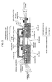
FIG. 1 is a cross-sectional view of a connection structure connecting an RF module and a waveguide according to a first exemplary embodiment of the present invention. - [
FIG. 2 ]
FIG. 2 is a cross-sectional view of a connection structure connecting an RF module and a waveguide according to a second exemplary embodiment of the present invention. - [
FIG. 3 ]
FIG. 3 is a plan view of the connection structure shown inFIG. 2 . - [
FIG. 4 ]
FIG. 4 is a cross-sectional view of a connection structure connecting an RF module and a waveguide according to a third exemplary embodiment of the present invention. - A connection structure according to an exemplary embodiment of the present invention to be explained next includes a first substrate (module substrate) on which an RF circuit section and a transmission line conversion section are put together, a second substrate (mother substrate) in which an opening is formed having a size larger than the opening size of a waveguide, and a waveguide conductor in which the waveguide is formed. The mother substrate is fixed onto the waveguide conductor so as to cause the opening centers of the waveguide and the mother substrate to coincide with each other and the module substrate is fixed onto the mother substrate so as to cover the opening of the mother substrate. A conductor is disposed around the opening of the mother substrate to form a choke shorting face. A choke is formed by utilizing a space among the module substrate, the mother substrate, and the waveguide so as to keep a characteristic necessary for an opening of a waveguide.
- In this manner, by means of forming the opening of the mother substrate which is sufficiently larger than the opening size of the waveguide, an actual opening size can be determined by the conductor of the waveguide, a conductor of the mother substrate, and a conductor of the module substrate, and the mother substrate can be made common among the different frequency bands to be used. Moreover, since a choke structure is formed only by means of mounting a module substrate and a waveguide each having an opening corresponding to a frequency band to be used on the mother substrate having the large opening, it is possible to perform waveguide connection by a simple process without causing characteristic deterioration. In the following, embodiments of the present invention will be explained with reference to the drawings.
- As shown in
FIG. 1 , in an RF module connection structure according to a first exemplary embodiment of the present invention, a module substrate 1 is surface-mounted onto amother substrate 2, and themother substrate 2 is fixed with ascrew 13 to aconductor 8 serving as a tube wall of awaveguide 3. Thereby, theconductor 8 is fixed so as to function as electrical ground GND for themother substrate 2 and also not to cause a gap. However, because of thickness variation of themother substrate 2, a soldering state and warpage of the module substrate 1, and the like, it is difficult to cause theconductor 8 also to contact the module substrate 1 which is surface-mounted on themother substrate 2, without a gap. Conversely, since it is easy to perform design so as to intentionally cause a gap to be generated between the module substrate 1 and theconductor 8, by designing this gap as a choke to form a choke flange, it is possible to perform waveguide connection preferably. In the following, the configuration of each part will be explained. - An RF circuit section and a transmission line conversion section are put together on the module substrate 1. The RF circuit section includes an amplifier, a matching circuit, and the like, and the circuit size thereof may depend on an apparatus design. The transmission line conversion section is configured with a back short 7 which is formed by means of cutting out a
conductor 6 in a part having the same size as the opening size of thewaveguide 3, and astrip conductor 9.Electronic parts 11 are mounted on the module substrate 1. Theelectronic parts 11 are RF circuit parts and include an amplifier, a matching circuit, and the like. InFIG. 1 , while a shield of the back short 7 and theelectronic parts 11 is integrally formed by theconductor 6, it is not necessarily integrally formed, and the shield of theelectronic parts 11 may be formed as needed also for each of the parts. - Further, the module substrate 1 is a multi-layered substrate, and is configured here with
conductor layers 1a to 1d andinsulating layers 1e to 1f therebetween. The aboveelectronic parts 11 are mounted on thetop conductor layer 1a, and thestrip conductor 9 extended from theelectronic parts 11 is formed in a region corresponding to the opening of thewaveguide 3. In each of theother conductor layers 1b to 1d, a conductor is not formed in the region corresponding to the opening of thewaveguide 3. The module substrate 1 is attached to themother substrate 2 in alignment with the opening of themother substrate 2 by a method such as soldering. The layers between thetop conductor layer 1 a and thebottom conductor layer 1 d are connected electrically to one other by via-holes or the like, and connected here to theconductor 8 which is equivalent to GND through via-holes of themother substrate 2. Note that, the number of the conductor layers of the module substrate 1 depends on a design requirement and theconductor layers 1 a to 1 d shown inFIG. 1 are one example. - An opening for the waveguide connection is formed in the
mother substrate 2 with a size larger than the opening size d of the waveguide, and aconductor plating layer 5a is formed on the edge face of the opening of themother substrate 2 in contact with aconductor layer 2d. Themother substrate 2 is fixed to theconductor 8 by thescrew 13. Further,electronic parts 12 are mounted on themother substrate 2. Theelectronic parts 12 include a CPU, a power supply circuit, an IF circuit, and the like. Further, themother substrate 2 is a multi-layered substrate, and, while aconfiguration including conductors 2a to 2d andinsulating layers 2e to 2f therebetween is illustrated, the number of the conductor layers depends on a design requirement. Note that each of the opening of thewaveguide 3 and the opening of themother substrate 2 is rectangular or circular. - The
waveguide 3 and anannular groove 4 are integrally formed in theconductor 8. Themother substrate 2 and the module substrate 1 are fixed so as to cover thewaveguide 3 of theconductor 8, and thereby a choke is configured with theannular groove 4, theconductor 1d of the module substrate 1, theconductor plating layer 5a and theconductor layer 2d of themother substrate 2. While preferably the via-holes 10 are formed as close as possible to the opening end face of themother substrate 2, the positions thereof are determined by design. - As described above, the choke is configured with the
annular groove 4, theconductor layer 1d of the module substrate 1, theconductor plating layer 5a and theconductor layer 2d of themother substrate 2. Accordingly, by setting the effective distance from the wall face of thewaveguide 3 to the deepest face 5 of theannular groove 4 to be half a wavelength λg (t = λg /2) inside the waveguide, it is possible to manufacture a connection structure having a small loss or leakage of a high frequency signal in a desired frequency band to be used, in a simple process. - Note that the via-
hole 10 may be filled with a conductor as a build-up via. In the case of the build-up via, even if the deepest face 5 of theannular groove 4 is extended to under the via-hole 10, the choke characteristic is not affected. Accordingly, there is an advantage that design restriction does not exist. - In the above first exemplary embodiment, as shown in
FIG. 1 , the choke is configured with theannular groove 4, theconductor layer 1d of the module substrate 1, and theconductor plating layer 5a and theconductor layer 2d of themother substrate 2. However, the present invention is not limited to this configuration. As shown inFIG. 2 , the choke can be also configured using the via-holes 10 instead of theconductor plating layer 5a. Hereinafter, a second exemplary embodiment of the present invention will be explained with reference toFIG. 2 andFIG. 3 , provided that the configuration except the choke is the same as that of the first exemplary embodiment shown inFIG. 1 , and the same reference number is attached and explanation will be omitted. In the following, explanation will be provided focusing on a choke configuration. - In
FIG. 3 , the via-holes 10 are provided so as to surround the opening of themother substrate 2 at predetermined intervals (preferably at intervals not larger than 1/4 of a signal wavelength, and, while a better characteristic is obtained as the intervals are smaller (e.g., 1/40), these intervals depend on a design condition), and these arranged via-holes 10 form achoke shorting face 5b. That is, inFIG. 2 , the choke is configured with theannular groove 4, theconductor layer 1 d of the module substrate 1, and the via-holes 10. By appropriately designing the distance from the wall face of thewaveguide 3 to thechoke shorting face 5b, it is possible to manufacture a connection structure having a small loss and leakage of a high frequency signal in a desired frequency band to be used, as in the first exemplary embodiment. - In the above first and second exemplary embodiments, as shown in
FIG. 1 andFIG. 2 , the choke is configured by means of forming theannular groove 4 around thewaveguide 3 in theconductor 8. However, if a characteristic such as a bandwidth which is required for the transmission line conversion allows, it is also possible to form the choke by a simplified annular groove 4a as shown inFIG. 4 and the via-holes 10. When the configuration is simplified in this manner, it is expected to make the process of theconductor 8 easy and to obtain yield improvement and cost reduction. - Specifically, as shown in
FIG. 4 , in an RF module connection structure according to the present embodiment, a choke is formed using as an annular groove 4a a space formed by thewaveguide 3, the opening of themother substrate 2 and the module substrate 1 thereabove without forming the groove in theconductor 8 in which thewaveguide 3 is formed. That is, the choke is configured with theconductor 8, theconductor layer 1 d of the module substrate 1, and conductors in the via-holes 10 of themother substrate 2. The arrangement of the via-holes 10 is as illustrated inFIG. 3 . - Further, a conductor 6a configuring the back short 7 may be provided separately, and a
conductor 14 may be formed for shielding the circuit by theelectronic parts 11 and the circuit by theelectronic parts 12. Note that, since the other members are the same as those of the embodiments shown inFIG. 1 andFIG. 2 , the same reference numbers are provided and their explanations will be omitted. - Also in the present embodiment, by appropriately designing the distance from the wall face of the
waveguide 3 to thechoke shorting face 5b, it is possible to manufacture a connection structure having a small loss and leakage of a high frequency signal in a desired frequency band to be used, in a simple process. At this time, since the groove is not formed in theconductor 8 in which thewaveguide 3 is formed and the choke is configured using the opening of themother substrate 2 and the via-holes 10, it is possible to further simplify the manufacturing process. - According to the above-mentioned embodiments of the present invention, by providing the RF circuit and the transmission line conversion section for the module substrate 1 and providing an opening larger than the opening size of the waveguide for the
mother substrate 2 at a position corresponding to the position where the module substrate 1 is attached, it is possible to reduce frequency-dependent design factors of themother substrate 2, and to make themother substrate 2 common without being limited to a frequency band to be used. - The present invention can be applied generally to a high frequency apparatus which requires a connection between a wiring substrate and a waveguide.
-
- 1 Module substrate
- 1 a to 1 d Conductor layer
- 1e to 1g Insulating layer
- 2 Mother substrate
- 2a to 2d Conductor layer
- 2e to 2g Insulating layer
- 3 Waveguide
- 4, 4a Annular groove
- 5 Deepest part of an annular groove
- 5a Plating layer
- 5b Choke shorting face
- 6, 6a Conductor in back short side
- 7 Back short
- 8 Conductor in waveguide side
- 9 Strip conductor
- 10 Via-hole
- 11 Electronic parts
- 12 Electronic parts
- 13 Screw
- 14 Conductor
Claims (8)
- A connection structure for connecting a high frequency circuit and a waveguide, comprising:a first substrate on which the high frequency circuit is mounted and a transmission line conversion means is provided between the high frequency circuit and the waveguide;a waveguide conductor in which the waveguide is formed; anda second substrate which is provided on the waveguide conductor and has an opening having a size larger than an opening size of the waveguide,wherein the first substrate is fixed onto the second substrate so as to cover the opening of the second substrate, and a choke is formed utilizing a space among the first substrate, the second substrate, and the waveguide conductor.
- The connection structure according to claim 1, wherein
the choke includes the waveguide conductor, a conductor layer of the first substrate, and a conductor passing through the second substrate. - The connection structure according to claim 2, wherein
a plurality of the conductors passing through the second substrate is disposed around the opening of the second substrate at predetermined intervals. - The connection structure according to claim 2 or 3, wherein
a distance between an inner wall of the waveguide and the conductor passing through the second substrate is set to half a wavelength inside the waveguide. - A manufacturing method of a connection structure for connecting a high frequency circuit and a waveguide, comprising the steps of:providing a first substrate on which the high frequency circuit is mounted and a transmission line conversion means is provided between the high frequency circuit and the waveguide, a waveguide conductor in which the waveguide is formed, and a second substrate including an opening having a size larger than an opening size of the waveguide;fixing the second substrate onto the waveguide conductor so as to cause opening centers of the waveguide and the second substrate to coincide with each other;fixing the first substrate onto the second substrate so as to cover the opening of the second substrate; andforming a choke among the first substrate, the second substrate, and the waveguide conductor.
- The manufacturing method of a connection structure according to claim 5, wherein
the choke includes the waveguide conductor, a conductor layer of the first substrate, and a conductor passing through the second substrate. - The manufacturing method of a connection structure according to claim 6, wherein
a plurality of the conductor passing through the second substrate is disposed around the opening of the second substrate at predetermined intervals. - The manufacturing method of a connection structure according to claim 6 or 7, wherein
a distance between an inner wall of the waveguide and the conductor passing through the second substrate is set to half a wavelength inside the waveguide.
Applications Claiming Priority (2)
| Application Number | Priority Date | Filing Date | Title |
|---|---|---|---|
| JP2012099655 | 2012-04-25 | ||
| PCT/JP2013/002730 WO2013161279A1 (en) | 2012-04-25 | 2013-04-23 | Connection structure connecting high frequency circuit and waveguide, and manufacturing method for same |
Publications (2)
| Publication Number | Publication Date |
|---|---|
| EP2843759A1 true EP2843759A1 (en) | 2015-03-04 |
| EP2843759A4 EP2843759A4 (en) | 2015-12-09 |
Family
ID=49482622
Family Applications (1)
| Application Number | Title | Priority Date | Filing Date |
|---|---|---|---|
| EP13781138.6A Withdrawn EP2843759A4 (en) | 2012-04-25 | 2013-04-23 | Connection structure connecting high frequency circuit and waveguide, and manufacturing method for same |
Country Status (5)
| Country | Link |
|---|---|
| US (1) | US9450282B2 (en) |
| EP (1) | EP2843759A4 (en) |
| CN (1) | CN104254945B (en) |
| IN (1) | IN2014DN09553A (en) |
| WO (1) | WO2013161279A1 (en) |
Families Citing this family (5)
| Publication number | Priority date | Publication date | Assignee | Title |
|---|---|---|---|---|
| DE112015005575T5 (en) * | 2014-12-12 | 2017-09-28 | Sony Corporation | MICROWAVE ANTENNA DEVICE, UNIT AND MANUFACTURING METHOD |
| CN108475833A (en) * | 2016-01-20 | 2018-08-31 | 索尼公司 | Connector modules, communication board and electronic device |
| US10992022B2 (en) | 2016-04-01 | 2021-04-27 | Sony Corporation | Microwave antenna apparatus, packing and manufacturing method |
| WO2019053823A1 (en) * | 2017-09-13 | 2019-03-21 | 三菱電機株式会社 | Dielectric filter |
| US10804591B1 (en) * | 2019-04-10 | 2020-10-13 | Jabil Inc. | Side mounting of MEMS microphones on tapered horn antenna |
Family Cites Families (13)
| Publication number | Priority date | Publication date | Assignee | Title |
|---|---|---|---|---|
| JP4261726B2 (en) | 2000-03-15 | 2009-04-30 | 京セラ株式会社 | Wiring board, and connection structure between wiring board and waveguide |
| JP2003078310A (en) * | 2001-09-04 | 2003-03-14 | Murata Mfg Co Ltd | High-frequency line converter, component, module and communication device |
| FR2879830B1 (en) * | 2004-12-20 | 2007-03-02 | United Monolithic Semiconduct | MINIATURE ELECTRONIC COMPONENT FOR MICROWAVE APPLICATIONS |
| JP4375310B2 (en) * | 2005-09-07 | 2009-12-02 | 株式会社デンソー | Waveguide / stripline converter |
| DE102007021615A1 (en) * | 2006-05-12 | 2007-11-15 | Denso Corp., Kariya | Dielectric substrate for a waveguide and a transmission line junction using this |
| JP4584193B2 (en) | 2006-06-15 | 2010-11-17 | 三菱電機株式会社 | Waveguide connection structure |
| JP5115026B2 (en) | 2007-03-22 | 2013-01-09 | 日立化成工業株式会社 | Triplate line-waveguide converter |
| JP5072968B2 (en) | 2007-08-02 | 2012-11-14 | 三菱電機株式会社 | Waveguide connection structure |
| JP2009111837A (en) | 2007-10-31 | 2009-05-21 | Japan Radio Co Ltd | Through-substrate waveguide |
| JP2009296491A (en) | 2008-06-09 | 2009-12-17 | Nec Corp | Waveguide connection structure and semiconductor device |
| US8680954B2 (en) | 2008-08-29 | 2014-03-25 | Nec Corporation | Waveguide, waveguide connection structure and waveguide connection method |
| JP5383796B2 (en) | 2009-04-28 | 2014-01-08 | 三菱電機株式会社 | Connection structure for waveguide converter, method for manufacturing the same, and antenna device using the connection structure |
| US8912858B2 (en) * | 2009-09-08 | 2014-12-16 | Siklu Communication ltd. | Interfacing between an integrated circuit and a waveguide through a cavity located in a soft laminate |
-
2013
- 2013-04-23 WO PCT/JP2013/002730 patent/WO2013161279A1/en not_active Ceased
- 2013-04-23 CN CN201380021963.3A patent/CN104254945B/en not_active Expired - Fee Related
- 2013-04-23 EP EP13781138.6A patent/EP2843759A4/en not_active Withdrawn
- 2013-04-23 US US14/397,048 patent/US9450282B2/en not_active Expired - Fee Related
-
2014
- 2014-11-13 IN IN9553DEN2014 patent/IN2014DN09553A/en unknown
Also Published As
| Publication number | Publication date |
|---|---|
| EP2843759A4 (en) | 2015-12-09 |
| IN2014DN09553A (en) | 2015-07-17 |
| WO2013161279A1 (en) | 2013-10-31 |
| US20150109068A1 (en) | 2015-04-23 |
| US9450282B2 (en) | 2016-09-20 |
| CN104254945B (en) | 2016-08-24 |
| CN104254945A (en) | 2014-12-31 |
Similar Documents
| Publication | Publication Date | Title |
|---|---|---|
| US10128556B2 (en) | Transition between a SIW and a waveguide interface | |
| EP3780259B1 (en) | Transition structure and multilayer transition structure for millimeter wave | |
| US8358185B2 (en) | Waveguide connection between a dielectric substrate and a waveguide substrate having a choke structure in the dielectric substrate | |
| US10295652B2 (en) | Vehicle radar system for detecting the surroundings | |
| US10582608B2 (en) | Interconnection between printed circuit boards | |
| US10299368B2 (en) | Surface integrated waveguides and circuit structures therefor | |
| EP3065213B1 (en) | Dielectric-filled surface-mounted waveguide devices and methods for coupling microwave energy | |
| EP2843759A1 (en) | Connection structure connecting high frequency circuit and waveguide, and manufacturing method for same | |
| US8952266B2 (en) | Structural body and interconnect substrate | |
| US20110037531A1 (en) | Waveguide transition arrangement | |
| US8913397B2 (en) | Power source control circuit module | |
| US10534147B2 (en) | Optical transceiver | |
| US9620851B2 (en) | Wireless communication device and electronic device | |
| US10992015B2 (en) | Coupling comprising a guide member embedded within a blind via of a post-wall waveguide and extending into a hollow tube waveguide | |
| US20170288299A1 (en) | Antenna device | |
| RU2673059C2 (en) | Antenna array feeding structure having circuit boards connected by at least one solderable pin | |
| US20230026891A1 (en) | Semiconductor device and method for manufacturing semiconductor device | |
| EP3080864B1 (en) | System comprising a coaxial cable and a connector for coupling said coaxial cable to a strip line | |
| US9699888B2 (en) | Circuit substrate and electronic device | |
| US10777899B2 (en) | Transmission line coupling system | |
| WO2014189105A1 (en) | Millimeter-wave module | |
| JP2009303076A (en) | Waveguide connection structure | |
| EP3444891A1 (en) | Circuit board and communication device with side coupler | |
| JP5484452B2 (en) | Angled conversion from microstrip line to rectangular waveguide. | |
| US20210135329A1 (en) | Implementation of inductive posts in an siw structure and production of a generic filter |
Legal Events
| Date | Code | Title | Description |
|---|---|---|---|
| PUAI | Public reference made under article 153(3) epc to a published international application that has entered the european phase |
Free format text: ORIGINAL CODE: 0009012 |
|
| 17P | Request for examination filed |
Effective date: 20141107 |
|
| AK | Designated contracting states |
Kind code of ref document: A1 Designated state(s): AL AT BE BG CH CY CZ DE DK EE ES FI FR GB GR HR HU IE IS IT LI LT LU LV MC MK MT NL NO PL PT RO RS SE SI SK SM TR |
|
| AX | Request for extension of the european patent |
Extension state: BA ME |
|
| DAX | Request for extension of the european patent (deleted) | ||
| RA4 | Supplementary search report drawn up and despatched (corrected) |
Effective date: 20151109 |
|
| RIC1 | Information provided on ipc code assigned before grant |
Ipc: H01P 5/107 20060101AFI20151103BHEP Ipc: H01P 11/00 20060101ALI20151103BHEP |
|
| STAA | Information on the status of an ep patent application or granted ep patent |
Free format text: STATUS: THE APPLICATION HAS BEEN WITHDRAWN |
|
| 18W | Application withdrawn |
Effective date: 20170110 |