EP2841997B1 - Dark field diffraction based overlay - Google Patents
Dark field diffraction based overlay Download PDFInfo
- Publication number
- EP2841997B1 EP2841997B1 EP13717625.1A EP13717625A EP2841997B1 EP 2841997 B1 EP2841997 B1 EP 2841997B1 EP 13717625 A EP13717625 A EP 13717625A EP 2841997 B1 EP2841997 B1 EP 2841997B1
- Authority
- EP
- European Patent Office
- Prior art keywords
- dark field
- field image
- overlay
- overlay target
- pad
- Prior art date
- Legal status (The legal status is an assumption and is not a legal conclusion. Google has not performed a legal analysis and makes no representation as to the accuracy of the status listed.)
- Active
Links
Images



Classifications
-
- G—PHYSICS
- G03—PHOTOGRAPHY; CINEMATOGRAPHY; ANALOGOUS TECHNIQUES USING WAVES OTHER THAN OPTICAL WAVES; ELECTROGRAPHY; HOLOGRAPHY
- G03F—PHOTOMECHANICAL PRODUCTION OF TEXTURED OR PATTERNED SURFACES, e.g. FOR PRINTING, FOR PROCESSING OF SEMICONDUCTOR DEVICES; MATERIALS THEREFOR; ORIGINALS THEREFOR; APPARATUS SPECIALLY ADAPTED THEREFOR
- G03F7/00—Photomechanical, e.g. photolithographic, production of textured or patterned surfaces, e.g. printing surfaces; Materials therefor, e.g. comprising photoresists; Apparatus specially adapted therefor
- G03F7/70—Microphotolithographic exposure; Apparatus therefor
- G03F7/70483—Information management; Active and passive control; Testing; Wafer monitoring, e.g. pattern monitoring
- G03F7/70605—Workpiece metrology
- G03F7/70616—Monitoring the printed patterns
- G03F7/70633—Overlay, i.e. relative alignment between patterns printed by separate exposures in different layers, or in the same layer in multiple exposures or stitching
Definitions
- the invention relates to an optical metrology of overlay error and more particularly to measuring diffraction based overlay error.
- Semiconductor processing for forming integrated circuits requires a series of processing steps. These processing steps include the deposition and patterning of material layers such as insulating layers, polysilicon layers, and metal layers.
- the material layers are typically patterned using a photoresist layer that is patterned over the material layer using a photomask or reticle.
- the photomask has alignment targets or keys that are aligned to fiduciary marks formed in the previous layer on the substrate.
- This overlay metrology problem becomes particularly difficult at submicrometer feature sizes where overlay alignment tolerances are reduced to provide reliable semiconductor devices.
- One type of overlay measurement is known as diffraction based overlay metrology.
- diffraction based overlay metrology uses bright field optics in which specular light, i.e., 0 th diffraction order, is used to determine an overlay error.
- specular light i.e., 0 th diffraction order
- dark field optics which uses non-specular light to determine the overlay error.
- targets used in bright field and dark field diffraction based overlay metrology are not interchangeable.
- Prior art document US 2011/043791 A1 discloses one such metrology apparatus arranged to illuminate a plurality of targets with an off-axis illumination mode. Images of the targets are obtained using only one first order diffracted beam. Where the target is a composite grating, overlay measurements can be obtained from the intensities of the images of the different gratings. This document teaches that some overlay measurements can be corrected for errors caused by variations in the position of the gratings in an image field.
- Prior art document US 7508976 B1 discloses a diffraction based overlay metrology system that produces overlay error independent of effects caused by local process variations.
- overlay patterns include process variations that provide spectral contributions, along with the overlay shift, to the measured overlay error.
- the contributions from process variations are removed from the determined overlay error by measuring the overlay pattern before and after the top diffraction gratings are formed.
- a plurality of differential spectra from the measurement locations of the completed overlay pattern can then be used with a plurality of ratios of differential spectra from measurement locations of the incomplete overlay pattern can then be used to determine the overlay error by either direct calculation or by fitting techniques.
- prior art document US 2008/239318 A1 discloses a method of measuring asymmetry in a scatterometer wherein a target portion is illuminated twice, first with 0 DEG of substrate rotation and secondly with 180 DEG of substrate rotation. This prior art document teaches that one of the images is then rotated and subtracted from the other image. In this way, asymmetry of the scatterometer can be corrected.
- a dark field diffraction based overlay metrology device illuminates an overlay target that has at least three pads for an axis, the three pads have different programmed offsets.
- the overlay target may be illuminated using two obliquely incident beams of light from opposite azimuth angles or using normally incident light.
- Two dark field images of the overlay target are collected using ⁇ 1 st diffraction orders to produce at least six independent signals from the overlay target.
- the +1 st diffraction order may be collected from one obliquely incident beam of light and the -1 st diffraction order may be collected from the other obliquely incident beam of light.
- the ⁇ 1 st diffraction orders may be separately detected from the normally incident light to produce the two dark field images of the overlay target.
- the six independent signals from the overlay target are used to determine an overlay error for the sample along the axis.
- Claim 1 recites an overlay metrology method according to a first aspect of the invention.
- Claim 13 recites an overlay metrology device according to a second aspect of the invention.
- Fig. 1 illustrates a dark field diffraction based overlay metrology device 100.
- the metrology device 100 measures the overlay error using one or more overlay targets with three or more pads per axis, which eliminates zero-sensitivity problems in overlay measurements and may eliminate sensitivity to film thickness or its variation in the resulting overlay measurement.
- the metrology device 100 acquires dark field images of an overlay target with at least three pads, which have different programmed offsets, and uses the ⁇ 1 st diffraction orders separately to produce six nominally independent signals for each axis.
- the six independent signals may be used to yield a plurality of overlay error solutions, such that at least two of the overlay error solutions have a measurement null for different structure parameters. Accordingly, the overlay error solutions may be used together, i.e., individually or in combination, to eliminate the zero sensitivity problem.
- the metrology device 100 is a high numerical aperture (NA) optical imaging system.
- An overlay target 120 on a sample 101 is placed in the object plane of the metrology device 100.
- a dark field image of the overlay target 120 is formed in the image plane, which is detected by one or more image sensors to detect the intensity distribution of the image.
- the metrology device 100 uses oblique incidence light that is incident over all the pads of the overlay target 120.
- the light source 102 for the metrology device 100 may be e.g., a monochromatic light source, such as a laser, or a polychromatic light source, such as an arc lamp. If desired, multiple wavelengths, e.g., from one or more light sources may be used for different types of materials.
- the light source 102 produces a first light beam 103 that is incident on the sample 101 at an oblique angle, e.g., between 0° to 80°, e.g., 73°.
- the beam path of the light source 102 may include optical elements, such as an attenuator 104, half-wave plate 106, polarizer 108, doublet lens 110 and a window 112. Fewer, additional or alternative optical elements may be used in the light source beam path.
- the selection of the polarization state, e.g., TE (s-polarization) or TM (p-polarization) of polarizer 108 may be determined empirically based on the structure of the overlay target.
- the light beam 103 is incident on a diffraction overlay target 120 on sample 101, which is held on a stage 122.
- the gratings in each pad of the overlay target 120 diffract the incoming illumination light.
- the metrology device 100 includes dark field imaging optics and at least one detector to collect dark field images of the overlay target 120.
- Each pad in the overlay target 120 diffracts a part of the illuminating light beam 103 and the +1 st diffraction order is collected by the objective lens 124.
- the objective lens 124 may be, e.g., catadioptic, catoptic, or dioptric or any other type of lens system.
- the diffracted light passes through an imaging beam path including several additional optical elements, including a lens 125, an optional field aperture 126, one or more lenses 128, a pupil aperture plate 130, one or more lenses 132, beam splitter 134, lens 136, and a fold mirror assembly 138.
- the imaging beam path is configured to produce a dark field image at the image plane, which is of the overlay target 120, which is received by a detector 140 via the fold mirror assembly 138.
- metrology device 100 is able to capture signals from all three pads in the overlay target simultaneously, which is advantageous to increase throughput.
- conventional DBO systems typically image the pupil plane, and thus, must separately probe each pad in an overlay target. Consequently, conventional DBO systems require movement of the sample and/or field aperture to separately probe each pad which adversely effects throughput and requires relatively large pads that can be individually probed by the illuminating light.
- a beam splitter 134 splits a portion of the diffracted light and images the pupil aperture plate 130 located at the pupil plane of the imaging system on a separate detector 142 via lens 144 and optional iris 146.
- the image of the pupil aperture plate 130 on detector 142 may be used to determine whether the angle of incidences of the beams 103 and 103a are correct and symmetrical, e.g., by analyzing the location of the focused spots in the resulting image of the pupil aperture plate 130.
- the metrology device 100 includes a second light source 102a, which produces the second light beam 103a with the same angle of incidence as the first light beam 103, but with an opposite azimuth angle, i.e., the azimuth angles of light beam 103 and light beam 103 differ by 180°.
- the same angle of incidence and the opposite azimuth angle refer to angles that are nominally the same, as opposed to being precisely the same, where nominally means that the BiDirectional Reflection Distribution Function satisfies the tolerance dictated by the pitch of the gratings and the size of the aperture used.
- the second light beam 103a is diffracted by the overlay target 120 and the -1 st diffraction order is received by objective lens 124, passes through the optical elements including the pupil aperture plate 130 and is received by a detector 140a.
- the overlay target 120 which includes at least three pads, is illuminated in a first direction by the light beam 103 to produce and collect +1 st diffraction order, and is illuminated at the opposite azimuth angle by light source 103a to produce and collect the -1 st diffraction order. It should be understood that Fig.
- the overlay target 120 includes at least three independent pads and, thus, a total of at least six independent signals are captured.
- metrology device 100 may include a third light source 102b and a fourth light source 102c, which are arranged with azimuth angles that are nominally orthogonally to the azimuth angles of the light source 102 and light source 102a, as show in a top view in Fig. 3 .
- the light beams produced by light sources 102b and 102c are similarly diffracted from overlay target 120 or from an orthogonally aligned overlay target, and received by objective lens 124, passes through the optical elements including the pupil aperture plate 130 and are received by one or more detectors.
- a second set of at least six independent signals are captured for the orthogonal axis.
- stage 122 when stage 122 is an R- ⁇ stage, the overlay target 120 may be positioned such that the light sources 102, 102a, 102b, and 102c may have relatively large azimuth angles with respect to the diffraction gratings. Accordingly, when using an R- ⁇ stage it may be desirable to include an additional set of four orthogonal light sources that are oriented 45° with respect to light sources 102, 102a, 102b, and 102c, to ensure that the ⁇ 1 st diffraction order light is collected by the imaging systems, which has a limited NA. When eight light sources are used with metrology device 100, it may be advantageous to use a single detector.
- Fig. 1 Separate detectors 140 and 140a are illustrated in Fig. 1 , however, if desired, the detectors may be combined into a single detector, as illustrated by detector 141 in Fig. 4.
- Fig. 4 illustrates pupil aperture plate 130, lenses 132, beam splitter 134 and lens 136.
- a single detector 141 is used instead of using fold mirror assembly 138, 139 and multiple detectors being used. With use of a single detector 141, the +1 st diffraction order and the -1 st diffraction order from the overlay target 120 are captured by the detector 141 sequentially.
- Fig. 5 illustrates the pupil aperture plate 130 that may be used in the dark field imaging optics of the dark field diffraction based overlay metrology device 100.
- the pupil aperture plate 130 includes a plurality off-center apertures 131, 131a, 131b, and 131c, through which the diffracted light resulting from light sources 102, 102a, 102b, and 102c, respectively, passes.
- a pupil aperture plate 130' may include a single annular aperture 131' instead of a plurality of separate apertures. The use of a single annular aperture 131' may be particularly useful when stage 122 is an R- ⁇ stage, as opposed to an XY stage.
- the detectors of metrology device 100 are coupled to a computer 150, which analyzes the data provided by the detectors.
- Computer 150 includes a processor 152 with memory 154, as well as a user interface including e.g., a display 158 and input devices 160.
- a non-transitory computer-usable medium 162 having computer-readable program code embodied may be used by the computer 150 for causing the processor to control the metrology device 100 and to perform the functions including the analysis described herein.
- a computer readable storage medium 162 which may be any device or medium that can store code and/or data for use by a computer system such as processor 152.
- the non-transitory computer-usable medium 162 may be, but is not limited to, magnetic and optical storage devices such as disk drives, magnetic tape, compact discs, and DVDs (digital versatile discs or digital video discs).
- a communication port 164 may also be used to receive instructions that are used to program the computer 150 to perform any one or more of the functions described herein and may represent any type of communication connection, such as to the internet or any other computer network.
- ASIC application specific integrated circuit
- PLD programmable logic device
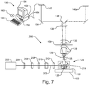
- Fig. 7 illustrates another implementation of a dark field diffraction based overlay metrology device 200, which is similar to metrology device 100 shown in Fig. 1 , like designated elements being the same, but in which normal incidence light is used instead of oblique incidence light.
- normal incidence illumination may be provided with a light source 202, which produces a light beam 203 that is reflected by fold mirror 214 to be normally incident on the overlay target 120.
- the beam path of the light source 202 may include optical elements, such as an attenuator 204, half-wave plate 206, polarizer 208, doublet lens 210 and a window 212, similar to metrology device 100 shown in Fig. 1 . Fewer, additional or alternative optical elements may be used in the light source beam path.
- the overlay target 120 is illuminated by the normal incidence light beam 203 resulting in the production of the +1 st diffraction order and the -1 st diffraction order.
- the normal incidence metrology device 200 collects the dark field images produced by the ⁇ 1 st diffraction orders, similar to metrology device 100 described above.
- Metrology device 100 is a diffraction based overlay measurement system and thus, the overlay target 120 is made of gratings that diffract the illumination light to produce the overlay error signal.
- the overlay target 120 includes gratings that overlie each other on the process layers.
- overlay target 120 includes multiple (at least three) target pads, each of which includes two overlaying grating pairs (one grating on each process layer). The overlay error is determined by measuring the relative lateral distance between the gratings pairs in the overlay target 120.
- Fig. 8 illustrates the overlay target 120, which is used for a single direction, e.g., the X coordinate axis.
- a similar overlay target, but orthogonally aligned to overlay target 120 may be used for the orthogonal direction, e.g., the Y coordinate axis.
- the overlay target 120 is illustrated as including three pads, labeled A, B, and C. Each pad includes two interleaved gratings 171 and 172, which are associated with separate process steps and may be deposited on overlaying layers (which may be directly overlaying or may include one or more intervening layer) or may be deposited on the same layer.
- the overlay target 120 includes three pads, each having a different programmed offset. As illustrated in Fig. 8 , pads A and C, having equal but opposite programmed offsets, i.e., pad A has an offset of + d + ⁇ , while pad C has an offset of -d + ⁇ , where ⁇ is the overlay error and
- overlay target 120 may have a folding symmetry along the direction of measurement, e.g., the X coordinate axis. Folding symmetry in overlay target 120, however, is not required and may be avoided, e.g., by rearranging the pads A and B or pads B and C, or alternatively by providing a programmed offset in pad B and/or different magnitude programmed offsets in pads A and C. Additionally, the pads may all have programmed offsets in the same direction but different magnitudes. Additionally, additional pads may be used in overlay target, where at least three of the pads have different programmed offsets. Fig.
- d a and d d may be equal in magnitude and opposite in direction, while d b and d c are equal in magnitude and opposite in direction, but differ from d a and d d .
- the use of at least three pads in the overlay target each having different programmed offsets is advantageous at it permits measurement of overlay error by the metrology device 100 or 200 with a minimum (potentially no) zero-sensitivity problems in overlay measurements and may eliminate sensitivity to film thickness or its variation in the resulting overlay measurement.
- the metrology devices 100 and 200 capture dark field images with the ⁇ 1 st diffraction orders from each of the pads in the overlay target 120 using obliquely incident or normally incident light. It should be understood, that the dark field images may not resolve the grid lines within the pads of the overlay target 120, but may provide an intensity level associated with each of pad.
- Fig. 10 illustrates a dark field image 220 of the overlay target 120 captured using the - 1 st diffraction order and a dark field image 222 of the overlay target 120 captured using the +1 st diffraction order. As illustrated in Fig.
- the grid lines in the pads of the overlay target 120 are not resolved in the dark field images 220 and 222, but the general intensity I for each pad is detected.
- six independent signals for the overlay target 120 are acquired, and are labeled in Fig. 10 as I A- , I B- , I C- for dark field image 220 and I A + , I B + , I C + for dark field image 222.
- additional pads may be acquired.
- at least six independent signals are acquired.
- the measurement of overlay error may be based on the following:
- U(x) the complex amplitude of illumination beam on a target, can be expressed as follows.
- ⁇ strongly depends on wavelength and the film thickness between the two interleaving target gratings. It also depends on the height and duty cycle differences between the two target gratings.
- the target is illuminated using a beam of opposite incidence angle to get both ⁇ 1 st diffraction orders, as illustrated in Fig. 1 .
- the two illumination beams may need to be turned on at different times to avoid the interference of diffracted light from the two beams at the detector plane. Additionally, if the beam incidence angle is extremely large, one of the diffraction orders can become evanescent or non-radiative even inside the sample. This can reduce the undesirable high order coupling between the two gratings.
- the overlay information is contained in the last term.
- the first two terms, a 2 + b 2 do not carry overlay information and are a source of photon noise. This means that the signal-to-noise ratio will be highest when the diffraction efficiencies of the two interleaving gratings are the same.
- the intensity of ⁇ 1 st diffraction orders from each target pad A, B, and C, illustrated in overlay target 120 in Fig. 6 can be calculated using equations (4-2) and (4-4) as follows.
- the overlay error ⁇ can be determined from the intensity measurements of the ⁇ 1 st diffraction orders coming from each target pad, e.g., using the equations (5-1) through (7-4). With the six independent signals captured using the ⁇ 1 st diffraction orders and the three target pads from overlay target 120, there are only four unknowns, a, b, ⁇ and ⁇ . Therefore, three independent solutions for ⁇ can be obtained. In order to get the three independent solutions, first, we need to define the following five quantities.
- the intensity values for pads A and C in the first dark field image, designed by "+”, and the second dark field image, designated by "-”, are combined to generate a signal value in the numerator, while intensity values for the three pads A, B, and C in the first dark field image and the second dark field image are combined to generate a reference value in the denominator.
- a value is generated that is proportional to the overlay error.
- the intensity values in the first dark field image (+) and the second dark field image (-) for pad B are combined to generate a signal value in the numerator, while intensity values in the first dark field image and the second dark field image for pad A and for pad C are combined to generate a reference value in the denominator.
- a value is generated that is proportional to the overlay error.
- the last solution (10-3) does not require the middle target pad and needs only the two outer target pads A and C, illustrated in Fig. 6 .
- the robustness of each individual solution depends critically on the film thickness between the two interleaving target gratings in the overlay target 120.
- the overlay error solutions are used together, i.e., individually or in combination, to eliminate the zero sensitivity problem.
- the present embodiment may solve the problem elegantly by combining the separate solutions in complex plane because Q 1 is proportional to cos( ⁇ ) while Q 2 and Q' 2 are proportional to sine( ⁇ ) and cos( ⁇ ) and sin( ⁇ ) form a quadrature in complex plane. Therefore, the problem can be overcome using a weighted quadrature combination in the complex plane. In order to do that, we define the following two complex quantities.
- ⁇ , ⁇ , ⁇ are weights chosen . Only two of them are independent .
- Equation (12-1) (or (12-2)) is the most general expression for overlay error ⁇ .
- the best values for the weights, ⁇ , ⁇ and ⁇ will be different for different cases. They can also be different across the wafer. They can be different even across a single die if multiple targets are printed inside a single die. However, they can be determined through simulations or experiments. An appropriate change of the weights, as determined empirically or experimentally, across the wafer or die can improve the accuracy of overlay measurements. Note that only two of the three weights, ⁇ , ⁇ and ⁇ , are independent because dividing or multiplying the numerator and denominator of equations (12-1) and (12-2) simultaneously with a non-zero number does not affect the overlay result.
- the real and imaginary parts of equations (11-1) and (11-2) cannot be zero simultaneously as long as ⁇ and ⁇ + ⁇ are chosen to be non-zero. Therefore, equation (12-1) or (12-2) can produce reliable overlay error results even with illuminating light of a single wavelength regardless of film thickness change or variation between the two interleaving target gratings.
- the equations also work for the no film case such as double patterning; they do not require different duty cycles for the two interleaving target gratings even in the double patterning case. They can produce a reliable overlay error results with any grating duty cycle. This kind of low or no sensitivity to film thickness change or variation even with single wavelength is advantageous with respect to conventional overlay measurement devices.
- the imaginary part of equation (12-1) or (12-2) must be zero, with real measurement data, however, it can have a small imaginary component. This is not a serious problem as long as the imaginary component is smaller than the overlay measurement error budget. The small imaginary component can be ignored or used to assess how robust the measurement is.
- Equation (12-1) or (12-2) provides the overlay error.
- obtaining the overlay error through the data regression process using the target image model may be better because regression can use all the measured data and can take care of many error sources such as the interference between the images of different target pads, focus error, optical system aberrations, the mixing of diffraction orders due to finite target size, etc.
- the overlay error value obtained from the analytical solution, (12-1) or (12-2) can be used as the starting overlay value in the regression.
- the image modeling in this case is much simpler than optical critical dimension (OCD) modeling because it requires only target pitch and offset information, and does not require target structure information.
- OCD optical critical dimension
- Lasers are one of the preferred sources for small target applications because they are one of the brightest sources.
- the choice of wavelengths is very limited with lasers. Consequently, when lasers are adopted as source, it is hard to avoid the zero-sensitivity pitfalls with the conventional DBO solution with two target pads.
- the present embodiment which does not have zero-sensitivity pitfalls even with single wavelength, is better-suited for laser illuminated DBO applications than conventional solutions.
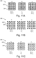
- Figs. 11A, 11B, and 11C illustrates a variation of the overlay target, in which the x- and y-targets pads are combined, thereby reducing the target design from six pads for both the x- and y- overlay measurements, to only three target pads for the x- and y-overlay measurements.
- the use of a combined x and y direction overlay targets may result in the intermixing of the diffracted light for the x- and y- directions. However, this may be avoided by blocking diagonal diffraction orders at the pupil plane using, e.g., pupil aperture plate 130 in Fig. 5 , and/or employing an image model based regression algorithm for signal processing.
- Fig. 11A is an overlay target 320 with three measurement pads A, B, C, that is formed with crate shaped structures 322 in one grating and an array of small boxes 324 in the other grating with folding symmetry in the x- direction and the y-direction.
- the overlay target 230 is well-suited for layer-over-layer overlay measurements because the diffraction efficiencies of crate and box array can be similar if the crate is printed in lower layer and the box array is printed in top layer.
- Fig. 11B illustrates another overlay target 330 with folded symmetry, in which both gratings are made of array of boxes 332 and 334.
- the overlay target 330 is well-suited for double or multiple patterning because the diffraction efficiencies of the two interleaving box-array targets are expected to be similar when they are printed in the same plane during double or multiple patterning process.
- Fig. 11C illustrates another overlay target 340 with folded symmetry, with crates 342 and an array of boxes 344, in which the corners of the crates 342 are open to facilitate an unobstructed flow of photoresist during photoresist coating process. Easier flow of photoresist usually reduces the asymmetry in target structure.
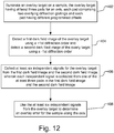
- Fig. 12 is a flow chart illustrating a method of performing dark field diffraction based overlay.
- an overlay target on a sample is illuminated (402).
- the overlay target has at least three pads for an axis.
- Each pad includes two overlaying diffraction gratings, which may be formed on overlaying layers, without or without an intervening layer, or may be overlaying on the same layer.
- Each pad has a different programmed offset.
- a second overlay target may be illuminated for an orthogonal second axis or the overlay target may include pads associated with the second axis.
- the overlay target may be illuminated using two obliquely incident beams of light with the same angles of incidence but opposite azimuth angles, as illustrated in Fig. 1 , or using normally incident light, as illustrated in Fig. 7 .
- a first dark field image of the overlay target using a +1st diffraction order and a second dark field image of the overlay target using a -1st diffraction order are detected (404).
- At least six independent signals are collected for the overlay target from the first dark field image and the second dark field image (406). Each independent signal is collected from one of the at least three pads in the first dark field image and the second dark field image.
- the at least six independent signals from the overlay target are used to determine an overlay error for the sample along the axis (408).
Landscapes
- Physics & Mathematics (AREA)
- General Physics & Mathematics (AREA)
- Length Measuring Devices By Optical Means (AREA)
- Exposure And Positioning Against Photoresist Photosensitive Materials (AREA)
Description
- The invention relates to an optical metrology of overlay error and more particularly to measuring diffraction based overlay error.
- Semiconductor processing for forming integrated circuits requires a series of processing steps. These processing steps include the deposition and patterning of material layers such as insulating layers, polysilicon layers, and metal layers. The material layers are typically patterned using a photoresist layer that is patterned over the material layer using a photomask or reticle. Typically, the photomask has alignment targets or keys that are aligned to fiduciary marks formed in the previous layer on the substrate. However, as the size of integrated circuit features continues to decrease, it becomes increasingly difficult to measure the overlay accuracy of one masking level with respect to the previous level. This overlay metrology problem becomes particularly difficult at submicrometer feature sizes where overlay alignment tolerances are reduced to provide reliable semiconductor devices. One type of overlay measurement is known as diffraction based overlay metrology.
- One type of diffraction based overlay metrology uses bright field optics in which specular light, i.e., 0th diffraction order, is used to determine an overlay error. Another type of diffraction based overlay metrology uses dark field optics, which uses non-specular light to determine the overlay error. Both types of diffraction based overlay metrology uses targets composed of overlying diffraction gratings. However, the targets used in bright field and dark field diffraction based overlay metrology are not interchangeable.
- Prior art document
US 2011/043791 A1 discloses one such metrology apparatus arranged to illuminate a plurality of targets with an off-axis illumination mode. Images of the targets are obtained using only one first order diffracted beam. Where the target is a composite grating, overlay measurements can be obtained from the intensities of the images of the different gratings. This document teaches that some overlay measurements can be corrected for errors caused by variations in the position of the gratings in an image field. - Prior art document
US 7508976 B1 discloses a diffraction based overlay metrology system that produces overlay error independent of effects caused by local process variations. As disclosed in this document, overlay patterns include process variations that provide spectral contributions, along with the overlay shift, to the measured overlay error. The contributions from process variations are removed from the determined overlay error by measuring the overlay pattern before and after the top diffraction gratings are formed. A plurality of differential spectra from the measurement locations of the completed overlay pattern can then be used with a plurality of ratios of differential spectra from measurement locations of the incomplete overlay pattern can then be used to determine the overlay error by either direct calculation or by fitting techniques. - In addition, prior art document
US 2008/239318 A1 discloses a method of measuring asymmetry in a scatterometer wherein a target portion is illuminated twice, first with 0 DEG of substrate rotation and secondly with 180 DEG of substrate rotation. This prior art document teaches that one of the images is then rotated and subtracted from the other image. In this way, asymmetry of the scatterometer can be corrected. - A dark field diffraction based overlay metrology device illuminates an overlay target that has at least three pads for an axis, the three pads have different programmed offsets. By way of example, the overlay target may be illuminated using two obliquely incident beams of light from opposite azimuth angles or using normally incident light. Two dark field images of the overlay target are collected using ±1st diffraction orders to produce at least six independent signals from the overlay target. For example, the +1st diffraction order may be collected from one obliquely incident beam of light and the -1st diffraction order may be collected from the other obliquely incident beam of light. Alternatively, the ±1st diffraction orders may be separately detected from the normally incident light to produce the two dark field images of the overlay target. The six independent signals from the overlay target are used to determine an overlay error for the sample along the axis.
-
Claim 1 recites an overlay metrology method according to a first aspect of the invention. - Claim 13 recites an overlay metrology device according to a second aspect of the invention.
- Further aspects of the invention are recited in the dependent claims.
-
-
Fig. 1 schematically illustrates a side view of a dark field diffraction based overlay metrology device that uses obliquely incident light. -
Figs. 2A and 2B illustrate the generation of ±1st diffraction orders from obliquely incident light and normal incident light, respectively. -
Fig. 3 schematically illustrates a top view of the dark field diffraction based overlay metrology device. -
Fig. 4 illustrates a portion of the imaging beam path of the metrology device using a single detector. -
Fig. 5 illustrates a pupil aperture plate that may be used in the dark field imaging optics of the dark field diffraction based overlay metrology device. -
Fig. 6 illustrates another pupil aperture plate that may be used in the dark field imaging optics of the dark field diffraction based overlay metrology device -
Fig. 7 illustrates another implementation of a dark field diffraction based overlay metrology device that uses normally incident light. -
Fig. 8 illustrates an overlay target that may be used with the dark field diffraction based overlay metrology device. -
Fig. 9 illustrates another overlay target, with an additional pad, that may be used with the dark field diffraction based overlay metrology device. -
Fig. 10 illustrates a dark field images of the overlay target captured using the ±1st diffraction orders. -
Figs. 11A, 11B, and 11C illustrate variations of the overlay target that may be used with the dark field diffraction based overlay metrology device. -
Fig. 12 is a flow chart illustrating a method of performing dark field diffraction based overlay. -
Fig. 1 illustrates a dark field diffraction basedoverlay metrology device 100. Themetrology device 100 measures the overlay error using one or more overlay targets with three or more pads per axis, which eliminates zero-sensitivity problems in overlay measurements and may eliminate sensitivity to film thickness or its variation in the resulting overlay measurement. - Conventional dark field diffraction based overlay metrology devices use a single overlay error solution that has minimum (potentially zero) sensitivity, i.e., measurement null, for particular structure parameters, e.g., when film thicknesses introduce an integral π phase shift in the probe light, which is known as the zero-sensitivity problem. In contrast, the
metrology device 100 acquires dark field images of an overlay target with at least three pads, which have different programmed offsets, and uses the ±1st diffraction orders separately to produce six nominally independent signals for each axis. The six independent signals may be used to yield a plurality of overlay error solutions, such that at least two of the overlay error solutions have a measurement null for different structure parameters. Accordingly, the overlay error solutions may be used together, i.e., individually or in combination, to eliminate the zero sensitivity problem. - The
metrology device 100 is a high numerical aperture (NA) optical imaging system. Anoverlay target 120 on asample 101 is placed in the object plane of themetrology device 100. A dark field image of theoverlay target 120 is formed in the image plane, which is detected by one or more image sensors to detect the intensity distribution of the image. Themetrology device 100 uses oblique incidence light that is incident over all the pads of theoverlay target 120. Thelight source 102 for themetrology device 100 may be e.g., a monochromatic light source, such as a laser, or a polychromatic light source, such as an arc lamp. If desired, multiple wavelengths, e.g., from one or more light sources may be used for different types of materials. Thelight source 102 produces afirst light beam 103 that is incident on thesample 101 at an oblique angle, e.g., between 0° to 80°, e.g., 73°. As illustrated, the beam path of thelight source 102 may include optical elements, such as anattenuator 104, half-wave plate 106,polarizer 108,doublet lens 110 and awindow 112. Fewer, additional or alternative optical elements may be used in the light source beam path. The selection of the polarization state, e.g., TE (s-polarization) or TM (p-polarization) ofpolarizer 108 may be determined empirically based on the structure of the overlay target. - The
light beam 103 is incident on adiffraction overlay target 120 onsample 101, which is held on astage 122. The gratings in each pad of theoverlay target 120 diffract the incoming illumination light. Themetrology device 100 includes dark field imaging optics and at least one detector to collect dark field images of theoverlay target 120. Each pad in theoverlay target 120 diffracts a part of the illuminatinglight beam 103 and the +1st diffraction order is collected by theobjective lens 124. Theobjective lens 124 may be, e.g., catadioptic, catoptic, or dioptric or any other type of lens system. The diffracted light passes through an imaging beam path including several additional optical elements, including alens 125, anoptional field aperture 126, one ormore lenses 128, apupil aperture plate 130, one ormore lenses 132,beam splitter 134,lens 136, and afold mirror assembly 138. The imaging beam path is configured to produce a dark field image at the image plane, which is of theoverlay target 120, which is received by adetector 140 via thefold mirror assembly 138. By imaging theoverlay target 120 at the image plane,metrology device 100 is able to capture signals from all three pads in the overlay target simultaneously, which is advantageous to increase throughput. In comparison, conventional DBO systems typically image the pupil plane, and thus, must separately probe each pad in an overlay target. Consequently, conventional DBO systems require movement of the sample and/or field aperture to separately probe each pad which adversely effects throughput and requires relatively large pads that can be individually probed by the illuminating light. - As illustrated in
Fig. 1 , abeam splitter 134 splits a portion of the diffracted light and images thepupil aperture plate 130 located at the pupil plane of the imaging system on aseparate detector 142 vialens 144 andoptional iris 146. The image of thepupil aperture plate 130 ondetector 142 may be used to determine whether the angle of incidences of thebeams pupil aperture plate 130. - As can be seen, the
metrology device 100 includes a secondlight source 102a, which produces thesecond light beam 103a with the same angle of incidence as thefirst light beam 103, but with an opposite azimuth angle, i.e., the azimuth angles oflight beam 103 andlight beam 103 differ by 180°. It should be understood that the same angle of incidence and the opposite azimuth angle refer to angles that are nominally the same, as opposed to being precisely the same, where nominally means that the BiDirectional Reflection Distribution Function satisfies the tolerance dictated by the pitch of the gratings and the size of the aperture used. Thesecond light beam 103a is diffracted by theoverlay target 120 and the -1st diffraction order is received byobjective lens 124, passes through the optical elements including thepupil aperture plate 130 and is received by adetector 140a. Thus, as illustrated inFig. 2A , theoverlay target 120, which includes at least three pads, is illuminated in a first direction by thelight beam 103 to produce and collect +1st diffraction order, and is illuminated at the opposite azimuth angle bylight source 103a to produce and collect the -1st diffraction order. It should be understood thatFig. 2 illustrates the angle of incidence of thelight beams metrology device 100 uses the same angle of incidence for bothlight beams overlay target 120 are produced from both the +1st diffraction order and the -1st diffraction order. Theoverlay target 120 includes at least three independent pads and, thus, a total of at least six independent signals are captured. - Additionally,
metrology device 100 may include a thirdlight source 102b and a fourthlight source 102c, which are arranged with azimuth angles that are nominally orthogonally to the azimuth angles of thelight source 102 andlight source 102a, as show in a top view inFig. 3 . The light beams produced bylight sources overlay target 120 or from an orthogonally aligned overlay target, and received byobjective lens 124, passes through the optical elements including thepupil aperture plate 130 and are received by one or more detectors. Thus, a second set of at least six independent signals are captured for the orthogonal axis. Additionally, whenstage 122 is an R-θ stage, theoverlay target 120 may be positioned such that thelight sources light sources metrology device 100, it may be advantageous to use a single detector. -
Separate detectors Fig. 1 , however, if desired, the detectors may be combined into a single detector, as illustrated bydetector 141 inFig. 4. Fig. 4 illustratespupil aperture plate 130,lenses 132,beam splitter 134 andlens 136. Instead of usingfold mirror assembly single detector 141 is used. With use of asingle detector 141, the +1st diffraction order and the -1st diffraction order from theoverlay target 120 are captured by thedetector 141 sequentially. -
Fig. 5 illustrates thepupil aperture plate 130 that may be used in the dark field imaging optics of the dark field diffraction basedoverlay metrology device 100. Thepupil aperture plate 130 includes a plurality off-center apertures light sources Fig. 6 , a pupil aperture plate 130' may include a single annular aperture 131' instead of a plurality of separate apertures. The use of a single annular aperture 131' may be particularly useful whenstage 122 is an R-θ stage, as opposed to an XY stage. - The detectors of
metrology device 100 are coupled to acomputer 150, which analyzes the data provided by the detectors.Computer 150 includes aprocessor 152 withmemory 154, as well as a user interface including e.g., adisplay 158 andinput devices 160. A non-transitory computer-usable medium 162 having computer-readable program code embodied may be used by thecomputer 150 for causing the processor to control themetrology device 100 and to perform the functions including the analysis described herein. The data structures and software code for automatically implementing one or more acts described in this detailed description can be implemented by one of ordinary skill in the art in light of the present disclosure and stored, e.g., on a computerreadable storage medium 162, which may be any device or medium that can store code and/or data for use by a computer system such asprocessor 152. The non-transitory computer-usable medium 162 may be, but is not limited to, magnetic and optical storage devices such as disk drives, magnetic tape, compact discs, and DVDs (digital versatile discs or digital video discs). Acommunication port 164 may also be used to receive instructions that are used to program thecomputer 150 to perform any one or more of the functions described herein and may represent any type of communication connection, such as to the internet or any other computer network. Additionally, the functions described herein may be embodied in whole or in part within the circuitry of an application specific integrated circuit (ASIC) or a programmable logic device (PLD), and the functions may be embodied in a computer understandable descriptor language which may be used to create an ASIC or PLD that operates as herein described. -
Fig. 7 illustrates another implementation of a dark field diffraction basedoverlay metrology device 200, which is similar tometrology device 100 shown inFig. 1 , like designated elements being the same, but in which normal incidence light is used instead of oblique incidence light. As illustrated, normal incidence illumination may be provided with alight source 202, which produces alight beam 203 that is reflected byfold mirror 214 to be normally incident on theoverlay target 120. The beam path of thelight source 202 may include optical elements, such as anattenuator 204, half-wave plate 206,polarizer 208,doublet lens 210 and awindow 212, similar tometrology device 100 shown inFig. 1 . Fewer, additional or alternative optical elements may be used in the light source beam path. As illustrated inFig. 2B , theoverlay target 120 is illuminated by the normalincidence light beam 203 resulting in the production of the +1st diffraction order and the -1st diffraction order. The normalincidence metrology device 200 collects the dark field images produced by the ±1st diffraction orders, similar tometrology device 100 described above. -
Metrology device 100 is a diffraction based overlay measurement system and thus, theoverlay target 120 is made of gratings that diffract the illumination light to produce the overlay error signal. In order to measure the overlay error between two process layers, theoverlay target 120 includes gratings that overlie each other on the process layers. Moreover,overlay target 120 includes multiple (at least three) target pads, each of which includes two overlaying grating pairs (one grating on each process layer). The overlay error is determined by measuring the relative lateral distance between the gratings pairs in theoverlay target 120. -
Fig. 8 illustrates theoverlay target 120, which is used for a single direction, e.g., the X coordinate axis. A similar overlay target, but orthogonally aligned tooverlay target 120 may be used for the orthogonal direction, e.g., the Y coordinate axis. Theoverlay target 120 is illustrated as including three pads, labeled A, B, and C. Each pad includes two interleavedgratings gratings interleaving target gratings Fig. 8 . Theoverlay target 120 includes three pads, each having a different programmed offset. As illustrated inFig. 8 , pads A and C, having equal but opposite programmed offsets, i.e., pad A has an offset of +d+ε, while pad C has an offset of -d+ε, where ε is the overlay error and |d| is the magnitude of the programmed offset. Pad B inFig. 8 is illustrated as having no programmed offset from the interleaved positions of the gratings. Thus, as illustrated inFig. 8 ,overlay target 120 may have a folding symmetry along the direction of measurement, e.g., the X coordinate axis. Folding symmetry inoverlay target 120, however, is not required and may be avoided, e.g., by rearranging the pads A and B or pads B and C, or alternatively by providing a programmed offset in pad B and/or different magnitude programmed offsets in pads A and C. Additionally, the pads may all have programmed offsets in the same direction but different magnitudes. Additionally, additional pads may be used in overlay target, where at least three of the pads have different programmed offsets.Fig. 9 , by way of example, illustrates a four pad overlay target 120', where pads A, B, C, and D, have programmed offsets of da, db, dc, and dd. If desired, da and dd may be equal in magnitude and opposite in direction, while db and dc are equal in magnitude and opposite in direction, but differ from da and dd. - The use of at least three pads in the overlay target each having different programmed offsets is advantageous at it permits measurement of overlay error by the
metrology device - As discussed above, the
metrology devices overlay target 120 using obliquely incident or normally incident light. It should be understood, that the dark field images may not resolve the grid lines within the pads of theoverlay target 120, but may provide an intensity level associated with each of pad.Fig. 10 , by way of example, illustrates adark field image 220 of theoverlay target 120 captured using the - 1st diffraction order and adark field image 222 of theoverlay target 120 captured using the +1st diffraction order. As illustrated inFig. 10 , the grid lines in the pads of theoverlay target 120 are not resolved in thedark field images overlay target 120 are acquired, and are labeled inFig. 10 as IA-, IB-, IC- fordark field image 220 and I A+ , I B+ , I C+ fordark field image 222. Of course, if additional pads are used in the overlay target, as illustrated inFig. 9 , additional independent signals may be acquired. Thus, at least six independent signals are acquired. - The measurement of overlay error may be based on the following:
- U(x), the complex amplitude of illumination beam on a target, can be expressed as follows.


- Then, the complex amplitude of ± 1st diffraction orders from two interleaving target gratings can be expressed as


- It is noted that ϕ strongly depends on wavelength and the film thickness between the two interleaving target gratings. It also depends on the height and duty cycle differences between the two target gratings. When the incidence angle of the illumination beam is zero or small, i.e., normal or near normal incidence, we can get both ±1st diffraction orders at the same time with single illumination beam, as illustrated in
Fig. 5 . However, if the incidence angle of illumination beam is large, we may not be able to get both diffraction orders with single illumination beam because one of the diffraction orders can go out of the collection optics or become non-radiating evanescent wave. In this case, the target is illuminated using a beam of opposite incidence angle to get both ±1st diffraction orders, as illustrated inFig. 1 . The two illumination beams may need to be turned on at different times to avoid the interference of diffracted light from the two beams at the detector plane. Additionally, if the beam incidence angle is extremely large, one of the diffraction orders can become evanescent or non-radiative even inside the sample. This can reduce the undesirable high order coupling between the two gratings. - From equations (2-2) and (2-3), E - and E +, the complex amplitudes of ±1st diffraction orders, become


- From equations (3-1) and (3-2), I - and I +, the intensity of ±1st diffraction orders become


- In the above equations, the overlay information is contained in the last term. The first two terms, a2 + b2, do not carry overlay information and are a source of photon noise. This means that the signal-to-noise ratio will be highest when the diffraction efficiencies of the two interleaving gratings are the same.
- The intensity of ±1st diffraction orders from each target pad A, B, and C, illustrated in
overlay target 120 inFig. 6 , can be calculated using equations (4-2) and (4-4) as follows. - A- target pad : x 0 = +d + ε


- B- target pad: x 0 = +ε


- C- target pad: x 0 = -d + ε


- The overlay error ε can be determined from the intensity measurements of the ±1st diffraction orders coming from each target pad, e.g., using the equations (5-1) through (7-4). With the six independent signals captured using the ±1st diffraction orders and the three target pads from
overlay target 120, there are only four unknowns, a, b, ϕ and ε. Therefore, three independent solutions for ε can be obtained. In order to get the three independent solutions, first, we need to define the following five quantities. From equations (5-1) through (7-4),


- Notice that all the above quantities depend on ϕ or the film thickness between the two overlaid layers in the
overlay target 120. - Now, we define the following five quantities to achieve a notational convenience.





- We can see that the three independent overlay error solutions for ε can be derived from equations (9-1) through (9-5). That is, a pair of equations, (9-1) and (9-4), provides one solution,

- As can be seen in equation, 10-1, the intensity values for pads A and C in the first dark field image, designed by "+", and the second dark field image, designated by "-", are combined to generate a signal value in the numerator, while intensity values for the three pads A, B, and C in the first dark field image and the second dark field image are combined to generate a reference value in the denominator. By comparing the signal value to the reference value, a value is generated that is proportional to the overlay error.
- Pair of equations, (9-2) and (9-5), provides another solution,

- As can be seen in equation, 10-2, the intensity values in the first dark field image (+) and the second dark field image (-) for pad B are combined to generate a signal value in the numerator, while intensity values in the first dark field image and the second dark field image for pad A and for pad C are combined to generate a reference value in the denominator. By comparing the signal value to the reference value, a value is generated that is proportional to the overlay error.
- Finally a pair of equations, (9-3) and (9-5), provides the third solution,

- The last solution (10-3) does not require the middle target pad and needs only the two outer target pads A and C, illustrated in
Fig. 6 . This two pad solution of equation 10-3, unfortunately, does not work when sin(ϕ)=0. The first and second solutions, (10-1) and (10-2) use all three target pads, but add two independent solutions. It should be noted that each of the solutions suffers from a separate critical problem. For example, the first solution (10-1) does not work if cos(ϕ)=0 and the second and third solutions, (10-2) and (10-3) do not work if sin(ϕ)=0. In other words, the first overlay error solution and the second and third overlay error solutions have measurement nulls for different structure parameters of the overlay target. That is, the robustness of each individual solution depends critically on the film thickness between the two interleaving target gratings in theoverlay target 120. To achieve reliable overlay measurements regardless of film thickness change or variation, the overlay error solutions are used together, i.e., individually or in combination, to eliminate the zero sensitivity problem. The present embodiment may solve the problem elegantly by combining the separate solutions in complex plane because Q1 is proportional to cos(ϕ) while Q2 and Q'2 are proportional to sine(ϕ) and cos(ϕ) and sin(ϕ) form a quadrature in complex plane. Therefore, the problem can be overcome using a weighted quadrature combination in the complex plane. In order to do that, we define the following two complex quantities.


- From equations (11-1) and (11-2), the overlay error is expressed as

- By equations (8-1) through (9-5), equation (12-1) can also be expressed as

- Equation (12-1) (or (12-2)) is the most general expression for overlay error ε. The best values for the weights, α, β and γ, will be different for different cases. They can also be different across the wafer. They can be different even across a single die if multiple targets are printed inside a single die. However, they can be determined through simulations or experiments. An appropriate change of the weights, as determined empirically or experimentally, across the wafer or die can improve the accuracy of overlay measurements. Note that only two of the three weights, α, β and γ, are independent because dividing or multiplying the numerator and denominator of equations (12-1) and (12-2) simultaneously with a non-zero number does not affect the overlay result. In other words, only their relative, not absolute, weights matter. The general expression reduces to equation (10-1), (10-2) and (10-3) respectively if we choose β = γ = 0, α = γ = 0 and α = β = 0 respectively. Therefore, the general expression includes the three independent solutions as special cases. The real and imaginary parts of equations (11-1) and (11-2) cannot be zero simultaneously as long as α and β+γ are chosen to be non-zero. Therefore, equation (12-1) or (12-2) can produce reliable overlay error results even with illuminating light of a single wavelength regardless of film thickness change or variation between the two interleaving target gratings. The equations also work for the no film case such as double patterning; they do not require different duty cycles for the two interleaving target gratings even in the double patterning case. They can produce a reliable overlay error results with any grating duty cycle. This kind of low or no sensitivity to film thickness change or variation even with single wavelength is advantageous with respect to conventional overlay measurement devices.
- If we want to make the overlay result completely insensitive to the film thickness or its variation, we can choose

then, by equations (11-1) and (11-2),

- The magnitudes of G and H do not depend on ϕ or film thickness variation. Therefore, the overlay measurement becomes completely insensitive to the film thickness variation between the two interleaving target gratings. In this case, the overlay error is expressed as

- Thus, with the use of three pads A, B, C, in
overlay target 120, instead of using two pads, for each of x- and y- overlay measurements, we can not only avoid the zero-sensitivity pitfall completely but also make the overlay measurement completely insensitive to film thickness variation even with single wavelength. - It should be noted that while in ideal cases, the imaginary part of equation (12-1) or (12-2) must be zero, with real measurement data, however, it can have a small imaginary component. This is not a serious problem as long as the imaginary component is smaller than the overlay measurement error budget. The small imaginary component can be ignored or used to assess how robust the measurement is.
- Equation (12-1) or (12-2) provides the overlay error. However, obtaining the overlay error through the data regression process using the target image model may be better because regression can use all the measured data and can take care of many error sources such as the interference between the images of different target pads, focus error, optical system aberrations, the mixing of diffraction orders due to finite target size, etc. In this case, the overlay error value obtained from the analytical solution, (12-1) or (12-2), can be used as the starting overlay value in the regression. The image modeling in this case is much simpler than optical critical dimension (OCD) modeling because it requires only target pitch and offset information, and does not require target structure information.
- The derivations presented here ignored high order terms and interactions, as the contributions from high orders are expected to be small or negligible when the incidence angle of illumination beam is so high that only one diffraction order, either + 1st or -1st, is propagating or radiative even inside the film layers between the two interleaving target gratings.
- Additionally, as targets get smaller, brighter illumination sources are needed in order to be able to collect enough number of signal photons without sacrificing the throughput. Lasers are one of the preferred sources for small target applications because they are one of the brightest sources. However, the choice of wavelengths is very limited with lasers. Consequently, when lasers are adopted as source, it is hard to avoid the zero-sensitivity pitfalls with the conventional DBO solution with two target pads. Thus, the present embodiment, which does not have zero-sensitivity pitfalls even with single wavelength, is better-suited for laser illuminated DBO applications than conventional solutions.
- Minimizing the number of target pads is important for many applications, especially when the real estate in the sample assignable to overlay targets is highly limited.
Figs. 11A, 11B, and 11C illustrates a variation of the overlay target, in which the x- and y-targets pads are combined, thereby reducing the target design from six pads for both the x- and y- overlay measurements, to only three target pads for the x- and y-overlay measurements. The use of a combined x and y direction overlay targets may result in the intermixing of the diffracted light for the x- and y- directions. However, this may be avoided by blocking diagonal diffraction orders at the pupil plane using, e.g.,pupil aperture plate 130 inFig. 5 , and/or employing an image model based regression algorithm for signal processing. -
Fig. 11A , by way of example, is anoverlay target 320 with three measurement pads A, B, C, that is formed with crate shapedstructures 322 in one grating and an array ofsmall boxes 324 in the other grating with folding symmetry in the x- direction and the y-direction. The overlay target 230 is well-suited for layer-over-layer overlay measurements because the diffraction efficiencies of crate and box array can be similar if the crate is printed in lower layer and the box array is printed in top layer. -
Fig. 11B illustrates anotheroverlay target 330 with folded symmetry, in which both gratings are made of array ofboxes overlay target 330 is well-suited for double or multiple patterning because the diffraction efficiencies of the two interleaving box-array targets are expected to be similar when they are printed in the same plane during double or multiple patterning process. -
Fig. 11C illustrates anotheroverlay target 340 with folded symmetry, withcrates 342 and an array ofboxes 344, in which the corners of thecrates 342 are open to facilitate an unobstructed flow of photoresist during photoresist coating process. Easier flow of photoresist usually reduces the asymmetry in target structure. -
Fig. 12 is a flow chart illustrating a method of performing dark field diffraction based overlay. As illustrated, an overlay target on a sample is illuminated (402). The overlay target has at least three pads for an axis. Each pad includes two overlaying diffraction gratings, which may be formed on overlaying layers, without or without an intervening layer, or may be overlaying on the same layer. Each pad has a different programmed offset. If desired, a second overlay target may be illuminated for an orthogonal second axis or the overlay target may include pads associated with the second axis. The overlay target may be illuminated using two obliquely incident beams of light with the same angles of incidence but opposite azimuth angles, as illustrated inFig. 1 , or using normally incident light, as illustrated inFig. 7 . - A first dark field image of the overlay target using a +1st diffraction order and a second dark field image of the overlay target using a -1st diffraction order are detected (404). At least six independent signals are collected for the overlay target from the first dark field image and the second dark field image (406). Each independent signal is collected from one of the at least three pads in the first dark field image and the second dark field image. The at least six independent signals from the overlay target are used to determine an overlay error for the sample along the axis (408).
- Although the present invention is illustrated in connection with specific embodiments for instructional purposes, the present invention is not limited thereto. Various adaptations and modifications may be made without departing from the scope of the invention. Therefore, the scope of the appended claims should not be limited to the foregoing description.
Claims (15)
- A method comprising:illuminating an overlay target (120) on a sample (101), the overlay target (120) having at least three pads (A, B, C) for an axis, each pad comprising two overlaying diffraction gratings (171, 172) and each pad having different programmed offsets between the two overlaying diffraction gratings (171, 172);detecting a first dark field image of the overlay target (120) using a +1st diffraction order and detecting a second dark field image of the overlay target (120) using a -1st diffraction order;collecting at least six independent signals for the overlay target (120) from the first dark field image and the second dark field image, wherein each independent signal is collected from one of the at least three pads in the first dark field image and the second dark field image; andusing the at least six independent signals from the overlay target (120) to determine an overlay error for the sample (101) along the axis, wherein using the at least six independent signals from the overlay target (120) to determine the overlay error for the sample (101) along the axis comprises one of the following:A) using a plurality of overlay error solutions based on different combinations of the at least six independent signals, wherein two of overlay error solutions have measurement nulls for different structure parameters;B) combining intensity values for a first pad and a second pad in the first dark field image and the second dark field image to generate a signal value;
combining intensity values for the first pad, the second pad and a third pad in the first dark field image and the second dark field image to generate a reference value; and
comparing the signal value to the reference value to generate a value proportional to the overlay error;C) combining intensity values in the first dark field image and the second dark field image for a first pad to generate a signal value;
combining intensity values in the first dark field image and the second dark field image for a second pad and for a third pad to generate a reference value; and
comparing the signal value to the reference value to generate a value proportional to the overlay error; orD) using a weighted combination in a complex plane of a plurality of overlay error solutions, wherein at least two of the overlay error solutions form a quadrature in the complex plane. - The method of claim 1, wherein illuminating the overlay target (120) comprises:providing a first light beam (103) that is obliquely incident on the overlay target (120) at an angle of incidence and at a first azimuth angle; andproviding a second light beam (103a)that is obliquely incident on the overlay target (120) at the angle of incidence and at a second azimuth angle that is opposite the first azimuth angle;wherein the first light beam (103) produces the +1st diffraction order and the second light beam (103a) produces the -1st diffraction order.
- The method of claim 1, wherein illuminating the overlay target (120) comprises:
providing a light beam (103) that is normally incident on the overlay target (120) and the normally incident light beam (103) produces the +1st diffraction order and the -1st diffraction order. - The method of claim 1, wherein the overlay target (120) is a first overlay target (120) for a first axis, the method further comprising:illuminating a second overlay target (120) on the sample (101), the second overlay target (120) having at least three pads for a second axis that is orthogonal to the first axis, each pad comprising two overlaying diffraction gratings (171, 172) and each pad having different programmed offsets between the two overlaying diffraction gratings (171, 172);detecting a third dark field image of the second overlay target (120) using a +1st diffraction order from the second overlay target (120) and detecting a fourth dark field image of the second overlay target (120) using a -1st diffraction order;collecting at least six independent signals for the second overlay target (120) from the third dark field image and the fourth dark field image, wherein each independent signal is collected from one of the at least three pads in the third dark field image and the fourth dark field image; andusing the at least six independent signals from the second overlay target (120) to determine a second overlay error for the sample (101) along the second axis.
- The method of claim 1, wherein the axis is a first axis, and wherein the at least three pads of the overlay target (120) are associated with a second axis that is orthogonal to the first axis, the method further comprising:detecting a third dark field image of the overlay target (120) using a +1st diffraction order aligned with the second axis and detecting a fourth dark field image of the overlay target (120) using a - 1st diffraction order aligned with the second axis;collecting a second set of at least six independent signals for the overlay target (120) from the third dark field image and the fourth dark field image; andusing a second set of the at least six independent signals from the overlay target (120) to determine a second overlay error for the sample (101) along the second axis.
- The method of claim 1, wherein at least two pads of the overlay target (120) have programmed offsets between the two overlaying diffraction gratings (171, 172) of equal magnitude and opposite direction.
- The method of claim 1, wherein the overlay target (120) comprises three pads, the two overlaying diffraction gratings (171, 172) in each pad being interleaved, and wherein one pad has no programmed offset.
- The method of claim 1, wherein the overlay target (120) comprises more than three pads.
- The method of claim 1, wherein the overlay target (120) has folding symmetry when no overlay error is present.
- The method of claim 1, wherein collecting the at least six independent signals for the overlay target (120) comprises determining an intensity value for each of the at least three pads in the first dark field image and for each of the at least three pads in the second dark field image.
- The method of claim 10, wherein the overlay target (120) is held at an image plane and the intensity value for each of the at least three pads in the first dark field image are acquired simultaneously.
- The method of claim 1, wherein the plurality of overlay error solutions are used together to avoid a zero sensitivity problem.
- A metrology device for measuring overlay error of a sample (101), the metrology device comprising:a light source that produces a light beam (103) to illuminate an overlay target (120) on the sample (101), the overlay target (120) having at least three pads for an axis, each pad comprising two overlaying diffraction gratings (171, 172) and each pad having different programmed offsets between the two overlaying diffraction gratings (171, 172);dark field imaging optics and at least one detector (140) configured to detect a first dark field image using a +1st diffraction order and to detect a second dark field image using a -1st diffraction order; anda processor (152) coupled to receive at least six independent signals for the overlay target (120) from the first dark field image and the second dark field image, wherein each independent signal is from one of the at least three pads in the first dark field image and the second dark field image, and the processor being configured to use the at least six independent signals from the overlay target (120) to determine an overlay error for the sample (101) along the axis, wherein the processor (152) is configured to use the at least six independent signals from the overlay target (120) to determine the overlay error for the sample (101) along the axis by being configured for one of the following:A) use a plurality of overlay error solutions based on different combinations of the at least six independent signals, wherein two of overlay error solutions have measurement nulls for different structure parameters;B) combine intensity values for a first pad and a second pad in the first dark field image and the second dark field image to generate a signal value;
combine intensity values for the first pad, the second pad and a third pad in the first dark field image and the second dark field image to generate a reference value; and
compare the signal value to the reference value to generate a value proportional to the overlay error;C) combine intensity values in the first dark field image and the second dark field image for a first pad to generate a signal value;
combine intensity values in the first dark field image and the second dark field image for a second pad and for a third pad to generate a reference value; and
compare the signal value to the reference value to generate a value proportional to the overlay error; orD) use a weighted combination in a complex plane of a plurality of overlay error solutions, wherein at least two of the overlay error solutions form a quadrature in the complex plane. - The metrology device of claim 13, wherein the overlay target (120) is a first overlay target (120) for a first axis, the light beam (103) illuminates a second overlay target (120) on the sample (101), the second overlay target (120) having at least three pads for a second axis that is orthogonal to the first axis, each pad comprising two overlaying diffraction gratings (171, 172) and each pad having different programmed offsets between the two overlaying diffraction gratings (171, 172);
wherein the dark field imaging optics and the at least one detector (140) are configured to detect a third dark field image of the second overlay target (120) using a +1st diffraction order from the second overlay target (120) and to detect a fourth dark field image of the second overlay target (120) using a -1st diffraction order;
collecting at least six independent signals for the second overlay target (120) from the third dark field image and the fourth dark field image, wherein each independent signal is collected from one of the at least three pads in the third dark field image and the fourth dark field image; and
wherein the processor (152) is coupled to receive a second set of at least six independent signals for the second overlay target (120) from the third dark field image and the fourth dark field image, and the processor (152) being configured to use the second set of at least six independent signals from the second overlay target to determine a second overlay error for the sample (101) along the second axis. - The metrology device of claim 13, wherein the axis is a first axis, and wherein the at least three pads of the overlay target (120) are associated with a second axis that is orthogonal to the first axis;
wherein the dark field imaging optics and the at least one detector (140) are configured to detect a third dark field image of the overlay target (120) using a +1st diffraction order aligned with the second axis and detect a fourth dark field image of the overlay target (120) using a -1st diffraction order aligned with the second axis;
wherein the processor (152) is coupled to receive a second set of at least six independent signals from the third dark field image and the fourth dark field image, and the processor (152) being configured to use the second set of at least six independent signals to determine a second overlay error for the sample (101) along the second axis.
Applications Claiming Priority (2)
| Application Number | Priority Date | Filing Date | Title |
|---|---|---|---|
| US13/454,870 US8817273B2 (en) | 2012-04-24 | 2012-04-24 | Dark field diffraction based overlay |
| PCT/US2013/034479 WO2013162821A1 (en) | 2012-04-24 | 2013-03-28 | Dark field diffraction based overlay |
Publications (2)
| Publication Number | Publication Date |
|---|---|
| EP2841997A1 EP2841997A1 (en) | 2015-03-04 |
| EP2841997B1 true EP2841997B1 (en) | 2020-01-22 |
Family
ID=48142946
Family Applications (1)
| Application Number | Title | Priority Date | Filing Date |
|---|---|---|---|
| EP13717625.1A Active EP2841997B1 (en) | 2012-04-24 | 2013-03-28 | Dark field diffraction based overlay |
Country Status (4)
| Country | Link |
|---|---|
| US (1) | US8817273B2 (en) |
| EP (1) | EP2841997B1 (en) |
| TW (1) | TWI479144B (en) |
| WO (1) | WO2013162821A1 (en) |
Families Citing this family (27)
| Publication number | Priority date | Publication date | Assignee | Title |
|---|---|---|---|---|
| US9007584B2 (en) | 2010-12-27 | 2015-04-14 | Nanometrics Incorporated | Simultaneous measurement of multiple overlay errors using diffraction based overlay |
| WO2014004564A1 (en) | 2012-06-26 | 2014-01-03 | Kla-Tencor Corporation | Scanning in angle-resolved reflectometry and algorithmically eliminating diffraction from optical metrology |
| WO2014062972A1 (en) | 2012-10-18 | 2014-04-24 | Kla-Tencor Corporation | Symmetric target design in scatterometry overlay metrology |
| US9189705B2 (en) | 2013-08-08 | 2015-11-17 | JSMSW Technology LLC | Phase-controlled model-based overlay measurement systems and methods |
| WO2015062854A1 (en) * | 2013-10-30 | 2015-05-07 | Asml Netherlands B.V. | Inspection apparatus and methods, substrates having metrology targets, lithographic system and device manufacturing method |
| US10210606B2 (en) * | 2014-10-14 | 2019-02-19 | Kla-Tencor Corporation | Signal response metrology for image based and scatterometry overlay measurements |
| WO2017029110A1 (en) | 2015-08-20 | 2017-02-23 | Asml Netherlands B.V. | Metrology method and apparatus, substrates for use in such methods, lithographic system and device manufacturing method |
| DE102015221773A1 (en) * | 2015-11-05 | 2017-05-11 | Carl Zeiss Smt Gmbh | Method and device for characterizing a wafer structured by at least one lithography step |
| CN108475024B (en) * | 2015-12-31 | 2021-02-09 | Asml控股股份有限公司 | Method and apparatus for focusing in an inspection system |
| CN109073992B (en) | 2016-04-22 | 2021-09-28 | Asml荷兰有限公司 | Determination of stack differences and correction using stack differences |
| US10048132B2 (en) * | 2016-07-28 | 2018-08-14 | Kla-Tencor Corporation | Simultaneous capturing of overlay signals from multiple targets |
| JP2020519928A (en) | 2017-05-08 | 2020-07-02 | エーエスエムエル ネザーランズ ビー.ブイ. | Structure measuring method, inspection apparatus, lithography system, and device manufacturing method |
| EP3401733A1 (en) * | 2017-05-08 | 2018-11-14 | ASML Netherlands B.V. | Method of measuring a structure, inspection apparatus, lithographic system and device manufacturing method |
| IL263106B2 (en) * | 2018-11-19 | 2023-02-01 | Nova Ltd | Integrated measurement system |
| WO2021037509A1 (en) * | 2019-08-29 | 2021-03-04 | Asml Holding N.V. | On chip sensor for wafer overlay measurement |
| US11359916B2 (en) * | 2019-09-09 | 2022-06-14 | Kla Corporation | Darkfield imaging of grating target structures for overlay measurement |
| JP7358185B2 (en) * | 2019-10-15 | 2023-10-10 | 株式会社ディスコ | Thickness measurement device and processing equipment equipped with thickness measurement device |
| US11604149B2 (en) * | 2020-04-23 | 2023-03-14 | Kla Corporation | Metrology methods and optical schemes for measurement of misregistration by using hatched target designs |
| KR102919195B1 (en) | 2020-07-06 | 2026-01-27 | 삼성전자 주식회사 | Metrology apparatus and method based on diffraction using oblique illumination, and method for manufacturing semiconductor device using the metrology method |
| US11428642B2 (en) * | 2021-01-04 | 2022-08-30 | Kla Corporation | Scanning scatterometry overlay measurement |
| CN115326682A (en) * | 2021-05-10 | 2022-11-11 | 南开大学 | A calibration method for reconstruction of dark-field single-particle scattering spectra |
| US12032300B2 (en) | 2022-02-14 | 2024-07-09 | Kla Corporation | Imaging overlay with mutually coherent oblique illumination |
| KR102524462B1 (en) * | 2022-03-28 | 2023-04-21 | (주)오로스 테크놀로지 | Apparatus for measuring overlay |
| US11800212B1 (en) * | 2022-04-08 | 2023-10-24 | Kla Corporation | Multi-directional overlay metrology using multiple illumination parameters and isolated imaging |
| US12504697B2 (en) * | 2023-06-02 | 2025-12-23 | Kla Corporation | Single grab pupil landscape via broadband illumination |
| US12399435B2 (en) * | 2023-06-20 | 2025-08-26 | Kla Corporation | Grating-over-grating overlay measurement with parallel color per layer |
| US20250306477A1 (en) * | 2024-03-27 | 2025-10-02 | Kla Corporation | Single grab pupil landscape via outside the objective lens broadband illumination |
Family Cites Families (17)
| Publication number | Priority date | Publication date | Assignee | Title |
|---|---|---|---|---|
| US5585923A (en) * | 1992-11-14 | 1996-12-17 | Canon Kabushiki Kaisha | Method and apparatus for measuring positional deviation while correcting an error on the basis of the error detection by an error detecting means |
| KR100377887B1 (en) * | 1994-02-10 | 2003-06-18 | 가부시키가이샤 니콘 | Sort method |
| JP2669391B2 (en) * | 1995-03-30 | 1997-10-27 | 日本電気株式会社 | Semiconductor device |
| US7009704B1 (en) * | 2000-10-26 | 2006-03-07 | Kla-Tencor Technologies Corporation | Overlay error detection |
| US20030002043A1 (en) * | 2001-04-10 | 2003-01-02 | Kla-Tencor Corporation | Periodic patterns and technique to control misalignment |
| US6772084B2 (en) * | 2002-01-31 | 2004-08-03 | Timbre Technologies, Inc. | Overlay measurements using periodic gratings |
| US7046361B1 (en) * | 2002-04-04 | 2006-05-16 | Nanometrics Incorporated | Positioning two elements using an alignment target with a designed offset |
| US7525659B2 (en) * | 2003-01-15 | 2009-04-28 | Negevtech Ltd. | System for detection of water defects |
| US7230703B2 (en) * | 2003-07-17 | 2007-06-12 | Tokyo Electron Limited | Apparatus and method for measuring overlay by diffraction gratings |
| US7508976B1 (en) * | 2003-12-29 | 2009-03-24 | Nanometric Incorporated | Local process variation correction for overlay measurement |
| US7791727B2 (en) | 2004-08-16 | 2010-09-07 | Asml Netherlands B.V. | Method and apparatus for angular-resolved spectroscopic lithography characterization |
| US7573584B2 (en) * | 2006-09-25 | 2009-08-11 | Asml Netherlands B.V. | Method and apparatus for angular-resolved spectroscopic lithography characterization |
| US7656518B2 (en) | 2007-03-30 | 2010-02-02 | Asml Netherlands B.V. | Method of measuring asymmetry in a scatterometer, a method of measuring an overlay error in a substrate and a metrology apparatus |
| NL2004542A (en) * | 2009-05-11 | 2010-11-15 | Asml Netherlands Bv | Method of determining overlay error and a device manufacturing method. |
| KR20120058572A (en) | 2009-08-24 | 2012-06-07 | 에이에스엠엘 네델란즈 비.브이. | Metrology method and apparatus, lithographic apparatus, lithographic processing cell and substrate comprising metrology targets |
| TWI401549B (en) * | 2009-12-02 | 2013-07-11 | Ind Tech Res Inst | Method for designing two dimensional overlay array target and method and system for measureing overlay error using the same |
| KR101793538B1 (en) * | 2010-07-19 | 2017-11-03 | 에이에스엠엘 네델란즈 비.브이. | Method and apparatus for determining an overlay error |
-
2012
- 2012-04-24 US US13/454,870 patent/US8817273B2/en active Active
-
2013
- 2013-03-28 WO PCT/US2013/034479 patent/WO2013162821A1/en not_active Ceased
- 2013-03-28 EP EP13717625.1A patent/EP2841997B1/en active Active
- 2013-04-15 TW TW102113355A patent/TWI479144B/en active
Non-Patent Citations (1)
| Title |
|---|
| None * |
Also Published As
| Publication number | Publication date |
|---|---|
| US20130278942A1 (en) | 2013-10-24 |
| WO2013162821A1 (en) | 2013-10-31 |
| EP2841997A1 (en) | 2015-03-04 |
| US8817273B2 (en) | 2014-08-26 |
| TWI479144B (en) | 2015-04-01 |
| TW201350830A (en) | 2013-12-16 |
Similar Documents
| Publication | Publication Date | Title |
|---|---|---|
| US8817273B2 (en) | Dark field diffraction based overlay | |
| US20230273255A1 (en) | Metrology apparatus and method for determining a characteristic of one or more structures on a substrate | |
| US10481499B2 (en) | Determination of stack difference and correction using stack difference | |
| JP6553145B2 (en) | How to determine overlay error | |
| US7112813B2 (en) | Device inspection method and apparatus using an asymmetric marker | |
| CN105593973B (en) | Method and apparatus for determining focus | |
| US8681312B2 (en) | Inspection apparatus for lithography | |
| US7230703B2 (en) | Apparatus and method for measuring overlay by diffraction gratings | |
| US6982793B1 (en) | Method and apparatus for using an alignment target with designed in offset | |
| US6974962B2 (en) | Lateral shift measurement using an optical technique | |
| EP1903397B1 (en) | Method and apparatus for angular-resolved spectroscopic lithography characterization | |
| KR102233398B1 (en) | Metrology methods, devices and computer programs | |
| US10942460B2 (en) | Mark position determination method | |
| US20150308817A1 (en) | Simultaneous measurement of multiple overlay errors using diffraction based overlay | |
| EP1764655A2 (en) | Lithographic apparatus and device manufacturing method | |
| JP7050150B2 (en) | How to determine patterning process parameters | |
| JP2013522610A (en) | Inspection for lithography | |
| US10705437B2 (en) | Metrology method and apparatus, computer program and lithographic system | |
| US10620550B2 (en) | Metrology method and apparatus | |
| WO2016020925A1 (en) | Metrology test structure design and measurement scheme for measuring in patterned structures | |
| EP1400855A2 (en) | Device inspection | |
| US20220035255A1 (en) | Target for measuring a parameter of a lithographic process | |
| EP2550504B1 (en) | Diffraction based overlay linearity testing | |
| EP3470923A1 (en) | Metrology method | |
| JPH03257303A (en) | Measuring method of superposing accuracy |
Legal Events
| Date | Code | Title | Description |
|---|---|---|---|
| PUAI | Public reference made under article 153(3) epc to a published international application that has entered the european phase |
Free format text: ORIGINAL CODE: 0009012 |
|
| 17P | Request for examination filed |
Effective date: 20141121 |
|
| AK | Designated contracting states |
Kind code of ref document: A1 Designated state(s): AL AT BE BG CH CY CZ DE DK EE ES FI FR GB GR HR HU IE IS IT LI LT LU LV MC MK MT NL NO PL PT RO RS SE SI SK SM TR |
|
| AX | Request for extension of the european patent |
Extension state: BA ME |
|
| DAX | Request for extension of the european patent (deleted) | ||
| GRAP | Despatch of communication of intention to grant a patent |
Free format text: ORIGINAL CODE: EPIDOSNIGR1 |
|
| STAA | Information on the status of an ep patent application or granted ep patent |
Free format text: STATUS: GRANT OF PATENT IS INTENDED |
|
| INTG | Intention to grant announced |
Effective date: 20190813 |
|
| GRAS | Grant fee paid |
Free format text: ORIGINAL CODE: EPIDOSNIGR3 |
|
| GRAA | (expected) grant |
Free format text: ORIGINAL CODE: 0009210 |
|
| STAA | Information on the status of an ep patent application or granted ep patent |
Free format text: STATUS: THE PATENT HAS BEEN GRANTED |
|
| AK | Designated contracting states |
Kind code of ref document: B1 Designated state(s): AL AT BE BG CH CY CZ DE DK EE ES FI FR GB GR HR HU IE IS IT LI LT LU LV MC MK MT NL NO PL PT RO RS SE SI SK SM TR |
|
| REG | Reference to a national code |
Ref country code: GB Ref legal event code: FG4D |
|
| REG | Reference to a national code |
Ref country code: CH Ref legal event code: EP |
|
| REG | Reference to a national code |
Ref country code: AT Ref legal event code: REF Ref document number: 1227293 Country of ref document: AT Kind code of ref document: T Effective date: 20200215 |
|
| REG | Reference to a national code |
Ref country code: IE Ref legal event code: FG4D |
|
| REG | Reference to a national code |
Ref country code: DE Ref legal event code: R096 Ref document number: 602013065274 Country of ref document: DE |
|
| REG | Reference to a national code |
Ref country code: NL Ref legal event code: FP |
|
| PGFP | Annual fee paid to national office [announced via postgrant information from national office to epo] |
Ref country code: IT Payment date: 20200326 Year of fee payment: 8 |
|
| REG | Reference to a national code |
Ref country code: LT Ref legal event code: MG4D |
|
| PG25 | Lapsed in a contracting state [announced via postgrant information from national office to epo] |
Ref country code: FI Free format text: LAPSE BECAUSE OF FAILURE TO SUBMIT A TRANSLATION OF THE DESCRIPTION OR TO PAY THE FEE WITHIN THE PRESCRIBED TIME-LIMIT Effective date: 20200122 Ref country code: RS Free format text: LAPSE BECAUSE OF FAILURE TO SUBMIT A TRANSLATION OF THE DESCRIPTION OR TO PAY THE FEE WITHIN THE PRESCRIBED TIME-LIMIT Effective date: 20200122 Ref country code: PT Free format text: LAPSE BECAUSE OF FAILURE TO SUBMIT A TRANSLATION OF THE DESCRIPTION OR TO PAY THE FEE WITHIN THE PRESCRIBED TIME-LIMIT Effective date: 20200614 Ref country code: NO Free format text: LAPSE BECAUSE OF FAILURE TO SUBMIT A TRANSLATION OF THE DESCRIPTION OR TO PAY THE FEE WITHIN THE PRESCRIBED TIME-LIMIT Effective date: 20200422 |
|
| PG25 | Lapsed in a contracting state [announced via postgrant information from national office to epo] |
Ref country code: IS Free format text: LAPSE BECAUSE OF FAILURE TO SUBMIT A TRANSLATION OF THE DESCRIPTION OR TO PAY THE FEE WITHIN THE PRESCRIBED TIME-LIMIT Effective date: 20200522 Ref country code: BG Free format text: LAPSE BECAUSE OF FAILURE TO SUBMIT A TRANSLATION OF THE DESCRIPTION OR TO PAY THE FEE WITHIN THE PRESCRIBED TIME-LIMIT Effective date: 20200422 Ref country code: GR Free format text: LAPSE BECAUSE OF FAILURE TO SUBMIT A TRANSLATION OF THE DESCRIPTION OR TO PAY THE FEE WITHIN THE PRESCRIBED TIME-LIMIT Effective date: 20200423 Ref country code: LV Free format text: LAPSE BECAUSE OF FAILURE TO SUBMIT A TRANSLATION OF THE DESCRIPTION OR TO PAY THE FEE WITHIN THE PRESCRIBED TIME-LIMIT Effective date: 20200122 Ref country code: SE Free format text: LAPSE BECAUSE OF FAILURE TO SUBMIT A TRANSLATION OF THE DESCRIPTION OR TO PAY THE FEE WITHIN THE PRESCRIBED TIME-LIMIT Effective date: 20200122 Ref country code: HR Free format text: LAPSE BECAUSE OF FAILURE TO SUBMIT A TRANSLATION OF THE DESCRIPTION OR TO PAY THE FEE WITHIN THE PRESCRIBED TIME-LIMIT Effective date: 20200122 |
|
| REG | Reference to a national code |
Ref country code: DE Ref legal event code: R097 Ref document number: 602013065274 Country of ref document: DE |
|
| PG25 | Lapsed in a contracting state [announced via postgrant information from national office to epo] |
Ref country code: EE Free format text: LAPSE BECAUSE OF FAILURE TO SUBMIT A TRANSLATION OF THE DESCRIPTION OR TO PAY THE FEE WITHIN THE PRESCRIBED TIME-LIMIT Effective date: 20200122 Ref country code: SM Free format text: LAPSE BECAUSE OF FAILURE TO SUBMIT A TRANSLATION OF THE DESCRIPTION OR TO PAY THE FEE WITHIN THE PRESCRIBED TIME-LIMIT Effective date: 20200122 Ref country code: ES Free format text: LAPSE BECAUSE OF FAILURE TO SUBMIT A TRANSLATION OF THE DESCRIPTION OR TO PAY THE FEE WITHIN THE PRESCRIBED TIME-LIMIT Effective date: 20200122 Ref country code: LT Free format text: LAPSE BECAUSE OF FAILURE TO SUBMIT A TRANSLATION OF THE DESCRIPTION OR TO PAY THE FEE WITHIN THE PRESCRIBED TIME-LIMIT Effective date: 20200122 Ref country code: DK Free format text: LAPSE BECAUSE OF FAILURE TO SUBMIT A TRANSLATION OF THE DESCRIPTION OR TO PAY THE FEE WITHIN THE PRESCRIBED TIME-LIMIT Effective date: 20200122 Ref country code: MC Free format text: LAPSE BECAUSE OF FAILURE TO SUBMIT A TRANSLATION OF THE DESCRIPTION OR TO PAY THE FEE WITHIN THE PRESCRIBED TIME-LIMIT Effective date: 20200122 Ref country code: SK Free format text: LAPSE BECAUSE OF FAILURE TO SUBMIT A TRANSLATION OF THE DESCRIPTION OR TO PAY THE FEE WITHIN THE PRESCRIBED TIME-LIMIT Effective date: 20200122 Ref country code: RO Free format text: LAPSE BECAUSE OF FAILURE TO SUBMIT A TRANSLATION OF THE DESCRIPTION OR TO PAY THE FEE WITHIN THE PRESCRIBED TIME-LIMIT Effective date: 20200122 Ref country code: CZ Free format text: LAPSE BECAUSE OF FAILURE TO SUBMIT A TRANSLATION OF THE DESCRIPTION OR TO PAY THE FEE WITHIN THE PRESCRIBED TIME-LIMIT Effective date: 20200122 |
|
| REG | Reference to a national code |
Ref country code: CH Ref legal event code: PL |
|
| REG | Reference to a national code |
Ref country code: AT Ref legal event code: MK05 Ref document number: 1227293 Country of ref document: AT Kind code of ref document: T Effective date: 20200122 |
|
| PLBE | No opposition filed within time limit |
Free format text: ORIGINAL CODE: 0009261 |
|
| STAA | Information on the status of an ep patent application or granted ep patent |
Free format text: STATUS: NO OPPOSITION FILED WITHIN TIME LIMIT |
|
| REG | Reference to a national code |
Ref country code: BE Ref legal event code: MM Effective date: 20200331 |
|
| 26N | No opposition filed |
Effective date: 20201023 |
|
| PG25 | Lapsed in a contracting state [announced via postgrant information from national office to epo] |
Ref country code: LU Free format text: LAPSE BECAUSE OF NON-PAYMENT OF DUE FEES Effective date: 20200328 |
|
| PG25 | Lapsed in a contracting state [announced via postgrant information from national office to epo] |
Ref country code: LI Free format text: LAPSE BECAUSE OF NON-PAYMENT OF DUE FEES Effective date: 20200331 Ref country code: IE Free format text: LAPSE BECAUSE OF NON-PAYMENT OF DUE FEES Effective date: 20200328 Ref country code: CH Free format text: LAPSE BECAUSE OF NON-PAYMENT OF DUE FEES Effective date: 20200331 Ref country code: AT Free format text: LAPSE BECAUSE OF FAILURE TO SUBMIT A TRANSLATION OF THE DESCRIPTION OR TO PAY THE FEE WITHIN THE PRESCRIBED TIME-LIMIT Effective date: 20200122 |
|
| PG25 | Lapsed in a contracting state [announced via postgrant information from national office to epo] |
Ref country code: SI Free format text: LAPSE BECAUSE OF FAILURE TO SUBMIT A TRANSLATION OF THE DESCRIPTION OR TO PAY THE FEE WITHIN THE PRESCRIBED TIME-LIMIT Effective date: 20200122 Ref country code: BE Free format text: LAPSE BECAUSE OF NON-PAYMENT OF DUE FEES Effective date: 20200331 Ref country code: PL Free format text: LAPSE BECAUSE OF FAILURE TO SUBMIT A TRANSLATION OF THE DESCRIPTION OR TO PAY THE FEE WITHIN THE PRESCRIBED TIME-LIMIT Effective date: 20200122 |
|
| GBPC | Gb: european patent ceased through non-payment of renewal fee |
Effective date: 20200422 |
|
| PG25 | Lapsed in a contracting state [announced via postgrant information from national office to epo] |
Ref country code: GB Free format text: LAPSE BECAUSE OF NON-PAYMENT OF DUE FEES Effective date: 20200422 |
|
| PGFP | Annual fee paid to national office [announced via postgrant information from national office to epo] |
Ref country code: DE Payment date: 20210316 Year of fee payment: 9 |
|
| PG25 | Lapsed in a contracting state [announced via postgrant information from national office to epo] |
Ref country code: IT Free format text: LAPSE BECAUSE OF NON-PAYMENT OF DUE FEES Effective date: 20210328 |
|
| REG | Reference to a national code |
Ref country code: NL Ref legal event code: HC Owner name: ONTO INNOVATION INC.; US Free format text: DETAILS ASSIGNMENT: CHANGE OF OWNER(S), CHANGE OF OWNER(S) NAME; FORMER OWNER NAME: NANOMETRICS INCORPORATED Effective date: 20220506 |
|
| PG25 | Lapsed in a contracting state [announced via postgrant information from national office to epo] |
Ref country code: TR Free format text: LAPSE BECAUSE OF FAILURE TO SUBMIT A TRANSLATION OF THE DESCRIPTION OR TO PAY THE FEE WITHIN THE PRESCRIBED TIME-LIMIT Effective date: 20200122 Ref country code: MT Free format text: LAPSE BECAUSE OF FAILURE TO SUBMIT A TRANSLATION OF THE DESCRIPTION OR TO PAY THE FEE WITHIN THE PRESCRIBED TIME-LIMIT Effective date: 20200122 Ref country code: CY Free format text: LAPSE BECAUSE OF FAILURE TO SUBMIT A TRANSLATION OF THE DESCRIPTION OR TO PAY THE FEE WITHIN THE PRESCRIBED TIME-LIMIT Effective date: 20200122 |
|
| PG25 | Lapsed in a contracting state [announced via postgrant information from national office to epo] |
Ref country code: MK Free format text: LAPSE BECAUSE OF FAILURE TO SUBMIT A TRANSLATION OF THE DESCRIPTION OR TO PAY THE FEE WITHIN THE PRESCRIBED TIME-LIMIT Effective date: 20200122 Ref country code: AL Free format text: LAPSE BECAUSE OF FAILURE TO SUBMIT A TRANSLATION OF THE DESCRIPTION OR TO PAY THE FEE WITHIN THE PRESCRIBED TIME-LIMIT Effective date: 20200122 |
|
| REG | Reference to a national code |
Ref country code: DE Ref legal event code: R119 Ref document number: 602013065274 Country of ref document: DE |
|
| PG25 | Lapsed in a contracting state [announced via postgrant information from national office to epo] |
Ref country code: DE Free format text: LAPSE BECAUSE OF NON-PAYMENT OF DUE FEES Effective date: 20221001 |
|
| PGFP | Annual fee paid to national office [announced via postgrant information from national office to epo] |
Ref country code: NL Payment date: 20260219 Year of fee payment: 14 |
|
| PGFP | Annual fee paid to national office [announced via postgrant information from national office to epo] |
Ref country code: FR Payment date: 20260219 Year of fee payment: 14 |