EP2841483B1 - Bank structures for organic electronic devices - Google Patents
Bank structures for organic electronic devices Download PDFInfo
- Publication number
- EP2841483B1 EP2841483B1 EP13720235.4A EP13720235A EP2841483B1 EP 2841483 B1 EP2841483 B1 EP 2841483B1 EP 13720235 A EP13720235 A EP 13720235A EP 2841483 B1 EP2841483 B1 EP 2841483B1
- Authority
- EP
- European Patent Office
- Prior art keywords
- electronic device
- organic electronic
- group
- polymer
- bank structures
- Prior art date
- Legal status (The legal status is an assumption and is not a legal conclusion. Google has not performed a legal analysis and makes no representation as to the accuracy of the status listed.)
- Active
Links
- 0 O=C(C(CC1)=C2c3c1cccc3)N(*C(C1)C3C=CC1C3)C2=O Chemical compound O=C(C(CC1)=C2c3c1cccc3)N(*C(C1)C3C=CC1C3)C2=O 0.000 description 8
- GGZXVHIYTXHIDN-UHFFFAOYSA-N CC(C(N1CC(C2)C3C=CC2C3)=O)=C(C)C1=O Chemical compound CC(C(N1CC(C2)C3C=CC2C3)=O)=C(C)C1=O GGZXVHIYTXHIDN-UHFFFAOYSA-N 0.000 description 2
- PCBPVYHMZBWMAZ-UHFFFAOYSA-N CC(C1)C2C=CC1C2 Chemical compound CC(C1)C2C=CC1C2 PCBPVYHMZBWMAZ-UHFFFAOYSA-N 0.000 description 2
- HAUKRXFFBRKSCF-UHFFFAOYSA-N FC(c1ccc(CC(C2)C3C=CC2C3)cc1)(F)F Chemical compound FC(c1ccc(CC(C2)C3C=CC2C3)cc1)(F)F HAUKRXFFBRKSCF-UHFFFAOYSA-N 0.000 description 2
- GBNPJBBNCBLPQT-UHFFFAOYSA-N C(C1OC1)OCC(C1)C2C=CC1C2 Chemical compound C(C1OC1)OCC(C1)C2C=CC1C2 GBNPJBBNCBLPQT-UHFFFAOYSA-N 0.000 description 1
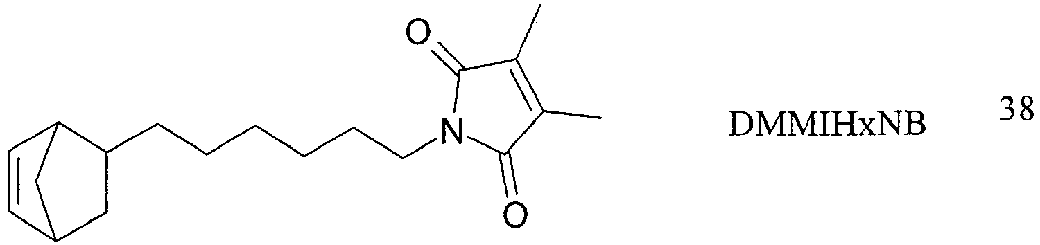
- IJWCNIZYIKMAET-UHFFFAOYSA-N CC(C(N1CCCCCCC(C2)C3C=CC2C3)=O)=C(C)C1=O Chemical compound CC(C(N1CCCCCCC(C2)C3C=CC2C3)=O)=C(C)C1=O IJWCNIZYIKMAET-UHFFFAOYSA-N 0.000 description 1
- FQTWNZNWCJRFEE-UHFFFAOYSA-N Fc(ccc(CC(C1)C2C=CC1C2)c1)c1F Chemical compound Fc(ccc(CC(C1)C2C=CC1C2)c1)c1F FQTWNZNWCJRFEE-UHFFFAOYSA-N 0.000 description 1
- NDBGZVUVINJUAX-UHFFFAOYSA-N O=C(C(CC1)=C2c3c1cccc3)N(CC(C1)C3C=CC1C3)C2=O Chemical compound O=C(C(CC1)=C2c3c1cccc3)N(CC(C1)C3C=CC1C3)C2=O NDBGZVUVINJUAX-UHFFFAOYSA-N 0.000 description 1
- JFHUWIKUXLRRDL-UHFFFAOYSA-N O=C1Oc2cc(OCC(C3)C4C=CC3C4)ccc2C=C1 Chemical compound O=C1Oc2cc(OCC(C3)C4C=CC3C4)ccc2C=C1 JFHUWIKUXLRRDL-UHFFFAOYSA-N 0.000 description 1
Images


Classifications
-
- H—ELECTRICITY
- H10—SEMICONDUCTOR DEVICES; ELECTRIC SOLID-STATE DEVICES NOT OTHERWISE PROVIDED FOR
- H10K—ORGANIC ELECTRIC SOLID-STATE DEVICES
- H10K59/00—Integrated devices, or assemblies of multiple devices, comprising at least one organic light-emitting element covered by group H10K50/00
-
- C—CHEMISTRY; METALLURGY
- C08—ORGANIC MACROMOLECULAR COMPOUNDS; THEIR PREPARATION OR CHEMICAL WORKING-UP; COMPOSITIONS BASED THEREON
- C08F—MACROMOLECULAR COMPOUNDS OBTAINED BY REACTIONS ONLY INVOLVING CARBON-TO-CARBON UNSATURATED BONDS
- C08F232/00—Copolymers of cyclic compounds containing no unsaturated aliphatic radicals in a side chain, and having one or more carbon-to-carbon double bonds in a carbocyclic ring system
- C08F232/08—Copolymers of cyclic compounds containing no unsaturated aliphatic radicals in a side chain, and having one or more carbon-to-carbon double bonds in a carbocyclic ring system having condensed rings
-
- C—CHEMISTRY; METALLURGY
- C08—ORGANIC MACROMOLECULAR COMPOUNDS; THEIR PREPARATION OR CHEMICAL WORKING-UP; COMPOSITIONS BASED THEREON
- C08G—MACROMOLECULAR COMPOUNDS OBTAINED OTHERWISE THAN BY REACTIONS ONLY INVOLVING UNSATURATED CARBON-TO-CARBON BONDS
- C08G61/00—Macromolecular compounds obtained by reactions forming a carbon-to-carbon link in the main chain of the macromolecule
- C08G61/02—Macromolecular compounds containing only carbon atoms in the main chain of the macromolecule, e.g. polyxylylenes
- C08G61/04—Macromolecular compounds containing only carbon atoms in the main chain of the macromolecule, e.g. polyxylylenes only aliphatic carbon atoms
- C08G61/06—Macromolecular compounds containing only carbon atoms in the main chain of the macromolecule, e.g. polyxylylenes only aliphatic carbon atoms prepared by ring-opening of carbocyclic compounds
- C08G61/08—Macromolecular compounds containing only carbon atoms in the main chain of the macromolecule, e.g. polyxylylenes only aliphatic carbon atoms prepared by ring-opening of carbocyclic compounds of carbocyclic compounds containing one or more carbon-to-carbon double bonds in the ring
-
- C—CHEMISTRY; METALLURGY
- C08—ORGANIC MACROMOLECULAR COMPOUNDS; THEIR PREPARATION OR CHEMICAL WORKING-UP; COMPOSITIONS BASED THEREON
- C08L—COMPOSITIONS OF MACROMOLECULAR COMPOUNDS
- C08L45/00—Compositions of homopolymers or copolymers of compounds having no unsaturated aliphatic radicals in side chain, and having one or more carbon-to-carbon double bonds in a carbocyclic or in a heterocyclic ring system; Compositions of derivatives of such polymers
-
- C—CHEMISTRY; METALLURGY
- C08—ORGANIC MACROMOLECULAR COMPOUNDS; THEIR PREPARATION OR CHEMICAL WORKING-UP; COMPOSITIONS BASED THEREON
- C08L—COMPOSITIONS OF MACROMOLECULAR COMPOUNDS
- C08L65/00—Compositions of macromolecular compounds obtained by reactions forming a carbon-to-carbon link in the main chain; Compositions of derivatives of such polymers
-
- H—ELECTRICITY
- H10—SEMICONDUCTOR DEVICES; ELECTRIC SOLID-STATE DEVICES NOT OTHERWISE PROVIDED FOR
- H10K—ORGANIC ELECTRIC SOLID-STATE DEVICES
- H10K10/00—Organic devices specially adapted for rectifying, amplifying, oscillating or switching; Organic capacitors or resistors having potential barriers
- H10K10/40—Organic transistors
- H10K10/46—Field-effect transistors, e.g. organic thin-film transistors [OTFT]
- H10K10/462—Insulated gate field-effect transistors [IGFETs]
- H10K10/464—Lateral top-gate IGFETs comprising only a single gate
-
- H—ELECTRICITY
- H10—SEMICONDUCTOR DEVICES; ELECTRIC SOLID-STATE DEVICES NOT OTHERWISE PROVIDED FOR
- H10K—ORGANIC ELECTRIC SOLID-STATE DEVICES
- H10K10/00—Organic devices specially adapted for rectifying, amplifying, oscillating or switching; Organic capacitors or resistors having potential barriers
- H10K10/40—Organic transistors
- H10K10/46—Field-effect transistors, e.g. organic thin-film transistors [OTFT]
- H10K10/462—Insulated gate field-effect transistors [IGFETs]
- H10K10/466—Lateral bottom-gate IGFETs comprising only a single gate
-
- H—ELECTRICITY
- H10—SEMICONDUCTOR DEVICES; ELECTRIC SOLID-STATE DEVICES NOT OTHERWISE PROVIDED FOR
- H10K—ORGANIC ELECTRIC SOLID-STATE DEVICES
- H10K50/00—Organic light-emitting devices
- H10K50/80—Constructional details
-
- H—ELECTRICITY
- H10—SEMICONDUCTOR DEVICES; ELECTRIC SOLID-STATE DEVICES NOT OTHERWISE PROVIDED FOR
- H10K—ORGANIC ELECTRIC SOLID-STATE DEVICES
- H10K59/00—Integrated devices, or assemblies of multiple devices, comprising at least one organic light-emitting element covered by group H10K50/00
- H10K59/10—OLED displays
- H10K59/12—Active-matrix OLED [AMOLED] displays
- H10K59/122—Pixel-defining structures or layers, e.g. banks
-
- H—ELECTRICITY
- H10—SEMICONDUCTOR DEVICES; ELECTRIC SOLID-STATE DEVICES NOT OTHERWISE PROVIDED FOR
- H10K—ORGANIC ELECTRIC SOLID-STATE DEVICES
- H10K59/00—Integrated devices, or assemblies of multiple devices, comprising at least one organic light-emitting element covered by group H10K50/00
- H10K59/10—OLED displays
- H10K59/17—Passive-matrix OLED displays
- H10K59/173—Passive-matrix OLED displays comprising banks or shadow masks
-
- H—ELECTRICITY
- H10—SEMICONDUCTOR DEVICES; ELECTRIC SOLID-STATE DEVICES NOT OTHERWISE PROVIDED FOR
- H10K—ORGANIC ELECTRIC SOLID-STATE DEVICES
- H10K85/00—Organic materials used in the body or electrodes of devices covered by this subclass
- H10K85/10—Organic polymers or oligomers
-
- H—ELECTRICITY
- H10—SEMICONDUCTOR DEVICES; ELECTRIC SOLID-STATE DEVICES NOT OTHERWISE PROVIDED FOR
- H10K—ORGANIC ELECTRIC SOLID-STATE DEVICES
- H10K85/00—Organic materials used in the body or electrodes of devices covered by this subclass
- H10K85/10—Organic polymers or oligomers
- H10K85/111—Organic polymers or oligomers comprising aromatic, heteroaromatic, or aryl chains, e.g. polyaniline, polyphenylene or polyphenylene vinylene
-
- C—CHEMISTRY; METALLURGY
- C08—ORGANIC MACROMOLECULAR COMPOUNDS; THEIR PREPARATION OR CHEMICAL WORKING-UP; COMPOSITIONS BASED THEREON
- C08G—MACROMOLECULAR COMPOUNDS OBTAINED OTHERWISE THAN BY REACTIONS ONLY INVOLVING UNSATURATED CARBON-TO-CARBON BONDS
- C08G2261/00—Macromolecular compounds obtained by reactions forming a carbon-to-carbon link in the main chain of the macromolecule
- C08G2261/40—Polymerisation processes
- C08G2261/41—Organometallic coupling reactions
- C08G2261/418—Ring opening metathesis polymerisation [ROMP]
-
- Y—GENERAL TAGGING OF NEW TECHNOLOGICAL DEVELOPMENTS; GENERAL TAGGING OF CROSS-SECTIONAL TECHNOLOGIES SPANNING OVER SEVERAL SECTIONS OF THE IPC; TECHNICAL SUBJECTS COVERED BY FORMER USPC CROSS-REFERENCE ART COLLECTIONS [XRACs] AND DIGESTS
- Y02—TECHNOLOGIES OR APPLICATIONS FOR MITIGATION OR ADAPTATION AGAINST CLIMATE CHANGE
- Y02E—REDUCTION OF GREENHOUSE GAS [GHG] EMISSIONS, RELATED TO ENERGY GENERATION, TRANSMISSION OR DISTRIBUTION
- Y02E10/00—Energy generation through renewable energy sources
- Y02E10/50—Photovoltaic [PV] energy
- Y02E10/549—Organic PV cells
Definitions
- halohydrocarbyl as used herein is inclusive of the hydrocarbyl moieties mentioned above but where there is a degree of halogenation that can range from at least one hydrogen atom being replaced by a halogen atom (e.g., a fluoromethyl group) to where all hydrogen atoms on the hydrocarbyl group have been replaced by a halogen atom (e.g., trifluoromethyl or perfluoromethyl), also referred to as perhalogenation.
- a halogen atom e.g., a fluoromethyl group
- heteroatom containing moieties can be referred to as, for example, either "heteroatom-hydrocarbyls" or “heterohydrocarbyls”, including, among others, ethers, epoxies, glycidyl ethers, alcohols, carboxylic acids, esters, maleimides, amines, imines, amides, phenols, amido-phenols, silanes, siloxanes, phosphines, phosphine oxides, phosphinites, phosphonites, phosphites, phosphonates, phosphinates, and phosphates.
- ethers epoxies
- glycidyl ethers alcohols
- carboxylic acids esters
- maleimides amines, imines, amides, phenols, amido-phenols, silanes, siloxanes
- phosphines phosphine oxides
- phosphinites phosphonite
- the repeating units of Formula I are formed from the corresponding norbornene-type monomers of Formula Ia where Z, m and R 1-4 are as defined above:
- one or more of R 1-4 denote a halogenated or perhalogenated aryl or aralkyl group including, but not limited to those of the formula -(CH 2 ) x -C 6 F y H 5-y , and -(CH 2 ) x -C 6 F y H 4-y - p C z F q H 2z+1-q , where x, y, q, and z are independently selected integers from 0 to 5, 0 to 5, 0 to 9, and 1 to 4, respectively, and " p " means "para".
- the crosslinkable group of the crosslinker is preferably selected from a maleimide, a 3-monoalkyl-maleimide, a 3,4-dialkylmaleimide, an epoxy, a vinyl, an acetylene, an indenyl, a cinnamate or a coumarin group, or a group that comprises a substituted or unsubstituted maleimide portion, an epoxide portion, a vinyl portion, an acetylene portion, an indenyl portion,a cinnamate portion or a coumarin portion.
- G 2 is preferably a crosslinkable group selected from a maleimide, a 3-monoalkyl-maleimide, a 3,4-dialkylmaleimide, an epoxy, a vinyl, an acetyl, an indenyl, a cinnamate or a coumarin group, or comprises a substituted or unsubstituted maleimide portion, an epoxide portion, a vinyl portion, an acetyl portion, an indenyl portion, a cinnamate portion or a coumarin portion.
- a crosslinkable group selected from a maleimide, a 3-monoalkyl-maleimide, a 3,4-dialkylmaleimide, an epoxy, a vinyl, an acetyl, an indenyl, a cinnamate or a coumarin group, or comprises a substituted or unsubstituted maleimide portion, an epoxide portion, a vinyl portion, an acetyl
- the polycycloolefinic polymers used in the bank structures in accordance with the present invention can be tailored to overcome the drawbacks that have been observed in previously known bank structure materials, such as limited processability and limited solubility in organic solvents.
- the polycycloolefinic polymers show a good tunability of the polymers' properties like their solubility in organic solvents, and allow a flexible material design that combines both hydrophobicity and UV sensitivity.
- they are processable from unfluorinated, environmentally benign solvents, can be cross-linked by UV curing processes, and can be deposited by standard methods like ink-jet printing or flexo printing
- OFET embodiments in accordance with the present invention preferably employ a gate dielectric layer (3) that consists of a dielectric material ("gate dielectric") having a permittivity ( ⁇ of 3.0 or less (“low k dielectric”), as disclosed in WO 03/052841 .
- ⁇ is in the range of from 1.3 to 3.0, preferably from 1.7, to 3.0 has been found to be appropriate while in other preferred embodiments a range from 2.0 to 3.0 is appropriate.
- a permittivity range of from 2.5 to 3.0 or from 2.0 to 2.6 has been found to be appropriate.
- Exemplary electrode materials include polyaniline, polypyrrole, poly(3,4-ethylenedioxythiophene) (PEDOT) or doped conjugated polymers, further dispersions or pastes of graphite or particles of metal such as Au, Ag, Cu, Al, Ni or their mixtures as well as sputter coated or evaporated metals such as Cu, Cr, Pt/Pd, Ag, Au or metal oxides such as indium tin oxide (ITO) F-doped ITO or Al-doped ZnO.
- Organometallic precursors may also be used and deposited from a liquid phase.
- the binder which is typically a polymer, may comprise either an insulating binder or a semiconducting binder, or mixtures thereof may be referred to herein as the organic binder, the polymeric binder, or simply the binder.
- the organic binder is one in which at least 95% of the atoms, very preferably at least 98% of the atoms, and most preferably all of the atoms are selected from hydrogen, fluorine and carbon atoms.
- a 15% solution of a copolymer of NBC 4 F 9 and DMMIBuNB, ratio of co-monomers 44/56, Mw 83,200, in MAK is spun at 1500rpm creating a film with a thickness of 500 nm.
- Figures 12a and 12b show photomicrographs taken using a UV light source. It can be seen that good film formation is obtained, and the ink is contained within the pixelated structure. It is also observed that the ink does not wet the bank structure material.
Landscapes
- Chemical & Material Sciences (AREA)
- Health & Medical Sciences (AREA)
- Chemical Kinetics & Catalysis (AREA)
- Medicinal Chemistry (AREA)
- Polymers & Plastics (AREA)
- Organic Chemistry (AREA)
- Engineering & Computer Science (AREA)
- Materials Engineering (AREA)
- Microelectronics & Electronic Packaging (AREA)
- Physics & Mathematics (AREA)
- Optics & Photonics (AREA)
- Thin Film Transistor (AREA)
- Addition Polymer Or Copolymer, Post-Treatments, Or Chemical Modifications (AREA)
- Electroluminescent Light Sources (AREA)
- Electrodes Of Semiconductors (AREA)
- Semiconductor Memories (AREA)
- Polyoxymethylene Polymers And Polymers With Carbon-To-Carbon Bonds (AREA)
Description
- The invention generally relates to the use of polycycloolefinic polymers as a structure defining material in organic electronic devices, and more specifically to separators, insulating structures or bank structures of such devices and to organic electronic devices comprising such structures, to processes for preparing such structures and to organic electronic devices encompassing such structures.
- In order to improve the performance of organic electronic (OE) devices, such as organic field effect transistors (OFETs) or organic light emitting diodes (OLEDs), it is desirable to be able to deposit, from a solution, the individual functional layers, for example the semiconductor layer, in a specific, confined place on a substrate.
- Bank structures, and methods of forming them, are known to be used for defining such confined places on a substrate. For example,
US 2007/0023837 A1 ,WO 2008/117395 A1 ,EP 1 933 393 A1 ,GB 2,458,454 A GB 2,462,845 A US 2003/017360 A1 ,US 2007/190673 A1 ,WO 2007/023272 A1 andWO 2009/077738 A1 individually and collectively are representative disclosures of such known structures and methods. However, despite these disclosures, none provide a manufacturing process or material that is compatible with ink-jet printing or photolithography, or that discloses a solution processable material that is useable without harmful reactive or migrating chemicals or methods. - Thus it would be desiraable to provide structure defining materials for use in forming bank structures that are compatible with ink-jet printing or photolithography which are essentially free of the aforementioned harmful reactive or migrating chemicals. Additionally it would be desirable to provide methods of forming such bank structures using methods that are both compatible with ink-jet printing or photolithography and do not require the use of processes such as halocarbon reactive ion etchhing. Still further it would be desirable to provide OE devices manufactured using such desirable structure defining materials and structure forming methods.
- One aim of the present invention is to provide structure defining materials for use in bank structures meeting these requirements. Another aim is to provide structure defining materials which are free of contamination, residual process chemicals, and photocatalyst residues. Another aim is to provide improved methods of manufacturing such bank structures. Another aim is to provide improved OE devices comprising such bank structures. Further aims are immediately evident to the person skilled in the art from the following description.
- The inventors have found these aims can be achieved by providing bank structures, methods of manufacturing them, and structure defining materials comprised therein in accordance with the present invention and as claimed hereinafter. The present inventions more specifically relates to OE devices and methods of manufacturing the same using solution processing methods, and novel structure-defining polymers based on polycycloolefinic polymers for manufacturing the bank structures therein. It was found that the use of polycycloolefinic polymers as structure defining material provides several advantages. These polymers combine the processing from non-fluorinated environmentally benign solvents with the possibility of applying UV curing processes, and can also be coated by standard methods like ink-jet printing or flexo printing. Besides, the processing and curing of these polymers does not require photoactive additives like photocatalysts, so that impurities resulting from the photoreaction of such additives can be avoided in the cured structures.
- The present invention also presents a single layer approach towards bank structures, provides flexibility of the material design towards both hydrophobicity and UV sensitivity, and enables tuning the solubility profile of the structure defining material.
-
WO 03/079458 A1 WO 2008/070774 A1 ,US 2006/020068 A1 andUS 2012/056183 A1 disclose crosslinkable polynorbornenes for use in dielectrics, barrier layers, buffer layers or gate insulators of electronic devices. However, none of these documents discloses or suggests an OFET device with bank structures as claimed in the present application. - The invention relates an organic electronic device as claimed in
claim 1 comprising one or more bank structures, wherein said defined structures comprise a polycycloolefinic polymer. - The organic electronic device is an Organic Field Effect Transistor (OFET), including Organic Thin Film Transistors (OTFT), especially a top gate OFET or bottom gate OFET.
- The invention further relates to a product or an assembly comprising an organic electronic device as described above and below. Such product or assembly is preferably an Integrated Circuit (IC), a Radio Frequency Identification (RFID) tag, a security marking or security device containing an RFID tag, a Flat Panel Display (FPD), a backplane of an FPD, a backlight of an FPD, an electrophotographic device, an electrophotographic recording device, an organic memory device, a sensor, a biosensor or a biochip.
- The invention further relates to a process of preparing an organic electronic device, like a top gate OFET or bottom gate OFET, comprising one or more bank structures as described hereinafter.
- Embodiments of the invention are described below with reference to the following drawings.
-
Figure 1 is a schematic representation of a bottom gate OFET device in accordance with the present invention; -
Figure 2 is a schematic representation of a top gate OFET device in accordance with the present invention; -
Figure 3 is a schematic representation of a bank structure pattern in an OFET device of Example 1, 2 and 4. -
Figure 4 is a schematic representation of a bank structure pattern in an OFET device of Example 3. -
Figure 5 is a transfer curve of a bottom gate OFET device of Example 1. -
Figure 6 is a transfer curve of a bottom gate OFET device of Example 2. -
Figure 7 is a transfer curve of a bottom gate OFET device of Example 3. -
Figure 8 is a transfer curve of a bottom gate OFET device of Comparison Example 1. -
Figure 9 is a transfer curve of a top gate OFET device of Example 4. -
Figure 10 is a transfer curve of a top gate OFET device of Comparison Example 2. -
Figures 11a and 11b are images of photopatterned bank structures used in the preparation of an OLED device of Example 5. -
Figures 12a and 12b show photomicrographs of an OLED ink printed into the photopatterned bank structures in an OLED device of Example 5. -
Figure 13 is an image of an ink-jet patterned bank structure used in the preparation of an OLED device of Example 6. -
Figure 14 is a photomicrograph of an OLED ink printed into the photopatterned bank structures in an OLED device of Example 6. - As used herein, the term Organic Field Effect Transistors (OFET) will be understood to be inclusive of the subclass of such devices known as Organic Thin Film Transistors (OTFTs).
- In addition, it will be understood that the terms "dielectric" and "insulating" are used interchangeably herein. Thus reference to an insulating material or layer is inclusive of a dielectric material or layer and vice versa. Further, as used herein, the term "organic electronic device" will be understood to be inclusive of the term "organic semiconductor device" and the several specific implementations of such devices such as the OFETs as defined above.
- As used herein, the terms "orthogonal" and "orthogonality" will be understood to mean chemical orthogonality. For example, an orthogonal solvent means a solvent which, when used in the deposition of a layer of a material dissolved therein on a previously deposited layer, does not dissolve said previously deposited layer.
- As used herein, the terms "insulating structure(s)" and "bank structure(s)" will be understood to mean a patterned structure, for example a patterned layer, that is provided on an underlying substrate and defines a specific structure, for example a well, on said substrate that can be filled by a functional material like a semiconductor or a dielectric. The patterned structure comprises a structure defining material that is selected such that a surface energy contrast is created between said patterned structure and said substrate. Usually the substrate has a higher surface energy while the patterned structure has a lower surface energy. The substrate is for example a functional layer of an electronic device, like an electrode, a semiconducting layer or a dielectric layer. The insulating or bank structure is used to define more easily the active area of a solution-processed thin film of, for example,. the semiconductor in an electronic device, by using the tendency of the liquid solution to move and stick to the area having higher surface energy, i.e., the substrate. By confining the liquid in a given area, a thin film can be formed as needed in the specific device application. This provides certain benefits, for example in OFETs the confined area of organic semiconductor improves the off-state current. It will be understood that the terms "bank structure(s)" and "insulating structure(s)" are used interchangeably herein. Thus reference to a bank structure is inclusive of an insulating structure.
- As used herein, the term "polymer" will be understood to mean a molecule that encompasses a backbone of one or more distinct types of repeating units (the smallest constitutional unit of the molecule) and is inclusive of the commonly known terms "oligomer", "copolymer", "homopolymer" and the like. Further, it will be understood that the term polymer is inclusive of, in addition to the polymer itself, residues from initiators, catalysts and other elements attendant to the synthesis of such a polymer, where such residues are understood as not being covalently incorporated thereto. Further, such residues and other elements, while normally removed during post polymerization purification processes, are typically mixed or co-mingled with the polymer such that they generally remain with the polymer when it is transferred between vessels or between solvents or dispersion media.
- As used herein, the term "polymer composition" means at least one polymer and one or more other materials added to the at least one polymer to provide, or to modify, specific properties of the polymer composition and or the at least one polymer therein. It will be understood that a polymer composition is a vehicle for carrying the polymer to a substrate to enable the forming of layers or structures thereon. Exemplary materials include, but are not limited to, solvents, antioxidants, photoinitiators, photosensitizers, crosslinking moieties or agents, reactive diluents, acid scavengers, leveling agents and adhesion promoters. Further, it will be understood that a polymer composition may, in addition to the aforementioned exemplary materials, also encompass a blend of two or more polymers.
- As defined herein, the terms "polycycloolefin", "polycyclic olefin", and "norbornene-type" are used interchangeably and refer to addition polymerizable monomers, or the resulting repeating unit, encompassing at least one norbornene moiety such as shown by either Structure A1 or A2, below. The simplest norbornene-type or polycyclic olefin monomer bicyclo[2.2.1]hept-2-ene (A1) is commonly referred to as norbornene.

- However, the term "norbornene-type monomer" or " norbornene-type repeating unit", as used herein, is understood to not only mean norbornene itself but also to refer to any substituted norbornene, or substituted and unsubstituted higher cyclic derivatives thereof, for example of Structures B1 and B2, shown below, wherein m is an integer greater than zero.

- By the substitution of a norbornene-type monomer with a pendant group, the properties of a polymer formed therefrom can be tailored to fulfill the needs of individual applications. The procedures and methods that have been developed to polymerize functionalized norbornene-type monomers exhibit an outstanding flexibility and tolerance to various moieties and groups of the monomers. In addition to polymerization of monomers with a specific pendant group, monomers having a variety of distinct functionalities can be randomly polymerized to form a final material where the types and ratios of monomers used dictate the overall bulk properties of the resulting polymer.
- As used herein, "hydrocarbyl" refers to a radical or group that contains a carbon backbone where each carbon is appropriately substituted with one or more hydrogen atoms. The term "halohydrocarbyl" refers to a hydrocarbyl group where one or more of the hydrogen atoms, but not all, have been replaced by a halogen (F, Cl, Br, or I). The term perhalocarbyl refers to a hydrocarbyl group where each hydrogen has been replaced by a halogen. Non-limiting examples of hydrocarbyls, include, but are not limited to a C1-C25 alkyl, a C2-C24 alkenyl, a C2-C24 alkynyl, a C5-C25 cycloalkyl, a C6-C24 aryl or a C7-C24 aralkyl. Representative alkyl groups include but are not limited to methyl, ethyl, propyl, isopropyl, butyl, isobutyl, sec-butyl, tert-butyl, pentyl, neopentyl, hexyl, heptyl, octyl, nonyl, decyl and dodecyl. Representative alkenyl groups include but are not limited to vinyl, propenyl, butenyl and hexenyl. Representative alkynyl groups include but are not limited to ethynyl, 1-propynyl, 2-propynyl, 1 butynyl, and 2-butynyl. Representative cycloalkyl groups include but are not limited to cyclopentyl, cyclohexyl, and cyclooctyl substituents. Representative aryl groups include but are not limited to phenyl, biphenyl, naphthyl, and anthracenyl. Representative aralkyl groups include but are not limited to benzyl, phenethyl and phenbutyl.
- The term "halohydrocarbyl" as used herein is inclusive of the hydrocarbyl moieties mentioned above but where there is a degree of halogenation that can range from at least one hydrogen atom being replaced by a halogen atom (e.g., a fluoromethyl group) to where all hydrogen atoms on the hydrocarbyl group have been replaced by a halogen atom (e.g., trifluoromethyl or perfluoromethyl), also referred to as perhalogenation. For example, halogenated alkyl groups that can be useful in embodiments of the present invention can be partially or fully halogenated, alkyl groups of the formula CaX2a+1 wherein X is independently a halogen or a hydrogen and a is selected from an integer of 1 to 25. In some embodiments each X is independently selected from hydrogen, chlorine, fluorine bromine and/or iodine. In other embodiments each X is independently either hydrogen or fluorine. Thus, representative halohydrocarbyls and perhalocarbyls are exemplified by the aforementioned exemplary hydrocarbyls where an appropriate number of hydrogen atoms are each replaced with a halogen atom.
- In addition, the definition of the terms "hydrocarbyl", "halohydrocarbyl", and "perhalohydrocarbyl", are inclusive of moieties where one or more of the carbon atoms is replaced by a heteroatom selected independently from O, N, P, or Si. Such heteroatom containing moieties can be referred to as, for example, either "heteroatom-hydrocarbyls" or "heterohydrocarbyls", including, among others, ethers, epoxies, glycidyl ethers, alcohols, carboxylic acids, esters, maleimides, amines, imines, amides, phenols, amido-phenols, silanes, siloxanes, phosphines, phosphine oxides, phosphinites, phosphonites, phosphites, phosphonates, phosphinates, and phosphates.
- Further exemplary hydrocarbyls, halohydrocarbyls, and perhalocarbyls, inclusive of heteroatoms, include, but are not limited to, -(CH2)n-Ar-(CH2)n-C(CF3)2-OH, -(CH2)n-Ar-(CH2)n-OCH2C(CF3)2-OH, -(CH2)n-C(CF3)2-OH, -((CH2)i-O-)k-(CH2)-C(CF3)2-OH, -(CH2)n-C(CF3)(CH3)-OH, -(CH2)n-C(O)NHR*, -(CH2)n-C(O)CI, -(CH2)n-C(O)OR*, -(CH2)n-OR*, -(CH2)n-OC(O)R* and -(CH2)n-C(O)R*, where n independently represents an integer from 0 to 12, i is 2, 3 or 4, k is 1, 2 or 3, Ar is aryl, for example phenyl, and R* independently represents hydrogen, a C1-C11 alkyl, a C1-C11 halogenated or perhalogenated alkyl, a C2-C10 alkenyl, a C2-C10 alkynyl, a C5-C12 cycloalkyl, a C6-C14 aryl, a C6-C14 halogenated or perhalogenated aryl, a C7-C14 aralkyl or a halogenated or perhalogenated C7-C14 aralkyl.
- Exemplary perhalogenated alkyl groups include, but are not limited to, trifluoromethyl, trichloromethyl, -C2F5, -C3F7, -C4F9, C6F13-, -C7F15, and -C11F23. Exemplary halogenated or perhalogenated aryl and aralkyl groups include, but are not limited to, groups having the formula -(CH2)x-C6FyH5-y, and -(CH2)x-C6FyH4-y-pCzFqH2z+1-q, where x, y, q and z are independently selected integers from 0 to 5, 0 to 5, 0 to 9 and 1 to 4, respectively. Specifically, such exemplary halogenated or perhalogenated aryl groups include, but are not limited to, pentachlorophenyl, pentafluorophenyl, pentafluorobenzyl, 4-trifluoromethylbenzyl, pentafluorophenethyl, pentafluorophenpropyl, and pentafluorophenbutyl.
- The polycycloolefinic polymers as used in the bank structures of the present invention are preferably norbornene-type polymers.
- In a preferred embodiment of the present invention, the norbornene-type polymer incorporates two or more distinct types of repeating units.
- In another preferred embodiment of the present invention, the norbornene-type polymer incorporates one or more distinct types of repeating units, where at least one such type of repeating unit encompasses pendant crosslinkable groups or moieties that have some degree of latency. By "latency", it is meant that such groups do not crosslink at ambient conditions or during the initial forming of the polymers, but rather crosslink when such reactions are specifically initiated, for example by actinic radiation or heat. Such latent crosslinkable groups are incorporated into the polymer backbone by, for example, providing one or more norbornene-type monomers encompassing such a pendant crosslinkable group, for example a substituted or unsubstituted maleimide or maleimide containing pendant group, to the polymerization reaction mixture and causing the polymerization thereof. Preferred crosslinkable groups include a group comprising a substituted or unsubstituted maleimide portion, an epoxide portion, a vinyl portion, an acetylene portion, an indenyl portion, a cinnamate portion or a coumarin portion, and more specifically a group selected from a 3-monoalkyl- or 3,4-dialkylmaleimide, epoxy, vinyl, acetylene, cinnamate, indenyl or coumarin group.
- In another preferred embodiment the norbornene-type polymer comprises one or more distinct types of repeating units of Formula I

- The repeating units of Formula I are formed from the corresponding norbornene-type monomers of Formula Ia where Z, m and R1-4 are as defined above:

- In the repeating units and monomers of Formula I and Ia, in a preferred embodiment Z is -CH2- and m is 0, 1 or 2, in another preferred embodiment, Z is -CH2- and m is 0 or 1, and in still another preferred embodiment, Z is -CH2- and m is 0.
- In another preferred embodiment the bank structures comprises a polymer composition which comprises a either a single norbornene-type polymer or a blend of two or more different norbornene-type polymers. Where such polymer composition embodiments encompass a single norbornene-type polymer, such polymer can be a homopolymer, that is to say a polymer encompassing only one type of repeating unit, or a copolymer, that is to say a polymer encompassing two or more distinct types of repeating units. Where such polymer composition embodiments encompass a blend of different polymers, "different" is understood to mean that each of the blended polymers encompasses at least one type of repeating unit, or combination of repeating units, that is distinct from any of the other blended polymers.
- In another preferred embodiment of the invention the polymer composition is a blend of two or more different norbornene-type polymers, wherein each polymer comprises one or more distinct types of repeating units of formula I

- The polymer and polymer composition embodiments of the present invention can advantageously be tailored to provide a distinct set of properties for each of many specific applications. That is to say that different combinations of norbornene-type monomers with several different types of pendant groups can be polymerized to provide norbornene-type polymers having properties that provide for obtaining control over properties such as flexibility, adhesion, dielectric constant, and solubility in organic solvents, among others. For example, varying the length of an alkyl pendant group can allow control of the polymer's modulus and glass transition temperature (Tg). Also, pendant groups selected from maleimide, cinnamate, coumarin, anhydride, alcohol, ester, and epoxy functional groups can be used to promote crosslinking and to modify solubility characteristics. Polar functional groups, epoxy and triethoxysilyl groups can be used to provide adhesion to metals, silicon, and oxides in adjacent device layers. Fluorinated groups, for example, can be used to effectively modify surface energy, dielectric constant and influence the orthogonality of the solution with respect to other materials.
- Thus, in further preferred embodiments of the present invention, in particular for such embodiments where only one of R1-4 is different from H, one or more of R1-4 denote a halogenated or perhalogenated aryl or aralkyl group including, but not limited to those of the formula -(CH2)x-C6FyH5-y, and -(CH2)x-C6FyH4-y-pCzFqH2z+1-q, where x, y, q, and z are independently selected integers from 0 to 5, 0 to 5, 0 to 9, and 1 to 4, respectively, and "p" means "para". Specifically such formulae include, but are not limited to, trifluoromethyl, trichloromethyl, -C2F5, -C3F7, -C4F9, C6F13, -C7F15, -C11F23, pentachlorophenyl, pentafluorophenyl, pentafluorobenzyl, 4-trifluoromethylbenzyl, pentafluorophenylethyl, pentafluorophenpropyl, and pentafluorophenbutyl.
- Further still, some preferred embodiments of the present invention, in particular for such embodiments where only one of R1-4 is different from H , encompass a group that is different from H that is a polar group having a terminal hydroxy, carboxy or oligoethyleneoxy moiety, for example a terminal hydroxyalkyl, alkylcarbonyloxy (for example, acetyl), hydroxy-oligoethyleneoxy, alkyloxy-oligoethyleneoxy or alkylcarbonyloxy-oligoethyleneoxy moiety, where "oligoethyleneoxy" is understood to mean -(CH2CH2O)s- with s being 1, 2 or 3; for example 1-(bicyclo[2.2.1]hept-5-en-2-yl)-2,5,8,11-tetraoxadodecane (NBTODD) where s is 3 and 5-((2-(2-methoxyethoxy)ethoxy)methyl) bicyclo[2.2.1]hept-2-ene (NBTON) where s is 2.
- Further still, in other preferred embodiments of the present invention, in particular for such embodiments where only one of R1-4 is different from H , encompass a group that is different from H that is a group having a pendant silyl group, for example a silyl group represented by -(CH2)n-SiR9 3 where n is an integer from 0 to 12, and each R9 independently represents halogen selected from the group consisting of chlorine, fluorine, bromine and iodine, linear or branched (C1 to C20)alkyl, linear or branched (C1 to C20)alkoxy, substituted or unsubstituted (C6 to C20)aryloxy, linear or branched (C1 to C20)alkyl carbonyloxy; linear or branched (C1 to C20) dialkylamido; substituted or unsubstituted (C6-C20) diarylamido; substituted or unsubstituted (C1-C20)alkylarylamido.
- Yet further still, for such embodiments where only one of R1-4 is different from H and where only one of R5-8 is different from H, preferred embodiments encompass a group that is either a photoreactive or a crosslinkable group. Preferred photoreactive or crosslinkable groups encompass a linking portion L and a functional portion F. Preferably L denotes or comprises a group selected from C1-C12 alkyls, aralkyls, aryls or hetero atom analogs. Further preferably F denotes or comprises one or more of a maleimide, a 3-monoalkyl- or 3,4-dialkylmaleimide, epoxy, vinyl, acetylenic, cinnamate, indenyl or coumarin moiety, which is capable of a crosslinking or 2+2 crosslinking reaction.
- As used herein, the phrase "photoreactive and/or crosslinkable", when used to describe certain pendant groups, will be understood to mean a group that is reactive to actinic radiation and as a result of that reactivity enters into a crosslinking reaction, or a group that is not reactive to actinic radiation but can, in the presence of a crosslinking activator, enter into a crosslinking reaction.
- Preferred repeating units that encompass a pendant photoreactive or crosslinkable group that are representative of Formula I are formed during polymerization from norbornene-type monomers that include, but are not limited to, those selected from the following formulae:



- Further preferred repeating units of Formula I such as described above are derived from one or more norbornene-type monomers represented by the following
structural formulae 1 through 5 below:


- For structural formulae 1-5 above, m is an integer from 0 to 3, A is a connecting, spacer or bridging group selected from (CZ2)n, (CH2)n-(CH=CH)p-(CH2)n, (CH2)n-O-(CH2)n, (CH2)n-C6Q4-(CH2)n, and for
structure 1 additionally selected from (CH2)n-O and C(O)-O; R is selected from H, CZ3, (CZ2)nCZ3, OH, O-(O)CCH3, (CH2CH2O)nCH3, (CH2)n-C6Q5, cinnamate or p-methoxy-cinnamate, coumarin, phenyl-3-indene, epoxide, C≡C-Si(C2H5)3 or C≡C-Si(i-C2H5)3, each n is independently an integer from 0 to 12, p is an integer from 1-6, C6Q4 and C6Q5 denote benzene that is substituted with Q, Q is independently H, F, CH3, CF3 or OCH3, Z is independently H or F, with the proviso that -A-R does not contain an -O-O-(peroxy) linkage, and R" is independently H or CH3. - Further preferred repeating units of Formula I such as described above are formed by one or more norbornene-type monomers that include, but not limited to, those selected from the group consisting of the following formulae:







subformulae formula 20, and b is an integer from 1 to 6. - It will be further noted that while 55 specific examples are provided above, other monomers in accordance with embodiments of the present invention are inclusive of monomers represented by formula Ia where at least one of R1, R2, R3 and R4 are hydrocarbyls, halohydrocarbyls, and perhalocarbyls, inclusive of heteroatoms, that include, -(CH2)n-Ar-(CH2)n-C(CF3)2-OH, -(CH2)n-Ar-(CH2)n-OCH2C(CF3)2-OH, -(CH2)n-C(CF3)2-OH, -((CH2)i-O-)k-(CH2)-C(CF3)2-OH, -(CH2)n-C(CF3)(CH3)-OH, (CH2)n-C(O)NHR*, (CH2)n-C(O)Cl, -(CH2)n-C(O)OR*, (CH2)n-OR*, -(CH2)n-OC(O)R* and -(CH2)n-C(O)R*, where n independently represents an integer from 0 to 12, i is 2, 3 or 4, k is 1, 2 or 3, Ar is aryl, for example phenyl, and R* independently represents hydrogen, a C1-C11 alkyl, a C1-C11 halogenated or perhalogenated alkyl, a C2-C10 alkenyl, a C2-C10 alkynyl, a C5-C12 cycloalkyl, a C6-C14 aryl, a C6-C14 halogenated or perhalogenated aryl, a C7-C14 aralkyl or a halogenated or perhalogenated C7-C14 aralkyl. Exemplary perhalogenated alkyl groups include, but are not limited to, trifluoromethyl, trichloromethyl, -C2F5, -C3F7, -C4F9, -C7F15, and -C11F23. Exemplary halogenated or perhalogenated aryl and aralkyl groups include, but are not limited groups having the formula -(CH2)x-C6FyH5-y, and -(CH2)x-C6FyH4-y-pCzFqH2z+1-q, where x, y, q, and z are independently selected integers from 0 to 5, 0 to 5, 0 to 9, and 1 to 4, respectively. Specifically, such exemplary halogenated or perhalogenated aryl groups include, but are not limited to, pentachlorophenyl, pentafluorophenyl, pentafluorobenzyl, 4-trifluoromethylbenzyl, pentafluorophenylethyl, pentafluorophenpropyl, and pentafluorophenbutyl.
- While Formula I and la, as well as each of the subformulae and generic formulae provided above are depicted without indication of any stereochemistry, it should be noted that generally each of the monomers, unless indicated otherwise, are obtained as diastereomeric mixtures that retain their configuration when converted into repeating units. As the exo- and endo- isomers of such diastereomeric mixtures can have slightly different properties, it should be further understood that preferred embodiments of the present invention are made to take advantage of such differences by using monomers that are either a mixture of isomers that is rich in either the exo- or endo- isomer, or are essentially the pure advantageous isomer.
- Another preferred embodiment of the present invention is directed to polymers of Formula I that comprise repeating units where one of R1-4, for example R1, is a fluorinated or perfluorinated alkyl, aryl or aralkyl group as described above and the others of R1-4 are H. Preferably R1 is selected from one of the above subformulae 15-26 (NBC4F9, NBCH2C6F5, NBC6F5, NBCH2C6H3F2, NBCH2C6H4CF3, NBalkylC6F5, FPCNB, FHCNB, FOCHNB, FPCHNB, C8PFAcNB, PPVENB), and and more preferably from
subformulae 16, 17, 18, 19, 20 or 26 (NBCH2C6F5, NBC6F5, NBCH2C6H3F2, NBCH2C6H4CF3, NBalkylC6F5 or PPVENB). - Another preferred embodiment of the present invention is directed to polymers of Formula I that have repeating units where one of R1-4, for example R1, is a photoreactive or crosslinkable group as described above and the others of R1-4 are H. Preferably R1 is a group as shown in one of the above subformulae 27-50 and more preferably as shown in subformulae 34, 35, 36, 37 and 38 (DMMIMeNB, DMMIEtNB, DMMIPrNB, DMMIBuNB and DMMIHxNB).
- Another preferred embodiment of the present invention is directed to polymers of Formula I that have repeating units where one of R1-4, for example R1, is a polar group having a hydroxy, carboxy, acetoxy or oligoethyleneoxy moiety as described above and the others of R1-4 denote H. Preferably R1 is a group as shown in one of the above subformulae 9-14, and more preferably a group as shown in subformula 9 (MeOAcNB).
- Another preferred embodiment of the present invention is directed to a polymer having a first type of repeating unit selected from fluorinated repeating units as described above and a second type of repeating unit selected from crosslinkable repeating units, also as described above. Preferred polymers of this embodiment include polymers having a first type of repeating unit selected from subformulae 15-26, more preferably 15, 16, 17, 18, 19, 20 and 26 (NBC4F9, NBCH2C6F5, NBC6F5, NBCH2C6H3F2, NBCH2C6H4CF3, NBalkylC6F5, and PPVENB) and a second type of repeating unit selected from subformulae 34, 35, 36, 37 and 38 (DMMIMeNB, DMMIEtNB, DMMIPrNB, DMMIBuNB and DMMIHxNB).
- Another preferred embodiment of the present invention is directed to a polymer having a first type of repeating unit selected from fluorinated repeating units as described above, a second type of repeating unit selected from crosslinkable repeating units, also as described above and a third type of repeating unit selected from polar repeating units, again as described above. Preferred polymers of this embodiment include polymers having a first repeating unit of subformula 9 (MeOAcNB), a second type of repeating unit selected from subformulae 34, 35, 36, 37, or 38 (DMMIMeNB, DMMIEtNB, DMMIPrNB, DMMIBuNB and DMMIHxNB), and a third type of repeating unit selected from subformula 16 (NBCH2C6F5).
- Another preferred embodiment of the present invention is directed to a polymer having more than three different types of repeating units in accordance with Formula I. Another preferred embodiment of the present invention is directed to a polymer blend of a first polymer having a first type of repeating unit in accordance with Formula I, and a second polymer having, at least, a first type of repeating unit and a second type of repeating unit in accordance with Formula I that is distinct from the first type. Alternatively such polymer blends can encompass the aforementioned second polymer mixed with an alternative first polymer having two or more distinct types of repeat units in accordance with Formula I. Further preferably, such polymer blends can encompass the aforementioned alternative first polymer mixed with an alternative second polymer having three distinct types of repeat units in accordance with Formula I.
- Another preferred embodiment of the present invention is directed to a polymer having a first and a second distinct type of repeat units in accordance with Formula I where the ratio of such first and second type of repeat units is from 95:5 to 5:95. In another preferred embodiment the ratio of such first and second type of repeat units is from 80:20 to 20: 80. In still another preferred embodiment the ratio of such first and second type of repeat units is from 60:40 to 40:60. In yet another preferred embodiment the ratio of such first and second type of repeat units is from 55:45 to 45:55.
- Examples of suitable and preferred norbornene monomers, polymers and methods for their synthesis are provided herein and can also be found in
US 5,468,819 ,US 6,538,087 ,US 2006/0020068 A1 ,US 2007/0066775 A1 ,US 2008/0194740 A1 ,PCT/EP2011/004281 US Ser.No.13/223,784 PCT/EP2011/004282 US Ser.No.13/223,884 US 2006/0020068 A1 . - The polymer embodiments of the present invention are formed having a weight average molecular weight (Mw) that is appropriate to their use. Generally, a Mw from 5,000 to 500,000 is found appropriate for some embodiments, while for other embodiments other Mw ranges can be advantageous. For example, in a preferred embodiment, the polymer has a Mw of at least 30,000, while in another preferred embodiment the polymer has a Mw of at least 60,000. In another preferred embodiment, the upper limit of the polymer's Mw is up to 400,000, while in another preferred embodiment the upper limit of the polymer's Mw is up to 250,000. It will be understood that since an appropriate Mw is a function of the desired physical properties in the cured polymer, films, layers or structures derived therefrom, it is a design choice and thus any Mw within the ranges provided above is within the scope of the present invention.
- In a preferred embodiment of the present invention, a crosslinkable or crosslinked polycycloolefinic polymer is used as bank structure material or as a component thereof. It has been found that such a crosslinkable or crosslinked polymer can serve to improve one or more properties selected from structural integrity, durability, mechanical resistivity and solvent resistivity of the gate dielectric layer and the electronic device. Very suitable and preferred crosslinkable polymers are for example those having one or more repeating units of Formula I wherein one or more of R1-4 denotes a crosslinkable group, very preferably units formed by monomers selected from subformulae 27-50.
- For crosslinking, the polymer, generally after deposition thereof, is exposed to electron beam or electromagnetic (actinic) radiation such as X-ray, UV or visible radiation, or heated if it contains thermally crosslinkable groups. For example, actinic radiation may be employed to image the polymer using a wavelength of from 11 nm to 700 nm, such as from 200 to 700 nm. A dose of actinic radiation for exposure is generally from 25 to 15000 mJ/cm2. Suitable radiation sources include mercury, mercury/xenon, mercury/halogen and xenon lamps, argon or xenon laser sources, x-ray. Such exposure to actinic radiation is to cause crosslinking in exposed regions. Although other repeating unit pendant groups that crosslink can be provided, generally such crosslinking is provided by repeating units that encompass a maleimide pendant group, that is to say one of R1 to R4 is a substituted or unsubstituted maleimide moiety. If it is desired to use a light source having a wavelength outside of the photo-absorption band of the maleimide group, a radiation sensitive photosensitizer can be added. If the polymer contains thermally crosslinkable groups, optionally an initiator may be added to initiate the crosslinking reaction, for example in case the crosslinking reaction is not initiated thermally.
- In a preferred embodiment, the bank structures are post exposure baked at a temperature from 70°C to 130°C, for example for a period of from 1 to 10 minutes. Post exposure bake can be used to further promote crosslinking of crosslinkable moieties within exposed portions of the polymer.
- In another preferred embodiment, the crosslinkable polymer composition comprises a stabilizer material or moiety to prevent spontaneous crosslinking and improve shelf life of the polymer composition. Suitable stabilizers are antioxidants such as catechol or phenol derivatives that optionally contain one or more bulky alkyl groups, for example t-butyl groups, in ortho-position to the phenolic OH group.
- In order to improve the processing of the individual device components, including functional layers and bank structures, and the integrity of the electronic device, it is desirable to decrease the time needed for the process while keeping or improving the physical properties of the components being formed. This can be maintained where subsequent components and solvents used in forming such components are orthogonal and thus do not dissolve each other. Where such orthogonality is difficult to obtain, crosslinking, typically UV crosslinking, a first component to make such first component insoluble with respect to the polymer composition of a second component will prevent any influence of the properties of either component on the other component.
- Shortening the time needed for the processing can be done for example by tuning the coating process, while decreasing the time needed for UV crosslinking can be achieved both by chemical adjustment of the polymer or by changes in the process.
- However, chemical modifications of polymers are limited, because the UV sensitivity is related to certain properties of the polymer, and for example changes towards increased UV sensitivity may decrease the solubility. Changing the process, for example by using higher power UV, could increase the possibility of creating an ozone atmosphere and thus cause undesired changes in the surface of the polymer dielectric.
- Therefore, in a preferred embodiment of the present invention the polymer composition comprises one or more crosslinker additives. Such additives comprise two or more functional groups that are capable of reacting with the pendant crosslinkable groups of the polycycloolefinic polymer used to form the bank structure. It will also be understood that the use of such crosslinker additives can also enhance the crosslinking of the aforementioned polymer.
- Crosslinking by exposure to UV radiation is preferred.
- The use of a crosslinker enhances the ability to pattern the bank structures through the use of an imagewise exposure to an appropriate wavelength and dose of UV radiation.
- The crosslinkable group of the crosslinker is preferably selected from a maleimide, a 3-monoalkyl-maleimide, a 3,4-dialkylmaleimide, an epoxy, a vinyl, an acetylene, an indenyl, a cinnamate or a coumarin group, or a group that comprises a substituted or unsubstituted maleimide portion, an epoxide portion, a vinyl portion, an acetylene portion, an indenyl portion,a cinnamate portion or a coumarin portion.
- Very preferably the crosslinker is selected of formula III1 or III2
P-A"X'-A"-P III1
H4-cC(A"-P)c III2
wherein X' is O, S, NH or a single bond, A" is a single bond or a connecting, spacer or bridging group, which is selected from (CZ2)n, - (CH2)n-(CH=CH)p-(CH2)n, (CH2)n-O-(CH2)n, (CH2)n-C6Q10-(CH2)n, and C(O), where each n is independently an integer from 0 to 12, p is an integer from 1-6, Z is independently H or F, C6Q10 is cyclohexyl that is substituted with Q, Q is independently H, F, CH3, CF3, or OCH3, P is a crosslinkable group, and c is 2, 3, or 4, and where in formula III1 at least one of X' and the two groups A" is not a single bond.
- P is preferably selected from a maleimide, a 3-monoalkyl-maleimide, a 3,4-dialkylmaleimide, an epoxy, a vinyl, an acetylene, an indenyl, a cinnamate or a coumarin group, or comprises a substituted or unsubstituted maleimide portion, an epoxide portion, a vinyl portion, an acetylene portion, an indenyl portion, a cinnamate portion or a coumarin portion.
- Suitable and preferred compounds of formula III1 are selected from formula C1:

- The spacer group A" preferably denotes linear C1 to C30 alkylene or branched C3 to C30 alkylene or cyclic C5 to C30 alkylene, each of which is unsubstituted or mono- or polysubstituted by F, Cl, Br, I or CN, wherein optionally one or more non-adjacent CH2 groups are replaced, in each case independently from one another, by -O-, -S-, -NH-, -NR18-, -SiR18R19-, -C(O)-, -C(O)O-, -OC(O)-, -OC(O)-O-, -S-C(O)-, -C(O)-S-, -CH=CH- or -C≡C- in such a manner that O and/or S atoms are not linked directly to one another , R18 and R19 are independently of each other H , methyl, ethyl or a C3 to C12 linear or branched alkyl group.
- Preferred groups A" are -(CH2)r-, -(CH2CH2O)s -CH2CH2-, -CH2CH2-S-CH2CH2- or -CH2CH2-NH-CH2CH2- or -(SiR18R19-O)r-, with r being an integer from 2 to 12, s being 1, 2 or 3 and R18 and R19 having the meanings given above.
- Further preferred groups A" are selected from methylene, ethylene, propylene, butylene, pentylene, hexylene, heptylene, octylene, nonylene, decylene, undecylene, dodecylene, octadecylene, ethyleneoxyethylene, methyleneoxybutylene, ethylene-thioethylene, ethylene-N-methyl-iminoethylene, 1-methylalkylene, ethenylene, propenylene and butenylene.
- The synthesis of crosslinkers like those of formula C1 is disclosed for example in
US 3,622,321 . - In another preferred embodiment the polymer composition comprises a crosslinkable polycycloolefinic polymer and a reactive adhesion promoter. The reactive adhesion promoter comprises a first functional group which is a surface-active group that is capable of interactions, for example chemical bonding, with the substrate on which the bank structures are provided, and a second functional group that is capable of interactions, either with or without forming a chemical bond, with the the polycycloolefinic polymer, for example by crosslinking with a pendant crosslinkable group in the polycycloolefinic polymer. The adhesion promoter may be used especially if a photolithography process is employed when providing the bank structures or further functional layers.
- Preferably the adhesion promoter is a compound of formula IV
G1-A"-G2 IV
wherein G1 is a surface-active group, preferably a silane or silazane group, A" is a single bond or a connecting, spacer or bridging group, preferably as defined in formula III1 above, and G2 is a crosslinkable group, preferably as defined in formula III1 above, or G2 is a non-reactive compatibilizing group for the polycycloolefinic polymer. As used herein, the term "compatibilizing" will be understood to mean an interfacial agent or group that facilitates the formation of uniform blends of normally immiscible polymers. For example, if the polycycloolefinic polymer comprises a halogenated or perhalogenated portion, like for example in monomers 15 to 26, the compatibilizing group G2 may be selected from a halogenated or perhalogenated alkyl, aryl or aralkyl group.. - G1 is preferably a group of the formula -SiR12R13R14, or a group of the formula - NH-SiR12R13R14, wherein R12, R13 and R14 are each independently selected from halogen, silazane, C1-C12-alkoxy, C1-C12-alkylamino, optionally substituted C5-C20-aryloxy and optionally substituted C2-C20-heteroaryloxy, and wherein one or two of R12, R13 and R14 may also denote C1-C12-alkyl, optionally substituted C5-C20-aryl or optionally substituted C2-C20-heteroaryl.
- G2 is preferably a crosslinkable group selected from a maleimide, a 3-monoalkyl-maleimide, a 3,4-dialkylmaleimide, an epoxy, a vinyl, an acetyl, an indenyl, a cinnamate or a coumarin group, or comprises a substituted or unsubstituted maleimide portion, an epoxide portion, a vinyl portion, an acetyl portion, an indenyl portion, a cinnamate portion or a coumarin portion.
- In another preferred embodiment, G2 is a non-reactive, compatibilizing group selected from a C1-C11 halogenated or perhalogenated alkyl, a C6-C14 halogenated or perhalogenated aryl, or a halogenated or perhalogenated C7-C14 aralkyl, more preferably from a C1-C11 alkyl, a C6-C14 aryl or a C7-C14 aralkyl each of which is fluorinated or perfluorinated, most preferably from -C4F9, -(CH2)b-C6F5, -CH2C6F2, -CH2-C2F5, -CH2CH2-C4F9, -CH2-(CF2)3-CF2H, -CH2CF2CF2H, -C7F15 or CF2CFHOC3F7, wherein b is an integer from 1 to 6.
- A" is preferably selected from (CZ2)n, (CH2)n-(CH=CH)p-(CH2)n, (CH2)n-O, (CH2)n-O-(CH2)n, (CH2)n-C6Q4-(CH2)n, (CH2)n-C6Q10-(CH2)n and C(O)-O, where each n is independently an integer from 0 to 12, p is an integer from 1-6, Z is independently H or F, C6Q4 is phenyl that is substituted with Q, C6Q10 is cyclohexyl that is substituted with Q, Q is independently H, F, CH3, CF3 or OCH3.
- Suitable and preferred compounds of formula IV are selected from formula A1:

- The aforementioned polymers and polymer compositions are used for forming bank structures in an organic electronic device. The bank structures of the present invention can be used in a large variety of organic electronic OE devices, especially in OFETs and OLEDs, where they are typically located around the electrodes (in OFETs) or on the electrode (in OLEDs).
- The bank structures comprising polycycloolefinic polymers allow for time-, cost- and material-effective production of OE devices, especially OFETs and OLEDs, employing organic semiconductor (OSC) materials and organic dielectric materials on a large scale.
- Advantageously the bank structures of the present invention can be applied as single layer structures. Thus, in a preferred embodiment in accordance with the present invention the bank structures are formed as single layers comprising a polycycloolefinic polymer or a polycycloolefinic polymer blend as described above and below.
- Further advantageously, the polycycloolefinic polymers used in the bank structures in accordance with the present invention can be tailored to overcome the drawbacks that have been observed in previously known bank structure materials, such as limited processability and limited solubility in organic solvents. Thus, the polycycloolefinic polymers show a good tunability of the polymers' properties like their solubility in organic solvents, and allow a flexible material design that combines both hydrophobicity and UV sensitivity. In particular they are processable from unfluorinated, environmentally benign solvents, can be cross-linked by UV curing processes, and can be deposited by standard methods like ink-jet printing or flexo printing
- Thus, in a preferred embodiment in accordance with the present invention the bank structures comprise a polycycloolefinic polymer that comprises a hydrophobic part represented by a fluorinated group and a UV sensitive part represented by a pendant cross-linkable group.
- The bank structures in accordance with the present invention can be provided by additive processing, for example by printing the bank structures from a polymer solution using printing technologies like ink-jet printing, flexographic printing or gravure printing, followed by solvent removal and optionally curing the polymer for example by UV exposure.
- Alternatively the bank structures in accordance with the present invention can be provided by subtractive processing, for example by photolithography-type processing. For example, after spincoating and drying the coated material is exposed to UV radiation like a negative type resist, and is then developed with a solvent to obtain a patterned structure, which can then be further cured by UV exposure to increase the crosslinking.
- In the present invention, the bank structures comprising the polycycloolefinic polymer are provided such that they are overlying the source and drain electrodes in an OFET, and define a well or a pattern of wells in which a functional layer which is an organic semiconducting layer is deposited, so that the bank structures are contacting said electrodes and said functional layer. For example in an OFET comprising source and drain electrodes which are spaced apart to define a channel region located therebetween, the bank structures are deposited overlying the source and drain electrodes, and are patterned such that they define a well that extends over the channel region. An organic semiconducting layer is provided in the channel region, so that the bank structures contact the source and drain electrodes and the organic semiconducting layer.
- A preferred embodiment in accordance with the present invention relates to a process of providing bank structures comprising the following steps: A solution of the bank structure material is spin-coated or otherwise deposited onto a substrate forming a thin film. The thin film is then exposed to UV radiation through a photomask using a mask-aligner. The thin film is then developed to leave a pattern of the exposed bank structure material, washed with organic solvent to remove uncured material, and dried. The bank structure material is then flood-illuminated by UV radiation.
- Another preferred embodiment in accordance with the present invention relates to an organic electronic device comprising, or being obtained through the use of, a polycycloolefinic polymer or a polymer composition as described above and below, which is an organic field effect transistor (OFET) or organic thin film transistor (OTFT), which can be top gate or bottom gate transistors. For example, bottom gate and top gate transistors made through the use of a polymer or polymer composition in accordance with the present invention are depicted schematically in
Figures 1 and 2 . - Turning now to
Figure 1 , a schematic and simplified representation of a bottom gate OFET device in accordance with a preferred embodiment of the present invention is provided. Such OFET device includes a substrate (1), a gate electrode (2), a dielectric layer (3) serving as gate insulator, source and drain electrodes (4) that are spaced apart with a channel region (7) located therebetween, first and second bank structures (5a, 5b) that are patterned such that they define a well (8) that extends over the channel region (7), and an OSC layer (6) provided in the channel region (7), wherein the bank structures (5a, 5b) are derived from a polycycloolefinic polymer or a polymer composition as described above and below. - Another embodiment of the present invention relates to a process for preparing a bottom gate OFET device, for example as illustrated in
Figure 1 , by - a) forming gate electrode (2) on a substrate (1) as depicted,
- b) depositing a layer of dielectric material (3) on the gate electrode (2),
- c) forming source and drain electrodes (4) on the dielectric layer (3) such that they are spaced apart with a channel region (7) located therebetween,
- d) forming bank structures (5a, 5b) by depositing a bank structure material comprising a polycycloolefinic polymer, or comprising a polymer composition comprising a polycycloolefinic polymer, on the source and drain electrodes (4), thereby defining a well (8) that extends over the channel region (7),
- e) depositing a layer of semiconductor material (6) in the well (8) formed by the bank structures (5a, 5b) and onto the source and drain electrodes (4).
- Turning now to
Figure 2 , a schematic and simplified representation of a top gate OFET device in accordance with another preferred embodiment of the present invention is provided. Such OFET device includes a substrate (1), source and drain electrodes (4) that are spaced apart with a channel region (not shown) located therebetween, first and second bank structures (5a, 5b) that are patterned such that they define a well (8) that extends over the channel region, an OSC layer (6) provided in the channel region (7), a dielectric layer (3) serving as gate insulator, and gate electrode (2), wherein the bank structures (5a, 5b) are derived from a polycycloolefinic polymer or a polymer composition as described above and below. - Another embodiment of the present invention relates to a process for preparing a top gate OFET device, for example as illustrated in
Figure 2 , by - a) forming source and drain electrodes (4) on a substrate (1) such that they are spaced apart with a channel region located therebetween,
- b) forming bank structures (5a, 5b) by depositing a bank structure material comprising a polycycloolefinic polymer or a polymer composition comprising a polycycloolefinic polymer on the source and drain electrodes (4), thereby defining a well (8) that extends over the channel region,
- c) depositing a layer of semiconductor material (6) in the well (8) formed by the bank structures (5a, 5b) and onto the source and drain electrodes (4),
- d) depositing a layer of dielectric material (3) on the semiconductor layer (6),
- e) forming gate electrode (2) on the dielectric layer (3).
- The electrodes (2, 4) are for example applied onto the substrate or the dielectric layer (3) by a sputtering process, and can be patterned by etching and/or lithographic patterning. The bank structures (5a, 5b) can be applied in the desired shape by solution processing, e.g. in a printing process, drying and optional curing, or they can be applied and patterned into the desired shape by a lithographic process. The OSC layer (6) and dielectric layer (3) can be applied by a coating or printing process.
- The solvent used for depositing the polycycloolefinic polymer is removed before depositing the organic semiconductor on or between the bank structures or, if a patterning step is included, before said patterning of the bank structures.
- In preferred embodiments in accordance with the present invention, deposition and/or forming of the layers and structures of the OFET are performed using solution processing techniques where such techniques are possible. For example a formulation or composition of a material, typically a solution encompassing one or more organic solvents, can be deposited or formed using preferred techniques that include, but are not limited to, dip coating, slot-die coating spin coating, ink jet printing, letter-press printing, screen printing, doctor blade coating, roller printing, reverse-roller printing, offset lithography printing, flexographic printing, web printing, spray coating, brush coating, or pad printing, followed by the evaporation of the solvent employed to form such a solution. For example, an organic semiconductor material, a bank structure material and an organic dielectric material can each be deposited or formed by spin coating, flexographic printing, and inkjet printing techniques in an order appropriate to the device being formed.
- In a preferred embodiment in accordance with the present invention the polymer composition comprises, in addition to one or more polycycloolefinic polymers, a casting or printing solvent, and optionally one or more additives selected from crosslinking agents, adhesion promoters, reactive solvents, stabilizers, UV sensitizers, and thermal sensitizers.
- The solvents are preferably selected from, but not limited to, organic ketones such as methyl ethyl ketone (MEK), methyl n-amyl ketone (2-heptanone, MAK), decanone, 3-decanone, cyclohexanone and, ethers such as butylphenyl ether, 4-methylanisole and aromatic hydrocarbons such as cyclohexylbenzene, or mixtures thereof. Preferably, the concentration of the bank structure material in the solvent is from 1 to 30 wt. %, although other concentrations can also be appropriate. Organic ketone solvents with a high boiling point have been found to be especially suitable and preferred solvents where inkjet and flexographic printing techniques are employed.
- OFET embodiments in accordance with the present invention preferably employ a gate dielectric layer (3) that consists of a dielectric material ("gate dielectric") having a permittivity (ε of 3.0 or less ("low k dielectric"), as disclosed in
WO 03/052841 - In preferred OFET embodiments in accordance with the present invention that employ a low k gate dielectric material, as described above, for the gate dielectric layer such material is typically an organic fluoropolymer. Suitable fluoropolymers include, for example, highly soluble perfluoropolymers like those from the commercially available CYTOP™ series (Asahi Glass), Teflon AF® series (DuPont) or Hyflon AD® series (from Solvay). CYTOP polymers are described in "Modern Fluoroplastics", edited by John Scheris, John Wiley&Sons Ltd., 1997, Chapter: "Perfluoropolymers Obtained by Cyclopolymerisation" by N. Sugiyama, pages 541ff. Teflon AF is described in "Modern Fluoroplastics", edited by John Scheris, John Wiley&Sons Ltd., 1997, Chapter: "Teflon AF amorphous fluoropolymers" by P. R. Resnick, pages 397ff. Hyflon AD is described in "High Performance Perfluoropolymer Films and Membranes" V. Arcella et. al., Ann. N.Y. Acad. Sci. 984, pages 226-244 (2003).
- The other components or functional layers of the electronic device, like the substrate, the gate and source and drain electrodes, can be selected from standard materials, and can be manufactured and applied to the device by standard methods. Suitable materials and manufacturing methods for these components and layers are known to a person skilled in the art and are described in the literature. Exemplary deposition methods include the liquid coating methods previously described as well as chemical vapor deposition (CVD) or physical vapor deposition methodologies.
- Generally the thickness of a functional layer, for example a gate dielectric or semiconductor layer, in some preferred electronic device embodiments according to the present invention is from 0.001 (in case of a monolayer) to 10 µm; In other preferred embodiments such thickness ranges from 0.001 to 1 µm, and in still other preferred embodiments from 5 nm to 500 nm, although other thicknesses or ranges of thickness are contemplated and thus are within the scope of the present invention.
- Various substrates may be used for the fabrication of the electronic device embodiments of the present invention. For example glass or polymeric materials are most often used. Preferred polymeric materials include, but are not limited to, alkyd resins, allyl esters, benzocyclobutenes, butadienestyrene, cellulose, cellulose acetate, epoxide, epoxy polymers, ethylene-chlorotrifluoro ethylene copolymers, ethylene-tetra-fluoroethylene copolymers, fiber glass enhanced plastic, fluorocarbon polymers, hexafluoropropylenevinylidene-fluoride copolymer, high density polyethylene, parylene, polyamide, polyimide, polyaramid, polydimethylsiloxane, polyethersulphone, poly-ethylene, polyethylenenaphthalate, polyethyleneterephthalate, polyketone, polymethylmethacrylate, polypropylene, polystyrene, polysulphone, polytetrafluoroethylene, polyurethanes, polyvinylchloride, polycycloolefin, silicone rubbers, and silicones, where polyethyleneterephthalate, polyimide, polycycloolefin and polyethylenenaphthalate materials have been found most appropriate. Additionally, for some embodiments of the present invention the substrate can be any suitable material, for example plastic, metal or glass material coated with one or more of the above listed materials. It will be understood that in forming such a substrate, methods such as extruding, stretching, rubbing or photochemical techniques can be employed to provide a homogeneous surface for device fabrication as well as to provide pre-alignment of an organic semiconductor material in order to enhance carrier mobility therein.
- The gate, source and drain electrodes of the OFET device embodiments in accordance with the present invention can be deposited or formed by liquid coating, such as spray-, dip-, web- or spin-coating, or by vacuum deposition methods including but not limited to physical vapor deposition (PVD), chemical vapor deposition (CVD) or thermal evaporation methods. Suitable electrode materials and deposition methods are known to the person skilled in the art. Suitable electrode materials include, without limitation, inorganic or organic materials, or composites of the two. Exemplary electrode materials include polyaniline, polypyrrole, poly(3,4-ethylenedioxythiophene) (PEDOT) or doped conjugated polymers, further dispersions or pastes of graphite or particles of metal such as Au, Ag, Cu, Al, Ni or their mixtures as well as sputter coated or evaporated metals such as Cu, Cr, Pt/Pd, Ag, Au or metal oxides such as indium tin oxide (ITO) F-doped ITO or Al-doped ZnO. Organometallic precursors may also be used and deposited from a liquid phase.
- The organic semiconductor (OSC) layer can be an n- or p- type OSC, which can be deposited by PVD, CVD or solution deposition methods. Effective OSCs exhibit a FET mobility of greater than 1x10⁻⁵ cm2V-1s-1.
- OSC embodiments in accordance with the present invention are OFETs where the OSC is used as the active channel material. OSCs for such embodiments can be deposited by any of the previously discussed deposition methods, but as they are generally deposited or formed as blanket layers, solvent coated methods such as spray-, dip-, web- or spin-coating, or printing methods such as ink-jet printing, flexo printing or gravure printing, are typically employed to allow for ambient temperature processing. However, OSCs can be deposited by any liquid coating technique, for example ink-jet deposition or via PVD or CVD techniques.
- For some preferred OFET embodiments, the semiconducting layer that is formed can be a composite of two or more of the same or different types of semiconductors. For example, a p-type OSC material may, for example, be mixed with an n-type material to achieve a doping effect of the layer. In some preferred embodiments of the invention, multilayer semiconductor layers are used. For example an intrinsic semiconductor layer can be deposited near the gate dielectric interface and a highly doped region can additionally be coated adjacent such an intrinsic layer.
- The OSC material employed for electronic device embodiments in accordance with the present invention can be any conjugated molecule, for example an aromatic molecule containing preferably two or more aromatic rings, very preferably at least three aromatic rings. In some preferred embodiments of the present invention, the OSC contains aromatic rings selected from 5-, 6- or 7-membered aromatic rings, while in other preferred embodiments the OSC contains aromatic rings selected from 5- or 6-membered aromatic rings. The OSC material may be a monomer, oligomer or polymer, including mixtures, dispersions and blends of one or more of monomers, oligomers or polymers.
- Each of the aromatic rings of the OSC optionally contains one or more hetero atoms selected from Se, Te, P, Si, B, As, N, O or S, generally from N, O or S. Further, the aromatic rings may be optionally substituted with alkyl, alkoxy, polyalkoxy, thioalkyl, acyl, aryl or substituted aryl groups, halogen, where fluorine, cyano, nitro or an optionally substituted secondary or tertiary alkylamine or arylamine represented by -N(R15)(R16), where R15 and R16 are each independently H, an optionally substituted alkyl or an optionally substituted aryl, alkoxy or polyalkoxy groups are typically employed. Further, where R15 and R16 is alkyl or aryl these may be optionally fluorinated.
- The aforementioned aromatic rings can be fused rings or linked with a conjugated linking group such as -C(T1)=C(T2)-, -C=C-, -N(R"')-' -N=N-, (R'")=N-, -N=C(R"')-, where T1 and T2 each independently represent H, Cl, F, -C≡N or lower alkyl groups such as C1-4 alkyl groups; R"' represents H, optionally substituted alkyl or optionally substituted aryl. Further, where R'" is alkyl or aryl it can be fluorinated.
- In some preferred OE device embodiments of the present invention, OSC materials that can be used include compounds, oligomers and derivatives of compounds selected from the group consisting of conjugated hydrocarbon polymers such as polyacene, polyphenylene, poly(phenylene vinylene), polyfluorene including oligomers of those conjugated hydrocarbon polymers; condensed aromatic hydrocarbons, such as, tetracene, chrysene, pentacene, pyrene, perylene, coronene, or soluble, substituted derivatives of these; oligomeric para substituted phenylenes such as p-quaterphenyl (p-4P), p-quinquephenyl (p-5P), p-sexiphenyl (p-6P), or soluble substituted derivatives of these; conjugated heterocyclic polymers such as poly(3-substituted thiophene), poly(3,4-bisubstituted thiophene), optionally substituted polythieno[2,3-b]thiophene, optionally substituted polythieno[3,2-b]thiophene, poly(3-substituted selenophene), polybenzothiophene, polyisothianaphthene, poly(N-substituted pyrrole), poly(3-substituted pyrrole), poly(3,4-bisubstituted pyrrole), polyfuran, polypyridine, poly-1,3,4-oxadiazoles, poly(N-substituted aniline), poly(2-substituted aniline), poly(3-substituted aniline), poly(2,3-bisubstituted aniline), polyazulene, polypyrene; pyrazoline compounds; polyselenophene; polybenzofuran; polyindole; polypyridazine; benzidine compounds; stilbene compounds; triazines; substituted metallo- or metal-free porphines, phthalocyanines, fluorophthalocyanines, naphthalocyanines or fluoronaphthalocyanines; C60 and C70 fullerenes; N,N'-dialkyl, substituted dialkyl, diaryl or substituted diaryl-1,4,5,8-naphthalenetetracarboxylic diimide and fluoro derivatives; N,N'-dialkyl, substituted dialkyl, diaryl or substituted diaryl 3,4,9,10-perylenetetracarboxylicdiimide; bathophenanthroline; diphenoquinones; 1,3,4-oxadiazoles; 11,11,12,12-tetracyanonaptho-2,6-quinodimethane; α,α'-bis(dithieno[3,2-b2',3'-d]thiophene); 2,8-dialkyl, substituted dialkyl, diaryl or substituted diaryl anthradithiophene; 2,2'-bibenzo[1,2-b:4,5-b']dithiophene. Where a liquid deposition technique of the OSC is desired, compounds from the above list and derivatives thereof are limited to those that are soluble in an appropriate solvent or mixture of appropriate solvents.
- Further, in some preferred embodiments in accordance with the present invention, the OSC materials are polymers or copolymers that encompass one or more repeating units selected from thiophene-2,5-diyl, 3-substituted thiophene-2,5-diyl, optionally substituted thieno[2,3-b]thiophene-2,5-diyl, optionally substituted thieno[3,2-b]thiophene-2,5-diyl, selenophene-2,5-diyl, or 3-substituted selenophene-2,5-diyl.
- Further preferred p-type OSCs are copolymers comprising electron acceptor and electron donor units. Preferred copolymers of this preferred embodiment are for example copolymers comprising one or more benzo[1,2-b:4,5-b']dithiophene-2,5-diyl units that are preferably 4,8-disubstituted by one or more groups R as defined above, and further comprising one or more aryl or heteroaryl units selected from Group A and Group B, preferably comprising at least one unit of Group A and at least one unit of Group B, wherein Group A consists of aryl or heteroaryl groups having electron donor properties and Group B consists of aryl or heteroaryl groups having electron acceptor properties, and preferably
- Group A consists of selenophene-2,5-diyl, thiophene-2,5-diyl, thieno[3,2-b]thiophene-2,5-diyl, thieno[2,3-b]thiophene-2,5-diyl, selenopheno[3,2-b]selenophene-2,5-diyl, selenopheno[2,3-b]selenophene-2,5-diyl, selenopheno[3,2-b]thiophene-2,5-diyl, selenopheno[2,3-b]thiophene-2,5-diyl, benzo[1,2-b:4,5-b']dithiophene-2,6-diyl, 2,2-dithiophene, 2,2-diselenophene, dithieno[3,2-b:2',3'-d]silole-5,5-diyl, 4H-cyclopenta[2,1-b:3,4-b']dithiophene-2,6-diyl, 2,7-di-thien-2-yl-carbazole, 2,7-di-thien-2-yl-fluorene, indaceno[1,2-b:5,6-b']dithiophene-2,7-diyl, benzo[1",2":4,5;4",5":4',5']bis(silolo[3,2-b:3',2'-b']thiophene)-2,7-diyl, 2,7-di-thien-2-yl-indaceno[1,2-b:5,6-b']dithiophene, 2,7-dithien-2-yl-benzo[1",2":4,5;4",5":4',5']bis(silolo[3,2-b:3',2'-b']thiophene)-2,7-diyl, and 2,7-di-thien-2-yl-phenanthro[1,10,9,8-c,d,e,f,g]carbazole, all of which are optionally substituted by one or more, preferably one or two groups R as defined above, and
- Group B consists of benzo[2,1,3]thiadiazole-4,7-diyl, 5,6-dialkyl-benzo[2,1,3]thiadiazole-4,7-diyl, 5,6-dialkoxybenzo[2,1,3]thiadiazole-4,7-diyl, benzo[2,1,3]selenadiazole-4,7-diyl, 5,6-dialkoxy-benzo[2,1,3]selenadiazole-4,7-diyl, benzo[1,2,5]thiadiazole-4,7,diyl, benzo[1,2,5]selenadiazole-4,7,diyl, benzo[2,1,3]oxadiazole-4,7-diyl, 5,6-dialkoxybenzo[2,1,3]oxadiazole-4,7-diyl, 2H-benzotriazole-4,7-diyl, 2,3-dicyano-1,4-phenylene, 2,5-dicyano,1,4-phenylene, 2,3-difluro-1,4-phenylene, 2,5-difluoro-1,4-phenylene, 2,3,5,6-tetrafluoro-1,4-phenylene, 3,4-difluorothiophene-2,5-diyl, thieno[3,4-b]pyrazine-2,5-diyl, quinoxaline-5,8-diyl, thieno[3,4-b]thiophene-4,6-diyl, thieno[3,4-b]thiophene-6,4-diyl, and 3,6- pyrrolo[3,4-c]pyrrole-1,4-dione, all of which are optionally substituted by one or more, preferably one or two groups R as defined above.
- In other preferred embodiments of the present invention, the OSC materials are substituted oligoacenes such as pentacene, tetracene or anthracene, or heterocyclic derivatives thereof. Bis(trialkylsilylethynyl) oligoacenes or bis(trialkylsilylethynyl) heteroacenes, as disclosed for example in
US 6,690,029 orWO 2005/055248 A1 orUS 7,385,221 , are also useful. - Where appropriate and needed to adjust the rheological properties as described for example in
WO 2005/055248 A1 , some embodiments of the present invention employ OSC compositions that include one or more organic binders. - The binder, which is typically a polymer, may comprise either an insulating binder or a semiconducting binder, or mixtures thereof may be referred to herein as the organic binder, the polymeric binder, or simply the binder.
- Preferred binders according to the present invention are materials of low permittivity, that is, those having a permittivity ε of 3.3 or less. The organic binder preferably has a permittivity ε of 3.0 or less, more preferably 2.9 or less. Preferably the organic binder has a permittivity ε at of 1.7 or more. It is especially preferred that the permittivity of the binder is in the range from 2.0 to 2.9. Whilst not wishing to be bound by any particular theory it is believed that the use of binders with a permittivity ε of greater than 3.3, may lead to a reduction in the OSC layer mobility in an electronic device, for example an OFET. In addition, high permittivity binders could also result in increased current hysteresis of the device, which is undesirable.
- Examples of a suitable organic binders include polystyrene, or polymers or copolymers of styrene and α-methyl styrene, or copolymers including styrene, α-methylstyrene and butadiene may suitably be used. Further examples of suitable binders are disclosed for example in
US 2007/0102696 A1 . - In one type of preferred embodiment, the organic binder is one in which at least 95% of the atoms, very preferably at least 98% of the atoms, and most preferably all of the atoms are selected from hydrogen, fluorine and carbon atoms.
- The binder is preferably capable of forming a film, more preferably a flexible film.
- The binder can also be selected from crosslinkable binders such as acrylates, epoxies, vinylethers, and thiolenes, preferably having a sufficiently low permittivity, very preferably of 3.3 or less. The binder can also be mesogenic or liquid crystalline.
- In another preferred embodiment the binder is a semiconducting binder, which contains conjugated bonds, especially conjugated double bonds and/or aromatic rings. Suitable and preferred binders are for example polytriarylamines as disclosed for example in
US 6,630,566 . - The proportions of binder to OSC is typically 20:1 to 1:20 by weight, preferably 10:1 to 1:10 more preferably 5:1 to 1:5, still more preferably 3:1 to 1:3 further preferably 2:1 to 1:2 and especially 1:1. Dilution of the compound of formula I in the binder has been found to have little or no detrimental effect on the charge mobility, in contrast to what would have been expected from the prior art.
- Unless the context clearly indicates otherwise, as used herein plural forms of the terms herein are to be construed as including the singular form and vice versa.
- The invention will now be described in more detail by reference to the following examples, which are illustrative.
- Above and below, unless stated otherwise percentages are per cent by weight and temperatures are given in degrees Celsius (°C). The values of the dielectric constant ε ("permittivity") refer to values taken at 20°C and 1,000 Hz.
- A substrate of Corning Eagle XG glass is sonicated in 3% Decon90 for 30 min at 70°C, washed twice with water and sonicated in MeOH, then dried by spin off on the spin coater. A 30 nm aluminium layer is then thermally evaporated onto the substrate through a shadow mask to form the gate electrode. Lisicon D207 ® dielectric is coated and processed according to the description (available from Merck KGaA, Darmstadt, Germany). The substrate with gate electrode and dielectric is then further used for preparing a bottom gate OFET device as described hereinafter in Example 1, 2 or 3, respectively.
- Silver source and drain electrodes of 30nm thickness are thermally evaporated through a shadow mask onto the substrate, creating a channel with a length L = 50 µm and a width W = 1000 µm.
- Then a 15% solution of a copolymer of NBC4F9 and DMMIBuNB, ratio of co-monomers 52/48, Mw 83,400, in MAK is spun onto the substrate at 1500rpm creating a film with a thickness of 500 nm.
- Then the substrate is illuminated at 365nm for 8s through a mask using a KarlSuss mask aligner. The unexposed part of the film has a shape of a circle with a diameter of 1.1mm located in relation to the position of source/drain electrodes, as schematically illustrated in
Figure 3 . - Then the pattern is developed for 1 minute in mixture THF - IPA (1:1), washed with IPA and dried by spin-drying. Next the substrate is flood-illuminated for 1 min at 365nm (11mW/cm2).
- After creating the bank structures, the substrate is treated with the surface treatment formulation Lisicon M001® (Merck KGaA, Darmstadt, Germany) for 1 min, washed with isopropyl alcohol and dried by spin off on the spin coater. Next the OSC Formulation Lisicon S1200® (Merck KGaA, Darmstadt, Germany) is spun onto the substrate after above treatment and then annealed for 1 min at 100°C on a hotplate.
- The transfer characteristics for the bottom gate OFET device is shown in
Figure 5 . It can be seen that drain current in the off state is very low. - A 15% solution of a copolymer of NBC4F9 and DMMIBuNB, ratio of co-monomers 36/64, Mw 118,000, in MAK is spun onto the substrate at 1500rpm creating a film with a thickness of 500 nm.
- Then the substrate is illuminated at 365nm for 8s through a mask using a KarlSuss mask aligner. The unexposed part of the film has the shape of a circle with a diameter of 1.1mm located in relation to the position of source/drain electrodes as schematically illustrated in
Figure 3 . - Then the pattern is developed for 1 minute in mixture THF - IPA (1:1), washed with IPA and dried by spin-drying. Next the substrate is flood-illuminated for 1 min at 365nm (11mW/cm2).
- After creating the bank structures, silver source and drain electrodes of 30nm thickness are thermally evaporated through a shadow mask onto the substrate, creating a channel with a length L = 50 µm and a width W = 1000 µm.
- Then substrate is treated with the surface treatment formulation Lisicon M001® for 1 min, washed with isopropyl alcohol and dried by spin off on the spin coater. Next the OSC Formulation Lisicon S1200® is spun onto the substrate after above treatment and then annealed for 1 min at 100°C on a hotplate.
- The transfer characteristics for the bottom gate OFET device is shown in
Figure 6 . It can be seen that drain current in the off state is very low. - Silver source and drain electrodes of 30nm thickness are thermally evaporated through a shadow mask onto the substrate, creating a channel with a length L = 50 µm and a width W = 1000 µm.
- A 7.5% solution of a copolymer of NBC4F9 and DMMIBuNB, ratio of co-monomers 36/64, Mw 118,000, in decanone, is ink-jetted on the substrate that was heated to 50°C substrate using a Diamatix ink-jet printer creating the pattern in relation to the position of source/drain electrodes as schematically illustrated in
Figure 4 . Next the substrate is flood-illuminated for 1 min at 365nm (11mW/cm2). - After creating the bank structures, the OSC Formulation Lisicon S1200® is spun onto the substrate after above treatment and then annealed for 1 min at 100°C on a hotplate.
- The transfer characteristics for the bottom gate OFET device is shown in
Figure 7 . It can be seen that drain current in the off state is very low. - A bottom gate OFET device is prepared as described in Example 1, but without the bank structures.
- The transfer characteristics for the bottom gate OFET device is shown in
Figure 8 . It can be seen that drain current in the off state is significantly higher than in the devices with bank structures applied - A top gate OFET is prepared as follows. A substrate of Corning 1737 glass is sonicated in 3% Decon90 for 30 min at 70°C, washed twice with water and sonicated in MeOH, then dried by spin off on the spin coater. Gold source and drain electrodes of 30nm thickness are thermally evaporated through a shadow mask onto the substrate, creating a channel L = 50 µm and W = 1000 µm. The substrate is treated with the surface treatment formulation Lisicon M001® for 1 min, washed with isopropyl alcohol and dried by spin off on the spin coater.
- A 15% solution of a copolymer of NBC4F9 and DMMIBuNB, ratio of co-monomers 44/56, Mw 83,200, in MAK is spun at 1500rpm creating a film with a thickness of 500 nm.
- Then the substrate is illuminated at 365nm for 1s through a mask using a KarlSuss mask aligner. The unexposed part of the film has the shape of a circle with a diameter of 1.1mm located in relation to the position of source/drain electrodes as schematically illustrated in
Figure 3 . - Then the pattern is developed for 1 minute in cyclohexanone washed with IPA and dried by spin-drying.
- After creating the bank structures, the OSC Formulation Lisicon S1200® is spun onto the substrate and then annealed for 1 min at 100°C on a hotplate. Then Lisicon D139® dielectric (Merck KGaA, Darmstadt, Germany) is spun and annealed at 100°C on a hotplate for 2 minutes. Next silver is evaporated as the gate electrode by the use of a shadow mask.
- The transfer characteristics for the bottom gate OFET device is shown in
Figure 9 . It can be seen that drain current in the off state is very low. - A top gate OFET device is prepared as described in Example 4, but without the bank structures.
- The transfer characteristics for the bottom gate OFET device is shown in
Figure 10 . It can be seen that drain current in the off state is significantly higher than in the devices with bank structures applied - A copolymer of DMMIMeNB and PPVENB, ratio of co-monomers 54/46, Mw = 49,000, was used for this evaluation.
- A solution of the copolymer was prepared by dissolving it in MAK at a concentration of 20% (w/w). The photoinitiator CPTX (1-chloro-4-propoxy-9H-thioxanthen-9-one from Aldrich) was added at 1.5% (w/w) of the copolymer. The resultant solution was filtered using a 0.45µ filter.
- Glass substrates (Corning XG glass) were cleaned prior to application of the photoresist by sonication for 5 minutes in methanol at 50°C. The substrate was dried by passing compressed air over and then placing on a hotplate at 150°C for 5 minutes.
- The copolymer solution was then spin coated onto the glass substrate at a spin speed of 1000rpm for a period of 30 seconds. The coated substrate was then baked on a hotplate for 20 seconds at a temperature of 120°C. The substrate was then placed in the mask aligner and exposed to UV light utilising a 365nm filter for 10 seconds. The resultant structure was then developed by dipping the slide without agitation into first 2-heptanone for a period of 70 seconds, this is then removed and spin dried at a speed of 1000rpm for 30 seconds. This process is repeated using PGMEA as the developing solvent.
- An image of the photo resist wherein the size of the squares is 2mm x 2mm, is shown in
Figure 11a . - An image of the photo resist, wherein the size of the pixels are 250µ x 75µ, is shown in
Figure 11b . - An ink TSG-003 (supplied by Merck KGaA) was printed into this pixel using a Dimatix DMP2800 series ink-jet printer. An LCP (Liquid Crystal Polymer) cartridge was used, ink jet conditions were nozzle temperature 25°C, platen temperature 35°C. drop spacing 15µ.
-
Figures 12a and 12b show photomicrographs taken using a UV light source. It can be seen that good film formation is obtained, and the ink is contained within the pixelated structure. It is also observed that the ink does not wet the bank structure material. - A copolymer of DMMIBuNB and NBC4F9, co-monomer ratio 64/36, Mw 102,000, was used for this evaluation.
- A solution of the copolymer was prepared by dissolving it in 3-decanone at a concentration of 7.5% (w/w). No initiator is required for this material. The resultant solution was filtered using a 0.45µ filter.
- ITO coated glass substrates were cleaned prior to application of the photoresist by sonication for 10 minutes using 3% Decon 90 solution, After sonication this is washed with 6 times with water and then sonicated for 5 minutes in water, substrate is then dried and then sonicated in methanol for 5 minutes; all sonications were performed at 60°C. The substrate was dried by passing compressed air over and then placing on a hotplate at 150°C for 5minutes.
- The copolymer solution was printed onto the cleaned substrate using a Dimatix DMP2800 series ink-jet printer. An LCP (Liquid Crystal Polymer) cartridge was used, ink jet conditions were nozzle temperature 25°C,
platen temperature 60°C drop spacing 30µ. After this the material was cured using a 365nm UV lamp for a duration of 1 minute. -
Figure 13 shows an image of the ink-jetted bank structures, the wall width is approximately 250µ with an internal pixel dimension of approximately 1mm x 1mm the pattern is made up from individual squares, as a consequence the lines do not always merge together forming small holes between the walls of each bank. This effect can be seen in the photoluminescent image. - An ink TSG-003 (supplied by Merck KGaA) was printed into this pixel using a Dimatix DMP2800 series ink-jet printer. An LCP (Liquid Crystal Polymer) cartridge was used, ink jet conditions were nozzle temperature 25°C, platen temperature 25°C drop spacing 15µ.
-
Figure 14 shows a photomicrograph taken using a UV light source. It can be seen that the printed bank structure contains the ink well and uniform film formation is seen. As squares were printed there are areas between the squares where the bank structure material did not meet forming small islands between the neighbouring pixels, these can be seen as white dots between the squares.
Claims (24)
- An organic electronic device comprising one or more bank structures, wherein said bank structures comprise a polycycloolefinic polymer, wherein said organic electronic device is an Organic Field Effect Transistor (OFET) that comprises source and drain electrodes which are spaced apart to form a channel region, and wherein the bank structures are provided such that they are overlying the source and drain electrodes and define a well or a pattern of wells that extends over the channel region and in which an organic semiconducting layer is provided, so that the bank structures contact the source and drain electrodes and the organic semiconducting layer.
- The organic electronic device according to claim 1, wherein the polycycloolefinic polymer is a norbornene-type polymer.
- The organic electronic device according to claim 1 or 2, wherein the polycycloolefinic polymer comprises two or more distinct types of repeating units.
- The organic electronic device according to one or more of claims 1 to 3, wherein the polycycloolefinic polymer comprises a first type of repeating unit having a pendant crosslinkable group.
- The organic electronic device according to claim 4, wherein the pendant crosslinkable group is a latent crosslinkable group.
- The organic electronic device according to claim 5, wherein the pendant crosslinkable group comprises a substituted or unsubstituted maleimide portion, an epoxide portion, a vinyl portion, an acetylene portion, an indenyl portion, a cinnamate portion or a coumarin portion.
- The organic electronic device according to claim 6, wherein the first type of repeating unit having a pendant crosslinkable group is derived during polymerization from one of the following monomers:


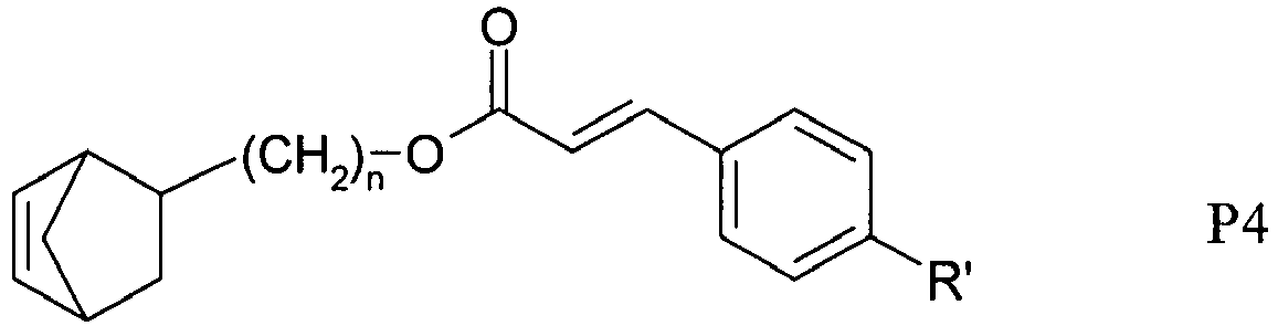

- The organic electronic device according to one or more of claims 1 to 7, wherein the polycycloolefinic polymer comprises one or more distinct types of repeating units of formula I

- The organic electronic device according to claim 8, wherein the polycycloolefinic polymer comprises one or more distinct types of repeating units formed from norbornene-type monomers independently selected from the following formulae:




- The organic electronic device according to claim 8 or 9, wherein the polycycloolefinic polymer comprises one or more distinct types of repeating units formed from norbornene-type monomers independently selected from the following formulae:


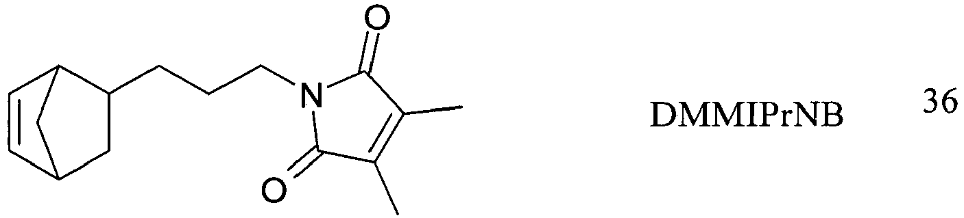


- The organic electronic device according to one or more of claims 1 to 10, wherein the bank structures comprise two or more distinct polycycloolefinic polymers having one or more distinct types of repeating units of formula I

- The organic electronic device according to one or more of claims 1 to 11, wherein the bank structures are derived from a polymer composition comprising one or more of a solvent, a crosslinking agent, an optional reactive solvent, a stabilizer, a UV sensitizer, an adhesion promoter, and a thermal sensitizer.
- The organic electronic device according to claim 12, wherein the polymer composition comprises a compound selected of formula III1 or III2
P-A"-X'-A"-P III1
H4-cC(A"-P)c III2
wherein X' is O, S, NH or a single bond, A" is a single bond or a connecting, spacer or bridging group selected from (CZ2)n, (CH2)n-(CH=CH)p-(CH2)n, (CH2)n-O-(CH2)n, (CH2)n-C6Q10-(CH2)n, and C(O), where each n is independently an integer from 0 to 12, p is an integer from 1-6, Z is independently H or F, C6Q10 is cyclohexyl that is substituted with Q, Q is independently H, F, CH3, CF3 or OCH3, P is a crosslinkable group as defined in claim 5, and c is 2, 3 or 4, and where in formula III1 at least one of X' and the two groups A" is not a single bond. - The organic electronic device according claim 13, wherein the compound of formula III1 is selected of formula C1

- The organic electronic device according to one or more of claims 12 to 16, wherein the polymer composition comprises a compound of formula IV
G1-A"-G2 IV
wherein G1 is a surface active group, A" is a single bond or a connecting, spacer or bridging group, and G2 is a crosslinkable group or a non-reactive compatibilizing group. - The organic electronic device according to claim 15, wherein G1 is a surface-active group of the formula -SiR12R13R14, or a group of the formula -NH-SiR12R13R14, wherein R12, R13 and R14 are each independently selected from halogen, silazane, C1-C12-alkoxy, C1-C12-alkylamino, optionally substituted C5-C20-aryloxy and optionally substituted C2-C20-heteroaryloxy, and wherein one or two of R12, R13 and R14 may also denote C1-C12-alkyl, optionally substituted C5-C20-aryl or optionally substituted C2-C20-heteroaryl,
G2 is a crosslinkable group selected from a maleimide, a 3-monoalkyl-maleimide, a 3,4-dialkylmaleimide, an epoxy, a vinyl, an acetyl, an indenyl, a cinnamate or a coumarin group, or comprises a substituted or unsubstituted maleimide portion, an epoxide portion, a vinyl portion, an acetylene portion, an indenyl portion, a cinnamate portion or a coumarin portion, and
A" is a single bond or a connecting, spacer or bridging group selected from (CZ2)n, (CH2)n-(CH=CH)p-(CH2)n, (CH2)n-O, (CH2)n-O-(CH2)n, (CH2)n-C6Q4-(CH2)n, (CH2)n-C6Q10-(CH2)n and C(O)-O, where each n is independently an integer from 0 to 12, p is an integer from 1-6, Z is independently H or F, C6Q4 is phenyl that is substituted with Q, C6Q10 is cyclohexyl that is substituted with Q, Q is independently H, F, CH3, CF3 or OCH3. - The organic electronic device according to claim 16, wherein the compound of formula IV is selected of formula A1:

- The organic electronic device according to one or more of claims 1 to 17, which is a top gate OFET or bottom gate OFET.
- The organic electronic device according to one or more of claims 1 to 18, which comprises a substrate (1), a gate electrode (2), a dielectric layer (3) serving as gate insulator, source and drain electrodes (4) that are spaced apart with a channel region (7) located therebetween, first and second bank structures (5a, 5b) that are patterned such that they define a well (8) that extends over the channel region (7), and an OSC layer (6) provided in the channel region (7), wherein the bank structures (5a, 5b) are derived from a polycycloolefinic polymer or a polymer composition as defined in one or more of claims 1 to 17.
- A process for preparing an electronic device according to claim 19, which comprises the following steps:a) forming gate electrode (2) on a substrate (1),b) depositing a layer of dielectric material (3) on the gate electrode (2),c) forming source and drain electrodes (4) on the dielectric layer (3) such that they are spaced apart with a channel region (7) located therebetween,d) forming bank structures (5a, 5b) by depositing a bank structure material comprising a polycycloolefinic polymer or a polymer composition as defined in one or more of claims 1 to 17 on the source and drain electrodes (4), thereby defining a well (8) that extends over the channel region (7),e) depositing a layer of semiconductor material (6) in the well (8) formed by the bank structures (5a, 5b) and onto the source and drain electrodes (4).
- The organic electronic device according to one or more of claims 1 to 18, which comprises a substrate (1), source and drain electrodes (4) that are spaced apart with a channel region (not shown) located therebetween, first and second bank structures (5a, 5b) that are patterned such that they define a well (8) that extends over the channel region, an OSC layer (6) provided in the channel region (7), a dielectric layer (3) serving as gate insulator, and gate electrode (2), wherein the bank structures (5a, 5b) are derived from a polycycloolefinic polymer or a polymer composition as defined in one or more of claims 1 to 17.
- A process for preparing an electronic device according to claim 21, which comprises the following stepsa) forming source and drain electrodes (4) on a substrate (1) such that they are spaced apart with a channel region located therebetween,b) forming bank structures (5a, 5b) by depositing bank structure material comprising a polycycloolefinic polymer or a polymer composition as defined in one or more of claims 1 to 16 on the source and drain electrodes (4), thereby defining a well (8) that extends over the channel region,c) depositing a layer of semiconductor material (6) in the well (8) formed by the bank structures (5a, 5b) and onto the source and drain electrodes (4),d) depositing a layer of dielectric material (3) on the semiconductor layer (6),e) forming gate electrode (2) on the dielectric layer (3).
- The organic electronic device or process according to one or more of claims 1 to 21, wherein the bank structures are formed as single layers comprising a polycycloolefinic polymer.
- A product or assembly comprising an organic electronic device according to one or more of claims 1 to 19, 21 or 23, which is an Integrated Circuit (IC), a Radio Frequency Identification (RFID) tag, a security marking or security device containing an RFID tag, a Flat Panel Display (FPD), a backplane of an FPD, a backlight of an FPD, an electrophotographic device, an electrophotographic recording device, an organic memory device, a sensor, a biosensor or a biochip.
Priority Applications (1)
| Application Number | Priority Date | Filing Date | Title |
|---|---|---|---|
| EP13720235.4A EP2841483B1 (en) | 2012-04-25 | 2013-04-18 | Bank structures for organic electronic devices |
Applications Claiming Priority (4)
| Application Number | Priority Date | Filing Date | Title |
|---|---|---|---|
| US201261637988P | 2012-04-25 | 2012-04-25 | |
| EP12002925 | 2012-04-26 | ||
| PCT/EP2013/001147 WO2013159881A2 (en) | 2012-04-25 | 2013-04-18 | Bank structures for organic electronic devices |
| EP13720235.4A EP2841483B1 (en) | 2012-04-25 | 2013-04-18 | Bank structures for organic electronic devices |
Publications (2)
| Publication Number | Publication Date |
|---|---|
| EP2841483A2 EP2841483A2 (en) | 2015-03-04 |
| EP2841483B1 true EP2841483B1 (en) | 2018-10-03 |
Family
ID=49476507
Family Applications (1)
| Application Number | Title | Priority Date | Filing Date |
|---|---|---|---|
| EP13720235.4A Active EP2841483B1 (en) | 2012-04-25 | 2013-04-18 | Bank structures for organic electronic devices |
Country Status (11)
| Country | Link |
|---|---|
| US (1) | US9331281B2 (en) |
| EP (1) | EP2841483B1 (en) |
| JP (1) | JP6262204B2 (en) |
| KR (1) | KR102082019B1 (en) |
| CN (1) | CN104245783B (en) |
| GB (1) | GB2517104A (en) |
| HK (1) | HK1202566A1 (en) |
| RU (1) | RU2014147079A (en) |
| SG (1) | SG11201406802VA (en) |
| TW (1) | TWI571474B (en) |
| WO (1) | WO2013159881A2 (en) |
Families Citing this family (16)
| Publication number | Priority date | Publication date | Assignee | Title |
|---|---|---|---|---|
| WO2014030354A1 (en) * | 2012-08-23 | 2014-02-27 | パナソニック株式会社 | Organic electronic device manufacturing method and organic el device manufacturing method |
| WO2015135622A1 (en) * | 2014-03-12 | 2015-09-17 | Merck Patent Gmbh | Organic electronic compositions and device thereof |
| RU2610606C2 (en) * | 2014-12-25 | 2017-02-14 | Акционерное общество "Государственный научно-исследовательский и проектный институт редкометаллической промышленности "Гиредмет" | Process for obtaining of composite material based on polymer matrices for microelectronics |
| WO2016159358A1 (en) * | 2015-04-03 | 2016-10-06 | 日産化学工業株式会社 | Photocrosslinkable group-containing composition for coating stepped substrate |
| JP6505857B2 (en) * | 2015-09-24 | 2019-04-24 | 富士フイルム株式会社 | Organic thin film transistor and method of manufacturing organic thin film transistor |
| DE102015119939A1 (en) | 2015-11-18 | 2017-05-18 | ALTANA Aktiengesellschaft | Crosslinkable polymeric materials for dielectric layers in electronic components |
| US9546977B1 (en) * | 2015-12-28 | 2017-01-17 | International Business Machines Corporation | Junction field effect transistor based biosensor |
| WO2018033510A2 (en) | 2016-08-17 | 2018-02-22 | Merck Patent Gmbh | Electronic device with bank structures |
| US20230276685A9 (en) * | 2016-08-26 | 2023-08-31 | Najing Technology Corporation Limited | Manufacturing method for light emitting device, light emitting device, and hybrid light emitting device |
| EP3589427A1 (en) * | 2017-03-02 | 2020-01-08 | The Regents of The University of California | Simultaneous doctor blading of different colored light emitting components |
| WO2018212960A1 (en) * | 2017-05-17 | 2018-11-22 | Apple Inc. | Organic light-emitting diode display with reduced lateral leakage |
| KR102355529B1 (en) * | 2017-08-07 | 2022-01-26 | 삼성디스플레이 주식회사 | Organic electroluminescence display device |
| US10453907B2 (en) * | 2017-08-21 | 2019-10-22 | Wuhan China Star Optoelectronics Semiconductor Display Technology Co., Ltd. | OLED device and method for fabricating the same |
| US20210284812A1 (en) * | 2018-06-28 | 2021-09-16 | Merck Patent Gmbh | Method for producing an electronic device |
| TWI889955B (en) * | 2021-02-15 | 2025-07-11 | 日商住友電木股份有限公司 | Photosensitive resin composition, cured film and semiconductor device |
| TW202530282A (en) * | 2023-09-11 | 2025-08-01 | 美商普羅梅勒斯有限公司 | Uv-nanoimprinted lithographic devices made from polycycloolefinic polymers for microfluidics |
Family Cites Families (27)
| Publication number | Priority date | Publication date | Assignee | Title |
|---|---|---|---|---|
| GB1278780A (en) | 1968-12-24 | 1972-06-21 | Agfa Gevaert | Photodimerisation and photopolymerisation of bis-maleimides |
| US5468819A (en) | 1993-11-16 | 1995-11-21 | The B.F. Goodrich Company | Process for making polymers containing a norbornene repeating unit by addition polymerization using an organo (nickel or palladium) complex |
| GB9726810D0 (en) | 1997-12-19 | 1998-02-18 | Zeneca Ltd | Compounds composition & use |
| US6538087B2 (en) | 2000-07-28 | 2003-03-25 | Promerus, Llc | Polymeric compositions for forming optical waveguides; optical waveguides formed therefrom; and methods for making same |
| US6656611B2 (en) | 2001-07-20 | 2003-12-02 | Osram Opto Semiconductors Gmbh | Structure-defining material for OLEDs |
| US6690029B1 (en) | 2001-08-24 | 2004-02-10 | University Of Kentucky Research Foundation | Substituted pentacenes and electronic devices made with substituted pentacenes |
| AU2002343058A1 (en) | 2001-12-19 | 2003-06-30 | Merck Patent Gmbh | Organic field effect transistor with an organic dielectric |
| KR100432544B1 (en) | 2002-03-18 | 2004-05-24 | 박병주 | Matrix-Type Three-Terminal Organic EL Display Device |
| US20060020068A1 (en) * | 2004-07-07 | 2006-01-26 | Edmund Elce | Photosensitive compositions based on polycyclic polymers for low stress, high temperature films |
| US7674847B2 (en) | 2003-02-21 | 2010-03-09 | Promerus Llc | Vinyl addition polycyclic olefin polymers prepared with non-olefinic chain transfer agents and uses thereof |
| ATE475971T1 (en) | 2003-11-28 | 2010-08-15 | Merck Patent Gmbh | ORGANIC SEMICONDUCTOR LAYER FORMULATIONS WITH POLYACENES AND ORGANIC BINDER POLYMERS |
| US7385221B1 (en) | 2005-03-08 | 2008-06-10 | University Of Kentucky Research Foundation | Silylethynylated heteroacenes and electronic devices made therewith |
| KR101209046B1 (en) | 2005-07-27 | 2012-12-06 | 삼성디스플레이 주식회사 | Thin film transistor substrate and method of making thin film transistor substrate |
| WO2007023272A1 (en) | 2005-08-23 | 2007-03-01 | Cambridge Display Technology Limited | Organic electronic device structures and fabrication methods |
| KR100718152B1 (en) | 2006-02-11 | 2007-05-14 | 삼성전자주식회사 | Organic light emitting diodes and manufacturing method |
| CN101622289A (en) * | 2006-12-06 | 2010-01-06 | 普罗米鲁斯有限责任公司 | Directly photodefinable polymer compositions and methods thereof |
| US8053515B2 (en) | 2006-12-06 | 2011-11-08 | Promerus Llc | Directly photodefinable polymer compositions and methods thereof |
| EP1933393A1 (en) | 2006-12-13 | 2008-06-18 | Samsung SDI Co., Ltd. | Method of manufacturing a substrate for an electronic device |
| KR100814407B1 (en) * | 2007-02-08 | 2008-03-18 | 삼성전자주식회사 | Composition for forming fine pattern and method of forming pattern using same |
| KR101062108B1 (en) | 2007-03-26 | 2011-09-02 | 파이오니아 가부시키가이샤 | Organic semiconductor device and manufacturing method thereof |
| GB2449926A (en) * | 2007-06-08 | 2008-12-10 | Seiko Epson Corp | Method for manufacturing an electrolyte pattern |
| JP2011501361A (en) | 2007-10-15 | 2011-01-06 | イー・アイ・デュポン・ドウ・ヌムール・アンド・カンパニー | Backplane structure for solution-processed electronic devices |
| GB2455747B (en) | 2007-12-19 | 2011-02-09 | Cambridge Display Tech Ltd | Electronic devices and methods of making the same using solution processing techniques |
| GB2458454B (en) | 2008-03-14 | 2011-03-16 | Cambridge Display Tech Ltd | Electronic devices and methods of making the same using solution processing techniques |
| GB2462845B (en) | 2008-08-21 | 2011-07-27 | Cambridge Display Tech Ltd | Organic electronic devices and methods of making the same using solution processing techniques |
| WO2012028279A1 (en) * | 2010-09-02 | 2012-03-08 | Merck Patent Gmbh | Gate insulator layer for electronic devices |
| KR20130114120A (en) | 2010-09-02 | 2013-10-16 | 메르크 파텐트 게엠베하 | Interlayer for electronic devices |
-
2013
- 2013-04-18 JP JP2015507411A patent/JP6262204B2/en active Active
- 2013-04-18 HK HK15103229.0A patent/HK1202566A1/en unknown
- 2013-04-18 KR KR1020147032849A patent/KR102082019B1/en active Active
- 2013-04-18 WO PCT/EP2013/001147 patent/WO2013159881A2/en not_active Ceased
- 2013-04-18 SG SG11201406802VA patent/SG11201406802VA/en unknown
- 2013-04-18 GB GB1420616.3A patent/GB2517104A/en not_active Withdrawn
- 2013-04-18 RU RU2014147079A patent/RU2014147079A/en not_active Application Discontinuation
- 2013-04-18 EP EP13720235.4A patent/EP2841483B1/en active Active
- 2013-04-18 CN CN201380021628.3A patent/CN104245783B/en active Active
- 2013-04-24 US US13/869,436 patent/US9331281B2/en active Active
- 2013-04-25 TW TW102114882A patent/TWI571474B/en active
Non-Patent Citations (1)
| Title |
|---|
| None * |
Also Published As
| Publication number | Publication date |
|---|---|
| US9331281B2 (en) | 2016-05-03 |
| WO2013159881A2 (en) | 2013-10-31 |
| JP2015523708A (en) | 2015-08-13 |
| US20130285026A1 (en) | 2013-10-31 |
| SG11201406802VA (en) | 2014-11-27 |
| WO2013159881A3 (en) | 2013-12-19 |
| CN104245783B (en) | 2017-12-12 |
| KR102082019B1 (en) | 2020-04-14 |
| RU2014147079A (en) | 2016-06-20 |
| CN104245783A (en) | 2014-12-24 |
| KR20150013583A (en) | 2015-02-05 |
| WO2013159881A9 (en) | 2014-02-06 |
| TW201400515A (en) | 2014-01-01 |
| HK1202566A1 (en) | 2015-10-02 |
| GB2517104A (en) | 2015-02-11 |
| EP2841483A2 (en) | 2015-03-04 |
| TWI571474B (en) | 2017-02-21 |
| GB201420616D0 (en) | 2015-01-07 |
| JP6262204B2 (en) | 2018-01-17 |
Similar Documents
| Publication | Publication Date | Title |
|---|---|---|
| US9331281B2 (en) | Bank structures for organic electronic devices | |
| EP2904648B1 (en) | Passivation layers for organic electronic devices | |
| EP2814855B1 (en) | Planarization layer for organic electronic devices | |
| US9923035B2 (en) | Method for producing organic electronic devices with bank structures, bank structures and electronic devices produced therewith | |
| EP2893575B1 (en) | Process of surface modification of dielectric structures in organic electronic devices |
Legal Events
| Date | Code | Title | Description |
|---|---|---|---|
| PUAI | Public reference made under article 153(3) epc to a published international application that has entered the european phase |
Free format text: ORIGINAL CODE: 0009012 |
|
| 17P | Request for examination filed |
Effective date: 20140903 |
|
| AK | Designated contracting states |
Kind code of ref document: A2 Designated state(s): AL AT BE BG CH CY CZ DE DK EE ES FI FR GB GR HR HU IE IS IT LI LT LU LV MC MK MT NL NO PL PT RO RS SE SI SK SM TR |
|
| AX | Request for extension of the european patent |
Extension state: BA ME |
|
| DAX | Request for extension of the european patent (deleted) | ||
| STAA | Information on the status of an ep patent application or granted ep patent |
Free format text: STATUS: EXAMINATION IS IN PROGRESS |
|
| 17Q | First examination report despatched |
Effective date: 20171013 |
|
| GRAP | Despatch of communication of intention to grant a patent |
Free format text: ORIGINAL CODE: EPIDOSNIGR1 |
|
| STAA | Information on the status of an ep patent application or granted ep patent |
Free format text: STATUS: GRANT OF PATENT IS INTENDED |
|
| INTG | Intention to grant announced |
Effective date: 20180430 |
|
| GRAS | Grant fee paid |
Free format text: ORIGINAL CODE: EPIDOSNIGR3 |
|
| GRAJ | Information related to disapproval of communication of intention to grant by the applicant or resumption of examination proceedings by the epo deleted |
Free format text: ORIGINAL CODE: EPIDOSDIGR1 |
|
| GRAL | Information related to payment of fee for publishing/printing deleted |
Free format text: ORIGINAL CODE: EPIDOSDIGR3 |
|
| STAA | Information on the status of an ep patent application or granted ep patent |
Free format text: STATUS: EXAMINATION IS IN PROGRESS |
|
| INTC | Intention to grant announced (deleted) | ||
| GRAR | Information related to intention to grant a patent recorded |
Free format text: ORIGINAL CODE: EPIDOSNIGR71 |
|
| STAA | Information on the status of an ep patent application or granted ep patent |
Free format text: STATUS: GRANT OF PATENT IS INTENDED |
|
| GRAA | (expected) grant |
Free format text: ORIGINAL CODE: 0009210 |
|
| STAA | Information on the status of an ep patent application or granted ep patent |
Free format text: STATUS: THE PATENT HAS BEEN GRANTED |
|
| AK | Designated contracting states |
Kind code of ref document: B1 Designated state(s): AL AT BE BG CH CY CZ DE DK EE ES FI FR GB GR HR HU IE IS IT LI LT LU LV MC MK MT NL NO PL PT RO RS SE SI SK SM TR |
|
| INTG | Intention to grant announced |
Effective date: 20180828 |
|
| REG | Reference to a national code |
Ref country code: GB Ref legal event code: FG4D |
|
| REG | Reference to a national code |
Ref country code: CH Ref legal event code: EP Ref country code: AT Ref legal event code: REF Ref document number: 1048510 Country of ref document: AT Kind code of ref document: T Effective date: 20181015 |
|
| REG | Reference to a national code |
Ref country code: IE Ref legal event code: FG4D Ref country code: DE Ref legal event code: R096 Ref document number: 602013044452 Country of ref document: DE |
|
| REG | Reference to a national code |
Ref country code: NL Ref legal event code: MP Effective date: 20181003 |
|
| REG | Reference to a national code |
Ref country code: LT Ref legal event code: MG4D |
|
| REG | Reference to a national code |
Ref country code: AT Ref legal event code: MK05 Ref document number: 1048510 Country of ref document: AT Kind code of ref document: T Effective date: 20181003 |
|
| PG25 | Lapsed in a contracting state [announced via postgrant information from national office to epo] |
Ref country code: NL Free format text: LAPSE BECAUSE OF FAILURE TO SUBMIT A TRANSLATION OF THE DESCRIPTION OR TO PAY THE FEE WITHIN THE PRESCRIBED TIME-LIMIT Effective date: 20181003 |
|
| PG25 | Lapsed in a contracting state [announced via postgrant information from national office to epo] |
Ref country code: ES Free format text: LAPSE BECAUSE OF FAILURE TO SUBMIT A TRANSLATION OF THE DESCRIPTION OR TO PAY THE FEE WITHIN THE PRESCRIBED TIME-LIMIT Effective date: 20181003 Ref country code: AT Free format text: LAPSE BECAUSE OF FAILURE TO SUBMIT A TRANSLATION OF THE DESCRIPTION OR TO PAY THE FEE WITHIN THE PRESCRIBED TIME-LIMIT Effective date: 20181003 Ref country code: CZ Free format text: LAPSE BECAUSE OF FAILURE TO SUBMIT A TRANSLATION OF THE DESCRIPTION OR TO PAY THE FEE WITHIN THE PRESCRIBED TIME-LIMIT Effective date: 20181003 Ref country code: IS Free format text: LAPSE BECAUSE OF FAILURE TO SUBMIT A TRANSLATION OF THE DESCRIPTION OR TO PAY THE FEE WITHIN THE PRESCRIBED TIME-LIMIT Effective date: 20190203 Ref country code: NO Free format text: LAPSE BECAUSE OF FAILURE TO SUBMIT A TRANSLATION OF THE DESCRIPTION OR TO PAY THE FEE WITHIN THE PRESCRIBED TIME-LIMIT Effective date: 20190103 Ref country code: BG Free format text: LAPSE BECAUSE OF FAILURE TO SUBMIT A TRANSLATION OF THE DESCRIPTION OR TO PAY THE FEE WITHIN THE PRESCRIBED TIME-LIMIT Effective date: 20190103 Ref country code: PL Free format text: LAPSE BECAUSE OF FAILURE TO SUBMIT A TRANSLATION OF THE DESCRIPTION OR TO PAY THE FEE WITHIN THE PRESCRIBED TIME-LIMIT Effective date: 20181003 Ref country code: LT Free format text: LAPSE BECAUSE OF FAILURE TO SUBMIT A TRANSLATION OF THE DESCRIPTION OR TO PAY THE FEE WITHIN THE PRESCRIBED TIME-LIMIT Effective date: 20181003 Ref country code: FI Free format text: LAPSE BECAUSE OF FAILURE TO SUBMIT A TRANSLATION OF THE DESCRIPTION OR TO PAY THE FEE WITHIN THE PRESCRIBED TIME-LIMIT Effective date: 20181003 Ref country code: HR Free format text: LAPSE BECAUSE OF FAILURE TO SUBMIT A TRANSLATION OF THE DESCRIPTION OR TO PAY THE FEE WITHIN THE PRESCRIBED TIME-LIMIT Effective date: 20181003 Ref country code: LV Free format text: LAPSE BECAUSE OF FAILURE TO SUBMIT A TRANSLATION OF THE DESCRIPTION OR TO PAY THE FEE WITHIN THE PRESCRIBED TIME-LIMIT Effective date: 20181003 |
|
| PG25 | Lapsed in a contracting state [announced via postgrant information from national office to epo] |
Ref country code: SE Free format text: LAPSE BECAUSE OF FAILURE TO SUBMIT A TRANSLATION OF THE DESCRIPTION OR TO PAY THE FEE WITHIN THE PRESCRIBED TIME-LIMIT Effective date: 20181003 Ref country code: RS Free format text: LAPSE BECAUSE OF FAILURE TO SUBMIT A TRANSLATION OF THE DESCRIPTION OR TO PAY THE FEE WITHIN THE PRESCRIBED TIME-LIMIT Effective date: 20181003 Ref country code: AL Free format text: LAPSE BECAUSE OF FAILURE TO SUBMIT A TRANSLATION OF THE DESCRIPTION OR TO PAY THE FEE WITHIN THE PRESCRIBED TIME-LIMIT Effective date: 20181003 Ref country code: PT Free format text: LAPSE BECAUSE OF FAILURE TO SUBMIT A TRANSLATION OF THE DESCRIPTION OR TO PAY THE FEE WITHIN THE PRESCRIBED TIME-LIMIT Effective date: 20190203 Ref country code: GR Free format text: LAPSE BECAUSE OF FAILURE TO SUBMIT A TRANSLATION OF THE DESCRIPTION OR TO PAY THE FEE WITHIN THE PRESCRIBED TIME-LIMIT Effective date: 20190104 |
|
| REG | Reference to a national code |
Ref country code: DE Ref legal event code: R097 Ref document number: 602013044452 Country of ref document: DE |
|
| PG25 | Lapsed in a contracting state [announced via postgrant information from national office to epo] |
Ref country code: DK Free format text: LAPSE BECAUSE OF FAILURE TO SUBMIT A TRANSLATION OF THE DESCRIPTION OR TO PAY THE FEE WITHIN THE PRESCRIBED TIME-LIMIT Effective date: 20181003 Ref country code: IT Free format text: LAPSE BECAUSE OF FAILURE TO SUBMIT A TRANSLATION OF THE DESCRIPTION OR TO PAY THE FEE WITHIN THE PRESCRIBED TIME-LIMIT Effective date: 20181003 |
|
| PLBE | No opposition filed within time limit |
Free format text: ORIGINAL CODE: 0009261 |
|
| STAA | Information on the status of an ep patent application or granted ep patent |
Free format text: STATUS: NO OPPOSITION FILED WITHIN TIME LIMIT |
|
| PG25 | Lapsed in a contracting state [announced via postgrant information from national office to epo] |
Ref country code: SM Free format text: LAPSE BECAUSE OF FAILURE TO SUBMIT A TRANSLATION OF THE DESCRIPTION OR TO PAY THE FEE WITHIN THE PRESCRIBED TIME-LIMIT Effective date: 20181003 Ref country code: EE Free format text: LAPSE BECAUSE OF FAILURE TO SUBMIT A TRANSLATION OF THE DESCRIPTION OR TO PAY THE FEE WITHIN THE PRESCRIBED TIME-LIMIT Effective date: 20181003 Ref country code: RO Free format text: LAPSE BECAUSE OF FAILURE TO SUBMIT A TRANSLATION OF THE DESCRIPTION OR TO PAY THE FEE WITHIN THE PRESCRIBED TIME-LIMIT Effective date: 20181003 Ref country code: SK Free format text: LAPSE BECAUSE OF FAILURE TO SUBMIT A TRANSLATION OF THE DESCRIPTION OR TO PAY THE FEE WITHIN THE PRESCRIBED TIME-LIMIT Effective date: 20181003 |
|
| 26N | No opposition filed |
Effective date: 20190704 |
|
| PG25 | Lapsed in a contracting state [announced via postgrant information from national office to epo] |
Ref country code: SI Free format text: LAPSE BECAUSE OF FAILURE TO SUBMIT A TRANSLATION OF THE DESCRIPTION OR TO PAY THE FEE WITHIN THE PRESCRIBED TIME-LIMIT Effective date: 20181003 |
|
| REG | Reference to a national code |
Ref country code: CH Ref legal event code: PL |
|
| REG | Reference to a national code |
Ref country code: BE Ref legal event code: MM Effective date: 20190430 |
|
| PG25 | Lapsed in a contracting state [announced via postgrant information from national office to epo] |
Ref country code: LU Free format text: LAPSE BECAUSE OF NON-PAYMENT OF DUE FEES Effective date: 20190418 Ref country code: MC Free format text: LAPSE BECAUSE OF FAILURE TO SUBMIT A TRANSLATION OF THE DESCRIPTION OR TO PAY THE FEE WITHIN THE PRESCRIBED TIME-LIMIT Effective date: 20181003 |
|
| PG25 | Lapsed in a contracting state [announced via postgrant information from national office to epo] |
Ref country code: CH Free format text: LAPSE BECAUSE OF NON-PAYMENT OF DUE FEES Effective date: 20190430 Ref country code: LI Free format text: LAPSE BECAUSE OF NON-PAYMENT OF DUE FEES Effective date: 20190430 |
|
| PG25 | Lapsed in a contracting state [announced via postgrant information from national office to epo] |
Ref country code: BE Free format text: LAPSE BECAUSE OF NON-PAYMENT OF DUE FEES Effective date: 20190430 Ref country code: FR Free format text: LAPSE BECAUSE OF NON-PAYMENT OF DUE FEES Effective date: 20190430 |
|
| PG25 | Lapsed in a contracting state [announced via postgrant information from national office to epo] |
Ref country code: TR Free format text: LAPSE BECAUSE OF FAILURE TO SUBMIT A TRANSLATION OF THE DESCRIPTION OR TO PAY THE FEE WITHIN THE PRESCRIBED TIME-LIMIT Effective date: 20181003 |
|
| PG25 | Lapsed in a contracting state [announced via postgrant information from national office to epo] |
Ref country code: IE Free format text: LAPSE BECAUSE OF NON-PAYMENT OF DUE FEES Effective date: 20190418 |
|
| REG | Reference to a national code |
Ref country code: GB Ref legal event code: 732E Free format text: REGISTERED BETWEEN 20200521 AND 20200527 |
|
| PG25 | Lapsed in a contracting state [announced via postgrant information from national office to epo] |
Ref country code: CY Free format text: LAPSE BECAUSE OF FAILURE TO SUBMIT A TRANSLATION OF THE DESCRIPTION OR TO PAY THE FEE WITHIN THE PRESCRIBED TIME-LIMIT Effective date: 20181003 |
|
| PG25 | Lapsed in a contracting state [announced via postgrant information from national office to epo] |
Ref country code: HU Free format text: LAPSE BECAUSE OF FAILURE TO SUBMIT A TRANSLATION OF THE DESCRIPTION OR TO PAY THE FEE WITHIN THE PRESCRIBED TIME-LIMIT; INVALID AB INITIO Effective date: 20130418 Ref country code: MT Free format text: LAPSE BECAUSE OF FAILURE TO SUBMIT A TRANSLATION OF THE DESCRIPTION OR TO PAY THE FEE WITHIN THE PRESCRIBED TIME-LIMIT Effective date: 20181003 |
|
| PG25 | Lapsed in a contracting state [announced via postgrant information from national office to epo] |
Ref country code: MK Free format text: LAPSE BECAUSE OF FAILURE TO SUBMIT A TRANSLATION OF THE DESCRIPTION OR TO PAY THE FEE WITHIN THE PRESCRIBED TIME-LIMIT Effective date: 20181003 |
|
| P01 | Opt-out of the competence of the unified patent court (upc) registered |
Effective date: 20230528 |
|
| REG | Reference to a national code |
Ref country code: GB Ref legal event code: 732E Free format text: REGISTERED BETWEEN 20230615 AND 20230621 |
|
| REG | Reference to a national code |
Ref country code: DE Ref legal event code: R081 Ref document number: 602013044452 Country of ref document: DE Owner name: PROMERUS LLC, BRECKSVILLE, US Free format text: FORMER OWNERS: MERCK PATENT GMBH, 64293 DARMSTADT, DE; PROMERUS LLC, BRECKSVILLE, OHIO, US Ref country code: DE Ref legal event code: R081 Ref document number: 602013044452 Country of ref document: DE Owner name: FLEXENABLE TECHNOLOGY LTD., GB Free format text: FORMER OWNERS: MERCK PATENT GMBH, 64293 DARMSTADT, DE; PROMERUS LLC, BRECKSVILLE, OHIO, US |
|
| PGFP | Annual fee paid to national office [announced via postgrant information from national office to epo] |
Ref country code: DE Payment date: 20251022 Year of fee payment: 13 |
|
| PGFP | Annual fee paid to national office [announced via postgrant information from national office to epo] |
Ref country code: GB Payment date: 20251022 Year of fee payment: 13 |