EP2840307A1 - Illumination device and display device - Google Patents
Illumination device and display device Download PDFInfo
- Publication number
- EP2840307A1 EP2840307A1 EP14181095.2A EP14181095A EP2840307A1 EP 2840307 A1 EP2840307 A1 EP 2840307A1 EP 14181095 A EP14181095 A EP 14181095A EP 2840307 A1 EP2840307 A1 EP 2840307A1
- Authority
- EP
- European Patent Office
- Prior art keywords
- lens
- leg
- substrate
- legs
- contact surface
- Prior art date
- Legal status (The legal status is an assumption and is not a legal conclusion. Google has not performed a legal analysis and makes no representation as to the accuracy of the status listed.)
- Withdrawn
Links
Images




Classifications
-
- H—ELECTRICITY
- H10—SEMICONDUCTOR DEVICES; ELECTRIC SOLID-STATE DEVICES NOT OTHERWISE PROVIDED FOR
- H10H—INORGANIC LIGHT-EMITTING SEMICONDUCTOR DEVICES HAVING POTENTIAL BARRIERS
- H10H20/00—Individual inorganic light-emitting semiconductor devices having potential barriers, e.g. light-emitting diodes [LED]
- H10H20/80—Constructional details
- H10H20/85—Packages
- H10H20/855—Optical field-shaping means, e.g. lenses
-
- F—MECHANICAL ENGINEERING; LIGHTING; HEATING; WEAPONS; BLASTING
- F21—LIGHTING
- F21V—FUNCTIONAL FEATURES OR DETAILS OF LIGHTING DEVICES OR SYSTEMS THEREOF; STRUCTURAL COMBINATIONS OF LIGHTING DEVICES WITH OTHER ARTICLES, NOT OTHERWISE PROVIDED FOR
- F21V17/00—Fastening of component parts of lighting devices, e.g. shades, globes, refractors, reflectors, filters, screens, grids or protective cages
- F21V17/10—Fastening of component parts of lighting devices, e.g. shades, globes, refractors, reflectors, filters, screens, grids or protective cages characterised by specific fastening means or way of fastening
- F21V17/101—Fastening of component parts of lighting devices, e.g. shades, globes, refractors, reflectors, filters, screens, grids or protective cages characterised by specific fastening means or way of fastening permanently, e.g. welding, gluing or riveting
-
- F—MECHANICAL ENGINEERING; LIGHTING; HEATING; WEAPONS; BLASTING
- F21—LIGHTING
- F21V—FUNCTIONAL FEATURES OR DETAILS OF LIGHTING DEVICES OR SYSTEMS THEREOF; STRUCTURAL COMBINATIONS OF LIGHTING DEVICES WITH OTHER ARTICLES, NOT OTHERWISE PROVIDED FOR
- F21V5/00—Refractors for light sources
- F21V5/04—Refractors for light sources of lens shape
-
- G—PHYSICS
- G02—OPTICS
- G02B—OPTICAL ELEMENTS, SYSTEMS OR APPARATUS
- G02B19/00—Condensers, e.g. light collectors or similar non-imaging optics
- G02B19/0033—Condensers, e.g. light collectors or similar non-imaging optics characterised by the use
- G02B19/0047—Condensers, e.g. light collectors or similar non-imaging optics characterised by the use for use with a light source
- G02B19/0061—Condensers, e.g. light collectors or similar non-imaging optics characterised by the use for use with a light source the light source comprising a LED
-
- G—PHYSICS
- G02—OPTICS
- G02B—OPTICAL ELEMENTS, SYSTEMS OR APPARATUS
- G02B7/00—Mountings, adjusting means, or light-tight connections, for optical elements
- G02B7/02—Mountings, adjusting means, or light-tight connections, for optical elements for lenses
- G02B7/025—Mountings, adjusting means, or light-tight connections, for optical elements for lenses using glue
-
- G—PHYSICS
- G02—OPTICS
- G02F—OPTICAL DEVICES OR ARRANGEMENTS FOR THE CONTROL OF LIGHT BY MODIFICATION OF THE OPTICAL PROPERTIES OF THE MEDIA OF THE ELEMENTS INVOLVED THEREIN; NON-LINEAR OPTICS; FREQUENCY-CHANGING OF LIGHT; OPTICAL LOGIC ELEMENTS; OPTICAL ANALOGUE/DIGITAL CONVERTERS
- G02F1/00—Devices or arrangements for the control of the intensity, colour, phase, polarisation or direction of light arriving from an independent light source, e.g. switching, gating or modulating; Non-linear optics
- G02F1/01—Devices or arrangements for the control of the intensity, colour, phase, polarisation or direction of light arriving from an independent light source, e.g. switching, gating or modulating; Non-linear optics for the control of the intensity, phase, polarisation or colour
- G02F1/13—Devices or arrangements for the control of the intensity, colour, phase, polarisation or direction of light arriving from an independent light source, e.g. switching, gating or modulating; Non-linear optics for the control of the intensity, phase, polarisation or colour based on liquid crystals, e.g. single liquid crystal display cells
- G02F1/133—Constructional arrangements; Operation of liquid crystal cells; Circuit arrangements
- G02F1/1333—Constructional arrangements; Manufacturing methods
- G02F1/1335—Structural association of cells with optical devices, e.g. polarisers or reflectors
- G02F1/1336—Illuminating devices
- G02F1/133602—Direct backlight
- G02F1/133603—Direct backlight with LEDs
-
- F—MECHANICAL ENGINEERING; LIGHTING; HEATING; WEAPONS; BLASTING
- F21—LIGHTING
- F21Y—INDEXING SCHEME ASSOCIATED WITH SUBCLASSES F21K, F21L, F21S and F21V, RELATING TO THE FORM OR THE KIND OF THE LIGHT SOURCES OR OF THE COLOUR OF THE LIGHT EMITTED
- F21Y2103/00—Elongate light sources, e.g. fluorescent tubes
- F21Y2103/10—Elongate light sources, e.g. fluorescent tubes comprising a linear array of point-like light-generating elements
-
- F—MECHANICAL ENGINEERING; LIGHTING; HEATING; WEAPONS; BLASTING
- F21—LIGHTING
- F21Y—INDEXING SCHEME ASSOCIATED WITH SUBCLASSES F21K, F21L, F21S and F21V, RELATING TO THE FORM OR THE KIND OF THE LIGHT SOURCES OR OF THE COLOUR OF THE LIGHT EMITTED
- F21Y2115/00—Light-generating elements of semiconductor light sources
- F21Y2115/10—Light-emitting diodes [LED]
-
- G—PHYSICS
- G02—OPTICS
- G02F—OPTICAL DEVICES OR ARRANGEMENTS FOR THE CONTROL OF LIGHT BY MODIFICATION OF THE OPTICAL PROPERTIES OF THE MEDIA OF THE ELEMENTS INVOLVED THEREIN; NON-LINEAR OPTICS; FREQUENCY-CHANGING OF LIGHT; OPTICAL LOGIC ELEMENTS; OPTICAL ANALOGUE/DIGITAL CONVERTERS
- G02F1/00—Devices or arrangements for the control of the intensity, colour, phase, polarisation or direction of light arriving from an independent light source, e.g. switching, gating or modulating; Non-linear optics
- G02F1/01—Devices or arrangements for the control of the intensity, colour, phase, polarisation or direction of light arriving from an independent light source, e.g. switching, gating or modulating; Non-linear optics for the control of the intensity, phase, polarisation or colour
- G02F1/13—Devices or arrangements for the control of the intensity, colour, phase, polarisation or direction of light arriving from an independent light source, e.g. switching, gating or modulating; Non-linear optics for the control of the intensity, phase, polarisation or colour based on liquid crystals, e.g. single liquid crystal display cells
- G02F1/133—Constructional arrangements; Operation of liquid crystal cells; Circuit arrangements
- G02F1/1333—Constructional arrangements; Manufacturing methods
- G02F1/1335—Structural association of cells with optical devices, e.g. polarisers or reflectors
- G02F1/1336—Illuminating devices
- G02F1/133602—Direct backlight
- G02F1/133606—Direct backlight including a specially adapted diffusing, scattering or light controlling members
- G02F1/133607—Direct backlight including a specially adapted diffusing, scattering or light controlling members the light controlling member including light directing or refracting elements, e.g. prisms or lenses
-
- H—ELECTRICITY
- H10—SEMICONDUCTOR DEVICES; ELECTRIC SOLID-STATE DEVICES NOT OTHERWISE PROVIDED FOR
- H10H—INORGANIC LIGHT-EMITTING SEMICONDUCTOR DEVICES HAVING POTENTIAL BARRIERS
- H10H20/00—Individual inorganic light-emitting semiconductor devices having potential barriers, e.g. light-emitting diodes [LED]
- H10H20/01—Manufacture or treatment
- H10H20/036—Manufacture or treatment of packages
- H10H20/0363—Manufacture or treatment of packages of optical field-shaping means
Definitions
- the invention generally relates to an illumination device and a display device, and more particularly to a structure of a lens that widens a light-distribution angle of light emitted from a light-emitting diode (LED).
- LED light-emitting diode
- Conventional display devices such as a liquid crystal display device use a direct type backlight of that irradiates light to a display panel (for example, see Patent Literature 1).
- An LED and a lens that widens a light-distribution angle of light emitted from the LED are used for the backlight, but a positional relationship between the LED and the lens affects an optical characteristic of the backlight. Because of this, there is a need for position determination of the lens so that the positional relationship between the LED and the lens matches a design value.
- the lens is adhered to a substrate by an adhesive.
- the LED is mounted on the substrate.
- the lens is mounted on the substrate by a mounter (mounting device or tool to mount a lens on a substrate) seeking a center of the lens from an external shape of the lens by image processing, a mounting position of the lens being sought from a position of a recognition mark provided on the substrate, and the lens being mounted in the sought mounting position.
- Patent Literature 1 Japanese Unexamined Patent Application Publication No. 2012-204025
- the lens may not contact the substrate and may be spaced apart from the substrate. Because of this, the light-distribution angle of the light emitted from the LED does not coincide with the design value and, when this light is irradiated to the display panel, unevenness in brightness and variations in chromaticity occur.
- One or more embodiments of the invention are directed to an illumination device and a display device that reduces unevenness in brightness and variations in chromaticity in a display panel.
- An illumination device may comprise a substrate, a light-emitting diode (LED) disposed on the substrate, and a lens that faces the LED and widens a light-distribution angle of light emitted from the LED, wherein the lens may comprise a plurality of legs adhered to the substrate by an adhesive, and wherein each of the plurality of legs may comprise a contact surface that is curved in a convex shape.
- LED light-emitting diode
- the adhesive is more likely to flow to a side of the leg when pressing the leg of the lens to the substrate because the contact surface of the leg is curved in the convex shape. Because of this, for example, the leg of the lens and the substrate can be reliably contacted and the lens can be position-determined so a positional relationship between the LED and the lens matches a design value. Therefore, when the illumination device is used as a backlight of the display device, unevenness in brightness and variation in chromaticity in the display panel can be reduced.
- the contact surface of each of the plurality of legs may have a spherical cap shape.
- the leg of the lens can more easily contact the substrate at a point.
- the lens can be position-determined so the positional relationship between the LED and the lens matches the design value. Therefore, when the illumination device is used as the backlight of the display device, unevenness in brightness and variation in chromaticity in the display panel can be reduced.
- the contact surface of each leg may comprise a groove.
- the adhesive when pressing the leg of the lens to the substrate, the adhesive is more likely to flow to the side of the leg by being conducted along the groove.
- each leg may have a groove that extends in radially (or in a radial direction) from a central portion of the contact surface.
- the adhesive when pressing the leg of the lens to the substrate, the adhesive is more likely to flow to the side of the leg by being conducted along a groove from a center of the leg.
- a side surface of each of the plurality of legs may be an uneven surface.
- a surface area of the side surface of the leg of the lens can be increased. Therefore, compared to a situation where there is no unevenness on the side surface of the leg of the lens, shear strength generated between the leg of the lens and the adhesive can be increased. As a result, for example, the lens can be prevented from peeling from the substrate.
- a grain finish may be applied to the side surface of each leg.
- a surface area of the side surface of the leg of the lens can be increased by a simple manufacturing method.
- a display device is provided with a display panel and the illumination device described above that irradiates light to the display panel.
- the illumination device and the display device that make unevenness in brightness and variations in chromaticity less likely to occur in the display panel can be provided.
- a display device according to one or more embodiments of a first example will be described with reference to the drawings.
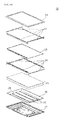
- FIG. 1A is an external view of a liquid crystal display 10 that is an example of the display device according to one or more embodiments of the invention.
- FIG. 1B is an exploded perspective view of the liquid crystal display 10 illustrated in FIG. 1A .
- the liquid crystal display 10 is provided with an enclosure 18, and the enclosure 18 comprises a front cabinet 11 and a rear frame 17.
- the front cabinet 11 is in a frame shape and covers an outer peripheral portion of a liquid crystal cell 13 (configuring a display panel) that will be described below.
- the front cabinet 11 is formed, for example, from resin.
- the rear frame 17 is disposed so as to cover a back surface side of the liquid crystal cell 13.
- a bezel 12 the liquid crystal cell 13, a cell guide 14, an optical sheet 15, a reflective sheet 16, and a backlight unit 19 are disposed inside the enclosure 18.
- the bezel 12 is disposed on a top surface side (that is, a side on which the liquid crystal cell 13 is disposed) of the cell guide 14 and covers an outer peripheral portion on a front surface side of the liquid crystal cell 13.
- the liquid crystal cell 13 is in a panel shape of a rectangular shape.
- the outer peripheral portion of the liquid crystal cell 13 is supported by a cell guide 14 of a frame shape.
- An image is displayed on the liquid crystal cell 13 by light from the backlight unit 19 that is irradiated to a back surface of the liquid crystal cell 13.
- the optical sheet 15 comprises a plurality of members, such as a diffuser panel and the like.
- the optical sheet 15 has, for example, a function of diffusing the light from the backlight unit 19.
- the reflective sheet 16 is disposed to cover an inner surface (that is, a surface on a side on which the liquid crystal cell 13 is disposed) of the rear frame 17.
- the reflective sheet 16 has a function of reflecting the light from the backlight unit 19 toward the back surface of the liquid crystal cell 13.
- the backlight unit 19 is an illumination device of a direct type method and irradiates light toward the back surface of the liquid crystal cell 13.
- the backlight unit 19 has one or more LED bars 20 (configuring the illumination device).
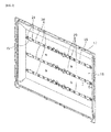
- FIG. 2 is a diagram enlarging a periphery of the backlight unit 19 according to one or more embodiments.
- the backlight unit 19 is configured, for example, by six LED bars 20. However, the number of the LED bars 20 is not limited thereto.
- the LED bar 20 has a substrate 22 and a plurality of LED units 28 mounted on the substrate 22.
- the substrate 22 is configured in a plate shape of an elongated shape.
- the plurality of LED units 28 is disposed in one row and at intervals along a lengthwise direction of the substrate 22.
- the substrate 22 is attached to the inner surface of the rear frame 17 by a double-sided tape having thermal conductivity (not illustrated).
- the substrate 22 is formed from a metal with high thermal conductivity, for example, aluminum.
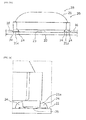
- FIG. 3A is a line A-A cross-sectional view of FIG. 2 according to one or more embodiments.
- FIG. 3B is an enlarged diagram of a leg 21a illustrated in FIG. 3A .
- FIG. 3C is an enlarged perspective view of the leg 21a.
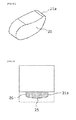
- FIG. 4 is a diagram of a lens 21 illustrated in FIG. 3A when viewed from a rear surface side (side of the substrate 22).
- each of the plurality of LED units 28 disposed on the LED bar 20 includes an LED 23 and the lens 21.
- the LED 23 is mounted on the substrate 22, and the lens 21 is disposed opposite the LED 23.
- the lens 21 fulfils a function of widening a light-distribution angle of light emitted from the LED 23.
- four legs 21a to 21d are formed on a peripheral portion of a rear surface of the lens 21.
- the four legs 21a to 21d are adhered to the substrate 22 by an adhesive 24. Illustrations of the leg 21b and the leg 21 d in FIG. 3A are omitted only for clarification purposes.
- the number of legs of the lens 21 is not limited to four and is sufficient if there exist three or more, for example.
- a contact surface 25 of the leg 21a is curved in a convex shape.
- the contact surface 25 has a circular shape
- a peripheral portion of the contact surface 25 is in a planar shape
- a shape of an inner side of the peripheral portion is a spherical cap shape.
- Contact surfaces of the other legs 21b to 21d also have shapes similar to the contact surface 25. Being curved overall in the convex shape indicates that, ideally, a portion that is 90% or more of the contact surface 25 is curved in the convex shape.
- the lens 21 is fixed to the substrate 22 in the following manner. That is, the adhesive 24 is applied in advance to a position on the substrate 22 where the legs 21 a to 21 d make contact.
- a mounter fixes the lens 21 to the substrate 22 by pressing the contact surface 25 of the legs 21a to 21d of the lens 21 to the substrate 22 applied with the adhesive 24.
- the contact surface 25 of the legs 21a to 21d is curved in a convex shape. Because of this, as illustrated in FIG. 3B , when pressing the leg 21a of the lens 21 to the substrate 22, a tip of the contact portion 25 first contacts the adhesive 24, and the contact surface 25 is pressed to the substrate 22 while the contact surface 25 pushes away the adhesive 24 to a side (direction of the arrows) of the leg 21a. That is, it becomes easier to flow the adhesive 24 to the side (direction of the arrows) of the leg 21a. Similarly, with the other legs 21b to 21d, it becomes easier to flow the adhesive 24 to a side of each leg.
- each leg of the lens 21 and the substrate 22 can reliably contact each other.
- a shape of the contact surface 25 of the legs 21a to 21d is a spherical cap shape, it becomes easier for each leg to contact the substrate 22 at a point.
- the lens 21 can be position-determined so a positional relationship between the LED 23 and the lens 21 matches a design value. Therefore, when the LED bar 20 is used as a backlight of the liquid crystal display 10, it is less likely for unevenness in brightness and variation in chromaticity to occur in the liquid crystal cell 13.
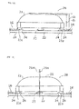
- FIGS. 5A and 5B are diagrams for describing an installation example of the lens 21 when the contact surface of each leg is of the planar shape.
- the contact surface is of the planar shape
- the mounter presses the legs 21a to 21d of the lens 21 to the substrate 22 applied with the adhesive 24 it is difficult to flow the adhesive 24 to the side of each leg because the contact surface and the adhesive 24 make contact at a surface from when adhesion begins. Because of this, as illustrated in FIG. 5A , the contact surface of each leg cannot be contacted to the substrate 22, and fixing occurs in a state of being floated from the substrate 22.
- a distance d2 from the substrate 22 to a tip of the lens 21 becomes greater than a distance d1 established by the design value.
- position determination of the lens 21 cannot be performed precisely, and unevenness in brightness and variation in chromaticity occur in the liquid crystal cell 13.
- the leg 21c contacts the substrate 22, but the leg 21a is also fixed in the state of being floated from the substrate 22.
- an optical axis 21m of the lens 21 becomes inclined relative to an optical axis 21n established by the design value. Because of this, position determination of the lens 21 cannot be performed precisely, and unevenness in brightness and variation in chromaticity occur in the liquid crystal cell 13.
- the lens 21 can reliably contact the substrate 22. Because of this, unevenness in brightness and variation in chromaticity can be reduced in the liquid crystal cell 13.
- FIG. 6A is an enlarged view of the leg 21a illustrated in FIG. 3A .
- FIG. 6B is an enlarged perspective view of the leg 21a.
- the shapes of the legs 21b to 21d are also similar.
- the entirety of the contact surface 25 may be curved in a convex shape. Specifically, the entirety of the contact surface 25 may be of a spherical cap shape.
- the contact surface 25 of each leg of the lens 21 is made to be of the spherical cap shape.
- a side surface of each leg may be uneven.
- FIG. 7 is an enlarged diagram of the leg 21a illustrated in FIG. 3A according to one or more embodiments.
- a side surface 26 of the leg 21a may be uneven.
- an uneven surface may be grainy, patterned, or the like.
- a grain finish may be applied to the side surface 26.
- the shape of the side surface 26 of the legs 21b to 21d may be similarly uneven.
- a surface area of the side surface 26 of the leg of the lens 21 can be increased. Therefore, shear strength generated between the leg of the lens 21 and the adhesive 24 can be increased compared to a situation where there is no unevenness on a side surface of a leg of a lens. As a result, the lens 21 can be prevented from peeling from the substrate 22. Moreover, by applying the grain finish on the side surface 26, the surface area of the side surface 26 can be increased by a simple manufacturing method.
- the shape of the side surface 26 is not limited to that which is illustrated and may be any shape so long it is uneven.
- the contact surface 25 of each leg of the lens 21 is made to be of the spherical cap shape. In one or more embodiments of a third example, the contact surface 25 is of the spherical cap shape and has a groove.
- FIG. 8 is an enlarged perspective view of the leg 21a of the lens 21 according to one or more embodiments.
- the shapes of the legs 21b to 21d are also similar.
- a groove 27 is provided in the contact surface 25 of the leg 21a. Note that the groove 27 may extend in a radial shape from a center or near the center of the contact surface 25.
- the adhesive 24 when pressing the leg of the lens 21 to the substrate 22, the adhesive 24 is more likely to flow to the side of the leg by being conducted along the groove 27.
- the contact surface 25 of each leg of the lens 21 is of a circular shape, but the shape of the contact surface 25 is not limited to the circular shape.
- FIG. 9A is a front view of a leg 21a according to one or more embodiments of a fourth example.
- FIG. 9B is a right side surface view of the leg 21a according to one or more embodiments of the fourth example.
- FIG. 9C a perspective view of the leg 21a.
- the shapes of the legs 21b to 21d are also similar.
- the leg 21 a has an elongated elliptical shape and is curved so as to be a convex shape when viewed from the front. Accordingly, as can be seen from the figures, when viewed from a rear surface side, the contact surface 25 of the leg 21a may be delimited by an elongated ellipse or oval having a major axis and a minor axis intersecting at the center of the ellipse, and two antipodal points at the ends of the major axis. Due to the convex shape, the antipodal points are farther away from the substrate 22 than the center of the contact surface 25.
- the side surface 26 of the leg 21a may be uneven. Specifically, the grain finish may be applied to the side surface 26.
- the grain finish may be applied to a side surface of the leg 21a according to one or more embodiments of the third example illustrated in FIG. 8 .
- One or more embodiments of the invention is, for example, a display device for a television receiver or the like that plays or records a television broadcast.
Landscapes
- Physics & Mathematics (AREA)
- General Physics & Mathematics (AREA)
- Optics & Photonics (AREA)
- Engineering & Computer Science (AREA)
- General Engineering & Computer Science (AREA)
- Nonlinear Science (AREA)
- Mathematical Physics (AREA)
- Chemical & Material Sciences (AREA)
- Crystallography & Structural Chemistry (AREA)
- Planar Illumination Modules (AREA)
- Led Device Packages (AREA)
- Liquid Crystal (AREA)
Abstract
Description
- The invention generally relates to an illumination device and a display device, and more particularly to a structure of a lens that widens a light-distribution angle of light emitted from a light-emitting diode (LED).
- Conventional display devices such as a liquid crystal display device use a direct type backlight of that irradiates light to a display panel (for example, see Patent Literature 1). An LED and a lens that widens a light-distribution angle of light emitted from the LED are used for the backlight, but a positional relationship between the LED and the lens affects an optical characteristic of the backlight. Because of this, there is a need for position determination of the lens so that the positional relationship between the LED and the lens matches a design value.
- The lens is adhered to a substrate by an adhesive. The LED is mounted on the substrate. For example, the lens is mounted on the substrate by a mounter (mounting device or tool to mount a lens on a substrate) seeking a center of the lens from an external shape of the lens by image processing, a mounting position of the lens being sought from a position of a recognition mark provided on the substrate, and the lens being mounted in the sought mounting position.
- Patent Literature 1: Japanese Unexamined Patent Application Publication No.
2012-204025 - However, due to the adhesive, the lens may not contact the substrate and may be spaced apart from the substrate. Because of this, the light-distribution angle of the light emitted from the LED does not coincide with the design value and, when this light is irradiated to the display panel, unevenness in brightness and variations in chromaticity occur.
- One or more embodiments of the invention are directed to an illumination device and a display device that reduces unevenness in brightness and variations in chromaticity in a display panel.
- An illumination device according to one or more embodiments of the invention may comprise a substrate, a light-emitting diode (LED) disposed on the substrate, and a lens that faces the LED and widens a light-distribution angle of light emitted from the LED, wherein the lens may comprise a plurality of legs adhered to the substrate by an adhesive, and wherein each of the plurality of legs may comprise a contact surface that is curved in a convex shape.
- According to one or more embodiments of the invention, the adhesive is more likely to flow to a side of the leg when pressing the leg of the lens to the substrate because the contact surface of the leg is curved in the convex shape. Because of this, for example, the leg of the lens and the substrate can be reliably contacted and the lens can be position-determined so a positional relationship between the LED and the lens matches a design value. Therefore, when the illumination device is used as a backlight of the display device, unevenness in brightness and variation in chromaticity in the display panel can be reduced.
- According to one or more embodiments of the invention, the contact surface of each of the plurality of legs may have a spherical cap shape.
- According to one or more embodiments of the invention, for example, the leg of the lens can more easily contact the substrate at a point. As a result, for example, the lens can be position-determined so the positional relationship between the LED and the lens matches the design value. Therefore, when the illumination device is used as the backlight of the display device, unevenness in brightness and variation in chromaticity in the display panel can be reduced.
- Furthermore, according to one or more embodiments of the invention, the contact surface of each leg may comprise a groove.
- According to one or more embodiments of the invention, for example, when pressing the leg of the lens to the substrate, the adhesive is more likely to flow to the side of the leg by being conducted along the groove.
- Furthermore, the contact surface of each leg may have a groove that extends in radially (or in a radial direction) from a central portion of the contact surface.
- According to one or more embodiments of the invention, for example, when pressing the leg of the lens to the substrate, the adhesive is more likely to flow to the side of the leg by being conducted along a groove from a center of the leg.
- Furthermore, according to one or more embodiments of the invention, a side surface of each of the plurality of legs may be an uneven surface.
- According to one or more embodiments of the invention, for example, a surface area of the side surface of the leg of the lens can be increased. Therefore, compared to a situation where there is no unevenness on the side surface of the leg of the lens, shear strength generated between the leg of the lens and the adhesive can be increased. As a result, for example, the lens can be prevented from peeling from the substrate.
- According to one or more embodiments of the invention, a grain finish may be applied to the side surface of each leg.
- According to one or more embodiments of the invention, for example, when a grain finish may be applied to the side surface of each leg, a surface area of the side surface of the leg of the lens can be increased by a simple manufacturing method.
- A display device according to one or more embodiments of the invention is provided with a display panel and the illumination device described above that irradiates light to the display panel.
- According to one or more embodiments of the invention, for example, operations and effects similar to that of the illumination device described above can be exhibited.
- According to one or more embodiment of the invention, the illumination device and the display device that make unevenness in brightness and variations in chromaticity less likely to occur in the display panel can be provided.
-
-
FIG. 1A is an external view of a liquid crystal display that is an example of a display device according to one or more embodiments of the invention. -
FIG. 1B is an exploded perspective view of the liquid crystal display illustrated inFIG. 1A . -
FIG. 2 is a diagram enlarging a periphery of a backlight unit according to one or more embodiments of the invention. -
FIG. 3A is a line A-A cross-sectional view ofFIG. 2 . -
FIG. 3B is an enlarged view of a leg illustrated inFIG. 3A . -
FIG. 3C is an enlarged perspective view of a leg according to one or more embodiments of the invention. -
FIG. 4 is a diagram of a lens illustrated inFIG. 3A when viewed from a rear surface side (side of a substrate). -
FIG. 5A is a diagram for describing an installation example of a lens when a contact surface of each leg is of a planar shape. -
FIG. 5B is a diagram for describing an installation example of the lens when the contact surface of each leg is of the planar shape. -
FIG. 6A is an enlarged view of the leg illustrated inFIG. 3A . -
FIG. 6B is an enlarged perspective view of the leg according to one or more embodiments of the invention. -
FIG. 7 is an enlarged view of the leg illustrated inFIG. 3A . -
FIG. 8 is an enlarged perspective view of a leg of the lens according to one or more embodiments of the invention. -
FIG. 9A is a front surface view of the leg according to one or more embodiments of the invention. -
FIG. 9B is a right side surface view of the leg according to one or more embodiments of the invention. -
FIG. 9C is a perspective view of the leg according to one or more embodiments of the invention. -
FIG. 10 is another front surface view of the leg according to one or more embodiments of the invention. - Examples of one or more embodiments of the invention will be described in detail below using the drawings. Each of the embodiments that will be described below illustrates examples of the present invention. Numerical values, shapes, materials, components, disposition positions and connection modes of the components, and the like are examples and are not intended to limit the present invention.
- Each figure is a schematic diagram for purposes of illustration only and should not be interpreted to limit scope of the invention. Moreover, in each diagram, identical reference numerals are attached to identical or substantially identical configurations, and redundant descriptions are omitted or simplified.
- A display device according to one or more embodiments of a first example will be described with reference to the drawings.
- First, an overall configuration of the display device will be described with reference to
FIGS. 1A and1B .FIG. 1A is an external view of aliquid crystal display 10 that is an example of the display device according to one or more embodiments of the invention.FIG. 1B is an exploded perspective view of theliquid crystal display 10 illustrated inFIG. 1A . - According to one or more embodiments, the
liquid crystal display 10 is provided with anenclosure 18, and theenclosure 18 comprises afront cabinet 11 and arear frame 17. - According to one or more embodiments, the
front cabinet 11 is in a frame shape and covers an outer peripheral portion of a liquid crystal cell 13 (configuring a display panel) that will be described below. Thefront cabinet 11 is formed, for example, from resin. - According to one or more embodiments, the
rear frame 17 is disposed so as to cover a back surface side of theliquid crystal cell 13. - According to one or more embodiments, a
bezel 12, theliquid crystal cell 13, acell guide 14, anoptical sheet 15, areflective sheet 16, and abacklight unit 19 are disposed inside theenclosure 18. - According to one or more embodiments, the
bezel 12 is disposed on a top surface side (that is, a side on which theliquid crystal cell 13 is disposed) of thecell guide 14 and covers an outer peripheral portion on a front surface side of theliquid crystal cell 13. - According to one or more embodiments, the
liquid crystal cell 13 is in a panel shape of a rectangular shape. The outer peripheral portion of theliquid crystal cell 13 is supported by acell guide 14 of a frame shape. An image is displayed on theliquid crystal cell 13 by light from thebacklight unit 19 that is irradiated to a back surface of theliquid crystal cell 13. - According to one or more embodiments, the
optical sheet 15 comprises a plurality of members, such as a diffuser panel and the like. Theoptical sheet 15 has, for example, a function of diffusing the light from thebacklight unit 19. - According to one or more embodiments, the
reflective sheet 16 is disposed to cover an inner surface (that is, a surface on a side on which theliquid crystal cell 13 is disposed) of therear frame 17. Thereflective sheet 16 has a function of reflecting the light from thebacklight unit 19 toward the back surface of theliquid crystal cell 13. - According to one or more embodiments, the
backlight unit 19 is an illumination device of a direct type method and irradiates light toward the back surface of theliquid crystal cell 13. Thebacklight unit 19 has one or more LED bars 20 (configuring the illumination device). -
FIG. 2 is a diagram enlarging a periphery of thebacklight unit 19 according to one or more embodiments. Thebacklight unit 19 is configured, for example, by six LED bars 20. However, the number of the LED bars 20 is not limited thereto. TheLED bar 20 has asubstrate 22 and a plurality ofLED units 28 mounted on thesubstrate 22. Thesubstrate 22 is configured in a plate shape of an elongated shape. The plurality ofLED units 28 is disposed in one row and at intervals along a lengthwise direction of thesubstrate 22. Thesubstrate 22 is attached to the inner surface of therear frame 17 by a double-sided tape having thermal conductivity (not illustrated). Thesubstrate 22 is formed from a metal with high thermal conductivity, for example, aluminum. -
FIG. 3A is a line A-A cross-sectional view ofFIG. 2 according to one or more embodiments.FIG. 3B is an enlarged diagram of aleg 21a illustrated inFIG. 3A .FIG. 3C is an enlarged perspective view of theleg 21a.FIG. 4 is a diagram of alens 21 illustrated inFIG. 3A when viewed from a rear surface side (side of the substrate 22). - According to one or more embodiments as illustrated in
FIG. 3A , each of the plurality ofLED units 28 disposed on theLED bar 20 includes anLED 23 and thelens 21. TheLED 23 is mounted on thesubstrate 22, and thelens 21 is disposed opposite theLED 23. Thelens 21 fulfils a function of widening a light-distribution angle of light emitted from theLED 23. As illustrated inFIG. 4 , fourlegs 21a to 21d are formed on a peripheral portion of a rear surface of thelens 21. The fourlegs 21a to 21d are adhered to thesubstrate 22 by an adhesive 24. Illustrations of theleg 21b and theleg 21 d inFIG. 3A are omitted only for clarification purposes. Moreover, the number of legs of thelens 21 is not limited to four and is sufficient if there exist three or more, for example. - As illustrated in
FIGS. 3B and3C , according to one or more embodiments, acontact surface 25 of theleg 21a is curved in a convex shape. Specifically, thecontact surface 25 has a circular shape, a peripheral portion of thecontact surface 25 is in a planar shape, and a shape of an inner side of the peripheral portion is a spherical cap shape. Contact surfaces of theother legs 21b to 21d also have shapes similar to thecontact surface 25. Being curved overall in the convex shape indicates that, ideally, a portion that is 90% or more of thecontact surface 25 is curved in the convex shape. - According to one or more embodiments, the
lens 21 is fixed to thesubstrate 22 in the following manner. That is, the adhesive 24 is applied in advance to a position on thesubstrate 22 where thelegs 21 a to 21 d make contact. A mounter fixes thelens 21 to thesubstrate 22 by pressing thecontact surface 25 of thelegs 21a to 21d of thelens 21 to thesubstrate 22 applied with the adhesive 24. - According to one or more embodiments, the
contact surface 25 of thelegs 21a to 21d is curved in a convex shape. Because of this, as illustrated inFIG. 3B , when pressing theleg 21a of thelens 21 to thesubstrate 22, a tip of thecontact portion 25 first contacts the adhesive 24, and thecontact surface 25 is pressed to thesubstrate 22 while thecontact surface 25 pushes away the adhesive 24 to a side (direction of the arrows) of theleg 21a. That is, it becomes easier to flow the adhesive 24 to the side (direction of the arrows) of theleg 21a. Similarly, with theother legs 21b to 21d, it becomes easier to flow the adhesive 24 to a side of each leg. As a result, each leg of thelens 21 and thesubstrate 22 can reliably contact each other. In particular, because a shape of thecontact surface 25 of thelegs 21a to 21d is a spherical cap shape, it becomes easier for each leg to contact thesubstrate 22 at a point. As a result, thelens 21 can be position-determined so a positional relationship between theLED 23 and thelens 21 matches a design value. Therefore, when theLED bar 20 is used as a backlight of theliquid crystal display 10, it is less likely for unevenness in brightness and variation in chromaticity to occur in theliquid crystal cell 13. - In contrast, a situation where a contact surface of each leg is a planar shape will be described.
FIGS. 5A and 5B are diagrams for describing an installation example of thelens 21 when the contact surface of each leg is of the planar shape. In the situation where the contact surface is of the planar shape, when the mounter presses thelegs 21a to 21d of thelens 21 to thesubstrate 22 applied with the adhesive 24, it is difficult to flow the adhesive 24 to the side of each leg because the contact surface and the adhesive 24 make contact at a surface from when adhesion begins. Because of this, as illustrated inFIG. 5A , the contact surface of each leg cannot be contacted to thesubstrate 22, and fixing occurs in a state of being floated from thesubstrate 22. In this situation, a distance d2 from thesubstrate 22 to a tip of thelens 21 becomes greater than a distance d1 established by the design value. In this manner, position determination of thelens 21 cannot be performed precisely, and unevenness in brightness and variation in chromaticity occur in theliquid crystal cell 13. Moreover, as illustrated inFIG. 5B , theleg 21c contacts thesubstrate 22, but theleg 21a is also fixed in the state of being floated from thesubstrate 22. In this situation, anoptical axis 21m of thelens 21 becomes inclined relative to anoptical axis 21n established by the design value. Because of this, position determination of thelens 21 cannot be performed precisely, and unevenness in brightness and variation in chromaticity occur in theliquid crystal cell 13. - As described above, according to one or more embodiments of the first example, the
lens 21 can reliably contact thesubstrate 22. Because of this, unevenness in brightness and variation in chromaticity can be reduced in theliquid crystal cell 13. - In one or more embodiments of the first example, there may be a portion of a partially planar shape in the peripheral portion of the
contact surface 25 of each leg of thelens 21, but an entirety of thecontact surface 25 may be curved.FIG. 6A is an enlarged view of theleg 21a illustrated inFIG. 3A .FIG. 6B is an enlarged perspective view of theleg 21a. The shapes of thelegs 21b to 21d are also similar. - According to one or more embodiments as illustrated in these diagrams, the entirety of the
contact surface 25 may be curved in a convex shape. Specifically, the entirety of thecontact surface 25 may be of a spherical cap shape. - In one or more embodiments of the first example, the
contact surface 25 of each leg of thelens 21 is made to be of the spherical cap shape. In addition, according to one or more embodiments of a second example, a side surface of each leg may be uneven. -
FIG. 7 is an enlarged diagram of theleg 21a illustrated inFIG. 3A according to one or more embodiments. As illustrated inFIG. 7 , aside surface 26 of theleg 21a may be uneven. For example, an uneven surface may be grainy, patterned, or the like. For example, a grain finish may be applied to theside surface 26. The shape of theside surface 26 of thelegs 21b to 21d may be similarly uneven. - According to one or more embodiments of the invention, a surface area of the
side surface 26 of the leg of thelens 21 can be increased. Therefore, shear strength generated between the leg of thelens 21 and the adhesive 24 can be increased compared to a situation where there is no unevenness on a side surface of a leg of a lens. As a result, thelens 21 can be prevented from peeling from thesubstrate 22. Moreover, by applying the grain finish on theside surface 26, the surface area of theside surface 26 can be increased by a simple manufacturing method. - According to one or more embodiments, the shape of the
side surface 26 is not limited to that which is illustrated and may be any shape so long it is uneven. - In one or more embodiments of the first example, the
contact surface 25 of each leg of thelens 21 is made to be of the spherical cap shape. In one or more embodiments of a third example, thecontact surface 25 is of the spherical cap shape and has a groove. -
FIG. 8 is an enlarged perspective view of theleg 21a of thelens 21 according to one or more embodiments. The shapes of thelegs 21b to 21d are also similar. Agroove 27 is provided in thecontact surface 25 of theleg 21a. Note that thegroove 27 may extend in a radial shape from a center or near the center of thecontact surface 25. - According to one or more embodiments, when pressing the leg of the
lens 21 to thesubstrate 22, the adhesive 24 is more likely to flow to the side of the leg by being conducted along thegroove 27. - In one or more embodiments of the first example, the
contact surface 25 of each leg of thelens 21 is of a circular shape, but the shape of thecontact surface 25 is not limited to the circular shape.FIG. 9A is a front view of aleg 21a according to one or more embodiments of a fourth example.FIG. 9B is a right side surface view of theleg 21a according to one or more embodiments of the fourth example.FIG. 9C a perspective view of theleg 21a. The shapes of thelegs 21b to 21d are also similar. - According to one or more embodiments as illustrated in these figures, the
leg 21 a has an elongated elliptical shape and is curved so as to be a convex shape when viewed from the front. Accordingly, as can be seen from the figures, when viewed from a rear surface side, thecontact surface 25 of theleg 21a may be delimited by an elongated ellipse or oval having a major axis and a minor axis intersecting at the center of the ellipse, and two antipodal points at the ends of the major axis. Due to the convex shape, the antipodal points are farther away from thesubstrate 22 than the center of thecontact surface 25. - In one or more embodiments of the invention, when the
leg 21 a of thelens 21 is pressed to thesubstrate 22, it becomes easier to flow the adhesive 24 in a lateral direction when viewing theleg 21a from the front, as inFIG. 9A . - According to one or more embodiments as illustrated in
FIG. 10 , theside surface 26 of theleg 21a may be uneven. Specifically, the grain finish may be applied to theside surface 26. - Although the disclosure has been described with respect to only a limited number of embodiments, those skilled in the art, having benefit of this disclosure, will appreciate that various other embodiments may be devised without departing from the scope of the present invention. Accordingly, the scope of the present invention should be limited only by the attached claims.
- The examples above, and their modified examples, may also be combined with each other. For example, the grain finish may be applied to a side surface of the
leg 21a according to one or more embodiments of the third example illustrated inFIG. 8 . - One or more embodiments of the invention is, for example, a display device for a television receiver or the like that plays or records a television broadcast.
-
- 10
- Liquid crystal display
- 11
- Front cabinet
- 12
- Bezel
- 13
- Liquid crystal cell
- 14
- Cell guide
- 15
- Optical sheet
- 16
- Reflective sheet
- 17
- Rear frame
- 18
- Enclosure
- 19
- Backlight unit
- 20
- LED bar
- 21
- Lens
- 21a to 21d
- Leg
- 21m, 21n
- Optical axis
- 22
- Substrate
- 23
- LED
- 24
- Adhesive
- 25
- Contact surface
- 26
- Side surface
- 27
- Groove
- 28
- LED unit
Claims (9)
- An illumination device, comprising:a substrate (22);a light-emitting diode or LED (23) disposed on the substrate; anda lens (21) that faces the LED and widens a light-distribution angle of light emitted from the LED, whereinthe lens (21) comprises a plurality of legs (21a-21d) adhered to the substrate by an adhesive (24), andeach of the plurality of legs comprises a contact surface (25) that is curved in a convex shape.
- The illumination device according to claim 1, wherein the contact surface (25) of each of the plurality of legs (21a-21d) has a spherical cap shape.
- The illumination device according to claim 1 or 2, wherein the contact surface of each of the plurality of legs (21a-21d) comprises a groove (27).
- The illumination device according to claim 3, wherein the groove (27) extends radially from a center of the contact surface (25).
- The illumination device according to any of claims 1 to 4, wherein a side surface (26) of each of the plurality of legs (21a-21d) is an uneven surface.
- The illumination device according to claim 5, wherein the uneven surface has a grain finish.
- The illumination device according to claim 1, wherein each of the plurality of legs (21a-21d) contacts the substrate (22) at a point.
- The illumination device according to claim 1, wherein each of the plurality of legs (21a-21d) has an elongated elliptical shape.
- A display device, comprising:a display panel; andan illumination device according to any of claims 1 to 8.
Applications Claiming Priority (1)
| Application Number | Priority Date | Filing Date | Title |
|---|---|---|---|
| JP2013170811A JP2015041437A (en) | 2013-08-20 | 2013-08-20 | Lighting device and display device |
Publications (1)
| Publication Number | Publication Date |
|---|---|
| EP2840307A1 true EP2840307A1 (en) | 2015-02-25 |
Family
ID=51453586
Family Applications (1)
| Application Number | Title | Priority Date | Filing Date |
|---|---|---|---|
| EP14181095.2A Withdrawn EP2840307A1 (en) | 2013-08-20 | 2014-08-14 | Illumination device and display device |
Country Status (3)
| Country | Link |
|---|---|
| US (1) | US20150055350A1 (en) |
| EP (1) | EP2840307A1 (en) |
| JP (1) | JP2015041437A (en) |
Cited By (2)
| Publication number | Priority date | Publication date | Assignee | Title |
|---|---|---|---|---|
| CN105485559A (en) * | 2015-12-21 | 2016-04-13 | 欧普照明股份有限公司 | Light source module and lighting device |
| KR20220037423A (en) * | 2015-05-26 | 2022-03-24 | 쑤저우 레킨 세미컨덕터 컴퍼니 리미티드 | Light emitting module |
Families Citing this family (4)
| Publication number | Priority date | Publication date | Assignee | Title |
|---|---|---|---|---|
| KR20150116019A (en) * | 2014-04-03 | 2015-10-15 | 삼성디스플레이 주식회사 | Light source package and liquid crystal display device including the same |
| CN110476011A (en) * | 2017-03-28 | 2019-11-19 | 恩普乐股份有限公司 | Luminous flux control member, light-emitting device, and method of manufacturing light-emitting device |
| WO2019012793A1 (en) * | 2017-07-13 | 2019-01-17 | ソニー株式会社 | Light emitting device, display device, and illuminating device |
| EP4488986A3 (en) * | 2018-03-15 | 2025-04-02 | Seoul Semiconductor Co., Ltd. | Light emitting module and lens |
Citations (9)
| Publication number | Priority date | Publication date | Assignee | Title |
|---|---|---|---|---|
| EP0660150A2 (en) * | 1993-12-20 | 1995-06-28 | Fuji Xerox Co., Ltd. | Lens mounting structure |
| US20040130807A1 (en) * | 2002-12-25 | 2004-07-08 | Konica Minolta Holdings, Inc. | Optical unit |
| JP2007114664A (en) * | 2005-10-24 | 2007-05-10 | Konica Minolta Holdings Inc | Optical element fixing method, manufacturing method of optical element fixing structure and optical communication module |
| EP2058679A2 (en) * | 2007-11-07 | 2009-05-13 | Enplas Corporation | Emission device, surface light source device and display |
| JP2009204781A (en) * | 2008-02-27 | 2009-09-10 | Toppan Printing Co Ltd | Lens sheet, optical sheet for display and backlight unit using the same, and display device |
| EP2239627A2 (en) * | 2009-04-10 | 2010-10-13 | Ricoh Company, Ltd. | Image pickup apparatus, on-vehicle image pickup apparatus, method and apparatus for manufacturing image pickup apparatus |
| US20110044053A1 (en) * | 2009-08-24 | 2011-02-24 | Masao Yamaguchi | Light Flux Controlling Member, Light Emitting Apparatus, Surface Light Source Apparatus And Display Apparatus |
| US20110085336A1 (en) * | 2005-02-28 | 2011-04-14 | Osram Opto Semiconductors Gmbh, A Corporation Of Germany | Illumination device |
| JP2012204025A (en) | 2011-03-23 | 2012-10-22 | Sharp Corp | Led light source device and liquid crystal display device |
Family Cites Families (13)
| Publication number | Priority date | Publication date | Assignee | Title |
|---|---|---|---|---|
| EP0544329A3 (en) * | 1991-11-28 | 1993-09-01 | Kabushiki Kaisha Toshiba | Semiconductor package |
| JP2003298888A (en) * | 2002-04-02 | 2003-10-17 | Konica Corp | Manufacturing method of imaging device |
| US20040061799A1 (en) * | 2002-09-27 | 2004-04-01 | Konica Corporation | Image pickup device and portable terminal equipped therewith |
| JP2005294224A (en) * | 2004-04-06 | 2005-10-20 | Ushio Inc | Light source device |
| JP2006106626A (en) * | 2004-10-08 | 2006-04-20 | Olympus Corp | Prism unit and imaging device using the same |
| US7736945B2 (en) * | 2005-06-09 | 2010-06-15 | Philips Lumileds Lighting Company, Llc | LED assembly having maximum metal support for laser lift-off of growth substrate |
| JP2006349839A (en) * | 2005-06-14 | 2006-12-28 | Funai Electric Co Ltd | Lens fixing structure for optical device |
| US7798678B2 (en) * | 2005-12-30 | 2010-09-21 | 3M Innovative Properties Company | LED with compound encapsulant lens |
| KR100947454B1 (en) * | 2006-12-19 | 2010-03-11 | 서울반도체 주식회사 | Multi-stage heat transfer slug and light emitting diode package using the same |
| KR101484662B1 (en) * | 2009-11-17 | 2015-01-26 | 샤프 가부시키가이샤 | Surface light-emitting unit and display device provided with the same |
| US20110293168A1 (en) * | 2010-05-25 | 2011-12-01 | Yoshihiko Matsushima | Method for mounting transparent component |
| JP2012238411A (en) * | 2011-05-10 | 2012-12-06 | Panasonic Corp | Method for manufacturing led illumination substrate |
| KR101467638B1 (en) * | 2012-12-13 | 2014-12-04 | 엘지이노텍 주식회사 | Diffusion lens, led array bar having the same, and back light assembly having thereof |
-
2013
- 2013-08-20 JP JP2013170811A patent/JP2015041437A/en active Pending
-
2014
- 2014-08-14 EP EP14181095.2A patent/EP2840307A1/en not_active Withdrawn
- 2014-08-14 US US14/459,699 patent/US20150055350A1/en not_active Abandoned
Patent Citations (9)
| Publication number | Priority date | Publication date | Assignee | Title |
|---|---|---|---|---|
| EP0660150A2 (en) * | 1993-12-20 | 1995-06-28 | Fuji Xerox Co., Ltd. | Lens mounting structure |
| US20040130807A1 (en) * | 2002-12-25 | 2004-07-08 | Konica Minolta Holdings, Inc. | Optical unit |
| US20110085336A1 (en) * | 2005-02-28 | 2011-04-14 | Osram Opto Semiconductors Gmbh, A Corporation Of Germany | Illumination device |
| JP2007114664A (en) * | 2005-10-24 | 2007-05-10 | Konica Minolta Holdings Inc | Optical element fixing method, manufacturing method of optical element fixing structure and optical communication module |
| EP2058679A2 (en) * | 2007-11-07 | 2009-05-13 | Enplas Corporation | Emission device, surface light source device and display |
| JP2009204781A (en) * | 2008-02-27 | 2009-09-10 | Toppan Printing Co Ltd | Lens sheet, optical sheet for display and backlight unit using the same, and display device |
| EP2239627A2 (en) * | 2009-04-10 | 2010-10-13 | Ricoh Company, Ltd. | Image pickup apparatus, on-vehicle image pickup apparatus, method and apparatus for manufacturing image pickup apparatus |
| US20110044053A1 (en) * | 2009-08-24 | 2011-02-24 | Masao Yamaguchi | Light Flux Controlling Member, Light Emitting Apparatus, Surface Light Source Apparatus And Display Apparatus |
| JP2012204025A (en) | 2011-03-23 | 2012-10-22 | Sharp Corp | Led light source device and liquid crystal display device |
Non-Patent Citations (1)
| Title |
|---|
| ANONYMOUS: "Convex | Define Convex at Dictionary.com", 10 November 2016 (2016-11-10), XP055318287, Retrieved from the Internet <URL:http://www.dictionary.com/browse/convex> [retrieved on 20161110] * |
Cited By (2)
| Publication number | Priority date | Publication date | Assignee | Title |
|---|---|---|---|---|
| KR20220037423A (en) * | 2015-05-26 | 2022-03-24 | 쑤저우 레킨 세미컨덕터 컴퍼니 리미티드 | Light emitting module |
| CN105485559A (en) * | 2015-12-21 | 2016-04-13 | 欧普照明股份有限公司 | Light source module and lighting device |
Also Published As
| Publication number | Publication date |
|---|---|
| US20150055350A1 (en) | 2015-02-26 |
| JP2015041437A (en) | 2015-03-02 |
Similar Documents
| Publication | Publication Date | Title |
|---|---|---|
| EP2840307A1 (en) | Illumination device and display device | |
| US8147113B2 (en) | Backlight device and flat display using it | |
| US10209562B2 (en) | Display device | |
| US8736783B2 (en) | Liquid crystal display and supporting device thereof | |
| US11493683B2 (en) | Illuminating device | |
| EP3226070B1 (en) | Liquid crystal module and display device | |
| US9791740B2 (en) | Backlight module and liquid crystal display | |
| US9606286B2 (en) | Display device | |
| CN106233195A (en) | Light supply apparatus and display device | |
| EP2728401B1 (en) | Display module and display apparatus having the same | |
| US9268172B2 (en) | Positioning device for positioning an optical film set, backlight module, and liquid crystal display | |
| US9678268B2 (en) | Display device | |
| KR102116442B1 (en) | Backlight unit and liquid crystal display device including the same | |
| US10712493B2 (en) | Display apparatus | |
| US20130100356A1 (en) | Display device and television device | |
| JPWO2018147271A1 (en) | Image display device and support pin | |
| US10914984B2 (en) | Image display apparatus and support pin | |
| JP5087148B2 (en) | Liquid crystal display | |
| JP2016194713A (en) | Display | |
| JP2007018010A (en) | Liquid crystal display | |
| CN109814293A (en) | Backlight module and display device | |
| US7922379B2 (en) | Backlight module | |
| CN109563981B (en) | Light Reflecting Elements and Light Source Elements | |
| WO2015194648A1 (en) | Chassis, backlight chassis, display device, television receiver, and method for manufacturing electronic device | |
| US12585314B2 (en) | Display module and display device |
Legal Events
| Date | Code | Title | Description |
|---|---|---|---|
| PUAI | Public reference made under article 153(3) epc to a published international application that has entered the european phase |
Free format text: ORIGINAL CODE: 0009012 |
|
| 17P | Request for examination filed |
Effective date: 20140814 |
|
| AK | Designated contracting states |
Kind code of ref document: A1 Designated state(s): AL AT BE BG CH CY CZ DE DK EE ES FI FR GB GR HR HU IE IS IT LI LT LU LV MC MK MT NL NO PL PT RO RS SE SI SK SM TR |
|
| AX | Request for extension of the european patent |
Extension state: BA ME |
|
| R17P | Request for examination filed (corrected) |
Effective date: 20150825 |
|
| RBV | Designated contracting states (corrected) |
Designated state(s): AL AT BE BG CH CY CZ DE DK EE ES FI FR GB GR HR HU IE IS IT LI LT LU LV MC MK MT NL NO PL PT RO RS SE SI SK SM TR |
|
| STAA | Information on the status of an ep patent application or granted ep patent |
Free format text: STATUS: EXAMINATION IS IN PROGRESS |
|
| 17Q | First examination report despatched |
Effective date: 20161118 |
|
| STAA | Information on the status of an ep patent application or granted ep patent |
Free format text: STATUS: THE APPLICATION IS DEEMED TO BE WITHDRAWN |
|
| 18D | Application deemed to be withdrawn |
Effective date: 20171221 |