EP2839635B1 - Sensor dark pixel offset estimation - Google Patents
Sensor dark pixel offset estimation Download PDFInfo
- Publication number
- EP2839635B1 EP2839635B1 EP12798985.3A EP12798985A EP2839635B1 EP 2839635 B1 EP2839635 B1 EP 2839635B1 EP 12798985 A EP12798985 A EP 12798985A EP 2839635 B1 EP2839635 B1 EP 2839635B1
- Authority
- EP
- European Patent Office
- Prior art keywords
- pixel
- pixels
- sensor
- bias
- temperature
- Prior art date
- Legal status (The legal status is an assumption and is not a legal conclusion. Google has not performed a legal analysis and makes no representation as to the accuracy of the status listed.)
- Active
Links
Images






Classifications
-
- H—ELECTRICITY
- H04—ELECTRIC COMMUNICATION TECHNIQUE
- H04N—PICTORIAL COMMUNICATION, e.g. TELEVISION
- H04N25/00—Circuitry of solid-state image sensors [SSIS]; Control thereof
- H04N25/60—Noise processing, e.g. detecting, correcting, reducing or removing noise
- H04N25/63—Noise processing, e.g. detecting, correcting, reducing or removing noise applied to dark current
Definitions
- the present disclosure relates generally to calibrating sensors such as, for example, photosensors, which have pixel-dependent noise or bias.
- Photosensors can be used to detect the amount of light incident on the image sensor.
- Photosensors include, for example, devices such as charge-coupled devices (CCDs) in which each pixel includes a photoactive capacitor, and active pixel image sensors in which each pixel includes a light sensor and an active amplifier.
- the amplifier can provide a programmable or switchable gain for each pixel.
- Active pixel image sensors produced by complementary metal-oxide-semiconductor (CMOS) techniques are commonly known as CMOS sensors.
- CMOS complementary metal-oxide-semiconductor
- the amount of electric current produced by a pixel of the photosensor increases with the amount of light incident on the pixel. However, even when no light is incident on the pixel, a small amount of electric current, commonly called “dark current,” can flow from the pixel.
- dark current can act as a source of noise in the resulting image.
- Dark current noise can be reduced by using dark-frame subtraction in which a dark field image, taken with little or no light incident on the sensor, is subtracted from the image to at least partially compensate for the noise produced by the dark current.
- a computer implemented method of correcting for dark current in a photosensor comprising a plurality of pixels is presented by claim 1
- a system for correcting for dark current in a sensor comprising a plurality of pixels is presented by claim 8.
- dark current can depend, among other factors, on the temperature of the sensor (and/or the gain applied to the sensor).
- Some implementations of an imaging device may include a temperature controller configured to adjust or control the temperature of the sensor. Because the sensor is kept at a controlled temperature, the dark current need not be corrected for variations in temperature of the sensor.
- temperature controllers often use significant amounts of power, and thus may not be used in certain implementations such as low-power implementations, satellite implementations, and so forth.
- the temperature of the sensor may vary during operation, and it may be desirable to correct for temperature-dependent effects of the dark current.
- a temperature sensor can be used to measure the temperature of the sensor.
- the disclosure herein provides examples of systems and methods for correcting for temperature-dependent effects of the dark current based on a measured or inferred temperature of the sensor. As will be further described herein, these methods can also be used to correct for gain-dependent effects of the dark current.
- Embodiments of the systems and methods disclosed herein may be advantageously used for sensors that operate in low-power conditions or in space (e.g., satellites or micro-satellites), or in applications where a sensor temperature-controller is not used.
- embodiments of the systems and methods can be used for sensors incorporated in mobile telephones, portable or desktop computers or tablets, etc.
- photosensor is a broad term and is to be given its ordinary and customary meaning to a person of ordinary skill in the art (e.g., it is not to be limited to a special or customized meaning).
- Photosensors include, but are not limited to, image sensors, light sensors, optical sensors, active pixel sensors, charge-coupled devices, photodetectors, photodiodes, photoresistors, photoelectric devices, or other optoelectronic devices.
- Photosensors can be configured to be sensitive to visible light (e.g., having wavelengths in a range from about 400 nm to about 800 nm) and/or non-visible light (e.g., having wavelengths outside the visible range, such as X-ray, ultraviolet, or infrared wavelengths).
- a photosensor can be sensitive to a panchromatic range of wavelengths such as, e.g., visible wavelengths and near-infrared wavelengths.
- the photosensor can include an array of pixels. Individual pixels in the array can be identified by an x index and y index. Each index can run from 1 to the total number of pixels in the x or y direction of the array. For example, for a square array of pixels, the x and y indices can run from 1 to N, where N is the number of pixels in each direction of the pixel array. In some cases, N can be in the range from 10 to 1000 or greater.
- a sensor can be configured as an 80x80 array of pixels. Other pixel arrangements are possible.
- the sensor can be a rectangular two-dimensional array of N x M pixels (e.g., a non-square array with N ⁇ M ) .
- the sensor can be a one-dimensional array of pixels, which may be referred to as an N x 1 array.
- Each pixel (at location x, y in the sensor array) can output a value (typically a voltage or a current) that can depend on factors such as, e.g., sensor temperature T and sensor gain G.
- Figure 1A schematically illustrates an example of a two-dimensional sensor 100 having an array of pixels (e.g., pixel 101).
- the sensor 100 can include electronics 102 to apply the gain G to the sensor 100 and to measure (and/or control) the temperature T of the sensor 100.
- each pixel of the sensor can output a pixel value that is generally proportional to the amount of incident light received by the pixel.
- the raw pixel value also includes noise sources including dark current.
- the raw pixel value from the sensor pixel at position ( x,y ) in the sensor array will be denoted by raw(x,y,G,T), and the pixel value corrected for dark current will be denoted by p ( x,y,G,T ) .
- some such methods can consume a significant amount of memory in the processing system that performs the correction.
- the number of independent values for the pixel-dependent correction c ( x,y,G,T ) for an N x N sensor can be N 2 * G dim * T dim , which can be quite large for large format sensor arrays.
- the pixel-dependent correction can be modeled as (1) a global scale factor, (2) a global bias that depends on temperature and gain, and (3) a temperature-independent and gain-independent offset value for each pixel.
- the global scale factor and the global bias can depend on gain and temperature and will be denoted by scale(G,T) and bias(G,T), respectively.
- the offset value for each pixel will be denoted by offset(x,y).
- the number of independent values for the correction factor can be N 2 + 2 * G dim * T dim .
- the correction factor given by Equation (1) typically uses much less computer storage than the aforementioned correction factor in which each pixel can have independent gain and temperature dependent corrections. Accordingly, various implementations using the correction factor of Equation (1) may use less computer storage and processor time, which advantageously may increase processing speed and efficiency.
- the raw pixel value may be reset-corrected prior to applying Equation (2) (e.g., to correct for charge accumulated in a prior image).
- the raw pixel value may include other system or electronics corrections prior to being dark-current corrected using Equation (2).
- an image processing system comprising computer storage and a hardware processor can access the raw pixel values (e.g., directly from the photosensor or from a stored image) and apply the corrections using Equation (2).
- the scale and bias factors can be stored as lookup tables (LUTs) (or other suitable data structures) indexed by gain and temperature. Interpolation or extrapolation methods can be used for values of gain or temperatures that do not fall precisely on an indexed gain or temperature value, respectively.
- the scale and bias factors may be fit as one or more mathematical functions of G and T, for example, as polynomials, splines, etc.
- the offset can be stored as a two-dimensional LUT or fit as one or more mathematical functions of index values x and y (e.g., splines, polynomials, etc.). Accordingly, in certain such implementations, the systems and methods may determine or evaluate an LUT or fitting function for one or more of the scale factor, bias factor, and/or the offset factors.
- each pixel can be processed serially or a group of some or all of the pixels can be processed in parallel fashion.
- the scale and/or bias factors may have values that are different for different groups of pixels in the sensor.
- scale and/or bias factors may be determined for groups of pixels that are identified as having similar gain and/or temperature dependency.
- scale and/or bias factors can be determined for different physical regions of the sensor (e.g., scale factors and/or bias factors can be determined for each of the four quadrants of the sensor).
- there may be a plurality of scale and/or bias factors that are applied to different groups of pixels in the sensor.
- Each of the plurality K dim scale and/or bias factors can be determined using the techniques described herein when applied to the particular pixels of the K dim different groups of pixels in the sensor.
- the number of scale and/or bias factors selected for use with a particular sensor may depend at least partly on considerations including processing power and/or memory size of the imaging system electronics. For example, increased processing power and/or memory size may permit use of an increased value for K dim .
- Use of larger values of K dim may in some cases provide a more accurate correction factor c ( x,y,G,T ) for the sensor since the scale and/or bias factors can account for variations across the sensor. Accordingly, in some such cases, a further consideration for selecting the number of scale and/or bias factors may be a tradeoff between accuracy (e.g., use of larger K dim ) and image processing speed (e.g., use of smaller K dim ).
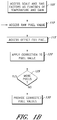
- Figure 1B is a flowchart that illustrates an example method for processing an image or output from a sensor using an implementation of the correction model described with reference to Equations (1) and (2).
- the example method can be implemented by the image processing system.
- the method accesses the scale and bias factors, scale(G,T) and bias(G,T), for the gain and temperature of the sensor.
- the method accesses a raw pixel value raw(x,y,G,T) for a pixel at location x and y on the sensor.
- the sensor can include (or be coupled with) a temperature sensor that determines the temperature T, and the sensor electronics can output the gain G applied to the sensor.
- the method accesses the offset value offset(x,y) for the location x and y on the sensor.
- the corrected pixel value p(x,y,G,T) is calculated using, for example, Equation (2).
- the method returns to block 110. If there are no additional pixels to process, the method continues at block 130 and provides the corrected pixel values p(x,y,G,T), for example, by storing them in a computer-readable medium or communicating them to an electronic component or user of the image processing system. Accordingly, the example method utilizes a single offset value at each pixel together with global (e.g., one value across the pixel array) temperature and gain dependent scale and bias terms.
- the scale and bias factors can vary across the sensor array. For example, groups of pixels (e.g., quadrants or other portions of the sensor) may be corrected with a scale and/or bias factor that is determined to apply to that particular group of pixels. Accordingly, Equations (1) or (2) may be applied to individual pixels within a portion of the sensor array such that the scale and/or bias factors are individually determined for each specific portion of the array. Many variations are possible.
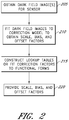
- Figure 2 is a flowchart that illustrates an example method for determining the correction terms scale(G,T), bias(G,T), and offset(x,y).
- the example method can be implemented by the image processing system discussed above or by a sensor calibration system comprising non-transitory computer storage and a hardware computer processor.
- one or more dark field images are taken with the sensor. Although one dark field image can be used, multiple dark field images may provide increased signal to noise and a better estimate of the sensor dark current than a single dark field image.
- the raw pixel values of the dark field images can be averaged to provide an average dark current value for each pixel as a function of gain and temperature, darkav(x,y,G,T).
- the dark field image(s) can be obtained at one or more gain values (G dim values) and/or one or more temperature values (T dim values) over the operating ranges for gain and temperature.
- the method obtains the average dark field values by accessing dark field image(s) stored on computer storage.
- bad pixels on the sensor can be identified and not used in the calculations for the correction model parameters. For example, pixels in the averaged dark field image that exceed a given threshold can be flagged as "bad". The union of such pixels for all temperatures and gains can be used as a bad pixel mask. In some of the results described herein, the threshold was 100, which pruned approximately 0.5 percent of the pixels on the tested sensor. In other implementations, bad pixels can be identified using a collection of multiple bright field images. The pixels that deviate more than some number of standard deviations from the mean pixel value can be marked as bad.
- the average dark current values for the sensor are fit to the correction model (e.g., Eq. (1)) to determine the parameters of the correction model: scale(G,T), bias(G,T), and offset(x,y).
- the correction model e.g., Eq. (1)
- statistical regression techniques can be used to fit the correction model to the average dark current.
- an objective function is defined and numerical methods are used to reduce or minimize the objective function to determine "best-fit" values for scale(G,T), bias(G,T), and offset(x,y).
- the objective function may be the sum over a group of pixels in the array of the squared error: error 2 ( x,y,G,T ) .
- the objective function is reduced or minimized over smaller patches of the pixel array to determine the correction terms, and then these correction terms are averaged. For example, for certain sensors, 40 dark field images were taken at each temperature and gain. The correction terms were fit over 20x20 patches of the resulting averaged dark field image. In this case, there are 20*20 + 2 * G dim * T dim unknown parameters to fit. For example, if G dim is 2 and T dim is 7, there would be 428 unknown parameters. Note that this is much less than the 5600 unknown parameters that would be needed if individual correction factors for each pixel were used.
- An iterative numerical solver can be used to determine these parameters. This procedure can be repeated for multiple different patches of the dark field image, and the results averaged. In some such cases, eight 20x20 patches were used on the top half of the dark field image and eight 20x20 patches were used on the bottom half of the dark field image. The results for the top half and the bottom half of the image can be averaged to provide an overall estimate for scale(G,T) and bias(G,T).
- bad sensor pixels can be identified (e.g., via the threshold techniques) and removed from the calculations for the correction model parameters.
- a lower threshold is first used so that a relatively larger proportion of bad pixels are identified, for example, 1%, 2%, 5%, 7%, 10%, or more of the pixels.
- the scale(G,T) and bias(G,T) factors can then be determined from the resulting set of "good" pixels, which can reduce the errors in the determination of these factors as compared to using sensor data sets that include more bad pixels.
- the threshold can then be increased (e.g., to the levels described above) so that fewer bad pixels are identified (e.g., less than 0.5% or 1% of the pixels), and the offset(x,y) factor determined for this larger set of pixels.
- Some implementations of the method at block 215 construct lookup tables and/or fit functional forms to one or more of scale(G,T), bias(G,T), and offset(x,y).
- scale(G,T), bias(G,T), and offset(x,y) can be provided, for example, by storing them in a computer-readable medium or communicating them to an electronic component or user of the image processing system or a sensor calibration system.
- embodiments of the method described with reference to Figure 2 can provide an optimized solution for pixel offsets and temperature and gain indexed global scale and biases.
- a non-linear solver can be used fit a correction model to multiple dark field images collected over a desired operating temperature range and a desired operating gain range.
- the non-linear solver optimizes an objective function based at least partly on the squared difference between the dark field images and the correction model.
- the solver can be applied to a subset of the image pixels to derive the scale and bias terms. Once these are derived, the offset values of all the pixels can be determined from the scale and bias terms and the dark field image values.
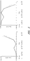
- Figure 3 includes graphs showing examples of scale(G,T) (on the left) and bias(G,T) (on the right).
- the vertical axis in each graph is scale or bias, respectively.
- the horizontal axis shows curves for the two gain values (2x and 10x) at each of the temperature values between 0.8 C and 73 C.
- the lighter dashed curves show eight solutions solved on different 20x20 pixel patches on the sensor, and the heavy solid curve shows the average of these eight solutions.
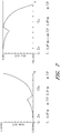
- Figure 4 shows graphs of examples of model fit error using LUTs generated with all temperature data from 0.8 through 73 degrees centigrade.
- the upper graph shows the standard deviation of dark field pixel fit error at each temperature and gain setting (2x and 10x).
- the overall standard deviation of the dark field pixel fit error is about 2.58 in this example.
- the lower graph shows fit error histograms for each temperature and gain setting.
- the dark field data for a subset of the temperatures was used for determining scale(G,T), bias(G,T), and offset(x,y).
- data for three temperatures was used: 0.8 C, 37 C, and 73 C to determine scale(G,T), bias(G,T), and offset(x,y), and these fits were used to estimate dark offset images for the remaining temperatures (12 C, 24 C, 48 C, and 60 C).
- a dark field bad pixel threshold of 520 was used for this data, which resulted in 1% of the pixels being marked bad.
- Figures 5 and 6 show examples that are generally similar to Figures 3 and 4 , respectively, described above, except that the gain, bias, and offsets were determined from data for three temperatures: 0.8 C, 37 C, and 73 C.
- the overall standard deviation of the dark field pixel fit error is about 6.30 in this example.
- the scale and bias terms may be relatively similar in value and shape for different sensors of the same type. Accordingly, the scale and bias terms can be evaluated for one particular sensor, and then the same scale and bias terms used for other sensors of the same type. In some such implementations, only the pixel-dependent offset values would be determined for each particular sensor.
- the offset values can be determined using a reduced set of calibration data, for example, dark field images taken using 2x and 10x gains and at a single temperature (e.g., the high end of the operating temperature range). Further, the offset can readily be determined from Equation (5) using scale, bias, and darkav from the reduced set of calibration data.
- Figures 7 and 8 show examples that are generally similar to the examples shown in Figures 3 and 4 , respectively, described above.
- the results shown in Figures 7 and 8 are somewhat better than the example using three temperatures in Section B described above (see, e.g., Figs. 5 and 6 ).
- the overall standard deviation of the dark field pixel fit error is about 3.64 in this example, whereas the standard deviation of the fit error is about 6.30 in the three-temperature example in Section B.
- the scale and bias versus temperature curves may be generally similar for different sensors of the same type, and the scale and bias curves can be reused when calibrating new sensors. While the derivation of the original scale and bias curves can be computationally demanding, embodiments of this method can use the determined scale and bias terms and Equation (5) to determine the pixel-dependent offset for new sensors. Accordingly, determination of the correction model for new sensors advantageously can be performed computationally efficiently.
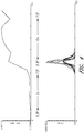
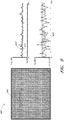
- Figure 9 shows an example of a dark image 900 and comparisons of pixel offset values against raw pixel values from a 100 pixel-long slice 905 through the dark image 900 in the graphs on the right.
- Trace 910 shows a model estimated for the pixel dark current values using the techniques described herein, and trace 915 shows the raw pixel values along the slice 905.
- Trace 920 in the lower graph shows the difference between the model estimates 910 and the raw pixel values 915.
- Figures 10 and 11 show example dark images 1000, 1100, respectively.
- the dark images 1000, 1100 include 100 pixel-long slices 1005, 1105 shown as horizontal bars in the upper half of the dark images 1000, 1100, respectively.
- Figures 10 and 11 are for two different data sets.
- Figures 10 and 11 also include graphs showing overlayed traces 1015, 1115, respectively, of data from the 100 pixel-long slices 1005, 1105, respectively, for all temperatures and gains.
- each pixel can have a rather complex operational behavior that may depend on one or more factors including number of photons collected by the pixel, temperature, gain settings, and physical or manufacturing variations. Accordingly, embodiments of the systems and methods described herein can be used to calibrate each pixel to produce a substantially uniform behavior across the sensor with regard to the relationship between photon collection and output signal. For example, in some embodiments, calibration can be thought of as building a model for each pixel that describes the variation among pixels in a way that allows removing the influence of those variations on the desired output.
- the calibration uses information stored in a computer-readable memory (e.g., scale, bias, and offset factors), and there can be a tradeoff between storing greater amounts of information (which may increase quality of the calibration) and the costs of increased memory storage for the information and/or the processing power and time needed to perform the calibration.
- information stored in a computer-readable memory e.g., scale, bias, and offset factors
- the calibration (for at least a subset of sensor pixels) is factored into two parts: (1) one or more global calibration factors that apply to all pixels of the subset uniformly and (2) a specific calibration that applies to each pixel in the subset individually.
- dark current correction can be performed using (1) global scale and bias functions that depend on temperature and/or gain, and (2) local offset values for each pixel.
- the offset value for a pixel can be derived to provide an improved or "best" solution for the pixel based at least partly on the choice of scale and bias functions.
- the choice of scale and bias functions can be provided to give an increased ability to select offset values that work well.
- optimization techniques can be used to derive an efficient factorization of the calibration into global and local components.
- Embodiments of such techniques can be applied to dark current correction as well as to other aspects of pixel calibration such as, e.g., correcting for uniformity of performance across the range of light exposure levels.
- two global factors and one offset factor are utilized.
- the number of global factors and/or the number of local factors can be one, two, three, or more.
- the calibration is factored into local and global components to improve calibration performance for a given resource allocation.
- optimization techniques can be used to obtain the factorization into local and global components.
- Embodiments of the systems and methods described herein can access the global and/or local factor(s) from a computer-readable memory that stores the factor(s) as data structures (e.g., LUTs, databases, etc.), mathematical functions (e.g., splines, polynomials, etc.), and so forth.
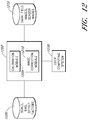
- FIG 12 is a block diagram that schematically illustrates an example implementation of a system 1200 for calibrating sensors and correcting images for the effects of dark current.
- dark field images obtained from a sensor can be stored in a physical data repository 1215.
- a dark current analysis engine 1202 can include a calibration module 1205 for determining a calibration for the sensor that will correct for the effects of dark current.
- the calibration module 1205 can implement the method described with reference to Figure 2 to determine global and/or local factors (e.g., scale, bias, and offset factors) that correct for dark current. These correction factors can be stored in a physical data repository 1220.
- the dark current analysis engine 1202 can also include an image correction module 1210 that accesses sensor images stored in the data repository 1215, applies the correction factors stored in the data repository 1220 to the sensor images, to determine a sensor image corrected for dark current.
- the image correction module 1210 can implement the method described with reference to Figure IB.
- the dark current analysis engine 1202 can store the corrected sensor image in the data repository 1215.
- the engine 1202 can communicate the corrected image to a user.
- a user computing system 1230 can communicate a sensor image to the image correction module 1210, which can apply the correction factors from the data repository 1220, and return a corrected sensor image to the user computing system 1230.
- the dark current analysis engine 1202 can be implemented on physical computing hardware.
- the system 1200 is intended to be illustrative and not limiting. In other implementations, the functionalities and/or components of the system 1200 can be arranged differently than shown in Figure 12 .
- the repositories 1215 and 1220 can be merged together or separated into additional repositories.
- the engine 1202 may be configured so that the calibration module 1205 and the image correction module 1210 are implemented on separate computing systems. For example, sensor calibration may be performed by a first computing system and image correction may be performed by a different computing system. Many variations are possible.
- Embodiments of the sensors, systems, and methods described herein can be used in any type of electronic imaging system or to process image data received from an imaging sensor.
- the sensors, systems, and methods can be used with a geo-imaging system in an Earth-orbiting satellite or micro-satellite.
- the sensors, systems, and methods can be used with cameras in cellular telephones.
- Each of the processes, methods, and algorithms described herein and/or depicted in the attached figures may be embodied in, and fully or partially automated by, code modules executed by one or more physical computing systems, computer processors, application-specific circuitry, and/or electronic hardware configured to execute computer instructions.
- computing systems can include general or special purpose computers, servers, desktop computers, laptop or notebook computers or tablets, personal mobile computing devices, mobile telephones, and so forth.
- a code module may be compiled and linked into an executable program, installed in a dynamic link library, or may be written in an interpreted programming language.
- Code modules may be stored on any type of non-transitory computer-readable medium, such as physical computer storage including hard drives, solid state memory, random access memory (RAM), read only memory (ROM), optical disc, volatile or non-volatile storage, combinations of the same and/or the like.
- the methods and modules may also be transmitted as generated data signals (e.g., as part of a carrier wave or other analog or digital propagated signal) on a variety of computer-readable transmission mediums, including wireless-based and wired/cable-based mediums, and may take a variety of forms (e.g., as part of a single or multiplexed analog signal, or as multiple discrete digital packets or frames).
- the results of the disclosed processes and process steps may be stored, persistently or otherwise, in any type of non-transitory, tangible computer storage or may be communicated via a computer-readable transmission medium.
- any processes, blocks, states, steps, or functionalities in flow diagrams described herein and/or depicted in the attached figures should be understood as potentially representing code modules, segments, or portions of code which include one or more executable instructions for implementing specific functions (e.g., logical or arithmetical) or steps in the process.
- the various processes, blocks, states, steps, or functionalities can be combined, rearranged, added to, deleted from, modified, or otherwise changed from the illustrative examples provided herein.
- additional or different computing systems or code modules may perform some or all of the functionalities described herein.
- the processes, methods, and systems may be implemented in a network (or distributed) computing environment.
- Network environments include enterprise-wide computer networks, intranets, local area networks (LAN), wide area networks (WAN), cloud computing networks, crowd-sourced computing networks, the Internet, and the World Wide Web.
- the network may be a wired or a wireless network (e.g., a terrestrial and/or satellite network) or any other type of communication network.
- any reference to “one embodiment” or “some embodiments” or “an embodiment” means that a particular element, feature, structure, or characteristic described in connection with the embodiment is included in at least one embodiment.
- the appearances of the phrase “in one embodiment” in various places in the specification are not necessarily all referring to the same embodiment.
- Conditional language used herein, such as, among others, “can,” “could,” “might,” “may,” “e.g.,” and the like, unless specifically stated otherwise, or otherwise understood within the context as used, is generally intended to convey that certain embodiments include, while other embodiments do not include, certain features, elements and/or steps.
- the terms “comprises,” “comprising,” “includes,” “including,” “has,” “having” or any other variation thereof, are open-ended terms and intended to cover a non-exclusive inclusion.
- a process, method, article, or apparatus that comprises a list of elements is not necessarily limited to only those elements but may include other elements not expressly listed or inherent to such process, method, article, or apparatus.
- "or" refers to an inclusive or and not to an exclusive or.
- a condition A or B is satisfied by any one of the following: A is true (or present) and B is false (or not present), A is false (or not present) and B is true (or present), and both A and B are true (or present).
- a phrase referring to "at least one of' a list of items refers to any combination of those items, including single members.
- "at least one of: A, B, or C” is intended to cover: A, B, C, A and B, A and C, B and C, and A, B, and C.
- Conjunctive language such as the phrase "at least one of X, Y and Z," unless specifically stated otherwise, is otherwise understood with the context as used in general to convey that an item, term, etc. may be at least one of X, Y or Z. Thus, such conjunctive language is not generally intended to imply that certain embodiments require at least one of X, at least one of Y and at least one of Z to each be present.
Landscapes
- Engineering & Computer Science (AREA)
- Multimedia (AREA)
- Signal Processing (AREA)
- Transforming Light Signals Into Electric Signals (AREA)
Description
- The present disclosure relates generally to calibrating sensors such as, for example, photosensors, which have pixel-dependent noise or bias.
- Photosensors can be used to detect the amount of light incident on the image sensor. Photosensors include, for example, devices such as charge-coupled devices (CCDs) in which each pixel includes a photoactive capacitor, and active pixel image sensors in which each pixel includes a light sensor and an active amplifier. The amplifier can provide a programmable or switchable gain for each pixel. Active pixel image sensors produced by complementary metal-oxide-semiconductor (CMOS) techniques are commonly known as CMOS sensors. Generally, the amount of electric current produced by a pixel of the photosensor increases with the amount of light incident on the pixel. However, even when no light is incident on the pixel, a small amount of electric current, commonly called "dark current," can flow from the pixel. When an image is taken with a photosensor, dark current can act as a source of noise in the resulting image. Dark current noise can be reduced by using dark-frame subtraction in which a dark field image, taken with little or no light incident on the sensor, is subtracted from the image to at least partially compensate for the noise produced by the dark current.
-
- Throughout the drawings, reference numbers may be re-used to indicate correspondence between referenced elements. The drawings are provided to illustrate example embodiments described herein and are not intended to limit the scope of the disclosure.
-
Figure 1A schematically illustrates an example of a two-dimensional photosensor that includes electronics to apply a gain G to the sensor and to measure (and/or control) the temperature T of the sensor. - Figure IB is a flowchart that illustrates an example method for processing an image or output from a photosensor using an implementation of a correction model described herein.
-
Figure 2 is a flowchart that illustrates an example method for determining correction terms for scale, bias, and offset factors for one example implementation of the correction model. -
Figure 3 includes graphs showing examples of scale factors (on the left) and bias factors (on the right) as a function of sensor gain (two times gain (2x) and ten times gain (10x)) and sensor temperature from 0.8 through 73 degrees centigrade. -
Figure 4 shows graphs of examples of model fit error using for temperature data from 0.8 through 73 degrees centigrade. The upper graph shows an example of the standard deviation of dark field pixel fit error at each temperature and gain setting (2x and 10x). The lower graph shows fit error histograms for each temperature and gain setting. -
Figure 5 includes graphs showing additional examples of scale factors (on the left) and bias factors (on the right) as a function of sensor gain (2x and 10x) and sensor temperature from 0.8 through 73 degrees centigrade. -
Figure 6 shows graphs of additional examples of model fit error using for temperature data from 0.8 through 73 degrees centigrade. The upper graph shows another example of the standard deviation of dark field pixel fit error at each temperature and gain setting (2x and 10x). The lower graph shows fit error histograms for each temperature and gain setting. -
Figure 7 includes graphs showing an additional example of a scale factor (on the left) and a bias factor (on the right) as a function of sensor gain (2x and 10x) and sensor temperature from 0.8 through 73 degrees centigrade. -
Figure 8 shows graphs of additional examples of model fit error using for temperature data from 0.8 through 73 degrees centigrade. The upper graph shows another example of the standard deviation of dark field pixel fit error at each temperature and gain setting (2x and 10x). The lower graph shows fit error histograms for each temperature and gain setting. -
Figure 9 shows an example of a dark image (on the left) and comparisons of pixel offset values against raw pixel values from a 100 pixel-long slice through the dark image in the graphs on the right. -
Figure 10 shows another example of a dark image (on the left) and comparisons of pixel offset values against raw pixel values from a 100 pixel-long slice through the dark image in the graph on the right. -
Figure 11 shows another example of a dark image (on the left) and comparisons of pixel offset values against raw pixel values from a 100 pixel-long slice through the dark image in the graph on the right. -
Figure 12 is a block diagram that schematically illustrates an implementation of a system for calibrating photosensors and correcting images for dark current. - In a first aspect of the invention, a computer implemented method of correcting for dark current in a photosensor comprising a plurality of pixels is presented by claim 1, and a system for correcting for dark current in a sensor comprising a plurality of pixels is presented by claim 8.
- Optional features are set out in the dependent claims.
- As discussed, dark current can depend, among other factors, on the temperature of the sensor (and/or the gain applied to the sensor). Some implementations of an imaging device may include a temperature controller configured to adjust or control the temperature of the sensor. Because the sensor is kept at a controlled temperature, the dark current need not be corrected for variations in temperature of the sensor. However, temperature controllers often use significant amounts of power, and thus may not be used in certain implementations such as low-power implementations, satellite implementations, and so forth. In some of these implementations, the temperature of the sensor may vary during operation, and it may be desirable to correct for temperature-dependent effects of the dark current. Thus, a temperature sensor can be used to measure the temperature of the sensor. The disclosure herein provides examples of systems and methods for correcting for temperature-dependent effects of the dark current based on a measured or inferred temperature of the sensor. As will be further described herein, these methods can also be used to correct for gain-dependent effects of the dark current.
- Embodiments of the systems and methods disclosed herein may be advantageously used for sensors that operate in low-power conditions or in space (e.g., satellites or micro-satellites), or in applications where a sensor temperature-controller is not used. For example, embodiments of the systems and methods can be used for sensors incorporated in mobile telephones, portable or desktop computers or tablets, etc.
- The following illustrative examples will be described in the context of a photosensor. As used herein, photosensor is a broad term and is to be given its ordinary and customary meaning to a person of ordinary skill in the art (e.g., it is not to be limited to a special or customized meaning). Photosensors include, but are not limited to, image sensors, light sensors, optical sensors, active pixel sensors, charge-coupled devices, photodetectors, photodiodes, photoresistors, photoelectric devices, or other optoelectronic devices. Photosensors can be configured to be sensitive to visible light (e.g., having wavelengths in a range from about 400 nm to about 800 nm) and/or non-visible light (e.g., having wavelengths outside the visible range, such as X-ray, ultraviolet, or infrared wavelengths). In some implementations, a photosensor can be sensitive to a panchromatic range of wavelengths such as, e.g., visible wavelengths and near-infrared wavelengths.
- The photosensor can include an array of pixels. Individual pixels in the array can be identified by an x index and y index. Each index can run from 1 to the total number of pixels in the x or y direction of the array. For example, for a square array of pixels, the x and y indices can run from 1 to N, where N is the number of pixels in each direction of the pixel array. In some cases, N can be in the range from 10 to 1000 or greater. For example, a sensor can be configured as an 80x80 array of pixels. Other pixel arrangements are possible. For example, the sensor can be a rectangular two-dimensional array of N x M pixels (e.g., a non-square array with N ≠ M). As another example, the sensor can be a one-dimensional array of pixels, which may be referred to as an N x 1 array.
- Each pixel (at location x, y in the sensor array) can output a value (typically a voltage or a current) that can depend on factors such as, e.g., sensor temperature T and sensor gain G.
Figure 1A schematically illustrates an example of a two-dimensional sensor 100 having an array of pixels (e.g., pixel 101). Thesensor 100 can includeelectronics 102 to apply the gain G to thesensor 100 and to measure (and/or control) the temperature T of thesensor 100. - In response to receiving incident light, each pixel of the sensor can output a pixel value that is generally proportional to the amount of incident light received by the pixel. The raw pixel value also includes noise sources including dark current. In the following illustrative model, the raw pixel value from the sensor pixel at position (x,y) in the sensor array will be denoted by raw(x,y,G,T), and the pixel value corrected for dark current will be denoted by p(x,y,G,T). To correct each raw pixel value for sensor temperature T and gain G, a pixel-dependent correction c(x,y,G,T) can be applied to the raw pixel output raw(x,y,G,T) (e.g., by subtracting the correction c(x,y,G,T) from the raw pixel value raw(x,y,G,T) to determine the corrected pixel value p(x,y,G,T), e.g., p(x,y,G,T) = raw(x,y,G,T) - c(x,y,G,T)). However, some such methods can consume a significant amount of memory in the processing system that performs the correction. For example, if the gain is discretized over Gdim gain values, and the temperature is discretized over Tdim temperature values, the number of independent values for the pixel-dependent correction c(x,y,G,T) for an N x N sensor can be N2 * Gdim * Tdim, which can be quite large for large format sensor arrays.
- Accordingly, in some implementations, the pixel-dependent correction can be modeled as (1) a global scale factor, (2) a global bias that depends on temperature and gain, and (3) a temperature-independent and gain-independent offset value for each pixel. In some such implementations, the global scale factor and the global bias can depend on gain and temperature and will be denoted by scale(G,T) and bias(G,T), respectively. The offset value for each pixel will be denoted by offset(x,y). In some such implementations, the correction factor can be written as

- An individual pixel value can be determined using Equation (1) as:

- In some implementations, an image processing system comprising computer storage and a hardware processor can access the raw pixel values (e.g., directly from the photosensor or from a stored image) and apply the corrections using Equation (2). The scale and bias factors can be stored as lookup tables (LUTs) (or other suitable data structures) indexed by gain and temperature. Interpolation or extrapolation methods can be used for values of gain or temperatures that do not fall precisely on an indexed gain or temperature value, respectively. In some cases, the scale and bias factors may be fit as one or more mathematical functions of G and T, for example, as polynomials, splines, etc. In various embodiments, the offset can be stored as a two-dimensional LUT or fit as one or more mathematical functions of index values x and y (e.g., splines, polynomials, etc.). Accordingly, in certain such implementations, the systems and methods may determine or evaluate an LUT or fitting function for one or more of the scale factor, bias factor, and/or the offset factors. In various embodiments, each pixel can be processed serially or a group of some or all of the pixels can be processed in parallel fashion.
- In some example implementations, not according to the invention, in addition to depending on temperature and/or gain, the scale and/or bias factors may have values that are different for different groups of pixels in the sensor. For example, scale and/or bias factors may be determined for groups of pixels that are identified as having similar gain and/or temperature dependency. As another example, scale and/or bias factors can be determined for different physical regions of the sensor (e.g., scale factors and/or bias factors can be determined for each of the four quadrants of the sensor). Thus, in some such implementations, not according to the invention, there may be a plurality of scale and/or bias factors that are applied to different groups of pixels in the sensor. As an example, if the sensor includes Kdim different groups of pixels, the plurality of scale and/or bias factors may be written as scalek (G,T) and biask (G,T), where k = 1,...,Kdim indexes the different groups of pixels. The correction factor can be written as:

- In some implementations, not according to the invention there may be individual scale and/or bias factors for each pixel of the sensor such that these factors can be alternatively be written as scale(G,T) and/or bias(x,y,G,T) (e.g., Kdim = N2 in this example). The number of scale and/or bias factors selected for use with a particular sensor may depend at least partly on considerations including processing power and/or memory size of the imaging system electronics. For example, increased processing power and/or memory size may permit use of an increased value for Kdim. Use of larger values of Kdim may in some cases provide a more accurate correction factor c(x,y,G,T) for the sensor since the scale and/or bias factors can account for variations across the sensor. Accordingly, in some such cases, a further consideration for selecting the number of scale and/or bias factors may be a tradeoff between accuracy (e.g., use of larger Kdim) and image processing speed (e.g., use of smaller Kdim).
-
Figure 1B is a flowchart that illustrates an example method for processing an image or output from a sensor using an implementation of the correction model described with reference to Equations (1) and (2). The example method can be implemented by the image processing system. Atblock 105, the method accesses the scale and bias factors, scale(G,T) and bias(G,T), for the gain and temperature of the sensor. Atblock 110, the method accesses a raw pixel value raw(x,y,G,T) for a pixel at location x and y on the sensor. The sensor can include (or be coupled with) a temperature sensor that determines the temperature T, and the sensor electronics can output the gain G applied to the sensor. Atblock 115, the method accesses the offset value offset(x,y) for the location x and y on the sensor. Atblock 120, the corrected pixel value p(x,y,G,T) is calculated using, for example, Equation (2). Atblock 125, if there are additional pixels to process, the method returns to block 110. If there are no additional pixels to process, the method continues atblock 130 and provides the corrected pixel values p(x,y,G,T), for example, by storing them in a computer-readable medium or communicating them to an electronic component or user of the image processing system. Accordingly, the example method utilizes a single offset value at each pixel together with global (e.g., one value across the pixel array) temperature and gain dependent scale and bias terms. - In other implementations, not according to the invention, rather than correcting for both gain and temperature, only one of these parameters is corrected for by the example method of Figure IB. In yet other implementations, not according to the invention, the scale and bias factors can vary across the sensor array. For example, groups of pixels (e.g., quadrants or other portions of the sensor) may be corrected with a scale and/or bias factor that is determined to apply to that particular group of pixels. Accordingly, Equations (1) or (2) may be applied to individual pixels within a portion of the sensor array such that the scale and/or bias factors are individually determined for each specific portion of the array. Many variations are possible.
-
Figure 2 is a flowchart that illustrates an example method for determining the correction terms scale(G,T), bias(G,T), and offset(x,y). The example method can be implemented by the image processing system discussed above or by a sensor calibration system comprising non-transitory computer storage and a hardware computer processor. - At
block 205, one or more dark field images are taken with the sensor. Although one dark field image can be used, multiple dark field images may provide increased signal to noise and a better estimate of the sensor dark current than a single dark field image. The raw pixel values of the dark field images can be averaged to provide an average dark current value for each pixel as a function of gain and temperature, darkav(x,y,G,T). The dark field image(s) can be obtained at one or more gain values (Gdim values) and/or one or more temperature values (Tdim values) over the operating ranges for gain and temperature. In some cases, the method obtains the average dark field values by accessing dark field image(s) stored on computer storage. - In some implementations, bad pixels on the sensor can be identified and not used in the calculations for the correction model parameters. For example, pixels in the averaged dark field image that exceed a given threshold can be flagged as "bad". The union of such pixels for all temperatures and gains can be used as a bad pixel mask. In some of the results described herein, the threshold was 100, which pruned approximately 0.5 percent of the pixels on the tested sensor. In other implementations, bad pixels can be identified using a collection of multiple bright field images. The pixels that deviate more than some number of standard deviations from the mean pixel value can be marked as bad.
- At
block 210, the average dark current values for the sensor are fit to the correction model (e.g., Eq. (1)) to determine the parameters of the correction model: scale(G,T), bias(G,T), and offset(x,y). For example, statistical regression techniques can be used to fit the correction model to the average dark current. In some implementations ofblock 210, an objective function is defined and numerical methods are used to reduce or minimize the objective function to determine "best-fit" values for scale(G,T), bias(G,T), and offset(x,y). For example, the "error" at each pixel can be defined as
- The objective function may be the sum over a group of pixels in the array of the squared error: error2 (x,y,G,T). In some such implementations, the objective function is reduced or minimized over smaller patches of the pixel array to determine the correction terms, and then these correction terms are averaged. For example, for certain sensors, 40 dark field images were taken at each temperature and gain. The correction terms were fit over 20x20 patches of the resulting averaged dark field image. In this case, there are 20*20 + 2 * Gdim * Tdim unknown parameters to fit. For example, if Gdim is 2 and Tdim is 7, there would be 428 unknown parameters. Note that this is much less than the 5600 unknown parameters that would be needed if individual correction factors for each pixel were used.
- An iterative numerical solver can be used to determine these parameters. This procedure can be repeated for multiple different patches of the dark field image, and the results averaged. In some such cases, eight 20x20 patches were used on the top half of the dark field image and eight 20x20 patches were used on the bottom half of the dark field image. The results for the top half and the bottom half of the image can be averaged to provide an overall estimate for scale(G,T) and bias(G,T).
- In some implementations, the averaged values for scale(G,T) and bias(G,T) can be used to solve for offset values at each pixel in the full dark image as:

- In some cases, including bad sensor pixels in the determination of the scale(G,T), and bias(G,T) factors can lead to errors in these factors. Accordingly, as discussed above bad sensor pixels can be identified (e.g., via the threshold techniques) and removed from the calculations for the correction model parameters. In some such cases, a lower threshold is first used so that a relatively larger proportion of bad pixels are identified, for example, 1%, 2%, 5%, 7%, 10%, or more of the pixels. The scale(G,T) and bias(G,T) factors can then be determined from the resulting set of "good" pixels, which can reduce the errors in the determination of these factors as compared to using sensor data sets that include more bad pixels. The threshold can then be increased (e.g., to the levels described above) so that fewer bad pixels are identified (e.g., less than 0.5% or 1% of the pixels), and the offset(x,y) factor determined for this larger set of pixels. Some such methods advantageously can provide better determinations of the scale(G,T) and bias(G,T) factors, while also providing offset(x,y) values for a larger number of pixels.
- Some implementations of the method at
block 215 construct lookup tables and/or fit functional forms to one or more of scale(G,T), bias(G,T), and offset(x,y). Atblock 220, scale(G,T), bias(G,T), and offset(x,y) (or the associated LUTs or functional fits) can be provided, for example, by storing them in a computer-readable medium or communicating them to an electronic component or user of the image processing system or a sensor calibration system. - Accordingly, embodiments of the method described with reference to
Figure 2 can provide an optimized solution for pixel offsets and temperature and gain indexed global scale and biases. A non-linear solver can be used fit a correction model to multiple dark field images collected over a desired operating temperature range and a desired operating gain range. In some cases, the non-linear solver optimizes an objective function based at least partly on the squared difference between the dark field images and the correction model. The solver can be applied to a subset of the image pixels to derive the scale and bias terms. Once these are derived, the offset values of all the pixels can be determined from the scale and bias terms and the dark field image values. - An implementation of the method described with reference to
Figure 2 was used to determine scale(G,T), bias(G,T), and offset(x,y) for a CMOS photosensor. Example results are described below. In these examples, the analog gain of the sensor could be 2-times (2x) or ten-times (10x). The temperature values (in degrees centigrade) included 0.8 C, 12 C, 24 C, 37 C, 48 C, 60 C, and 73 C. Thus, Gdim is 2 and Tdim is 7 in some of the example results below. In other example, other numbers of gains and temperature values can be used, e.g., Gdim can be 1, 3, 4, 5, 6, or more and/or Tdim can be 1, 2, 3, 4, 5, 6, 8, 9, 10, or more. As further discussed herein, pixel correction may be implemented for only one of gain or temperature, rather than both gain and temperature, or may be implemented for corrections of variables in addition or as an alternative to gain and/or temperature. - In this example, a dark field bad pixel threshold of 520 was used, which resulted in about 1% of the pixels being marked bad.
Figure 3 includes graphs showing examples of scale(G,T) (on the left) and bias(G,T) (on the right). The vertical axis in each graph is scale or bias, respectively. The horizontal axis shows curves for the two gain values (2x and 10x) at each of the temperature values between 0.8 C and 73 C. The lighter dashed curves show eight solutions solved on different 20x20 pixel patches on the sensor, and the heavy solid curve shows the average of these eight solutions. - As can be seen from
Figure 3 , in this example the absolute magnitude of both scale and bias increase as temperature increases. Also, for the same temperature, the absolute magnitude of both scale and bias are larger for larger gain. -
Figure 4 shows graphs of examples of model fit error using LUTs generated with all temperature data from 0.8 through 73 degrees centigrade. The upper graph shows the standard deviation of dark field pixel fit error at each temperature and gain setting (2x and 10x). The overall standard deviation of the dark field pixel fit error is about 2.58 in this example. The lower graph shows fit error histograms for each temperature and gain setting. - In this example, the dark field data for a subset of the temperatures was used for determining scale(G,T), bias(G,T), and offset(x,y). In this example, data for three temperatures was used: 0.8 C, 37 C, and 73 C to determine scale(G,T), bias(G,T), and offset(x,y), and these fits were used to estimate dark offset images for the remaining temperatures (12 C, 24 C, 48 C, and 60 C). A dark field bad pixel threshold of 520 was used for this data, which resulted in 1% of the pixels being marked bad.
-
Figures 5 and6 show examples that are generally similar toFigures 3 and4 , respectively, described above, except that the gain, bias, and offsets were determined from data for three temperatures: 0.8 C, 37 C, and 73 C. The overall standard deviation of the dark field pixel fit error is about 6.30 in this example. - The example results presented in
Figures 5 and6 demonstrate that a subset of the temperatures in the range of operating temperatures for the device can be used to determine the correction model terms scale(G,T), bias(G,T), and offset(x,y). Likewise, it is believed that a subset of gains in the range of gains could be used to determine the correction model terms. Accordingly, certain embodiments advantageously may use only a subset of the Gdim gains and the Tdim temperatures to determine scale(G,T), bias(G,T), and offset(x,y). - For some types of sensors, the scale and bias terms may be relatively similar in value and shape for different sensors of the same type. Accordingly, the scale and bias terms can be evaluated for one particular sensor, and then the same scale and bias terms used for other sensors of the same type. In some such implementations, only the pixel-dependent offset values would be determined for each particular sensor. The offset values can be determined using a reduced set of calibration data, for example, dark field images taken using 2x and 10x gains and at a single temperature (e.g., the high end of the operating temperature range). Further, the offset can readily be determined from Equation (5) using scale, bias, and darkav from the reduced set of calibration data.
- In the following example, dark field image data at a temperature of 73 C was used to derive offset(x,y).
Figures 7 and8 show examples that are generally similar to the examples shown inFigures 3 and4 , respectively, described above. The results shown inFigures 7 and8 are somewhat better than the example using three temperatures in Section B described above (see, e.g.,Figs. 5 and6 ). For example, the overall standard deviation of the dark field pixel fit error is about 3.64 in this example, whereas the standard deviation of the fit error is about 6.30 in the three-temperature example in Section B. - Accordingly, in some implementations, the scale and bias versus temperature curves may be generally similar for different sensors of the same type, and the scale and bias curves can be reused when calibrating new sensors. While the derivation of the original scale and bias curves can be computationally demanding, embodiments of this method can use the determined scale and bias terms and Equation (5) to determine the pixel-dependent offset for new sensors. Accordingly, determination of the correction model for new sensors advantageously can be performed computationally efficiently.
-
Figure 9 shows an example of adark image 900 and comparisons of pixel offset values against raw pixel values from a 100 pixel-long slice 905 through thedark image 900 in the graphs on the right.Trace 910 shows a model estimated for the pixel dark current values using the techniques described herein, and trace 915 shows the raw pixel values along theslice 905.Trace 920 in the lower graph shows the difference between the model estimates 910 and the raw pixel values 915. -
Figures 10 and11 show exampledark images dark images long slices dark images Figures 10 and11 are for two different data sets.Figures 10 and11 also include graphs showing overlayed traces 1015, 1115, respectively, of data from the 100 pixel-long slices - In various sensor implementations, each pixel can have a rather complex operational behavior that may depend on one or more factors including number of photons collected by the pixel, temperature, gain settings, and physical or manufacturing variations. Accordingly, embodiments of the systems and methods described herein can be used to calibrate each pixel to produce a substantially uniform behavior across the sensor with regard to the relationship between photon collection and output signal. For example, in some embodiments, calibration can be thought of as building a model for each pixel that describes the variation among pixels in a way that allows removing the influence of those variations on the desired output. In some such embodiments, the calibration uses information stored in a computer-readable memory (e.g., scale, bias, and offset factors), and there can be a tradeoff between storing greater amounts of information (which may increase quality of the calibration) and the costs of increased memory storage for the information and/or the processing power and time needed to perform the calibration.
- Therefore, to increase the quality of calibration for a given amount of calibration information storage, in certain embodiments the calibration (for at least a subset of sensor pixels) is factored into two parts: (1) one or more global calibration factors that apply to all pixels of the subset uniformly and (2) a specific calibration that applies to each pixel in the subset individually. For example, dark current correction can be performed using (1) global scale and bias functions that depend on temperature and/or gain, and (2) local offset values for each pixel. In certain embodiments, the offset value for a pixel can be derived to provide an improved or "best" solution for the pixel based at least partly on the choice of scale and bias functions. In certain such embodiments, the choice of scale and bias functions can be provided to give an increased ability to select offset values that work well. Thus, in certain such embodiments optimization techniques can be used to derive an efficient factorization of the calibration into global and local components. Embodiments of such techniques can be applied to dark current correction as well as to other aspects of pixel calibration such as, e.g., correcting for uniformity of performance across the range of light exposure levels.
- In certain embodiments described herein, two global factors and one offset factor are utilized. However, this is not a limitation, and in other embodiments, the number of global factors and/or the number of local factors can be one, two, three, or more. Thus, in various implementations, the calibration is factored into local and global components to improve calibration performance for a given resource allocation. In various such implementations, optimization techniques can be used to obtain the factorization into local and global components. Embodiments of the systems and methods described herein can access the global and/or local factor(s) from a computer-readable memory that stores the factor(s) as data structures (e.g., LUTs, databases, etc.), mathematical functions (e.g., splines, polynomials, etc.), and so forth.
-
Figure 12 is a block diagram that schematically illustrates an example implementation of a system 1200 for calibrating sensors and correcting images for the effects of dark current. In this system 1200, dark field images obtained from a sensor can be stored in aphysical data repository 1215. A darkcurrent analysis engine 1202 can include acalibration module 1205 for determining a calibration for the sensor that will correct for the effects of dark current. For example, thecalibration module 1205 can implement the method described with reference toFigure 2 to determine global and/or local factors (e.g., scale, bias, and offset factors) that correct for dark current. These correction factors can be stored in aphysical data repository 1220. The darkcurrent analysis engine 1202 can also include animage correction module 1210 that accesses sensor images stored in thedata repository 1215, applies the correction factors stored in thedata repository 1220 to the sensor images, to determine a sensor image corrected for dark current. For example, theimage correction module 1210 can implement the method described with reference to Figure IB. The darkcurrent analysis engine 1202 can store the corrected sensor image in thedata repository 1215. In some implementations, theengine 1202 can communicate the corrected image to a user. In some implementations, auser computing system 1230 can communicate a sensor image to theimage correction module 1210, which can apply the correction factors from thedata repository 1220, and return a corrected sensor image to theuser computing system 1230. The darkcurrent analysis engine 1202 can be implemented on physical computing hardware. - The system 1200 is intended to be illustrative and not limiting. In other implementations, the functionalities and/or components of the system 1200 can be arranged differently than shown in
Figure 12 . For example, therepositories engine 1202 may be configured so that thecalibration module 1205 and theimage correction module 1210 are implemented on separate computing systems. For example, sensor calibration may be performed by a first computing system and image correction may be performed by a different computing system. Many variations are possible. - Embodiments of the sensors, systems, and methods described herein can be used in any type of electronic imaging system or to process image data received from an imaging sensor. As one example, the sensors, systems, and methods can be used with a geo-imaging system in an Earth-orbiting satellite or micro-satellite. As another example, the sensors, systems, and methods can be used with cameras in cellular telephones.
- Various implementations have been described in the context of a two-dimensional photosensor for purpose of illustration and without limitation. However, the teachings presented herein are not so limited and can be applied to one-dimensional photosensors (e.g., a linear array of pixels) as well as to any other type of detector in which there may be a pixel-dependent noise or bias. The foregoing teachings are also not limited to correcting only for sensor temperature and amplifier gain, and in other implementations, can be applied, for example, to detector quantum efficiency as a function of incident light wavelength, and so forth.
- Each of the processes, methods, and algorithms described herein and/or depicted in the attached figures may be embodied in, and fully or partially automated by, code modules executed by one or more physical computing systems, computer processors, application-specific circuitry, and/or electronic hardware configured to execute computer instructions. For example, computing systems can include general or special purpose computers, servers, desktop computers, laptop or notebook computers or tablets, personal mobile computing devices, mobile telephones, and so forth. A code module may be compiled and linked into an executable program, installed in a dynamic link library, or may be written in an interpreted programming language.
- Various embodiments have been described in terms of the functionality of such embodiments in view of the general interchangeability of hardware and software. Whether such functionality is implemented in application-specific hardware or in software executing on one or more physical computing devices depends upon the particular application and design constraints imposed on the overall system. Further, certain implementations of the functionality of the present disclosure are sufficiently mathematically, computationally, or technically complex that application-specific hardware or one or more physical computing devices (utilizing appropriate computer-executable instructions) may be necessary to perform the functionality, for example, due to the volume or complexity of the calculations involved or to provide results substantially in real-time.
- Code modules may be stored on any type of non-transitory computer-readable medium, such as physical computer storage including hard drives, solid state memory, random access memory (RAM), read only memory (ROM), optical disc, volatile or non-volatile storage, combinations of the same and/or the like. The methods and modules may also be transmitted as generated data signals (e.g., as part of a carrier wave or other analog or digital propagated signal) on a variety of computer-readable transmission mediums, including wireless-based and wired/cable-based mediums, and may take a variety of forms (e.g., as part of a single or multiplexed analog signal, or as multiple discrete digital packets or frames). The results of the disclosed processes and process steps may be stored, persistently or otherwise, in any type of non-transitory, tangible computer storage or may be communicated via a computer-readable transmission medium.
- Any processes, blocks, states, steps, or functionalities in flow diagrams described herein and/or depicted in the attached figures should be understood as potentially representing code modules, segments, or portions of code which include one or more executable instructions for implementing specific functions (e.g., logical or arithmetical) or steps in the process. The various processes, blocks, states, steps, or functionalities can be combined, rearranged, added to, deleted from, modified, or otherwise changed from the illustrative examples provided herein. In some embodiments, additional or different computing systems or code modules may perform some or all of the functionalities described herein. The methods and processes described herein are also not limited to any particular sequence, and the blocks, steps, or states relating thereto can be performed in other sequences that are appropriate, for example, in serial, in parallel, or in some other manner. Tasks or events may be added to or removed from the disclosed example embodiments. Moreover, the separation of various system components in the implementations described herein is for illustrative purposes and should not be understood as requiring such separation in all implementations. It should be understood that the described program components, methods, and systems can generally be integrated together in a single software product or packaged into multiple software products. Many implementation variations are possible.
- The processes, methods, and systems may be implemented in a network (or distributed) computing environment. Network environments include enterprise-wide computer networks, intranets, local area networks (LAN), wide area networks (WAN), cloud computing networks, crowd-sourced computing networks, the Internet, and the World Wide Web. The network may be a wired or a wireless network (e.g., a terrestrial and/or satellite network) or any other type of communication network.
- The various elements, features and processes described herein may be used independently of one another, or may be combined in various ways. All possible combinations and subcombinations are intended to fall within the scope of this disclosure. Further, nothing in the foregoing description is intended to imply that any particular feature, element, component, characteristic, step, module, method, process, task, or block is necessary or indispensable. The example systems and components described herein may be configured differently than described. For example, elements or components may be added to, removed from, or rearranged compared to the disclosed examples.
- As used herein any reference to "one embodiment" or "some embodiments" or "an embodiment" means that a particular element, feature, structure, or characteristic described in connection with the embodiment is included in at least one embodiment. The appearances of the phrase "in one embodiment" in various places in the specification are not necessarily all referring to the same embodiment. Conditional language used herein, such as, among others, "can," "could," "might," "may," "e.g.," and the like, unless specifically stated otherwise, or otherwise understood within the context as used, is generally intended to convey that certain embodiments include, while other embodiments do not include, certain features, elements and/or steps.
- As used herein, the terms "comprises," "comprising," "includes," "including," "has," "having" or any other variation thereof, are open-ended terms and intended to cover a non-exclusive inclusion. For example, a process, method, article, or apparatus that comprises a list of elements is not necessarily limited to only those elements but may include other elements not expressly listed or inherent to such process, method, article, or apparatus. Further, unless expressly stated to the contrary, "or" refers to an inclusive or and not to an exclusive or. For example, a condition A or B is satisfied by any one of the following: A is true (or present) and B is false (or not present), A is false (or not present) and B is true (or present), and both A and B are true (or present). As used herein, a phrase referring to "at least one of' a list of items refers to any combination of those items, including single members. As an example, "at least one of: A, B, or C" is intended to cover: A, B, C, A and B, A and C, B and C, and A, B, and C. Conjunctive language such as the phrase "at least one of X, Y and Z," unless specifically stated otherwise, is otherwise understood with the context as used in general to convey that an item, term, etc. may be at least one of X, Y or Z. Thus, such conjunctive language is not generally intended to imply that certain embodiments require at least one of X, at least one of Y and at least one of Z to each be present.
- The foregoing description, for purpose of explanation, has been described with reference to specific embodiments, applications, and use cases. However, the illustrative discussions herein are not intended to be exhaustive or to limit the inventions to the precise forms disclosed. Many modifications and variations are possible in view of the above teachings. The embodiments were chosen and described in order to explain the principles of the inventions and their practical applications, to thereby enable others skilled in the art to utilize the inventions and various embodiments with various modifications as are suited to the particular use contemplated.
Claims (12)
- A computer implemented method of correcting for dark current in a photosensor comprising a plurality of pixels, the method comprising:under control of one or more physical computing devices configured with specific computer-executable instructions,accessing, by the one or more physical computing devices, a scale factor and a bias factor for the plurality of pixels of the photosensor, wherein the plurality of pixels includes all of the pixels of the photosensor, the scale factor and the bias factor depending at least partly on a temperature of the photosensor and a gain of the photosensor, the scale factor having the same value for each pixel in the plurality of pixels, and the bias factor having the same value for each pixel in the plurality of pixels;for each pixel in the plurality of pixels of the photosensor:accessing, by the one or more physical computing devices, a pixel value that represents a response of the pixel to receipt of light;accessing, by the one or more physical computing devices, an offset value for the pixel, the offset value not dependent on the temperature or the gain of the photosensor, the offset value providing a pixel-dependent correction for the dark current at the pixel;determining, by the one or more physical computing devices, a corrected pixel value by subtracting an estimate of the dark current for the pixel from the pixel value, wherein the estimate of the dark current for the pixel is the sum of(i) the scale factor multiplied by the offset value and(ii) the bias factor;wherein the scale factor and the bias factor are global factors that are the same for each pixel in the plurality of pixels, and wherein the pixel value and the offset value are local factors capable of having values that are different for different pixels in the plurality of pixels; andproviding, by the one or more physical computing devices, the corrected pixel value;wherein accessing a scale factor, and a bias factor comprises one or more of: accessing a lookup table or evaluating a mathematical function specifying the scale factor and bias factor for a given temperature and gain.
- The method of claim 1, wherein the photosensor comprises a total number of pixels, the plurality of pixels comprises a first number of pixels, and the total number is greater than the first number.
- The method of claim 1, wherein the pixel value is a reset-corrected pixel value from the photosensor.
- The method of claim 1, wherein providing the corrected pixel value comprises storing the corrected pixel value in nontransitory computer storage or communicating the corrected pixel value via a transmission medium.
- The method of claim 1, wherein accessing an offset value for the pixel comprises one or more of: accessing a lookup table or evaluating a mathematical function.
- The method of claim 5, wherein the mathematical function comprises a spline function or a polynomial function.
- The method of any one of claims 1 to 4, wherein the mathematical function comprises a spline function or a polynomial function.
- A system for correcting for dark current in a sensor comprising a plurality of pixels, the system comprising:physical data storage (1220) configured to store:(i) a scale factor applicable to the plurality of pixels, wherein the plurality of pixels includes all the pixels of the photosensor,(ii) a bias factor applicable to the plurality of pixels, and(iii) an offset value for each pixel in the plurality of pixels,wherein the scale factor and the bias factor depend at least partly on a temperature of the sensor and a gain of the sensor, and the offset value does not depend on the temperature or the gain of the sensor, anda physical computer processor (1202, 1210) in communication with the physical data storage, the physical computer processor configured to:access the scale factor and the bias factor;access a pixel value representing an output of a pixel in the plurality of pixels;access the offset value for the pixel in the plurality of pixels, the offset value providing a pixel-dependent correction for the dark current at the pixel; anddetermine a corrected pixel value for the pixel by subtracting an estimate of the dark current for the pixel from the pixel value, wherein the estimate of the dark current for the pixel is the sum of (i) the scale factor multiplied by the offset value and (ii) the bias factor, wherein the scale factor and the bias factor are global factors that are the same for each pixel in the plurality of pixels, and wherein the pixel value and the offset value are local factors capable of having values that are different for different pixels in the plurality of pixels,wherein to access the scale factor and the bias factor, the computer process is configured to access one or more of a lookup table or evaluate a mathematical function specifying the scale factor and bias factor for a given temperature and gain.
- The system of claim 8, wherein to access the offset value, the computer process is configured to access a lookup table or evaluate a mathematical function.
- A sensor system comprising:the system for correcting for dark current of claim 8 or claim 9, andthe sensor.
- An imaging system comprising the sensor system of claim 10, wherein the sensor comprises a photosensor.
- The imaging system of claim 10 or claim 11, further comprising a temperature sensor configured to measure the temperature of the photosensor.
Applications Claiming Priority (2)
| Application Number | Priority Date | Filing Date | Title |
|---|---|---|---|
| US201261625322P | 2012-04-17 | 2012-04-17 | |
| PCT/US2012/066125 WO2013158150A1 (en) | 2012-04-17 | 2012-11-20 | Sensor dark pixel offset estimation |
Publications (2)
| Publication Number | Publication Date |
|---|---|
| EP2839635A1 EP2839635A1 (en) | 2015-02-25 |
| EP2839635B1 true EP2839635B1 (en) | 2019-01-09 |
Family
ID=47326381
Family Applications (1)
| Application Number | Title | Priority Date | Filing Date |
|---|---|---|---|
| EP12798985.3A Active EP2839635B1 (en) | 2012-04-17 | 2012-11-20 | Sensor dark pixel offset estimation |
Country Status (3)
| Country | Link |
|---|---|
| US (2) | US20130271628A1 (en) |
| EP (1) | EP2839635B1 (en) |
| WO (1) | WO2013158150A1 (en) |
Families Citing this family (51)
| Publication number | Priority date | Publication date | Assignee | Title |
|---|---|---|---|---|
| EP2839635B1 (en) | 2012-04-17 | 2019-01-09 | Planet Labs Inc. | Sensor dark pixel offset estimation |
| CN105144675B (en) | 2013-03-15 | 2018-09-14 | 耶鲁大学 | Technology for handling the imaging data with sensor correlated noise |
| MX361975B (en) * | 2013-12-19 | 2018-12-19 | Halliburton Energy Services Inc | Cross-sensor standardization. |
| US9664726B2 (en) | 2014-10-15 | 2017-05-30 | Spire Global, Inc. | Satellite communication system |
| US9919814B2 (en) | 2015-02-26 | 2018-03-20 | Spire Global, Inc. | System and method for power distribution in a autonomous modular system |
| US9830297B2 (en) | 2015-02-26 | 2017-11-28 | Spire Global, Inc. | Processor system for control of modular autonomous system |
| TWI549510B (en) * | 2015-03-24 | 2016-09-11 | 原相科技股份有限公司 | Digital image device with increased dynamic range and operation method thereof |
| US10067256B2 (en) * | 2015-03-26 | 2018-09-04 | General Electric Company | Proximity probe interchange compensation |
| US10054686B2 (en) | 2015-12-31 | 2018-08-21 | Spire Global, Inc. | System and method for remote satellite and ground station constellation management |
| US10445547B2 (en) | 2016-05-04 | 2019-10-15 | Invensense, Inc. | Device mountable packaging of ultrasonic transducers |
| US10315222B2 (en) | 2016-05-04 | 2019-06-11 | Invensense, Inc. | Two-dimensional array of CMOS control elements |
| US10562070B2 (en) | 2016-05-10 | 2020-02-18 | Invensense, Inc. | Receive operation of an ultrasonic sensor |
| US11673165B2 (en) | 2016-05-10 | 2023-06-13 | Invensense, Inc. | Ultrasonic transducer operable in a surface acoustic wave (SAW) mode |
| US10706835B2 (en) | 2016-05-10 | 2020-07-07 | Invensense, Inc. | Transmit beamforming of a two-dimensional array of ultrasonic transducers |
| US10441975B2 (en) | 2016-05-10 | 2019-10-15 | Invensense, Inc. | Supplemental sensor modes and systems for ultrasonic transducers |
| US10539539B2 (en) | 2016-05-10 | 2020-01-21 | Invensense, Inc. | Operation of an ultrasonic sensor |
| US10452887B2 (en) | 2016-05-10 | 2019-10-22 | Invensense, Inc. | Operating a fingerprint sensor comprised of ultrasonic transducers |
| US9860429B1 (en) | 2016-06-30 | 2018-01-02 | Apple Inc. | Scaling of image data in sensor interface based on detection of defective pixels |
| JP6552478B2 (en) * | 2016-12-28 | 2019-07-31 | キヤノン株式会社 | Solid-state imaging device |
| US10474862B2 (en) | 2017-06-01 | 2019-11-12 | Invensense, Inc. | Image generation in an electronic device using ultrasonic transducers |
| CN107465874B (en) * | 2017-09-07 | 2019-05-17 | 维沃移动通信有限公司 | A kind of dark current processing method and mobile terminal |
| US10984209B2 (en) * | 2017-12-01 | 2021-04-20 | Invensense, Inc. | Darkfield modeling |
| WO2019109010A1 (en) | 2017-12-01 | 2019-06-06 | Invensense, Inc. | Darkfield tracking |
| US10997388B2 (en) | 2017-12-01 | 2021-05-04 | Invensense, Inc. | Darkfield contamination detection |
| US11151355B2 (en) | 2018-01-24 | 2021-10-19 | Invensense, Inc. | Generation of an estimated fingerprint |
| JP2019158528A (en) * | 2018-03-12 | 2019-09-19 | キヤノン電子管デバイス株式会社 | Radiation detector |
| US10755067B2 (en) | 2018-03-22 | 2020-08-25 | Invensense, Inc. | Operating a fingerprint sensor comprised of ultrasonic transducers |
| CN108259793B (en) * | 2018-03-27 | 2020-11-27 | 思特威(上海)电子科技有限公司 | Black level calibration method and system of image sensor |
| CN108594153B (en) * | 2018-04-08 | 2020-10-13 | 哈尔滨工业大学 | An Interval Compensation Method for Temperature and Scale Factor of Optical Fiber Current Transformer |
| US10936843B2 (en) | 2018-12-28 | 2021-03-02 | Invensense, Inc. | Segmented image acquisition |
| US11188735B2 (en) | 2019-06-24 | 2021-11-30 | Invensense, Inc. | Fake finger detection using ridge features |
| WO2020264046A1 (en) | 2019-06-25 | 2020-12-30 | Invensense, Inc. | Fake finger detection based on transient features |
| US11216632B2 (en) | 2019-07-17 | 2022-01-04 | Invensense, Inc. | Ultrasonic fingerprint sensor with a contact layer of non-uniform thickness |
| US11176345B2 (en) | 2019-07-17 | 2021-11-16 | Invensense, Inc. | Ultrasonic fingerprint sensor with a contact layer of non-uniform thickness |
| US11232549B2 (en) | 2019-08-23 | 2022-01-25 | Invensense, Inc. | Adapting a quality threshold for a fingerprint image |
| US11392789B2 (en) | 2019-10-21 | 2022-07-19 | Invensense, Inc. | Fingerprint authentication using a synthetic enrollment image |
| EP4100176B1 (en) | 2020-03-09 | 2024-10-09 | InvenSense, Inc. | Ultrasonic fingerprint sensor with a contact layer of non-uniform thickness |
| US11243300B2 (en) | 2020-03-10 | 2022-02-08 | Invensense, Inc. | Operating a fingerprint sensor comprised of ultrasonic transducers and a presence sensor |
| US11328165B2 (en) | 2020-04-24 | 2022-05-10 | Invensense, Inc. | Pressure-based activation of fingerprint spoof detection |
| US11995909B2 (en) | 2020-07-17 | 2024-05-28 | Tdk Corporation | Multipath reflection correction |
| US12174295B2 (en) | 2020-08-07 | 2024-12-24 | Tdk Corporation | Acoustic multipath correction |
| CN112665726B (en) * | 2020-11-25 | 2024-08-02 | 广州紫川电子科技有限公司 | Fitting method, equipment and medium for human body temperature measurement curve |
| CN113301222B (en) * | 2021-05-28 | 2022-09-30 | 东莞市小精灵教育软件有限公司 | Imaging correction method and device and intelligent terminal |
| US12416807B2 (en) | 2021-08-20 | 2025-09-16 | Tdk Corporation | Retinal projection display system |
| US12260050B2 (en) | 2021-08-25 | 2025-03-25 | Tdk Corporation | Differential receive at an ultrasonic transducer |
| CN114295565B (en) * | 2021-12-28 | 2023-08-08 | 上海集成电路装备材料产业创新中心有限公司 | Method, apparatus, device and medium for measuring quantum efficiency of image sensor |
| CN115734089B (en) * | 2022-12-26 | 2024-10-29 | 合肥埃科光电科技股份有限公司 | Method and system for correcting dark current of semiconductor photoelectric sensor |
| JP2024163684A (en) * | 2023-05-12 | 2024-11-22 | パナソニックIpマネジメント株式会社 | Imaging device and imaging system |
| DE102023132820B4 (en) * | 2023-11-24 | 2025-06-26 | Basler Aktiengesellschaft | Correction device and correction method for correcting image data of an image sensor |
| CN118714419A (en) * | 2024-05-14 | 2024-09-27 | 中国人民解放军国防科技大学 | Infrared non-uniformity correction method and system based on dark current fitting |
| CN121078338B (en) * | 2025-08-18 | 2026-03-03 | 星际光遥(北京)科技有限公司 | Dark Level Automatic Correction System |
Family Cites Families (8)
| Publication number | Priority date | Publication date | Assignee | Title |
|---|---|---|---|---|
| US7015960B2 (en) * | 2003-03-18 | 2006-03-21 | Candela Microsystems, Inc. | Image sensor that uses a temperature sensor to compensate for dark current |
| JP2005130045A (en) * | 2003-10-21 | 2005-05-19 | Konica Minolta Photo Imaging Inc | Image pickup apparatus and image pickup element used therefor |
| US7692820B2 (en) * | 2005-03-17 | 2010-04-06 | Xerox Corporation | Device and method for comprehensive temperature sensing and calibration of a full width array image sensor |
| US20060256215A1 (en) * | 2005-05-16 | 2006-11-16 | Xuemei Zhang | System and method for subtracting dark noise from an image using an estimated dark noise scale factor |
| US7796153B1 (en) | 2005-07-08 | 2010-09-14 | Itt Manufacturing Enterprises, Inc. | Equalization system and method for an imaging sensor |
| US7832928B2 (en) * | 2008-07-24 | 2010-11-16 | Carestream Health, Inc. | Dark correction for digital X-ray detector |
| US8130290B2 (en) * | 2009-06-03 | 2012-03-06 | Himax Imaging, Inc. | Black level compensation circuit |
| EP2839635B1 (en) | 2012-04-17 | 2019-01-09 | Planet Labs Inc. | Sensor dark pixel offset estimation |
-
2012
- 2012-11-20 EP EP12798985.3A patent/EP2839635B1/en active Active
- 2012-11-20 WO PCT/US2012/066125 patent/WO2013158150A1/en not_active Ceased
- 2012-11-20 US US13/681,712 patent/US20130271628A1/en not_active Abandoned
-
2015
- 2015-06-29 US US14/754,005 patent/US9369646B2/en active Active
Non-Patent Citations (1)
| Title |
|---|
| None * |
Also Published As
| Publication number | Publication date |
|---|---|
| US20150319385A1 (en) | 2015-11-05 |
| WO2013158150A1 (en) | 2013-10-24 |
| US9369646B2 (en) | 2016-06-14 |
| EP2839635A1 (en) | 2015-02-25 |
| US20130271628A1 (en) | 2013-10-17 |
Similar Documents
| Publication | Publication Date | Title |
|---|---|---|
| US9369646B2 (en) | Sensor dark pixel offset estimation | |
| EP3559619B1 (en) | Thermography process for a thermal imaging system | |
| Torres et al. | Kalman filtering for adaptive nonuniformity correction in infrared focal-plane arrays | |
| US20090272888A1 (en) | Thermal infrared imaging system and associated methods for radiometric calibration | |
| EP3289759B1 (en) | Compact row column noise filter for an imaging system | |
| EP1727359A2 (en) | Method for fixed pattern noise reduction in infrared imaging cameras | |
| WO2016022525A1 (en) | Time based offset correction for imaging systems | |
| US10230912B2 (en) | Fixed pattern noise mitigation for a thermal imaging system | |
| WO2016033297A1 (en) | Thermography for a thermal imaging camera | |
| US20160021352A1 (en) | Color shading correction using color channel consistency | |
| US7230741B2 (en) | Optimum non-uniformity correction for imaging sensors | |
| US20190130535A1 (en) | Fixed pattern noise mitigation for a thermal imaging system | |
| US7391925B2 (en) | System and method for estimating noise using measurement based parametric fitting non-uniformity correction | |
| EP4068759A1 (en) | Methods for dark signal non-uniformity correction | |
| Becker et al. | Uniformity correction of CMOS image sensor modules for machine vision cameras | |
| US20230019063A1 (en) | Non-uniformity correction (nuc) self-calibration using images obtained using multiple respective global gain settings | |
| US9143709B1 (en) | Non-uniformity correction (NUC) gain damping | |
| Shi et al. | A feasible approach for nonuniformity correction in IRFPA with nonlinear response | |
| Jähne | Release 4 of the EMVA 1288 standard: Adaption and extension to modern image sensors | |
| Castorena et al. | Non-uniform system response detection for hyperspectral imaging systems | |
| Kumar | Sensor non uniformity correction algorithms and its real time implementation for infrared focal plane array-based thermal imaging system | |
| Baumer et al. | Intrinsic pixel size variation in an LSST prototype sensor | |
| Rossi et al. | A comparison of deghosting techniques in adaptive nonuniformity correction for IR focal-plane array systems | |
| Kumar et al. | Correcting infrared focal plane array sensor non uniformities based upon adaptive filter | |
| Khare et al. | Reconfigurable architecture-based implementation of non-uniformity correction for long wave IR sensors |
Legal Events
| Date | Code | Title | Description |
|---|---|---|---|
| PUAI | Public reference made under article 153(3) epc to a published international application that has entered the european phase |
Free format text: ORIGINAL CODE: 0009012 |
|
| 17P | Request for examination filed |
Effective date: 20141015 |
|
| AK | Designated contracting states |
Kind code of ref document: A1 Designated state(s): AL AT BE BG CH CY CZ DE DK EE ES FI FR GB GR HR HU IE IS IT LI LT LU LV MC MK MT NL NO PL PT RO RS SE SI SK SM TR |
|
| AX | Request for extension of the european patent |
Extension state: BA ME |
|
| DAX | Request for extension of the european patent (deleted) | ||
| 17Q | First examination report despatched |
Effective date: 20151207 |
|
| RAP1 | Party data changed (applicant data changed or rights of an application transferred) |
Owner name: TERRA BELLA TECHNOLOGIES INC. |
|
| RAP1 | Party data changed (applicant data changed or rights of an application transferred) |
Owner name: PLANET LABS INC. |
|
| GRAP | Despatch of communication of intention to grant a patent |
Free format text: ORIGINAL CODE: EPIDOSNIGR1 |
|
| STAA | Information on the status of an ep patent application or granted ep patent |
Free format text: STATUS: GRANT OF PATENT IS INTENDED |
|
| RIN1 | Information on inventor provided before grant (corrected) |
Inventor name: ROBINSON, DIRK, M. Inventor name: NISHIHARA, KEITH, H. Inventor name: YU, CHWEN-YUAN |
|
| INTG | Intention to grant announced |
Effective date: 20180724 |
|
| GRAS | Grant fee paid |
Free format text: ORIGINAL CODE: EPIDOSNIGR3 |
|
| GRAA | (expected) grant |
Free format text: ORIGINAL CODE: 0009210 |
|
| STAA | Information on the status of an ep patent application or granted ep patent |
Free format text: STATUS: THE PATENT HAS BEEN GRANTED |
|
| AK | Designated contracting states |
Kind code of ref document: B1 Designated state(s): AL AT BE BG CH CY CZ DE DK EE ES FI FR GB GR HR HU IE IS IT LI LT LU LV MC MK MT NL NO PL PT RO RS SE SI SK SM TR |
|
| REG | Reference to a national code |
Ref country code: GB Ref legal event code: FG4D |
|
| REG | Reference to a national code |
Ref country code: CH Ref legal event code: EP Ref country code: AT Ref legal event code: REF Ref document number: 1088772 Country of ref document: AT Kind code of ref document: T Effective date: 20190115 |
|
| REG | Reference to a national code |
Ref country code: DE Ref legal event code: R096 Ref document number: 602012055775 Country of ref document: DE |
|
| REG | Reference to a national code |
Ref country code: IE Ref legal event code: FG4D |
|
| REG | Reference to a national code |
Ref country code: NL Ref legal event code: MP Effective date: 20190109 |
|
| REG | Reference to a national code |
Ref country code: LT Ref legal event code: MG4D |
|
| PG25 | Lapsed in a contracting state [announced via postgrant information from national office to epo] |
Ref country code: NL Free format text: LAPSE BECAUSE OF FAILURE TO SUBMIT A TRANSLATION OF THE DESCRIPTION OR TO PAY THE FEE WITHIN THE PRESCRIBED TIME-LIMIT Effective date: 20190109 |
|
| REG | Reference to a national code |
Ref country code: AT Ref legal event code: MK05 Ref document number: 1088772 Country of ref document: AT Kind code of ref document: T Effective date: 20190109 |
|
| PG25 | Lapsed in a contracting state [announced via postgrant information from national office to epo] |
Ref country code: FI Free format text: LAPSE BECAUSE OF FAILURE TO SUBMIT A TRANSLATION OF THE DESCRIPTION OR TO PAY THE FEE WITHIN THE PRESCRIBED TIME-LIMIT Effective date: 20190109 Ref country code: LT Free format text: LAPSE BECAUSE OF FAILURE TO SUBMIT A TRANSLATION OF THE DESCRIPTION OR TO PAY THE FEE WITHIN THE PRESCRIBED TIME-LIMIT Effective date: 20190109 Ref country code: SE Free format text: LAPSE BECAUSE OF FAILURE TO SUBMIT A TRANSLATION OF THE DESCRIPTION OR TO PAY THE FEE WITHIN THE PRESCRIBED TIME-LIMIT Effective date: 20190109 Ref country code: ES Free format text: LAPSE BECAUSE OF FAILURE TO SUBMIT A TRANSLATION OF THE DESCRIPTION OR TO PAY THE FEE WITHIN THE PRESCRIBED TIME-LIMIT Effective date: 20190109 Ref country code: PT Free format text: LAPSE BECAUSE OF FAILURE TO SUBMIT A TRANSLATION OF THE DESCRIPTION OR TO PAY THE FEE WITHIN THE PRESCRIBED TIME-LIMIT Effective date: 20190509 Ref country code: NO Free format text: LAPSE BECAUSE OF FAILURE TO SUBMIT A TRANSLATION OF THE DESCRIPTION OR TO PAY THE FEE WITHIN THE PRESCRIBED TIME-LIMIT Effective date: 20190409 Ref country code: PL Free format text: LAPSE BECAUSE OF FAILURE TO SUBMIT A TRANSLATION OF THE DESCRIPTION OR TO PAY THE FEE WITHIN THE PRESCRIBED TIME-LIMIT Effective date: 20190109 |
|
| PG25 | Lapsed in a contracting state [announced via postgrant information from national office to epo] |
Ref country code: RS Free format text: LAPSE BECAUSE OF FAILURE TO SUBMIT A TRANSLATION OF THE DESCRIPTION OR TO PAY THE FEE WITHIN THE PRESCRIBED TIME-LIMIT Effective date: 20190109 Ref country code: LV Free format text: LAPSE BECAUSE OF FAILURE TO SUBMIT A TRANSLATION OF THE DESCRIPTION OR TO PAY THE FEE WITHIN THE PRESCRIBED TIME-LIMIT Effective date: 20190109 Ref country code: IS Free format text: LAPSE BECAUSE OF FAILURE TO SUBMIT A TRANSLATION OF THE DESCRIPTION OR TO PAY THE FEE WITHIN THE PRESCRIBED TIME-LIMIT Effective date: 20190509 Ref country code: HR Free format text: LAPSE BECAUSE OF FAILURE TO SUBMIT A TRANSLATION OF THE DESCRIPTION OR TO PAY THE FEE WITHIN THE PRESCRIBED TIME-LIMIT Effective date: 20190109 Ref country code: BG Free format text: LAPSE BECAUSE OF FAILURE TO SUBMIT A TRANSLATION OF THE DESCRIPTION OR TO PAY THE FEE WITHIN THE PRESCRIBED TIME-LIMIT Effective date: 20190409 Ref country code: GR Free format text: LAPSE BECAUSE OF FAILURE TO SUBMIT A TRANSLATION OF THE DESCRIPTION OR TO PAY THE FEE WITHIN THE PRESCRIBED TIME-LIMIT Effective date: 20190410 |
|
| REG | Reference to a national code |
Ref country code: DE Ref legal event code: R097 Ref document number: 602012055775 Country of ref document: DE |
|
| PG25 | Lapsed in a contracting state [announced via postgrant information from national office to epo] |
Ref country code: EE Free format text: LAPSE BECAUSE OF FAILURE TO SUBMIT A TRANSLATION OF THE DESCRIPTION OR TO PAY THE FEE WITHIN THE PRESCRIBED TIME-LIMIT Effective date: 20190109 Ref country code: AT Free format text: LAPSE BECAUSE OF FAILURE TO SUBMIT A TRANSLATION OF THE DESCRIPTION OR TO PAY THE FEE WITHIN THE PRESCRIBED TIME-LIMIT Effective date: 20190109 Ref country code: RO Free format text: LAPSE BECAUSE OF FAILURE TO SUBMIT A TRANSLATION OF THE DESCRIPTION OR TO PAY THE FEE WITHIN THE PRESCRIBED TIME-LIMIT Effective date: 20190109 Ref country code: CZ Free format text: LAPSE BECAUSE OF FAILURE TO SUBMIT A TRANSLATION OF THE DESCRIPTION OR TO PAY THE FEE WITHIN THE PRESCRIBED TIME-LIMIT Effective date: 20190109 Ref country code: AL Free format text: LAPSE BECAUSE OF FAILURE TO SUBMIT A TRANSLATION OF THE DESCRIPTION OR TO PAY THE FEE WITHIN THE PRESCRIBED TIME-LIMIT Effective date: 20190109 Ref country code: IT Free format text: LAPSE BECAUSE OF FAILURE TO SUBMIT A TRANSLATION OF THE DESCRIPTION OR TO PAY THE FEE WITHIN THE PRESCRIBED TIME-LIMIT Effective date: 20190109 Ref country code: DK Free format text: LAPSE BECAUSE OF FAILURE TO SUBMIT A TRANSLATION OF THE DESCRIPTION OR TO PAY THE FEE WITHIN THE PRESCRIBED TIME-LIMIT Effective date: 20190109 Ref country code: SK Free format text: LAPSE BECAUSE OF FAILURE TO SUBMIT A TRANSLATION OF THE DESCRIPTION OR TO PAY THE FEE WITHIN THE PRESCRIBED TIME-LIMIT Effective date: 20190109 |
|
| PLBE | No opposition filed within time limit |
Free format text: ORIGINAL CODE: 0009261 |
|
| STAA | Information on the status of an ep patent application or granted ep patent |
Free format text: STATUS: NO OPPOSITION FILED WITHIN TIME LIMIT |
|
| PG25 | Lapsed in a contracting state [announced via postgrant information from national office to epo] |
Ref country code: SM Free format text: LAPSE BECAUSE OF FAILURE TO SUBMIT A TRANSLATION OF THE DESCRIPTION OR TO PAY THE FEE WITHIN THE PRESCRIBED TIME-LIMIT Effective date: 20190109 |
|
| 26N | No opposition filed |
Effective date: 20191010 |
|
| PG25 | Lapsed in a contracting state [announced via postgrant information from national office to epo] |
Ref country code: SI Free format text: LAPSE BECAUSE OF FAILURE TO SUBMIT A TRANSLATION OF THE DESCRIPTION OR TO PAY THE FEE WITHIN THE PRESCRIBED TIME-LIMIT Effective date: 20190109 |
|
| PG25 | Lapsed in a contracting state [announced via postgrant information from national office to epo] |
Ref country code: TR Free format text: LAPSE BECAUSE OF FAILURE TO SUBMIT A TRANSLATION OF THE DESCRIPTION OR TO PAY THE FEE WITHIN THE PRESCRIBED TIME-LIMIT Effective date: 20190109 |
|
| REG | Reference to a national code |
Ref country code: CH Ref legal event code: PL |
|
| PG25 | Lapsed in a contracting state [announced via postgrant information from national office to epo] |
Ref country code: MC Free format text: LAPSE BECAUSE OF FAILURE TO SUBMIT A TRANSLATION OF THE DESCRIPTION OR TO PAY THE FEE WITHIN THE PRESCRIBED TIME-LIMIT Effective date: 20190109 Ref country code: CH Free format text: LAPSE BECAUSE OF NON-PAYMENT OF DUE FEES Effective date: 20191130 Ref country code: LU Free format text: LAPSE BECAUSE OF NON-PAYMENT OF DUE FEES Effective date: 20191120 Ref country code: LI Free format text: LAPSE BECAUSE OF NON-PAYMENT OF DUE FEES Effective date: 20191130 |
|
| REG | Reference to a national code |
Ref country code: BE Ref legal event code: MM Effective date: 20191130 |
|
| REG | Reference to a national code |
Ref country code: DE Ref legal event code: R082 Ref document number: 602012055775 Country of ref document: DE Representative=s name: VENNER SHIPLEY GERMANY LLP, DE Ref country code: DE Ref legal event code: R082 Ref document number: 602012055775 Country of ref document: DE Representative=s name: VENNER SHIPLEY LLP, DE |
|
| PG25 | Lapsed in a contracting state [announced via postgrant information from national office to epo] |
Ref country code: IE Free format text: LAPSE BECAUSE OF NON-PAYMENT OF DUE FEES Effective date: 20191120 |
|
| PG25 | Lapsed in a contracting state [announced via postgrant information from national office to epo] |
Ref country code: BE Free format text: LAPSE BECAUSE OF NON-PAYMENT OF DUE FEES Effective date: 20191130 |
|
| PG25 | Lapsed in a contracting state [announced via postgrant information from national office to epo] |
Ref country code: CY Free format text: LAPSE BECAUSE OF FAILURE TO SUBMIT A TRANSLATION OF THE DESCRIPTION OR TO PAY THE FEE WITHIN THE PRESCRIBED TIME-LIMIT Effective date: 20190109 |
|
| PG25 | Lapsed in a contracting state [announced via postgrant information from national office to epo] |
Ref country code: MT Free format text: LAPSE BECAUSE OF FAILURE TO SUBMIT A TRANSLATION OF THE DESCRIPTION OR TO PAY THE FEE WITHIN THE PRESCRIBED TIME-LIMIT Effective date: 20190109 Ref country code: HU Free format text: LAPSE BECAUSE OF FAILURE TO SUBMIT A TRANSLATION OF THE DESCRIPTION OR TO PAY THE FEE WITHIN THE PRESCRIBED TIME-LIMIT; INVALID AB INITIO Effective date: 20121120 |
|
| PG25 | Lapsed in a contracting state [announced via postgrant information from national office to epo] |
Ref country code: MK Free format text: LAPSE BECAUSE OF FAILURE TO SUBMIT A TRANSLATION OF THE DESCRIPTION OR TO PAY THE FEE WITHIN THE PRESCRIBED TIME-LIMIT Effective date: 20190109 |
|
| REG | Reference to a national code |
Ref country code: DE Ref legal event code: R079 Ref document number: 602012055775 Country of ref document: DE Free format text: PREVIOUS MAIN CLASS: H04N0005361000 Ipc: H04N0025630000 |
|
| REG | Reference to a national code |
Ref country code: DE Ref legal event code: R081 Ref document number: 602012055775 Country of ref document: DE Owner name: PLANET LABS PBC, SAN FRANCISCO, US Free format text: FORMER OWNER: PLANET LABS, INC., SAN FRANCISCO, CALIF., US |
|
| REG | Reference to a national code |
Ref country code: GB Ref legal event code: 732E Free format text: REGISTERED BETWEEN 20230413 AND 20230419 |
|
| P01 | Opt-out of the competence of the unified patent court (upc) registered |
Effective date: 20230518 |
|
| PGFP | Annual fee paid to national office [announced via postgrant information from national office to epo] |
Ref country code: DE Payment date: 20251126 Year of fee payment: 14 |
|
| PGFP | Annual fee paid to national office [announced via postgrant information from national office to epo] |
Ref country code: GB Payment date: 20251125 Year of fee payment: 14 |
|
| PGFP | Annual fee paid to national office [announced via postgrant information from national office to epo] |
Ref country code: FR Payment date: 20251125 Year of fee payment: 14 |