EP2839539B1 - Dielectric lens cone radiator sub-reflector assembly - Google Patents
Dielectric lens cone radiator sub-reflector assembly Download PDFInfo
- Publication number
- EP2839539B1 EP2839539B1 EP13778154.8A EP13778154A EP2839539B1 EP 2839539 B1 EP2839539 B1 EP 2839539B1 EP 13778154 A EP13778154 A EP 13778154A EP 2839539 B1 EP2839539 B1 EP 2839539B1
- Authority
- EP
- European Patent Office
- Prior art keywords
- reflector
- sub
- dielectric block
- distal end
- unitary dielectric
- Prior art date
- Legal status (The legal status is an assumption and is not a legal conclusion. Google has not performed a legal analysis and makes no representation as to the accuracy of the status listed.)
- Not-in-force
Links
Images



Classifications
-
- H—ELECTRICITY
- H01—ELECTRIC ELEMENTS
- H01Q—ANTENNAS, i.e. RADIO AERIALS
- H01Q19/00—Combinations of primary active antenna elements and units with secondary devices, e.g. with quasi-optical devices, for giving the antenna a desired directional characteristic
- H01Q19/06—Combinations of primary active antenna elements and units with secondary devices, e.g. with quasi-optical devices, for giving the antenna a desired directional characteristic using refracting or diffracting devices, e.g. lens
- H01Q19/08—Combinations of primary active antenna elements and units with secondary devices, e.g. with quasi-optical devices, for giving the antenna a desired directional characteristic using refracting or diffracting devices, e.g. lens for modifying the radiation pattern of a radiating horn in which it is located
-
- B—PERFORMING OPERATIONS; TRANSPORTING
- B29—WORKING OF PLASTICS; WORKING OF SUBSTANCES IN A PLASTIC STATE IN GENERAL
- B29C—SHAPING OR JOINING OF PLASTICS; SHAPING OF MATERIAL IN A PLASTIC STATE, NOT OTHERWISE PROVIDED FOR; AFTER-TREATMENT OF THE SHAPED PRODUCTS, e.g. REPAIRING
- B29C45/00—Injection moulding, i.e. forcing the required volume of moulding material through a nozzle into a closed mould; Apparatus therefor
- B29C45/0025—Preventing defects on the moulded article, e.g. weld lines, shrinkage marks
-
- H—ELECTRICITY
- H01—ELECTRIC ELEMENTS
- H01Q—ANTENNAS, i.e. RADIO AERIALS
- H01Q13/00—Waveguide horns or mouths; Slot antennas; Leaky-waveguide antennas; Equivalent structures causing radiation along the transmission path of a guided wave
- H01Q13/20—Non-resonant leaky-waveguide or transmission-line antennas; Equivalent structures causing radiation along the transmission path of a guided wave
- H01Q13/24—Non-resonant leaky-waveguide or transmission-line antennas; Equivalent structures causing radiation along the transmission path of a guided wave constituted by a dielectric or ferromagnetic rod or pipe
-
- H—ELECTRICITY
- H01—ELECTRIC ELEMENTS
- H01Q—ANTENNAS, i.e. RADIO AERIALS
- H01Q19/00—Combinations of primary active antenna elements and units with secondary devices, e.g. with quasi-optical devices, for giving the antenna a desired directional characteristic
- H01Q19/10—Combinations of primary active antenna elements and units with secondary devices, e.g. with quasi-optical devices, for giving the antenna a desired directional characteristic using reflecting surfaces
- H01Q19/12—Combinations of primary active antenna elements and units with secondary devices, e.g. with quasi-optical devices, for giving the antenna a desired directional characteristic using reflecting surfaces wherein the surfaces are concave
- H01Q19/13—Combinations of primary active antenna elements and units with secondary devices, e.g. with quasi-optical devices, for giving the antenna a desired directional characteristic using reflecting surfaces wherein the surfaces are concave the primary radiating source being a single radiating element, e.g. a dipole, a slot, a waveguide termination
- H01Q19/134—Rear-feeds; Splash plate feeds
-
- H—ELECTRICITY
- H01—ELECTRIC ELEMENTS
- H01Q—ANTENNAS, i.e. RADIO AERIALS
- H01Q19/00—Combinations of primary active antenna elements and units with secondary devices, e.g. with quasi-optical devices, for giving the antenna a desired directional characteristic
- H01Q19/10—Combinations of primary active antenna elements and units with secondary devices, e.g. with quasi-optical devices, for giving the antenna a desired directional characteristic using reflecting surfaces
- H01Q19/18—Combinations of primary active antenna elements and units with secondary devices, e.g. with quasi-optical devices, for giving the antenna a desired directional characteristic using reflecting surfaces having two or more spaced reflecting surfaces
- H01Q19/19—Combinations of primary active antenna elements and units with secondary devices, e.g. with quasi-optical devices, for giving the antenna a desired directional characteristic using reflecting surfaces having two or more spaced reflecting surfaces comprising one main concave reflecting surface associated with an auxiliary reflecting surface
- H01Q19/193—Combinations of primary active antenna elements and units with secondary devices, e.g. with quasi-optical devices, for giving the antenna a desired directional characteristic using reflecting surfaces having two or more spaced reflecting surfaces comprising one main concave reflecting surface associated with an auxiliary reflecting surface with feed supported subreflector
Definitions
- This invention relates to a microwave dual reflector antenna. More particularly, the invention provides a self supported feed cone radiator for such antennas suitable for cost efficient manufacture via injection molding.
- Dual reflector antennas employing self-supported feed direct a signal incident on the main reflector onto a sub-reflector mounted adjacent to the focal region of the main reflector, which in turn directs the signal into a waveguide transmission line typically via a feed horn or aperture to the first stage of a receiver.
- the dual reflector antenna is used to transmit a signal, the signals travel from the last stage of the transmitter system, via the waveguide, to the feed aperture, sub-reflector, and main reflector to free space.
- the electrical performance of a reflector antenna is typically characterized by its gain, radiation pattern, cross-polarization and return loss performance - efficient gain, radiation pattern and cross-polarization characteristics are essential for efficient microwave link planning and coordination, whilst a good return loss is necessary for efficient radio operation. These principal characteristics are determined by a feed system designed in conjunction with the main reflector profile.
- US 6 919 855 B2 presents a sub-reflector for a dish reflector antenna with a waveguide supported sub-reflector.
- the sub-reflector can be formed from a dielectric block, concentric about a longitudinal axis.
- the dielectric block having a first diameter waveguide junction portion can be adapted for coupling to an end of the waveguide and a sub-reflector surface coated with an RF reflective material may have a periphery with a second diameter larger than the first diameter.
- a leading cone surface extends from the waveguide junction portion to the second diameter at an angle.
- the sub-reflector surface and the leading cone surface may have a plurality of non-periodic perturbations concentric about the longitudinal axis.
- the dielectric funnel becomes an impedance discontinuity that must be compensated for as the sub-reflector and reflector dish surface profiles and diameters, alone, are utilized to shape the RF path, resulting in an increased diameter of the sub-reflector and/or reflector dish.
- the sub-reflector dimensions increase, RF signal path blockage by the sub-reflector along the boresight of the reflector antenna becomes significant.
- an increased overall dimension of the resulting reflector antenna requires additional reinforcing structure considerations for both the reflector antenna and support structures the reflector antenna may be mounted upon.
- Deep dish reflectors are reflector dishes wherein the ratio of the reflector focal length (F) to reflector diameter (D) is made less than or equal to 0.25 (as opposed to an F/D of 0.35 typically found in more conventional dish designs).
- An example of a dielectric cone feed sub-reflector assembly configured for use with a deep dish reflector is disclosed in commonly owned US patent 6,919,855 , titled “Tuned Perturbation Cone Feed for Reflector Antenna" issued July 19, 2005 to Hills.
- US 6,919,855 utilizes a dielectric block cone feed with a sub-reflector surface and a leading cone surface having a plurality of downward angled non-periodic perturbations concentric about a longitudinal axis of the dielectric block.
- the plurality of angled features and/or steps in the dielectric block requires complex machine tool manufacturing procedures which may increase the overall manufacturing cost.
- the subject-matter of the independent claim is presented.
- the inventors have recognized that improvements in cone radiator sub-reflector assembly designs utilizing unitary dielectric blocks typically require manufacture of the dielectric block by machining, due to the increased size and complexity of these designs.
- the increased size may create issues with the setting of the dielectric polymer material, such as voids, cracks, surface sink, dimensional bends and/or sagging.
- the designs utilize features that inhibit mold separation, such as overhanging and/or close proximity opposing edges, the required mold, if possible at all, may become too complex to be cost effective.
- a cone radiator sub-reflector assembly 1 may be configured to couple with the end of a feed boom waveguide at a waveguide transition portion 5 of a unitary dielectric block 10 which supports a sub-reflector 15 at the distal end 20.
- the sub-reflector 15 and a supporting subreflector support portion 30 are provided with an enlarged diameter for reduction of sub-reflector spill-over.
- a dielectric radiator portion 25 is situated between the waveguide transition portion 5 and the sub-reflector support portion 30.
- a plurality of corrugations are provided along the outer diameter of the dielectric radiator portion as radially inward grooves 35.
- the plurality of grooves is two grooves 35.
- a distal groove 40 of the dielectric radiator portion 25 may be provided with a distal sidewall 45 that initiates the sub-reflector support portion 30.
- the grooves 40 may be provided with a taper that increases the groove width towards the outer diameter of the dielectric radiator portion 25.
- the waveguide transition portion 5 of the sub-reflector assembly 1 may be adapted to match a desired circular waveguide internal diameter so that the sub-reflector assembly 1 may be fitted into and retained by the waveguide end that supports the sub-reflector assembly 1 within the dish reflector of the reflector antenna proximate a focal point of the dish reflector.
- the waveguide transition portion 5 may insert into the waveguide 3 until the end of the waveguide abuts a shoulder 55 of the waveguide transition portion 5.
- the shoulder 55 may be dimensioned to space the dielectric radiator portion 25 away from the waveguide end.
- One or more step(s) 60 at the proximal end 65 of the waveguide transition portion 5 may be applied to a lens bore 70 of the dielectric block 10 to form an inverted impedance transformer 75 for impedance matching purposes between the waveguide and the dielectric material of the dielectric block 10.
- the lens bore 70 extends from the proximal end 65 of the dielectric block 10 towards the distal end 20 of the dielectric block 10 at least to the sub-reflector support portion 30. Thereby, a direct path between the waveguide 3 and the dielectric radiator portion 25 is formed, enabling tuning of the radiation pattern emitted therethrough, for example, via the depth applied to the grooves 35 and/or diameter of the dielectric radiator portion 25.
- the grooves 35 extend radially inward to a diameter less than an inner diameter of the end of the waveguide.
- the dielectric radiator portion 25 in combination with the lens bore 70 therethrough, creates a dielectric lens effect in which the dimensions of the dielectric radiator portion 25 enhances a primary radiation pattern projected through the dielectric radiator portion 25 to/from the sub-reflector 15 from/to the reflector dish that the sub reflector assembly 1 is mounted within, thereby assisting the shaping of the RF radiation pattern of the sub-reflector assembly 1 and reducing the diameter of sub-reflector 15.
- sub-reflector 15 may be formed by applying a metallic deposition, film, sheet or other RF reflective coating to the distal end 20 of the dielectric block 10.
- the sub-reflector 15 may be formed separately, for example as a metal disk 80 which seats upon the distal end of the dielectric block 10.
- the disk 80 may include a key portion 85 that keys with the lens bore 70 to position the sub-reflector 15 coaxially upon the distal end 20 of the dielectric block 10.
- the centerpoint of such a circle is generally the point from which it is farthest to an edge of the dielectric block 10, the maximum material thickness.
- the centerpoint is the location where during injection molding of the dielectric block 10, the dielectric material will typically solidify/set last.
- the maximum material thickness occurs in the current embodiments located between the distal sidewall 45 and the distal end 20.
- the maximum material thickness of prior embodiments of monolithic dielectric block cones is much larger, typically at least the entire inner diameter of the waveguide end.
- the combination of the lens bore 70 and the deepened grooves 35 significantly reduces the maximum material thickness of the dielectric block 10, enabling the manufacture of the dielectric block 10 via injection molding with reduced voids, cracks, surface sink, dimensional bends and/or sagging defects.
- the dielectric block 10 may be manufactured by casting and/or machining which methods similarly benefit from the shallower edge angles and/or number of surface transitions required.
- the sub-reflector assembly 1 according to the invention are strong, lightweight and may be repeatedly cost efficiently manufactured with a very high level of precision via, for example, injection molding technology.
Landscapes
- Engineering & Computer Science (AREA)
- Manufacturing & Machinery (AREA)
- Mechanical Engineering (AREA)
- Aerials With Secondary Devices (AREA)
- Waveguide Aerials (AREA)
Description
- This invention relates to a microwave dual reflector antenna. More particularly, the invention provides a self supported feed cone radiator for such antennas suitable for cost efficient manufacture via injection molding.
- Dual reflector antennas employing self-supported feed direct a signal incident on the main reflector onto a sub-reflector mounted adjacent to the focal region of the main reflector, which in turn directs the signal into a waveguide transmission line typically via a feed horn or aperture to the first stage of a receiver. When the dual reflector antenna is used to transmit a signal, the signals travel from the last stage of the transmitter system, via the waveguide, to the feed aperture, sub-reflector, and main reflector to free space.
- The electrical performance of a reflector antenna is typically characterized by its gain, radiation pattern, cross-polarization and return loss performance - efficient gain, radiation pattern and cross-polarization characteristics are essential for efficient microwave link planning and coordination, whilst a good return loss is necessary for efficient radio operation. These principal characteristics are determined by a feed system designed in conjunction with the main reflector profile.
- Commonly owned
US patent 6,107,973 , titled "Dual-Reflector Microwave Antenna" issued August 22, 2000 demonstrates a feed assembly wherein a sub-reflector is supported by a dielectric funnel coupled to the end of a supporting waveguide. - Further technical background is described in
WO2011 073844 A2 ,US 6 020 859 A ,US 6 919 855 B2 ,EP 0 439 800 A1 ,US 2005 007288 A1 ,US 2009 021442 A1 ,
US 2005 017 916 A1 and in J. Jang et al.: "FDTD design of a Chinese hat feed for shallow mm-wave reflector antennas" in Antennas and Propagation Society International Symposium, IEEE, Atlanta, GA, USA, 21-26 June 1998, 1998-06-21 New York, NY, USA, IEEE, US, Page(s): 2046 - 2049 vol.4, XP032386300. - For example,
US 6 919 855 B2 presents a sub-reflector for a dish reflector antenna with a waveguide supported sub-reflector. The sub-reflector can be formed from a dielectric block, concentric about a longitudinal axis. The dielectric block having a first diameter waveguide junction portion can be adapted for coupling to an end of the waveguide and a sub-reflector surface coated with an RF reflective material may have a periphery with a second diameter larger than the first diameter. A leading cone surface extends from the waveguide junction portion to the second diameter at an angle. The sub-reflector surface and the leading cone surface may have a plurality of non-periodic perturbations concentric about the longitudinal axis. - Functioning as a support structure only, the dielectric funnel becomes an impedance discontinuity that must be compensated for as the sub-reflector and reflector dish surface profiles and diameters, alone, are utilized to shape the RF path, resulting in an increased diameter of the sub-reflector and/or reflector dish. As the sub-reflector dimensions increase, RF signal path blockage by the sub-reflector along the boresight of the reflector antenna becomes significant. Further, an increased overall dimension of the resulting reflector antenna requires additional reinforcing structure considerations for both the reflector antenna and support structures the reflector antenna may be mounted upon.
- Deep dish reflectors are reflector dishes wherein the ratio of the reflector focal length (F) to reflector diameter (D) is made less than or equal to 0.25 (as opposed to an F/D of 0.35 typically found in more conventional dish designs). An example of a dielectric cone feed sub-reflector assembly configured for use with a deep dish reflector is disclosed in commonly owned
US patent 6,919,855 , titled "Tuned Perturbation Cone Feed for Reflector Antenna" issued July 19, 2005 to Hills.US 6,919,855 utilizes a dielectric block cone feed with a sub-reflector surface and a leading cone surface having a plurality of downward angled non-periodic perturbations concentric about a longitudinal axis of the dielectric block. However, the plurality of angled features and/or steps in the dielectric block requires complex machine tool manufacturing procedures which may increase the overall manufacturing cost. - Therefore it is the object of the invention to provide an apparatus that overcomes limitations in the prior art, and in so doing presents a solution that allows such a feed design to provide reflector antenna characteristics which meet the most stringent electrical specifications over the entire operating band used for a typical microwave communication link.
- In accordance with an embodiment, the subject-matter of the independent claim is presented.
- The accompanying drawings, which are incorporated in and constitute a part of this specification, illustrate embodiments of the invention, where like reference numbers in the drawing figures refer to the same feature or element and may not be described in detail for every drawing figure in which they appear and, together with a general description of the invention given above, and the detailed description of the embodiments given below, serve to explain the principles of the invention.
-
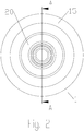
Figure 1 is a schematic cross-section cut-away side isometric view of an exemplary injection moldable dielectric cone radiator assembly.Figure 2 is a schematic front view of the injection moldable dielectric cone radiator assembly ofFigure 1 . -
Figure 3 is a schematic cut-away side view of the injection moldable dielectric cone radiator assembly ofFigure 1 , taken along line A-A ofFigure 2 . -
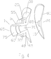
Figure 4 is a schematic cross-section cut-away side isometric view of an alternative exemplary injection moldable dielectric cone radiator assembly, with a separate sub- reflector disc. -
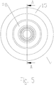
Figure 5 is a schematic front view of the injection moldable dielectric cone radiator assembly ofFigure 4 . -
Figure 6 is a schematic cut-away side view of the injection moldable dielectric cone radiator assembly ofFigure 4 , taken along line A-A ofFigure 5 . - The inventors have recognized that improvements in cone radiator sub-reflector assembly designs utilizing unitary dielectric blocks typically require manufacture of the dielectric block by machining, due to the increased size and complexity of these designs. When injection molding and/or casting methods of manufacture are attempted on the prior dielectric block type cone radiator sub-reflector assembly designs, the increased size may create issues with the setting of the dielectric polymer material, such as voids, cracks, surface sink, dimensional bends and/or sagging. Further, where the designs utilize features that inhibit mold separation, such as overhanging and/or close proximity opposing edges, the required mold, if possible at all, may become too complex to be cost effective.
- As shown in
Figures 1 -6 , a coneradiator sub-reflector assembly 1 may be configured to couple with the end of a feed boom waveguide at awaveguide transition portion 5 of a unitarydielectric block 10 which supports asub-reflector 15 at thedistal end 20. Thesub-reflector 15 and a supportingsubreflector support portion 30 are provided with an enlarged diameter for reduction of sub-reflector spill-over. - A
dielectric radiator portion 25 is situated between thewaveguide transition portion 5 and thesub-reflector support portion 30. A plurality of corrugations are provided along the outer diameter of the dielectric radiator portion as radiallyinward grooves 35. In the present embodiments, the plurality of grooves is twogrooves 35. Adistal groove 40 of thedielectric radiator portion 25 may be provided with adistal sidewall 45 that initiates thesub-reflector support portion 30. To enable smooth mold separation, thegrooves 40 may be provided with a taper that increases the groove width towards the outer diameter of thedielectric radiator portion 25. Thewaveguide transition portion 5 of thesub-reflector assembly 1 may be adapted to match a desired circular waveguide internal diameter so that thesub-reflector assembly 1 may be fitted into and retained by the waveguide end that supports thesub-reflector assembly 1 within the dish reflector of the reflector antenna proximate a focal point of the dish reflector. Thewaveguide transition portion 5 may insert into the waveguide 3 until the end of the waveguide abuts ashoulder 55 of thewaveguide transition portion 5. - The
shoulder 55 may be dimensioned to space thedielectric radiator portion 25 away from the waveguide end. - One or more step(s) 60 at the
proximal end 65 of thewaveguide transition portion 5 may be applied to a lens bore 70 of thedielectric block 10 to form an inverted
impedance transformer 75 for impedance matching purposes between the waveguide and the dielectric material of thedielectric block 10. - The
lens bore 70 extends from theproximal end 65 of thedielectric block 10 towards thedistal end 20 of thedielectric block 10 at least to thesub-reflector support portion 30. Thereby, a direct path between the waveguide 3 and thedielectric radiator portion 25 is formed, enabling tuning of the radiation pattern emitted therethrough, for example, via the depth applied to thegrooves 35 and/or diameter of thedielectric radiator portion 25. Preferably, as best shown inFigures 3 and6 , thegrooves 35 extend radially inward to a diameter less than an inner diameter of the end of the waveguide. One skilled in the art will appreciate that thedielectric radiator portion 25, in combination with the lens bore 70 therethrough, creates a dielectric lens effect in which the dimensions of thedielectric radiator portion 25 enhances a primary radiation pattern projected through thedielectric radiator portion 25 to/from thesub-reflector 15 from/to the reflector dish that thesub reflector assembly 1 is mounted within, thereby assisting the shaping of the RF radiation pattern of thesub-reflector assembly 1 and reducing the diameter ofsub-reflector 15. - As shown in
Figures 4-6 , thelens bore 70 may be provided extending entirely through thedielectric block 10, between theproximal end 65 and thedistal end 20. - As best shown in
Figure 3 ,sub-reflector 15 may be formed by applying a metallic deposition, film, sheet or other RF reflective coating to thedistal end 20 of thedielectric block 10. Alternatively, as shown inFigures 4 and6 , thesub-reflector 15 may be formed separately, for example as ametal disk 80 which seats upon the distal end of thedielectric block 10. Thedisk 80 may include akey portion 85 that keys with the lens bore 70 to position thesub-reflector 15 coaxially upon thedistal end 20 of thedielectric block 10. - Demonstrated as the largest diameter inscribed circle M possible within the confines of a cross-section of the
dielectric block 10, the centerpoint of such a circle is generally the point from which it is farthest to an edge of thedielectric block 10, the maximum material thickness. Thus, the centerpoint is the location where during injection molding of thedielectric block 10, the dielectric material will typically solidify/set last. The maximum material thickness occurs in the current embodiments located between thedistal sidewall 45 and thedistal end 20. In contrast, the maximum material thickness of prior embodiments of monolithic dielectric block cones is much larger, typically at least the entire inner diameter of the waveguide end. One skilled in the art will appreciate that the combination of the lens bore 70 and the deepenedgrooves 35 significantly reduces the maximum material thickness of thedielectric block 10, enabling the manufacture of thedielectric block 10 via injection molding with reduced voids, cracks, surface sink, dimensional bends and/or sagging defects. Alternatively, thedielectric block 10 may be manufactured by casting and/or machining which methods similarly benefit from the shallower edge angles and/or number of surface transitions required. - From the foregoing, it will be apparent that the present invention brings to the art a
sub-reflector assembly 1 for a reflector antenna with the potential for significant - manufacturing cost efficiencies. The
sub-reflector assembly 1 according to the invention are strong, lightweight and may be repeatedly cost efficiently manufactured with a very high level of precision via, for example, injection molding technology. -
- 20
- distal end
- 25
- dielectric radiator portion
- 30
- sub-reflector support portion
- 35
- groove
- 40
- distal groove
- 45
- distal sidewall
- 55
- shoulder
- 60
- step
- 65
- proximal end
- 70
- lens bore
- 75
- impedance transformer
- 80
- disk
- 85
- key portion
- Where in the foregoing description reference has been made to materials, ratios, integers or components having known equivalents then such equivalents are herein incorporated as if individually set forth.
Claims (15)
- A cone radiator sub-reflector assembly (1) for a reflector antenna with a sub-reflector (15) supported by a waveguide, comprising:a unitary dielectric block (10);a sub-reflector (15) provided at a distal end (20) of the unitary dielectric block (10);a waveguide transition portion (5) of the unitary dielectric block (10) dimensioned for insertion coupling into an end of the waveguide;a sub-reflector support portion (30) of the unitary dielectric block (10);a dielectric radiator portion (25) between the waveguide transition portion (5) and the sub-reflector support portion (30), wherein an outer diameter of the dielectric radiator portion (25) is provided with a plurality of radially inward grooves (35), characterized in that the radially inward grooves extend
radially inward to a diameter less than an inner diameter of the end of the waveguide;a lens bore (70) extending from a proximal end (65) of the unitary dielectric block (10) towards the distal end (20) of the unitary dielectric block at least to the sub-reflector support portion (30); and a maximum material thickness of the unitary dielectric block (10) occurs between a sidewall (45) of one of the radially inward grooves (35) and the sub-reflector (15). - The cone radiator sub-reflector assembly (1) of claim 1, further including an inverted impedance transformer (75) provided in the waveguide transition portion (5).
- The cone radiator sub-reflector assembly (1) of claim 1, wherein the lens bore (70) and the radially inward grooves (35) are tapered.
- The cone radiator sub-reflector assembly (1) of claim 1, wherein the sub-reflector (15) is a metal coating upon the distal end (20) of the unitary dielectric block (10).
- The cone radiator sub-reflector assembly (1) of claim 1, wherein the sub-reflector (15) is a separate metal disc seated upon the distal end (20) of the unitary dielectric block (10).
- The cone radiator sub-reflector assembly (1) of claim 1, wherein the lens bore (70) extends through the unitary dielectric block (10) to the distal end (20).
- The cone radiator sub-reflector assembly (1) of claim 1, wherein the plurality of radially inward grooves (35) is two.
- The cone radiator sub-reflector assembly (1) of claim 1, wherein an outer diameter of the dielectric radiator portion (25) is provided parallel to a longitudinal axis of the waveguide and the sub-reflector support portion (30) is provided angled outward to a periphery of the unitary dielectric block (10).
- A method for manufacturing a cone radiator sub-reflector assembly (1) for a reflector antenna with a sub-reflector (15) supported by a waveguide in accordance with claim 1, the method comprising the steps of:injection molding the unitary dielectric block (10); andcoupling the sub-reflector (15) to the distal end (20) of the unitary dielectric block.
- The method of claim 9, wherein the coupling of the sub-reflector (15) is via application of a metallic disposition upon the distal end (20) of the unitary dielectric block (10).
- The method of claim 9, wherein the coupling of the sub-reflector (15) is via positioning a separate metallic sub-reflector upon the distal end (20) of the unitary dielectric block (10).
- The method of claim 11, wherein the coupling of the separate metallic sub-reflector includes a key portion of the separate metallic sub-reflector inserted into a distal end (20) of the lens bore (70).
- The method of claim 9, wherein the coupling of the sub-reflector (15) is via application of a radio-frequency reflective coating to the distal end (20) of the unitary dielectric block (10).
- The method of claim 9, further comprising:prior to injection molding the unitary dielectric block, tuning a radiation pattern emitted through the unitary dielectric block (10) by selecting a diameter of the dielectric radiator portion (25).
- The method of claim 9, further comprising:prior to injection molding the unitary dielectric block (10), tuning a radiation pattern emitted through the dielectric block (10) by selecting a depth of the plurality of radially inward grooves (35).
Applications Claiming Priority (2)
| Application Number | Priority Date | Filing Date | Title |
|---|---|---|---|
| US13/448,995 US9105981B2 (en) | 2012-04-17 | 2012-04-17 | Dielectric lens cone radiator sub-reflector assembly |
| PCT/US2013/028190 WO2013158222A1 (en) | 2012-04-17 | 2013-02-28 | Dielectric lens cone radiator sub-reflector assembly |
Publications (3)
| Publication Number | Publication Date |
|---|---|
| EP2839539A1 EP2839539A1 (en) | 2015-02-25 |
| EP2839539A4 EP2839539A4 (en) | 2015-12-02 |
| EP2839539B1 true EP2839539B1 (en) | 2017-08-16 |
Family
ID=49324608
Family Applications (1)
| Application Number | Title | Priority Date | Filing Date |
|---|---|---|---|
| EP13778154.8A Not-in-force EP2839539B1 (en) | 2012-04-17 | 2013-02-28 | Dielectric lens cone radiator sub-reflector assembly |
Country Status (4)
| Country | Link |
|---|---|
| US (1) | US9105981B2 (en) |
| EP (1) | EP2839539B1 (en) |
| CN (1) | CN104247152B (en) |
| WO (1) | WO2013158222A1 (en) |
Families Citing this family (118)
| Publication number | Priority date | Publication date | Assignee | Title |
|---|---|---|---|---|
| US9774076B2 (en) * | 2010-08-31 | 2017-09-26 | Siklu Communication ltd. | Compact millimeter-wave radio systems and methods |
| US20140259080A1 (en) * | 2013-03-11 | 2014-09-11 | Electronic Controlled Systems, Inc. | PORTABLE SATELLITE TELEVISION SYSTEM SWITCHABLE BETWEEN Ka AND Ku FREQUENCY BANDS |
| US9525524B2 (en) | 2013-05-31 | 2016-12-20 | At&T Intellectual Property I, L.P. | Remote distributed antenna system |
| US9999038B2 (en) | 2013-05-31 | 2018-06-12 | At&T Intellectual Property I, L.P. | Remote distributed antenna system |
| US8897697B1 (en) | 2013-11-06 | 2014-11-25 | At&T Intellectual Property I, Lp | Millimeter-wave surface-wave communications |
| US9768833B2 (en) | 2014-09-15 | 2017-09-19 | At&T Intellectual Property I, L.P. | Method and apparatus for sensing a condition in a transmission medium of electromagnetic waves |
| US10063280B2 (en) | 2014-09-17 | 2018-08-28 | At&T Intellectual Property I, L.P. | Monitoring and mitigating conditions in a communication network |
| US9615269B2 (en) | 2014-10-02 | 2017-04-04 | At&T Intellectual Property I, L.P. | Method and apparatus that provides fault tolerance in a communication network |
| US9685992B2 (en) | 2014-10-03 | 2017-06-20 | At&T Intellectual Property I, L.P. | Circuit panel network and methods thereof |
| US9503189B2 (en) | 2014-10-10 | 2016-11-22 | At&T Intellectual Property I, L.P. | Method and apparatus for arranging communication sessions in a communication system |
| US9973299B2 (en) | 2014-10-14 | 2018-05-15 | At&T Intellectual Property I, L.P. | Method and apparatus for adjusting a mode of communication in a communication network |
| US9312919B1 (en) | 2014-10-21 | 2016-04-12 | At&T Intellectual Property I, Lp | Transmission device with impairment compensation and methods for use therewith |
| US9627768B2 (en) | 2014-10-21 | 2017-04-18 | At&T Intellectual Property I, L.P. | Guided-wave transmission device with non-fundamental mode propagation and methods for use therewith |
| US9780834B2 (en) | 2014-10-21 | 2017-10-03 | At&T Intellectual Property I, L.P. | Method and apparatus for transmitting electromagnetic waves |
| US9769020B2 (en) | 2014-10-21 | 2017-09-19 | At&T Intellectual Property I, L.P. | Method and apparatus for responding to events affecting communications in a communication network |
| US9653770B2 (en) | 2014-10-21 | 2017-05-16 | At&T Intellectual Property I, L.P. | Guided wave coupler, coupling module and methods for use therewith |
| US9577306B2 (en) | 2014-10-21 | 2017-02-21 | At&T Intellectual Property I, L.P. | Guided-wave transmission device and methods for use therewith |
| US9544006B2 (en) | 2014-11-20 | 2017-01-10 | At&T Intellectual Property I, L.P. | Transmission device with mode division multiplexing and methods for use therewith |
| US9997819B2 (en) | 2015-06-09 | 2018-06-12 | At&T Intellectual Property I, L.P. | Transmission medium and method for facilitating propagation of electromagnetic waves via a core |
| US9800327B2 (en) | 2014-11-20 | 2017-10-24 | At&T Intellectual Property I, L.P. | Apparatus for controlling operations of a communication device and methods thereof |
| US10340573B2 (en) | 2016-10-26 | 2019-07-02 | At&T Intellectual Property I, L.P. | Launcher with cylindrical coupling device and methods for use therewith |
| US9742462B2 (en) | 2014-12-04 | 2017-08-22 | At&T Intellectual Property I, L.P. | Transmission medium and communication interfaces and methods for use therewith |
| US10009067B2 (en) | 2014-12-04 | 2018-06-26 | At&T Intellectual Property I, L.P. | Method and apparatus for configuring a communication interface |
| US9954287B2 (en) | 2014-11-20 | 2018-04-24 | At&T Intellectual Property I, L.P. | Apparatus for converting wireless signals and electromagnetic waves and methods thereof |
| US9461706B1 (en) | 2015-07-31 | 2016-10-04 | At&T Intellectual Property I, Lp | Method and apparatus for exchanging communication signals |
| US10243784B2 (en) | 2014-11-20 | 2019-03-26 | At&T Intellectual Property I, L.P. | System for generating topology information and methods thereof |
| US9876570B2 (en) | 2015-02-20 | 2018-01-23 | At&T Intellectual Property I, Lp | Guided-wave transmission device with non-fundamental mode propagation and methods for use therewith |
| US9749013B2 (en) | 2015-03-17 | 2017-08-29 | At&T Intellectual Property I, L.P. | Method and apparatus for reducing attenuation of electromagnetic waves guided by a transmission medium |
| US9705561B2 (en) | 2015-04-24 | 2017-07-11 | At&T Intellectual Property I, L.P. | Directional coupling device and methods for use therewith |
| US10224981B2 (en) | 2015-04-24 | 2019-03-05 | At&T Intellectual Property I, Lp | Passive electrical coupling device and methods for use therewith |
| US9793954B2 (en) | 2015-04-28 | 2017-10-17 | At&T Intellectual Property I, L.P. | Magnetic coupling device and methods for use therewith |
| US9748626B2 (en) | 2015-05-14 | 2017-08-29 | At&T Intellectual Property I, L.P. | Plurality of cables having different cross-sectional shapes which are bundled together to form a transmission medium |
| US9490869B1 (en) | 2015-05-14 | 2016-11-08 | At&T Intellectual Property I, L.P. | Transmission medium having multiple cores and methods for use therewith |
| US9871282B2 (en) | 2015-05-14 | 2018-01-16 | At&T Intellectual Property I, L.P. | At least one transmission medium having a dielectric surface that is covered at least in part by a second dielectric |
| US10650940B2 (en) | 2015-05-15 | 2020-05-12 | At&T Intellectual Property I, L.P. | Transmission medium having a conductive material and methods for use therewith |
| US9917341B2 (en) | 2015-05-27 | 2018-03-13 | At&T Intellectual Property I, L.P. | Apparatus and method for launching electromagnetic waves and for modifying radial dimensions of the propagating electromagnetic waves |
| US10812174B2 (en) | 2015-06-03 | 2020-10-20 | At&T Intellectual Property I, L.P. | Client node device and methods for use therewith |
| US9866309B2 (en) | 2015-06-03 | 2018-01-09 | At&T Intellectual Property I, Lp | Host node device and methods for use therewith |
| US9912381B2 (en) | 2015-06-03 | 2018-03-06 | At&T Intellectual Property I, Lp | Network termination and methods for use therewith |
| US9913139B2 (en) | 2015-06-09 | 2018-03-06 | At&T Intellectual Property I, L.P. | Signal fingerprinting for authentication of communicating devices |
| US9820146B2 (en) | 2015-06-12 | 2017-11-14 | At&T Intellectual Property I, L.P. | Method and apparatus for authentication and identity management of communicating devices |
| US9509415B1 (en) | 2015-06-25 | 2016-11-29 | At&T Intellectual Property I, L.P. | Methods and apparatus for inducing a fundamental wave mode on a transmission medium |
| US9865911B2 (en) | 2015-06-25 | 2018-01-09 | At&T Intellectual Property I, L.P. | Waveguide system for slot radiating first electromagnetic waves that are combined into a non-fundamental wave mode second electromagnetic wave on a transmission medium |
| US9640850B2 (en) | 2015-06-25 | 2017-05-02 | At&T Intellectual Property I, L.P. | Methods and apparatus for inducing a non-fundamental wave mode on a transmission medium |
| US9847566B2 (en) | 2015-07-14 | 2017-12-19 | At&T Intellectual Property I, L.P. | Method and apparatus for adjusting a field of a signal to mitigate interference |
| US9882257B2 (en) | 2015-07-14 | 2018-01-30 | At&T Intellectual Property I, L.P. | Method and apparatus for launching a wave mode that mitigates interference |
| US10205655B2 (en) | 2015-07-14 | 2019-02-12 | At&T Intellectual Property I, L.P. | Apparatus and methods for communicating utilizing an antenna array and multiple communication paths |
| US10044409B2 (en) | 2015-07-14 | 2018-08-07 | At&T Intellectual Property I, L.P. | Transmission medium and methods for use therewith |
| US9853342B2 (en) | 2015-07-14 | 2017-12-26 | At&T Intellectual Property I, L.P. | Dielectric transmission medium connector and methods for use therewith |
| US9628116B2 (en) | 2015-07-14 | 2017-04-18 | At&T Intellectual Property I, L.P. | Apparatus and methods for transmitting wireless signals |
| US10148016B2 (en) | 2015-07-14 | 2018-12-04 | At&T Intellectual Property I, L.P. | Apparatus and methods for communicating utilizing an antenna array |
| US10090606B2 (en) | 2015-07-15 | 2018-10-02 | At&T Intellectual Property I, L.P. | Antenna system with dielectric array and methods for use therewith |
| US9871283B2 (en) | 2015-07-23 | 2018-01-16 | At&T Intellectual Property I, Lp | Transmission medium having a dielectric core comprised of plural members connected by a ball and socket configuration |
| US9912027B2 (en) | 2015-07-23 | 2018-03-06 | At&T Intellectual Property I, L.P. | Method and apparatus for exchanging communication signals |
| US9749053B2 (en) | 2015-07-23 | 2017-08-29 | At&T Intellectual Property I, L.P. | Node device, repeater and methods for use therewith |
| US9948333B2 (en) | 2015-07-23 | 2018-04-17 | At&T Intellectual Property I, L.P. | Method and apparatus for wireless communications to mitigate interference |
| US9735833B2 (en) | 2015-07-31 | 2017-08-15 | At&T Intellectual Property I, L.P. | Method and apparatus for communications management in a neighborhood network |
| US9967173B2 (en) | 2015-07-31 | 2018-05-08 | At&T Intellectual Property I, L.P. | Method and apparatus for authentication and identity management of communicating devices |
| US9904535B2 (en) | 2015-09-14 | 2018-02-27 | At&T Intellectual Property I, L.P. | Method and apparatus for distributing software |
| US9769128B2 (en) | 2015-09-28 | 2017-09-19 | At&T Intellectual Property I, L.P. | Method and apparatus for encryption of communications over a network |
| US9729197B2 (en) | 2015-10-01 | 2017-08-08 | At&T Intellectual Property I, L.P. | Method and apparatus for communicating network management traffic over a network |
| US9876264B2 (en) | 2015-10-02 | 2018-01-23 | At&T Intellectual Property I, Lp | Communication system, guided wave switch and methods for use therewith |
| US10355367B2 (en) | 2015-10-16 | 2019-07-16 | At&T Intellectual Property I, L.P. | Antenna structure for exchanging wireless signals |
| US9860075B1 (en) | 2016-08-26 | 2018-01-02 | At&T Intellectual Property I, L.P. | Method and communication node for broadband distribution |
| US11489259B2 (en) * | 2016-09-23 | 2022-11-01 | Commscope Technologies Llc | Dual-band parabolic reflector microwave antenna systems |
| US10374316B2 (en) | 2016-10-21 | 2019-08-06 | At&T Intellectual Property I, L.P. | System and dielectric antenna with non-uniform dielectric |
| US10811767B2 (en) | 2016-10-21 | 2020-10-20 | At&T Intellectual Property I, L.P. | System and dielectric antenna with convex dielectric radome |
| US10312567B2 (en) | 2016-10-26 | 2019-06-04 | At&T Intellectual Property I, L.P. | Launcher with planar strip antenna and methods for use therewith |
| US10498044B2 (en) | 2016-11-03 | 2019-12-03 | At&T Intellectual Property I, L.P. | Apparatus for configuring a surface of an antenna |
| US10225025B2 (en) | 2016-11-03 | 2019-03-05 | At&T Intellectual Property I, L.P. | Method and apparatus for detecting a fault in a communication system |
| US10224634B2 (en) | 2016-11-03 | 2019-03-05 | At&T Intellectual Property I, L.P. | Methods and apparatus for adjusting an operational characteristic of an antenna |
| US10291334B2 (en) | 2016-11-03 | 2019-05-14 | At&T Intellectual Property I, L.P. | System for detecting a fault in a communication system |
| US10090594B2 (en) | 2016-11-23 | 2018-10-02 | At&T Intellectual Property I, L.P. | Antenna system having structural configurations for assembly |
| US10178445B2 (en) | 2016-11-23 | 2019-01-08 | At&T Intellectual Property I, L.P. | Methods, devices, and systems for load balancing between a plurality of waveguides |
| US10535928B2 (en) | 2016-11-23 | 2020-01-14 | At&T Intellectual Property I, L.P. | Antenna system and methods for use therewith |
| US10340603B2 (en) | 2016-11-23 | 2019-07-02 | At&T Intellectual Property I, L.P. | Antenna system having shielded structural configurations for assembly |
| US10340601B2 (en) | 2016-11-23 | 2019-07-02 | At&T Intellectual Property I, L.P. | Multi-antenna system and methods for use therewith |
| US10305190B2 (en) | 2016-12-01 | 2019-05-28 | At&T Intellectual Property I, L.P. | Reflecting dielectric antenna system and methods for use therewith |
| US10361489B2 (en) | 2016-12-01 | 2019-07-23 | At&T Intellectual Property I, L.P. | Dielectric dish antenna system and methods for use therewith |
| US10727599B2 (en) | 2016-12-06 | 2020-07-28 | At&T Intellectual Property I, L.P. | Launcher with slot antenna and methods for use therewith |
| US10819035B2 (en) | 2016-12-06 | 2020-10-27 | At&T Intellectual Property I, L.P. | Launcher with helical antenna and methods for use therewith |
| US10637149B2 (en) | 2016-12-06 | 2020-04-28 | At&T Intellectual Property I, L.P. | Injection molded dielectric antenna and methods for use therewith |
| US10020844B2 (en) | 2016-12-06 | 2018-07-10 | T&T Intellectual Property I, L.P. | Method and apparatus for broadcast communication via guided waves |
| US10439675B2 (en) | 2016-12-06 | 2019-10-08 | At&T Intellectual Property I, L.P. | Method and apparatus for repeating guided wave communication signals |
| US10382976B2 (en) | 2016-12-06 | 2019-08-13 | At&T Intellectual Property I, L.P. | Method and apparatus for managing wireless communications based on communication paths and network device positions |
| US10135145B2 (en) | 2016-12-06 | 2018-11-20 | At&T Intellectual Property I, L.P. | Apparatus and methods for generating an electromagnetic wave along a transmission medium |
| US10694379B2 (en) | 2016-12-06 | 2020-06-23 | At&T Intellectual Property I, L.P. | Waveguide system with device-based authentication and methods for use therewith |
| US10326494B2 (en) | 2016-12-06 | 2019-06-18 | At&T Intellectual Property I, L.P. | Apparatus for measurement de-embedding and methods for use therewith |
| US9927517B1 (en) | 2016-12-06 | 2018-03-27 | At&T Intellectual Property I, L.P. | Apparatus and methods for sensing rainfall |
| US10755542B2 (en) | 2016-12-06 | 2020-08-25 | At&T Intellectual Property I, L.P. | Method and apparatus for surveillance via guided wave communication |
| US10446936B2 (en) | 2016-12-07 | 2019-10-15 | At&T Intellectual Property I, L.P. | Multi-feed dielectric antenna system and methods for use therewith |
| US10389029B2 (en) | 2016-12-07 | 2019-08-20 | At&T Intellectual Property I, L.P. | Multi-feed dielectric antenna system with core selection and methods for use therewith |
| US10547348B2 (en) | 2016-12-07 | 2020-01-28 | At&T Intellectual Property I, L.P. | Method and apparatus for switching transmission mediums in a communication system |
| US10359749B2 (en) | 2016-12-07 | 2019-07-23 | At&T Intellectual Property I, L.P. | Method and apparatus for utilities management via guided wave communication |
| US9893795B1 (en) | 2016-12-07 | 2018-02-13 | At&T Intellectual Property I, Lp | Method and repeater for broadband distribution |
| US10168695B2 (en) | 2016-12-07 | 2019-01-01 | At&T Intellectual Property I, L.P. | Method and apparatus for controlling an unmanned aircraft |
| US10027397B2 (en) | 2016-12-07 | 2018-07-17 | At&T Intellectual Property I, L.P. | Distributed antenna system and methods for use therewith |
| US10243270B2 (en) | 2016-12-07 | 2019-03-26 | At&T Intellectual Property I, L.P. | Beam adaptive multi-feed dielectric antenna system and methods for use therewith |
| US10139820B2 (en) | 2016-12-07 | 2018-11-27 | At&T Intellectual Property I, L.P. | Method and apparatus for deploying equipment of a communication system |
| US10777873B2 (en) | 2016-12-08 | 2020-09-15 | At&T Intellectual Property I, L.P. | Method and apparatus for mounting network devices |
| US10389037B2 (en) | 2016-12-08 | 2019-08-20 | At&T Intellectual Property I, L.P. | Apparatus and methods for selecting sections of an antenna array and use therewith |
| US10411356B2 (en) | 2016-12-08 | 2019-09-10 | At&T Intellectual Property I, L.P. | Apparatus and methods for selectively targeting communication devices with an antenna array |
| US10938108B2 (en) | 2016-12-08 | 2021-03-02 | At&T Intellectual Property I, L.P. | Frequency selective multi-feed dielectric antenna system and methods for use therewith |
| US9911020B1 (en) | 2016-12-08 | 2018-03-06 | At&T Intellectual Property I, L.P. | Method and apparatus for tracking via a radio frequency identification device |
| US10916969B2 (en) | 2016-12-08 | 2021-02-09 | At&T Intellectual Property I, L.P. | Method and apparatus for providing power using an inductive coupling |
| US10601494B2 (en) | 2016-12-08 | 2020-03-24 | At&T Intellectual Property I, L.P. | Dual-band communication device and method for use therewith |
| US10530505B2 (en) | 2016-12-08 | 2020-01-07 | At&T Intellectual Property I, L.P. | Apparatus and methods for launching electromagnetic waves along a transmission medium |
| US10103422B2 (en) | 2016-12-08 | 2018-10-16 | At&T Intellectual Property I, L.P. | Method and apparatus for mounting network devices |
| US10069535B2 (en) | 2016-12-08 | 2018-09-04 | At&T Intellectual Property I, L.P. | Apparatus and methods for launching electromagnetic waves having a certain electric field structure |
| US9998870B1 (en) | 2016-12-08 | 2018-06-12 | At&T Intellectual Property I, L.P. | Method and apparatus for proximity sensing |
| US10326689B2 (en) | 2016-12-08 | 2019-06-18 | At&T Intellectual Property I, L.P. | Method and system for providing alternative communication paths |
| US9838896B1 (en) | 2016-12-09 | 2017-12-05 | At&T Intellectual Property I, L.P. | Method and apparatus for assessing network coverage |
| US10264586B2 (en) | 2016-12-09 | 2019-04-16 | At&T Mobility Ii Llc | Cloud-based packet controller and methods for use therewith |
| US10340983B2 (en) | 2016-12-09 | 2019-07-02 | At&T Intellectual Property I, L.P. | Method and apparatus for surveying remote sites via guided wave communications |
| US9973940B1 (en) | 2017-02-27 | 2018-05-15 | At&T Intellectual Property I, L.P. | Apparatus and methods for dynamic impedance matching of a guided wave launcher |
| US10298293B2 (en) | 2017-03-13 | 2019-05-21 | At&T Intellectual Property I, L.P. | Apparatus of communication utilizing wireless network devices |
| RU173936U1 (en) * | 2017-03-27 | 2017-09-20 | Акционерное общество "Научно-исследовательский институт Приборостроения имени В.В. Тихомирова" | THE ELECTRONIC UNIT |
| EP3622582B1 (en) * | 2017-06-30 | 2021-10-20 | Huawei Technologies Co., Ltd. | Antenna feeder assembly of multi-band antenna and multi-band antenna |
Family Cites Families (23)
| Publication number | Priority date | Publication date | Assignee | Title |
|---|---|---|---|---|
| US2605416A (en) | 1945-09-19 | 1952-07-29 | Foster John Stuart | Directive system for wave guide feed to parabolic reflector |
| DE3579308D1 (en) | 1984-07-02 | 1990-09-27 | Marconi Co Ltd | CASSEGRAIN ANTENNA SYSTEM. |
| US4673945A (en) | 1984-09-24 | 1987-06-16 | Alpha Industries, Inc. | Backfire antenna feeding |
| NO862192D0 (en) | 1986-06-03 | 1986-06-03 | Sintef | REFLECTOR ANTENNA WITH SELF-SUSTAINABLE MEASUREMENT ELEMENT. |
| DE4002913A1 (en) * | 1990-02-01 | 1991-08-08 | Ant Nachrichtentech | DOUBLE REFLECTOR ANTENNA |
| US5959590A (en) | 1996-08-08 | 1999-09-28 | Endgate Corporation | Low sidelobe reflector antenna system employing a corrugated subreflector |
| US6020859A (en) * | 1996-09-26 | 2000-02-01 | Kildal; Per-Simon | Reflector antenna with a self-supported feed |
| US6137449A (en) | 1996-09-26 | 2000-10-24 | Kildal; Per-Simon | Reflector antenna with a self-supported feed |
| DE69834968T2 (en) | 1997-02-14 | 2006-11-16 | Andrew Ag, Bachenbulach | Dual reflector microwave antenna |
| US5973652A (en) | 1997-05-22 | 1999-10-26 | Endgate Corporation | Reflector antenna with improved return loss |
| DE19952819A1 (en) | 1999-11-02 | 2001-07-12 | Rr Elektronische Geraete Gmbh | Reflector antenna and method of manufacturing a sub-reflector |
| SE515493C2 (en) | 1999-12-28 | 2001-08-13 | Ericsson Telefon Ab L M | Sub reflector, feeder and reflector antenna including such a sub reflector. |
| US6522305B2 (en) | 2000-02-25 | 2003-02-18 | Andrew Corporation | Microwave antennas |
| DE60027743T2 (en) | 2000-12-27 | 2006-11-09 | Marconi Communications Gmbh | Antenna with Cassegrain feeder |
| US6697027B2 (en) | 2001-08-23 | 2004-02-24 | John P. Mahon | High gain, low side lobe dual reflector microwave antenna |
| US6862000B2 (en) | 2002-01-28 | 2005-03-01 | The Boeing Company | Reflector antenna having low-dielectric support tube for sub-reflectors and feeds |
| US6724349B1 (en) | 2002-11-12 | 2004-04-20 | L-3 Communications Corporation | Splashplate antenna system with improved waveguide and splashplate (sub-reflector) designs |
| FR2856525B1 (en) | 2003-06-17 | 2005-09-02 | Cit Alcatel | POWER SUPPLY FOR A REFLECTOR ANTENNA. |
| US6985120B2 (en) | 2003-07-25 | 2006-01-10 | Andrew Corporation | Reflector antenna with injection molded feed assembly |
| US6919855B2 (en) * | 2003-09-18 | 2005-07-19 | Andrew Corporation | Tuned perturbation cone feed for reflector antenna |
| US7907097B2 (en) | 2007-07-17 | 2011-03-15 | Andrew Llc | Self-supporting unitary feed assembly |
| CN102782939A (en) | 2009-12-16 | 2012-11-14 | 安德鲁有限责任公司 | Method and apparatus for reflector antenna with vertex region scatter compensation |
| US20110309987A1 (en) | 2010-06-20 | 2011-12-22 | Siklu Communication ltd. | Reflector antenna including radome |
-
2012
- 2012-04-17 US US13/448,995 patent/US9105981B2/en active Active
-
2013
- 2013-02-28 WO PCT/US2013/028190 patent/WO2013158222A1/en not_active Ceased
- 2013-02-28 EP EP13778154.8A patent/EP2839539B1/en not_active Not-in-force
- 2013-02-28 CN CN201380017759.4A patent/CN104247152B/en not_active Expired - Fee Related
Non-Patent Citations (1)
| Title |
|---|
| None * |
Also Published As
| Publication number | Publication date |
|---|---|
| CN104247152B (en) | 2016-06-08 |
| CN104247152A (en) | 2014-12-24 |
| US9105981B2 (en) | 2015-08-11 |
| EP2839539A1 (en) | 2015-02-25 |
| US20130271348A1 (en) | 2013-10-17 |
| EP2839539A4 (en) | 2015-12-02 |
| WO2013158222A1 (en) | 2013-10-24 |
Similar Documents
| Publication | Publication Date | Title |
|---|---|---|
| US9105981B2 (en) | Dielectric lens cone radiator sub-reflector assembly | |
| EP2839538B1 (en) | Injection moldable cone radiator sub-reflector assembly | |
| EP2686906B1 (en) | Low sidelobe reflector antenna | |
| US9019164B2 (en) | Low sidelobe reflector antenna with shield | |
| US9948009B2 (en) | Controlled illumination dielectric cone radiator for reflector antenna | |
| EP2850695A1 (en) | Low sidelobe reflector antenna with shield | |
| US4929962A (en) | Feed horn for a telecommunications antenna | |
| US10170844B2 (en) | Method for dish reflector illumination via sub-reflector assembly with dielectric radiator portion | |
| EP3516737B1 (en) | Dual-band parabolic reflector microwave antenna systems | |
| WO2019060072A1 (en) | Parabolic reflector antennas having feeds with enhanced radiation pattern control | |
| US20150042527A1 (en) | Sub-Reflector Assembly With Extended Dielectric Radiator | |
| US20210376480A1 (en) | Parabolic reflector antennas with improved cylindrically-shaped shields | |
| US11075466B2 (en) | Parabolic reflector antennas that support low side lobe radiation patterns | |
| US11888230B1 (en) | Antenna assembly including feed system having a sub-reflector |
Legal Events
| Date | Code | Title | Description |
|---|---|---|---|
| PUAI | Public reference made under article 153(3) epc to a published international application that has entered the european phase |
Free format text: ORIGINAL CODE: 0009012 |
|
| 17P | Request for examination filed |
Effective date: 20140923 |
|
| AK | Designated contracting states |
Kind code of ref document: A1 Designated state(s): AL AT BE BG CH CY CZ DE DK EE ES FI FR GB GR HR HU IE IS IT LI LT LU LV MC MK MT NL NO PL PT RO RS SE SI SK SM TR |
|
| AX | Request for extension of the european patent |
Extension state: BA ME |
|
| RIN1 | Information on inventor provided before grant (corrected) |
Inventor name: WRIGHT, ALASTAIR Inventor name: LAWSON, BRIAN Inventor name: BRANDAU, RONALD Inventor name: SYED, JUNAID UL ISLAM Inventor name: TASKER, ALAN |
|
| RAP1 | Party data changed (applicant data changed or rights of an application transferred) |
Owner name: COMMSCOPE TECHNOLOGIES LLC |
|
| DAX | Request for extension of the european patent (deleted) | ||
| RA4 | Supplementary search report drawn up and despatched (corrected) |
Effective date: 20151030 |
|
| RIC1 | Information provided on ipc code assigned before grant |
Ipc: H01Q 19/08 20060101AFI20151026BHEP Ipc: B29C 45/00 20060101ALI20151026BHEP Ipc: H01Q 13/24 20060101ALI20151026BHEP Ipc: H01Q 19/13 20060101ALI20151026BHEP Ipc: H01Q 19/19 20060101ALI20151026BHEP |
|
| REG | Reference to a national code |
Ref country code: DE Ref legal event code: R079 Ref document number: 602013025166 Country of ref document: DE Free format text: PREVIOUS MAIN CLASS: H01Q0015140000 Ipc: H01Q0019080000 |
|
| GRAP | Despatch of communication of intention to grant a patent |
Free format text: ORIGINAL CODE: EPIDOSNIGR1 |
|
| INTG | Intention to grant announced |
Effective date: 20170324 |
|
| RIC1 | Information provided on ipc code assigned before grant |
Ipc: H01Q 19/19 20060101ALI20170310BHEP Ipc: H01Q 19/08 20060101AFI20170310BHEP Ipc: H01Q 13/24 20060101ALI20170310BHEP Ipc: H01Q 19/13 20060101ALI20170310BHEP Ipc: B29C 45/00 20060101ALI20170310BHEP |
|
| GRAS | Grant fee paid |
Free format text: ORIGINAL CODE: EPIDOSNIGR3 |
|
| GRAA | (expected) grant |
Free format text: ORIGINAL CODE: 0009210 |
|
| AK | Designated contracting states |
Kind code of ref document: B1 Designated state(s): AL AT BE BG CH CY CZ DE DK EE ES FI FR GB GR HR HU IE IS IT LI LT LU LV MC MK MT NL NO PL PT RO RS SE SI SK SM TR |
|
| REG | Reference to a national code |
Ref country code: GB Ref legal event code: FG4D |
|
| REG | Reference to a national code |
Ref country code: CH Ref legal event code: EP |
|
| REG | Reference to a national code |
Ref country code: IE Ref legal event code: FG4D |
|
| REG | Reference to a national code |
Ref country code: AT Ref legal event code: REF Ref document number: 919919 Country of ref document: AT Kind code of ref document: T Effective date: 20170915 |
|
| REG | Reference to a national code |
Ref country code: DE Ref legal event code: R096 Ref document number: 602013025166 Country of ref document: DE |
|
| REG | Reference to a national code |
Ref country code: SE Ref legal event code: TRGR |
|
| REG | Reference to a national code |
Ref country code: NL Ref legal event code: MP Effective date: 20170816 |
|
| REG | Reference to a national code |
Ref country code: LT Ref legal event code: MG4D |
|
| REG | Reference to a national code |
Ref country code: AT Ref legal event code: MK05 Ref document number: 919919 Country of ref document: AT Kind code of ref document: T Effective date: 20170816 |
|
| PG25 | Lapsed in a contracting state [announced via postgrant information from national office to epo] |
Ref country code: FI Free format text: LAPSE BECAUSE OF FAILURE TO SUBMIT A TRANSLATION OF THE DESCRIPTION OR TO PAY THE FEE WITHIN THE PRESCRIBED TIME-LIMIT Effective date: 20170816 Ref country code: LT Free format text: LAPSE BECAUSE OF FAILURE TO SUBMIT A TRANSLATION OF THE DESCRIPTION OR TO PAY THE FEE WITHIN THE PRESCRIBED TIME-LIMIT Effective date: 20170816 Ref country code: AT Free format text: LAPSE BECAUSE OF FAILURE TO SUBMIT A TRANSLATION OF THE DESCRIPTION OR TO PAY THE FEE WITHIN THE PRESCRIBED TIME-LIMIT Effective date: 20170816 Ref country code: NL Free format text: LAPSE BECAUSE OF FAILURE TO SUBMIT A TRANSLATION OF THE DESCRIPTION OR TO PAY THE FEE WITHIN THE PRESCRIBED TIME-LIMIT Effective date: 20170816 Ref country code: NO Free format text: LAPSE BECAUSE OF FAILURE TO SUBMIT A TRANSLATION OF THE DESCRIPTION OR TO PAY THE FEE WITHIN THE PRESCRIBED TIME-LIMIT Effective date: 20171116 |
|
| REG | Reference to a national code |
Ref country code: FR Ref legal event code: PLFP Year of fee payment: 6 |
|
| PG25 | Lapsed in a contracting state [announced via postgrant information from national office to epo] |
Ref country code: RS Free format text: LAPSE BECAUSE OF FAILURE TO SUBMIT A TRANSLATION OF THE DESCRIPTION OR TO PAY THE FEE WITHIN THE PRESCRIBED TIME-LIMIT Effective date: 20170816 Ref country code: ES Free format text: LAPSE BECAUSE OF FAILURE TO SUBMIT A TRANSLATION OF THE DESCRIPTION OR TO PAY THE FEE WITHIN THE PRESCRIBED TIME-LIMIT Effective date: 20170816 Ref country code: LV Free format text: LAPSE BECAUSE OF FAILURE TO SUBMIT A TRANSLATION OF THE DESCRIPTION OR TO PAY THE FEE WITHIN THE PRESCRIBED TIME-LIMIT Effective date: 20170816 Ref country code: GR Free format text: LAPSE BECAUSE OF FAILURE TO SUBMIT A TRANSLATION OF THE DESCRIPTION OR TO PAY THE FEE WITHIN THE PRESCRIBED TIME-LIMIT Effective date: 20171117 Ref country code: PL Free format text: LAPSE BECAUSE OF FAILURE TO SUBMIT A TRANSLATION OF THE DESCRIPTION OR TO PAY THE FEE WITHIN THE PRESCRIBED TIME-LIMIT Effective date: 20170816 Ref country code: BG Free format text: LAPSE BECAUSE OF FAILURE TO SUBMIT A TRANSLATION OF THE DESCRIPTION OR TO PAY THE FEE WITHIN THE PRESCRIBED TIME-LIMIT Effective date: 20171116 Ref country code: IS Free format text: LAPSE BECAUSE OF FAILURE TO SUBMIT A TRANSLATION OF THE DESCRIPTION OR TO PAY THE FEE WITHIN THE PRESCRIBED TIME-LIMIT Effective date: 20171216 |
|
| PG25 | Lapsed in a contracting state [announced via postgrant information from national office to epo] |
Ref country code: CZ Free format text: LAPSE BECAUSE OF FAILURE TO SUBMIT A TRANSLATION OF THE DESCRIPTION OR TO PAY THE FEE WITHIN THE PRESCRIBED TIME-LIMIT Effective date: 20170816 Ref country code: DK Free format text: LAPSE BECAUSE OF FAILURE TO SUBMIT A TRANSLATION OF THE DESCRIPTION OR TO PAY THE FEE WITHIN THE PRESCRIBED TIME-LIMIT Effective date: 20170816 Ref country code: RO Free format text: LAPSE BECAUSE OF FAILURE TO SUBMIT A TRANSLATION OF THE DESCRIPTION OR TO PAY THE FEE WITHIN THE PRESCRIBED TIME-LIMIT Effective date: 20170816 |
|
| REG | Reference to a national code |
Ref country code: DE Ref legal event code: R097 Ref document number: 602013025166 Country of ref document: DE |
|
| PG25 | Lapsed in a contracting state [announced via postgrant information from national office to epo] |
Ref country code: SK Free format text: LAPSE BECAUSE OF FAILURE TO SUBMIT A TRANSLATION OF THE DESCRIPTION OR TO PAY THE FEE WITHIN THE PRESCRIBED TIME-LIMIT Effective date: 20170816 Ref country code: EE Free format text: LAPSE BECAUSE OF FAILURE TO SUBMIT A TRANSLATION OF THE DESCRIPTION OR TO PAY THE FEE WITHIN THE PRESCRIBED TIME-LIMIT Effective date: 20170816 Ref country code: SM Free format text: LAPSE BECAUSE OF FAILURE TO SUBMIT A TRANSLATION OF THE DESCRIPTION OR TO PAY THE FEE WITHIN THE PRESCRIBED TIME-LIMIT Effective date: 20170816 Ref country code: IT Free format text: LAPSE BECAUSE OF FAILURE TO SUBMIT A TRANSLATION OF THE DESCRIPTION OR TO PAY THE FEE WITHIN THE PRESCRIBED TIME-LIMIT Effective date: 20170816 |
|
| PLBE | No opposition filed within time limit |
Free format text: ORIGINAL CODE: 0009261 |
|
| STAA | Information on the status of an ep patent application or granted ep patent |
Free format text: STATUS: NO OPPOSITION FILED WITHIN TIME LIMIT |
|
| 26N | No opposition filed |
Effective date: 20180517 |
|
| PG25 | Lapsed in a contracting state [announced via postgrant information from national office to epo] |
Ref country code: SI Free format text: LAPSE BECAUSE OF FAILURE TO SUBMIT A TRANSLATION OF THE DESCRIPTION OR TO PAY THE FEE WITHIN THE PRESCRIBED TIME-LIMIT Effective date: 20170816 |
|
| REG | Reference to a national code |
Ref country code: DE Ref legal event code: R119 Ref document number: 602013025166 Country of ref document: DE |
|
| REG | Reference to a national code |
Ref country code: CH Ref legal event code: PL |
|
| PG25 | Lapsed in a contracting state [announced via postgrant information from national office to epo] |
Ref country code: MC Free format text: LAPSE BECAUSE OF FAILURE TO SUBMIT A TRANSLATION OF THE DESCRIPTION OR TO PAY THE FEE WITHIN THE PRESCRIBED TIME-LIMIT Effective date: 20170816 |
|
| GBPC | Gb: european patent ceased through non-payment of renewal fee |
Effective date: 20180228 |
|
| REG | Reference to a national code |
Ref country code: IE Ref legal event code: MM4A |
|
| REG | Reference to a national code |
Ref country code: BE Ref legal event code: MM Effective date: 20180228 |
|
| PG25 | Lapsed in a contracting state [announced via postgrant information from national office to epo] |
Ref country code: LU Free format text: LAPSE BECAUSE OF NON-PAYMENT OF DUE FEES Effective date: 20180228 Ref country code: LI Free format text: LAPSE BECAUSE OF NON-PAYMENT OF DUE FEES Effective date: 20180228 Ref country code: CH Free format text: LAPSE BECAUSE OF NON-PAYMENT OF DUE FEES Effective date: 20180228 |
|
| PG25 | Lapsed in a contracting state [announced via postgrant information from national office to epo] |
Ref country code: DE Free format text: LAPSE BECAUSE OF NON-PAYMENT OF DUE FEES Effective date: 20180901 Ref country code: IE Free format text: LAPSE BECAUSE OF NON-PAYMENT OF DUE FEES Effective date: 20180228 |
|
| PG25 | Lapsed in a contracting state [announced via postgrant information from national office to epo] |
Ref country code: GB Free format text: LAPSE BECAUSE OF NON-PAYMENT OF DUE FEES Effective date: 20180228 Ref country code: BE Free format text: LAPSE BECAUSE OF NON-PAYMENT OF DUE FEES Effective date: 20180228 |
|
| PG25 | Lapsed in a contracting state [announced via postgrant information from national office to epo] |
Ref country code: MT Free format text: LAPSE BECAUSE OF NON-PAYMENT OF DUE FEES Effective date: 20180228 |
|
| PG25 | Lapsed in a contracting state [announced via postgrant information from national office to epo] |
Ref country code: TR Free format text: LAPSE BECAUSE OF FAILURE TO SUBMIT A TRANSLATION OF THE DESCRIPTION OR TO PAY THE FEE WITHIN THE PRESCRIBED TIME-LIMIT Effective date: 20170816 |
|
| PG25 | Lapsed in a contracting state [announced via postgrant information from national office to epo] |
Ref country code: PT Free format text: LAPSE BECAUSE OF FAILURE TO SUBMIT A TRANSLATION OF THE DESCRIPTION OR TO PAY THE FEE WITHIN THE PRESCRIBED TIME-LIMIT Effective date: 20170816 |
|
| PG25 | Lapsed in a contracting state [announced via postgrant information from national office to epo] |
Ref country code: CY Free format text: LAPSE BECAUSE OF FAILURE TO SUBMIT A TRANSLATION OF THE DESCRIPTION OR TO PAY THE FEE WITHIN THE PRESCRIBED TIME-LIMIT Effective date: 20170816 Ref country code: HR Free format text: LAPSE BECAUSE OF FAILURE TO SUBMIT A TRANSLATION OF THE DESCRIPTION OR TO PAY THE FEE WITHIN THE PRESCRIBED TIME-LIMIT Effective date: 20170816 Ref country code: HU Free format text: LAPSE BECAUSE OF FAILURE TO SUBMIT A TRANSLATION OF THE DESCRIPTION OR TO PAY THE FEE WITHIN THE PRESCRIBED TIME-LIMIT; INVALID AB INITIO Effective date: 20130228 Ref country code: MK Free format text: LAPSE BECAUSE OF NON-PAYMENT OF DUE FEES Effective date: 20170816 |
|
| PG25 | Lapsed in a contracting state [announced via postgrant information from national office to epo] |
Ref country code: AL Free format text: LAPSE BECAUSE OF FAILURE TO SUBMIT A TRANSLATION OF THE DESCRIPTION OR TO PAY THE FEE WITHIN THE PRESCRIBED TIME-LIMIT Effective date: 20170816 |
|
| PGFP | Annual fee paid to national office [announced via postgrant information from national office to epo] |
Ref country code: FR Payment date: 20230223 Year of fee payment: 11 |
|
| PGFP | Annual fee paid to national office [announced via postgrant information from national office to epo] |
Ref country code: SE Payment date: 20230227 Year of fee payment: 11 |
|
| P01 | Opt-out of the competence of the unified patent court (upc) registered |
Effective date: 20230530 |
|
| REG | Reference to a national code |
Ref country code: SE Ref legal event code: EUG |
|
| PG25 | Lapsed in a contracting state [announced via postgrant information from national office to epo] |
Ref country code: FR Free format text: LAPSE BECAUSE OF NON-PAYMENT OF DUE FEES Effective date: 20240229 |
|
| PG25 | Lapsed in a contracting state [announced via postgrant information from national office to epo] |
Ref country code: FR Free format text: LAPSE BECAUSE OF NON-PAYMENT OF DUE FEES Effective date: 20240229 |
|
| PG25 | Lapsed in a contracting state [announced via postgrant information from national office to epo] |
Ref country code: SE Free format text: LAPSE BECAUSE OF NON-PAYMENT OF DUE FEES Effective date: 20240229 |