EP2838194A1 - Amplifier circuits - Google Patents
Amplifier circuits Download PDFInfo
- Publication number
- EP2838194A1 EP2838194A1 EP20130290190 EP13290190A EP2838194A1 EP 2838194 A1 EP2838194 A1 EP 2838194A1 EP 20130290190 EP20130290190 EP 20130290190 EP 13290190 A EP13290190 A EP 13290190A EP 2838194 A1 EP2838194 A1 EP 2838194A1
- Authority
- EP
- European Patent Office
- Prior art keywords
- circuit
- source
- substrate
- amplifier
- amplifier circuits
- Prior art date
- Legal status (The legal status is an assumption and is not a legal conclusion. Google has not performed a legal analysis and makes no representation as to the accuracy of the status listed.)
- Granted
Links
Images



Classifications
-
- H—ELECTRICITY
- H03—ELECTRONIC CIRCUITRY
- H03F—AMPLIFIERS
- H03F3/00—Amplifiers with only discharge tubes or only semiconductor devices as amplifying elements
- H03F3/45—Differential amplifiers
- H03F3/45071—Differential amplifiers with semiconductor devices only
- H03F3/45076—Differential amplifiers with semiconductor devices only characterised by the way of implementation of the active amplifying circuit in the differential amplifier
- H03F3/45179—Differential amplifiers with semiconductor devices only characterised by the way of implementation of the active amplifying circuit in the differential amplifier using MOSFET transistors as the active amplifying circuit
-
- H—ELECTRICITY
- H03—ELECTRONIC CIRCUITRY
- H03F—AMPLIFIERS
- H03F3/00—Amplifiers with only discharge tubes or only semiconductor devices as amplifying elements
- H03F3/189—High-frequency amplifiers, e.g. radio frequency amplifiers
- H03F3/19—High-frequency amplifiers, e.g. radio frequency amplifiers with semiconductor devices only
- H03F3/193—High-frequency amplifiers, e.g. radio frequency amplifiers with semiconductor devices only with field-effect devices
-
- H—ELECTRICITY
- H03—ELECTRONIC CIRCUITRY
- H03F—AMPLIFIERS
- H03F3/00—Amplifiers with only discharge tubes or only semiconductor devices as amplifying elements
- H03F3/20—Power amplifiers, e.g. Class B amplifiers, Class C amplifiers
- H03F3/21—Power amplifiers, e.g. Class B amplifiers, Class C amplifiers with semiconductor devices only
-
- H—ELECTRICITY
- H03—ELECTRONIC CIRCUITRY
- H03F—AMPLIFIERS
- H03F3/00—Amplifiers with only discharge tubes or only semiconductor devices as amplifying elements
- H03F3/26—Push-pull amplifiers; Phase-splitters therefor
- H03F3/265—Push-pull amplifiers; Phase-splitters therefor with field-effect transistors only
-
- H—ELECTRICITY
- H03—ELECTRONIC CIRCUITRY
- H03F—AMPLIFIERS
- H03F3/00—Amplifiers with only discharge tubes or only semiconductor devices as amplifying elements
- H03F3/45—Differential amplifiers
-
- H—ELECTRICITY
- H03—ELECTRONIC CIRCUITRY
- H03F—AMPLIFIERS
- H03F3/00—Amplifiers with only discharge tubes or only semiconductor devices as amplifying elements
- H03F3/45—Differential amplifiers
- H03F3/45071—Differential amplifiers with semiconductor devices only
- H03F3/45076—Differential amplifiers with semiconductor devices only characterised by the way of implementation of the active amplifying circuit in the differential amplifier
- H03F3/45179—Differential amplifiers with semiconductor devices only characterised by the way of implementation of the active amplifying circuit in the differential amplifier using MOSFET transistors as the active amplifying circuit
- H03F3/45183—Long tailed pairs
-
- H—ELECTRICITY
- H10—SEMICONDUCTOR DEVICES; ELECTRIC SOLID-STATE DEVICES NOT OTHERWISE PROVIDED FOR
- H10D—INORGANIC ELECTRIC SEMICONDUCTOR DEVICES
- H10D84/00—Integrated devices formed in or on semiconductor substrates that comprise only semiconducting layers, e.g. on Si wafers or on GaAs-on-Si wafers
- H10D84/101—Integrated devices comprising main components and built-in components, e.g. IGBT having built-in freewheel diode
- H10D84/151—LDMOS having built-in components
-
- H—ELECTRICITY
- H10—SEMICONDUCTOR DEVICES; ELECTRIC SOLID-STATE DEVICES NOT OTHERWISE PROVIDED FOR
- H10D—INORGANIC ELECTRIC SEMICONDUCTOR DEVICES
- H10D84/00—Integrated devices formed in or on semiconductor substrates that comprise only semiconducting layers, e.g. on Si wafers or on GaAs-on-Si wafers
- H10D84/40—Integrated devices formed in or on semiconductor substrates that comprise only semiconducting layers, e.g. on Si wafers or on GaAs-on-Si wafers characterised by the integration of at least one component covered by groups H10D12/00 or H10D30/00 with at least one component covered by groups H10D10/00 or H10D18/00, e.g. integration of IGFETs with BJTs
- H10D84/401—Combinations of FETs or IGBTs with BJTs
-
- H—ELECTRICITY
- H03—ELECTRONIC CIRCUITRY
- H03F—AMPLIFIERS
- H03F2200/00—Indexing scheme relating to amplifiers
- H03F2200/06—A balun, i.e. balanced to or from unbalanced converter, being present at the input of an amplifier
-
- H—ELECTRICITY
- H03—ELECTRONIC CIRCUITRY
- H03F—AMPLIFIERS
- H03F2200/00—Indexing scheme relating to amplifiers
- H03F2200/255—Amplifier input adaptation especially for transmission line coupling purposes, e.g. impedance adaptation
-
- H—ELECTRICITY
- H03—ELECTRONIC CIRCUITRY
- H03F—AMPLIFIERS
- H03F2203/00—Indexing scheme relating to amplifiers with only discharge tubes or only semiconductor devices as amplifying elements covered by H03F3/00
- H03F2203/45—Indexing scheme relating to differential amplifiers
- H03F2203/45356—Indexing scheme relating to differential amplifiers the AAC comprising one or more op-amps, e.g. IC-blocks
-
- H—ELECTRICITY
- H03—ELECTRONIC CIRCUITRY
- H03F—AMPLIFIERS
- H03F2203/00—Indexing scheme relating to amplifiers with only discharge tubes or only semiconductor devices as amplifying elements covered by H03F3/00
- H03F2203/45—Indexing scheme relating to differential amplifiers
- H03F2203/45481—Indexing scheme relating to differential amplifiers the CSC comprising only a direct connection to the supply voltage, no other components being present
-
- H—ELECTRICITY
- H10—SEMICONDUCTOR DEVICES; ELECTRIC SOLID-STATE DEVICES NOT OTHERWISE PROVIDED FOR
- H10D—INORGANIC ELECTRIC SEMICONDUCTOR DEVICES
- H10D84/00—Integrated devices formed in or on semiconductor substrates that comprise only semiconducting layers, e.g. on Si wafers or on GaAs-on-Si wafers
- H10D84/80—Integrated devices formed in or on semiconductor substrates that comprise only semiconducting layers, e.g. on Si wafers or on GaAs-on-Si wafers characterised by the integration of at least one component covered by groups H10D12/00 or H10D30/00, e.g. integration of IGFETs
- H10D84/82—Integrated devices formed in or on semiconductor substrates that comprise only semiconducting layers, e.g. on Si wafers or on GaAs-on-Si wafers characterised by the integration of at least one component covered by groups H10D12/00 or H10D30/00, e.g. integration of IGFETs of only field-effect components
- H10D84/83—Integrated devices formed in or on semiconductor substrates that comprise only semiconducting layers, e.g. on Si wafers or on GaAs-on-Si wafers characterised by the integration of at least one component covered by groups H10D12/00 or H10D30/00, e.g. integration of IGFETs of only field-effect components of only insulated-gate FETs [IGFET]
-
- H—ELECTRICITY
- H10—SEMICONDUCTOR DEVICES; ELECTRIC SOLID-STATE DEVICES NOT OTHERWISE PROVIDED FOR
- H10D—INORGANIC ELECTRIC SEMICONDUCTOR DEVICES
- H10D84/00—Integrated devices formed in or on semiconductor substrates that comprise only semiconducting layers, e.g. on Si wafers or on GaAs-on-Si wafers
- H10D84/80—Integrated devices formed in or on semiconductor substrates that comprise only semiconducting layers, e.g. on Si wafers or on GaAs-on-Si wafers characterised by the integration of at least one component covered by groups H10D12/00 or H10D30/00, e.g. integration of IGFETs
- H10D84/82—Integrated devices formed in or on semiconductor substrates that comprise only semiconducting layers, e.g. on Si wafers or on GaAs-on-Si wafers characterised by the integration of at least one component covered by groups H10D12/00 or H10D30/00, e.g. integration of IGFETs of only field-effect components
- H10D84/83—Integrated devices formed in or on semiconductor substrates that comprise only semiconducting layers, e.g. on Si wafers or on GaAs-on-Si wafers characterised by the integration of at least one component covered by groups H10D12/00 or H10D30/00, e.g. integration of IGFETs of only field-effect components of only insulated-gate FETs [IGFET]
- H10D84/835—Integrated devices formed in or on semiconductor substrates that comprise only semiconducting layers, e.g. on Si wafers or on GaAs-on-Si wafers characterised by the integration of at least one component covered by groups H10D12/00 or H10D30/00, e.g. integration of IGFETs of only field-effect components of only insulated-gate FETs [IGFET] comprising LDMOS
-
- H—ELECTRICITY
- H10—SEMICONDUCTOR DEVICES; ELECTRIC SOLID-STATE DEVICES NOT OTHERWISE PROVIDED FOR
- H10W—GENERIC PACKAGES, INTERCONNECTIONS, CONNECTORS OR OTHER CONSTRUCTIONAL DETAILS OF DEVICES COVERED BY CLASS H10
- H10W72/00—Interconnections or connectors in packages
- H10W72/50—Bond wires
- H10W72/541—Dispositions of bond wires
- H10W72/5445—Dispositions of bond wires being orthogonal to a side surface of the chip, e.g. parallel arrangements
Definitions
- This invention relates to the field of amplifier circuits, and more particularly to differential amplifier circuits for laterally diffused metal oxide semiconductor (LDMOS) amplifiers.
- LDMOS laterally diffused metal oxide semiconductor
- LDMOS Power amplifier circuits are widely used in Radio Frequency (RF) applications.
- RF Radio Frequency
- Conventional LDMOS devices (including LDMOS power amplifiers) typically employ a low resistivity substrate having a resistivity around or below 10 m ⁇ * cm. The usage of a low resistivity substrate limits LDMOS performance.
- a differential amplifier circuit for an LDMOS-based amplifier comprising a high resistivity substrate and separate DC and AC ground connections.
- Proposed is a differential amplifier circuit that employs a high resistivity substrate.
- a high resistivity substrate provides an improvement in maximum frequency and power performance roll-off of an active device and significant improvement in passive devices (such as inductors and transmission lines, for example).
- the proposed amplifier circuit may not require thru-substrate vias for ground connection.
- Embodiments may therefore enable the use of a high resistivity silicon substrate without the need for expensive thru-silicon via holes. Such embodiments may be useful for future generations of LDMOS technologies, especially since conventional LDMOS technologies are such that little improvement can currently be realised in active or passive devices due to RF losses in the low resistivity silicon substrates that are typically employed.
- high resistivity is considered as around 50 ⁇ *cm or above, preferably 100 ⁇ *cm or above, and even more preferably 1K ⁇ *cm or above.
- low resistivity is considered to be around or below 10 m ⁇ * cm.
- embodiments may employ a high resistivity substrate having a resistivity that is several orders of magnitude greater than the resistivity (10 m ⁇ * cm or below) of a conventional low resistivity substrate.
- embodiments may reduce RF substrate losses whilst avoiding the need for complex and expensive thru-substrate via manufacturing
- Embodiments may employ the concept of splitting the AC and DC grounding connections, wherein the AC ground connections are virtual grounds provided by the differential operation of the circuit, and wherein the DC ground connections physical grounding electrical connections. In this way, thru-substrate vias may not be required for grounding connections.
- the virtual ground connection may be provided by a source-to-source connection between two source-connected transistors.
- the high resistivity substrate may comprise silicon and may have a resistivity greater than or equal to 50 ⁇ * cm.
- a LDMOS-based amplifier comprising a differential amplifier circuit according to an embodiment of the invention.
- an embodiment of the invention may be employed in an integrated circuit (IC), a monolithic microwave integrated circuit (MMIC), or a high-power RF amplifier circuit.
- IC integrated circuit
- MMIC monolithic microwave integrated circuit
- Embodiments may therefore be used in a mobile base station or other devices/systems that may employ RF amplifier circuits, for example.
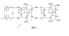
- FIG. 1 is a schematic diagram of a differential (i.e. push-pull) multistage amplifier MMIC 10 for a LDMOS amplifier according to an embodiment of the invention.
- the circuit 10 is a driver circuit for a 55dBm P3dB final stage with 19dB small signal gain.
- the circuit 10 differs from a conventional LDMOS amplifier in that is comprises a high resistivity substrate and ground connections that are split into: AC ground connections; and DC ground connections.
- the AC ground connections are virtual grounds due to the differential operation of the circuit, whereas the DC ground connections (which can experience parasitic inductance) are realised using physical grounding electrical connections (such as wire bond connections or a microstrip-like connection, for example).
- the embodiment of Figure 1 makes use of the realisation that for a differential amplifier circuit the AC (e.g. Radio Frequency) and DC ground connections can be split (e.g. provided separately from each other), thus enabling the AC ground connections to be provided by virtual grounds and the DC ground connections can be obtained with physical (inductive) connections.
- the AC (e.g. Radio Frequency) and DC ground connections can be split (e.g. provided separately from each other), thus enabling the AC ground connections to be provided by virtual grounds and the DC ground connections can be obtained with physical (inductive) connections.
- circuit 10 of Figure 1 resides between the source of the source-connected transistors LDMOS1, LDMOS2 and LDMOS3 & LDMOS4. More specifically, this is the location in the circuit where the split between the DC and AC grounding connections is implemented.
- a source to source connection of LDMOS1 and LDMOS2 is therefore implemented using an intermediate layer of metal to connect the source of LDMOS1 to the source of LDMOS2 such that the mid-point becomes a virtual AC ground VG due to the differential operation of the amplifier circuit.
- LDMOS3 and LDMOS4 connected to the source of LDMOS3 and LDMO4 is a second physical ground G2.
- the source of each of LDMOS3 and LDMOS4 is DC grounded, again in this example, using a plurality of wire bonds connections between source and ground.
- a source to source connection of LDMOS3 and LDMOS4 is also implemented using an intermediate layer of metal to connect the source of LDMOS3 to the source of LDMOS4 such that the mid-point becomes a virtual AC ground VG due to differential operation.
- FIG. 2 there is shown a plan view of a MMIC amplifier circuit according to an embodiment of the invention.
- DC grounding connection of the field-effect transistors is provided by a plurality of wire bond connections 50. This grounding arrangement provides a short connecting inductance to the amplifier circuit.
- the DC grounding connection for the amplifier circuit may be provided via a large microstrip-like connection which has low impedance, and hence a small inductance in the pH range.
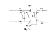
- Figure 3 is a schematic diagram of a final stage differential (i.e. push-pull) amplifier circuit 100 for a LDMOS amplifier according to an embodiment of the invention.
- the circuit 100 is final stage push-pull amplifier: P3dB 55dBm / 16dB at P3dB.
- the RF ground which is provided by virtual ground(s) from the differential operation of the circuit
- the DC ground which is provided by a physical grounding connection.
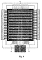
- FIG. 4 there is shown a schematic plan view of packaged amplifier circuit according to an embodiment of the invention, wherein the packaging is removed to show the circuit and wire bond connections.
- DC grounding connection of the field-effect transistors is provided by a plurality of wire bond connections 150 connected to grounding pads of the circuit. This grounding arrangement provides a short connecting inductance to the amplifier circuit.
- Figure 5A is a graph illustrating a variation of the inductors Q with operating frequency for various conventional amplifier circuits employing a low resistivity (10m ⁇ .cm) substrate (labelled “LOW_R”) and for two amplifier circuits employing a high resistivity (1K ⁇ *cm) substrate (labelled "HIGH_R”) according to an embodiment of the invention. From Figure 5A it is seen that, across all operating frequencies, the amplifier circuits according to an embodiment of the invention have a higher Q value than the conventional amplifier circuits employing a low resistivity substrate. Indeed, for a given operating frequency, the amplifier circuits according to an embodiment of the invention have a Q value which is approximately twice that of the conventional amplifier circuits employing a low resistivity substrate.
- Figure 5B is a graph illustrating a variation of the series inductance with operating frequency for various conventional amplifier circuits employing a low resistivity (10m ⁇ .cm) substrate (labelled “LOW_R”) and for amplifier circuits employing a high resistivity (1K ⁇ *cm) substrate (labelled “HIGH_R”) according to an embodiment of the invention. From Figure 5B it is seen that, across all operating frequencies, the amplifier circuits according to an embodiment of the invention have a lower series inductance than the conventional amplifier circuits employing a low resistivity substrate.
- Figure 5C is a graph illustrating a variation of the series resistance with operating frequency for various conventional amplifier circuits employing a low resistivity (10m ⁇ .cm) substrate (labelled “LOW_R”) and for amplifier circuits employing a high resistivity (1K ⁇ *cm) substrate (labelled “HIGH_R”) according to an embodiment of the invention. From Figure 5C it is seen that, across all operating frequencies, the amplifier circuits according to an embodiment of the invention have a lower series resistance than the conventional amplifier circuits employing a low resistivity substrate.
Landscapes
- Engineering & Computer Science (AREA)
- Power Engineering (AREA)
- Amplifiers (AREA)
Abstract
Description
- This invention relates to the field of amplifier circuits, and more particularly to differential amplifier circuits for laterally diffused metal oxide semiconductor (LDMOS) amplifiers.
- LDMOS Power amplifier circuits are widely used in Radio Frequency (RF) applications. Conventional LDMOS devices (including LDMOS power amplifiers) typically employ a low resistivity substrate having a resistivity around or below 10 mΩ*cm. The usage of a low resistivity substrate limits LDMOS performance.
- Use of higher resistivity substrates can provide improvement in maximum frequency and power performance roll-off of an active LDMOS device and significant improvement in passive LDMOS devices (such as inductors and transmission lines, for example). Consequently, there has been a drive to employ higher resistivity substrates in LDMOS devices.
- However, known techniques for employing higher resistivity substrates in LDMOS devices require the use of thru-substrate vias for grounding connections to be made. Such vias are complicated and expensive to implement. Nonetheless, due to the performance benefits of employing higher resistivity substrates in LDMOS devices, considerable investment and development work has been undertaken (and is currently on going) in order to optimlse the use of such thru-substrate vias in higher resistivity substrates.
- According to an aspect of the invention there is provided a differential amplifier circuit for an LDMOS-based amplifier, the circuit comprising a high resistivity substrate and separate DC and AC ground connections.
- Proposed is a differential amplifier circuit that employs a high resistivity substrate. When compared to using a conventional low resistivity substrate, use of a high resistivity substrate provides an improvement in maximum frequency and power performance roll-off of an active device and significant improvement in passive devices (such as inductors and transmission lines, for example). Further, unlike conventional circuits that employ a high resistivity substrate, the proposed amplifier circuit may not require thru-substrate vias for ground connection. Embodiments may therefore enable the use of a high resistivity silicon substrate without the need for expensive thru-silicon via holes. Such embodiments may be useful for future generations of LDMOS technologies, especially since conventional LDMOS technologies are such that little improvement can currently be realised in active or passive devices due to RF losses in the low resistivity silicon substrates that are typically employed.
- For the purpose of improved understanding, high resistivity is considered as around 50Ω*cm or above, preferably 100Ω*cm or above, and even more preferably 1KΩ*cm or above. Conversely, low resistivity is considered to be around or below 10 mΩ*cm. Thus, embodiments may employ a high resistivity substrate having a resistivity that is several orders of magnitude greater than the resistivity (10 mΩ*cm or below) of a conventional low resistivity substrate.
- By enabling the use of a high resistivity silicon substrate without the need for thu-silicon via holes for ground connection(s), embodiments may reduce RF substrate losses whilst avoiding the need for complex and expensive thru-substrate via manufacturing
- Embodiments employing a high resistivity substrate may provide the following advantages:
- transistor roll-off improvement (higher Ft, constant power density and improved efficiency across a broader frequency range, e.g. extension of the current 1-2 GHz performance up to 3-4 GHz); and
- inductance and transmission lines drastic Q improvement.
- Embodiments may employ the concept of splitting the AC and DC grounding connections, wherein the AC ground connections are virtual grounds provided by the differential operation of the circuit, and wherein the DC ground connections physical grounding electrical connections. In this way, thru-substrate vias may not be required for grounding connections.
- In embodiment, the virtual ground connection may be provided by a source-to-source connection between two source-connected transistors.
- The high resistivity substrate may comprise silicon and may have a resistivity greater than or equal to 50 Ω*cm.
- According to an aspect of the invention there is provided a LDMOS-based amplifier comprising a differential amplifier circuit according to an embodiment of the invention.
- By way of example, an embodiment of the invention may be employed in an integrated circuit (IC), a monolithic microwave integrated circuit (MMIC), or a high-power RF amplifier circuit. Embodiments may therefore be used in a mobile base station or other devices/systems that may employ RF amplifier circuits, for example.
- Examples of the invention will now be described in detail with reference to the accompanying drawings, in which:
-
Figure 1 is a schematic diagram of a differential amplifier circuit for a LDMOS amplifier according to an embodiment of the invention; -
Figure 2 is a plan view of a MMIC amplifier circuit according to an embodiment of the invention; -
Figure 3 is a schematic diagram of a final stage differential (i.e. push-pull) amplifier circuit 100 for a LDMOS amplifier according to an embodiment of the invention; -
Figure 5A is a graph illustrating a variation of the inductors Q with operating frequency for various conventional amplifier circuits employing a low resistivity substrate and for two amplifier circuits employing a high resistivity substrate according to an embodiment of the invention; -
Figure 5B is a graph illustrating a variation of the series inductance with operating frequency for various conventional amplifier circuits employing a low resistivity substrate and for amplifier circuits employing a high resistivity substrate according to an embodiment of the invention; and -
Figure 5C is a graph illustrating a variation of the series resistance with operating frequency for various conventional amplifier circuits employing a low resistivity substrate and for amplifier circuits employing a high resistivity substrate according to an embodiment of the invention. -
Figure 1 is a schematic diagram of a differential (i.e. push-pull) multistage amplifier MMIC 10 for a LDMOS amplifier according to an embodiment of the invention. Here, thecircuit 10 is a driver circuit for a 55dBm P3dB final stage with 19dB small signal gain. - The
circuit 10 differs from a conventional LDMOS amplifier in that is comprises a high resistivity substrate and ground connections that are split into: AC ground connections; and DC ground connections. The AC ground connections are virtual grounds due to the differential operation of the circuit, whereas the DC ground connections (which can experience parasitic inductance) are realised using physical grounding electrical connections (such as wire bond connections or a microstrip-like connection, for example). - The embodiment of
Figure 1 makes use of the realisation that for a differential amplifier circuit the AC (e.g. Radio Frequency) and DC ground connections can be split (e.g. provided separately from each other), thus enabling the AC ground connections to be provided by virtual grounds and the DC ground connections can be obtained with physical (inductive) connections. By splitting the provision of the AC (e.g. Radio Frequency) and DC ground connections, thru-substrate vias are not required for grounding connections. - The notable feature of the
circuit 10 ofFigure 1 resides between the source of the source-connected transistors LDMOS1, LDMOS2 and LDMOS3 & LDMOS4. More specifically, this is the location in the circuit where the split between the DC and AC grounding connections is implemented. - Connected to the source of LDMOS1 and LDMOS2 is a first physical ground G1. Thus, the source of each of LDMOS1 and LDMOS2 is DC grounded and, in this example, the grounding connection is made using a plurality of wire bonds connections between source and ground. Such DC grounding connections do not work well for AC (e.g. RF) grounding due ot the associated inductance of the wire bonds connections. A source to source connection of LDMOS1 and LDMOS2 is therefore implemented using an intermediate layer of metal to connect the source of LDMOS1 to the source of LDMOS2 such that the mid-point becomes a virtual AC ground VG due to the differential operation of the amplifier circuit.
- Similarly, connected to the source of LDMOS3 and LDMO4 is a second physical ground G2. Thus, the source of each of LDMOS3 and LDMOS4 is DC grounded, again in this example, using a plurality of wire bonds connections between source and ground. A source to source connection of LDMOS3 and LDMOS4 is also implemented using an intermediate layer of metal to connect the source of LDMOS3 to the source of LDMOS4 such that the mid-point becomes a virtual AC ground VG due to differential operation.
- Turning to
Figure 2 , there is shown a plan view of a MMIC amplifier circuit according to an embodiment of the invention. DC grounding connection of the field-effect transistors is provided by a plurality ofwire bond connections 50. This grounding arrangement provides a short connecting inductance to the amplifier circuit. - In other embodiments, the DC grounding connection for the amplifier circuit may be provided via a large microstrip-like connection which has low impedance, and hence a small inductance in the pH range.
-
Figure 3 is a schematic diagram of a final stage differential (i.e. push-pull) amplifier circuit 100 for a LDMOS amplifier according to an embodiment of the invention. Here, the circuit 100 is final stage push-pull amplifier: P3dB 55dBm / 16dB at P3dB. - In the amplifier circuit, two sorts of ground connections are employed: the RF ground, which is provided by virtual ground(s) from the differential operation of the circuit; and the DC ground, which is provided by a physical grounding connection.
- Turning to
Figure 4 , there is shown a schematic plan view of packaged amplifier circuit according to an embodiment of the invention, wherein the packaging is removed to show the circuit and wire bond connections. DC grounding connection of the field-effect transistors is provided by a plurality ofwire bond connections 150 connected to grounding pads of the circuit. This grounding arrangement provides a short connecting inductance to the amplifier circuit. -
Figure 5A is a graph illustrating a variation of the inductors Q with operating frequency for various conventional amplifier circuits employing a low resistivity (10mΩ.cm) substrate (labelled "LOW_R") and for two amplifier circuits employing a high resistivity (1KΩ*cm) substrate (labelled "HIGH_R") according to an embodiment of the invention. FromFigure 5A it is seen that, across all operating frequencies, the amplifier circuits according to an embodiment of the invention have a higher Q value than the conventional amplifier circuits employing a low resistivity substrate. Indeed, for a given operating frequency, the amplifier circuits according to an embodiment of the invention have a Q value which is approximately twice that of the conventional amplifier circuits employing a low resistivity substrate. -
Figure 5B is a graph illustrating a variation of the series inductance with operating frequency for various conventional amplifier circuits employing a low resistivity (10mΩ.cm) substrate (labelled "LOW_R") and for amplifier circuits employing a high resistivity (1KΩ*cm) substrate (labelled "HIGH_R") according to an embodiment of the invention. FromFigure 5B it is seen that, across all operating frequencies, the amplifier circuits according to an embodiment of the invention have a lower series inductance than the conventional amplifier circuits employing a low resistivity substrate. -
Figure 5C is a graph illustrating a variation of the series resistance with operating frequency for various conventional amplifier circuits employing a low resistivity (10mΩ.cm) substrate (labelled "LOW_R") and for amplifier circuits employing a high resistivity (1KΩ*cm) substrate (labelled "HIGH_R") according to an embodiment of the invention. FromFigure 5C it is seen that, across all operating frequencies, the amplifier circuits according to an embodiment of the invention have a lower series resistance than the conventional amplifier circuits employing a low resistivity substrate. - From
Figures 5A-5C it will be seen that the series resistance and the series inductance of embodiments of the invention employing a high resistivity substrate is significantly reduced when compared to conventional amplifier circuits employing a low resistivity substrate. Embodiments employing the described concept of splitting the AC and DC ground connections may therefore provide improvement in the maximum frequency and power performance roll-off of an active device and significant improvement in passive devices (such as inductors and transmission lines, for example). Furthermore, such embodiments may not require thru-substrate vias for ground connection, thereby avoiding the need for expensive via fabrication processes. - Other variations to the disclosed embodiments can be understood and effected by those skilled in the art in practicing the claimed invention, from a study of the drawings, the disclosure, and the appended claims. In the claims, the word "comprising" does not exclude other elements or steps, and the indefinite article "a" or "an" does not exclude a plurality.
Claims (13)
- A differential amplifier circuit for an LDMOS-based amplifier, the circuit comprising a high resistivity substrate and separate DC and AC ground connections.
- The circuit of claim 1, wherein the AC ground connection comprises a virtual ground connection.
- The circuit of claim 2, wherein the circuit comprises first and second transistors, the source of the first transistor being electrically connected to the source of the second transistor by a source-to-source connection, and wherein the virtual ground connection is provided by the source-to-source connection.
- The circuit of claim 3, wherein the source-to-source connection is formed from an intermediate layer of metal.
- The circuit of any preceding claim, wherein the DC ground connection comprises a plurality of wire bond connections or a microstrip connection.
- The circuit of any preceding claim, wherein the high resistivity substrate comprises silicon.
- The circuit of any preceding claim, wherein the high resistivity substrate has a resistivity greater than 50 Ω*cm.
- The circuit of claim 7, wherein the high resistivity substrate has a resistivity greater than 100 Ω*cm.
- The circuit of claim 7, wherein the high resistivity substrate has a resistivity greater than or equal to 1 KΩ*cm.
- An LDMOS amplifier circuit comprising a differential amplifier circuit according to any preceding claim.
- A packaged high-power radio frequency, RF, amplifier circuit comprising:an amplifier circuit according to any preceding claim,.
- An integrated circuit comprising an amplifier circuit according to any preceding claim.
- A mobile base station comprising an amplifier circuit according to any of claims 1 to 11.
Priority Applications (3)
| Application Number | Priority Date | Filing Date | Title |
|---|---|---|---|
| EP13290190.1A EP2838194B1 (en) | 2013-08-14 | 2013-08-14 | Amplifier circuits |
| CN201410363787.8A CN104378072B (en) | 2013-08-14 | 2014-07-28 | Amplifier circuit |
| US14/444,063 US9041465B2 (en) | 2013-08-14 | 2014-07-28 | Amplifier circuits |
Applications Claiming Priority (1)
| Application Number | Priority Date | Filing Date | Title |
|---|---|---|---|
| EP13290190.1A EP2838194B1 (en) | 2013-08-14 | 2013-08-14 | Amplifier circuits |
Publications (2)
| Publication Number | Publication Date |
|---|---|
| EP2838194A1 true EP2838194A1 (en) | 2015-02-18 |
| EP2838194B1 EP2838194B1 (en) | 2017-10-04 |
Family
ID=49322300
Family Applications (1)
| Application Number | Title | Priority Date | Filing Date |
|---|---|---|---|
| EP13290190.1A Not-in-force EP2838194B1 (en) | 2013-08-14 | 2013-08-14 | Amplifier circuits |
Country Status (3)
| Country | Link |
|---|---|
| US (1) | US9041465B2 (en) |
| EP (1) | EP2838194B1 (en) |
| CN (1) | CN104378072B (en) |
Families Citing this family (10)
| Publication number | Priority date | Publication date | Assignee | Title |
|---|---|---|---|---|
| DE102015212152B4 (en) * | 2015-06-30 | 2018-03-15 | TRUMPF Hüttinger GmbH + Co. KG | Non-linear radio frequency amplifier arrangement |
| JP6923119B2 (en) | 2017-10-24 | 2021-08-18 | 住友電工デバイス・イノベーション株式会社 | Semiconductor amplifier |
| US10630285B1 (en) | 2017-11-21 | 2020-04-21 | Transphorm Technology, Inc. | Switching circuits having drain connected ferrite beads |
| US10756207B2 (en) | 2018-10-12 | 2020-08-25 | Transphorm Technology, Inc. | Lateral III-nitride devices including a vertical gate module |
| WO2020191357A1 (en) | 2019-03-21 | 2020-09-24 | Transphorm Technology, Inc. | Integrated design for iii-nitride devices |
| US11050395B2 (en) | 2019-11-04 | 2021-06-29 | Nxp Usa, Inc. | Radio frequency (RF) amplifier |
| US11749656B2 (en) | 2020-06-16 | 2023-09-05 | Transphorm Technology, Inc. | Module configurations for integrated III-Nitride devices |
| CN116325158A (en) | 2020-08-05 | 2023-06-23 | 创世舫科技有限公司 | III-Nitride Devices Including Depletion Layers |
| WO2022061181A1 (en) | 2020-09-21 | 2022-03-24 | Transphorm Technology, Inc. | Iii-nitride devices with through-via structures |
| US12451468B1 (en) | 2021-08-25 | 2025-10-21 | Transphorm Technology, Inc. | III-N devices with improved reliability |
Citations (6)
| Publication number | Priority date | Publication date | Assignee | Title |
|---|---|---|---|---|
| US20020145184A1 (en) * | 2001-04-05 | 2002-10-10 | Ericsson Inc. | Single chip push-pull power transistor device |
| US20050083133A1 (en) * | 2003-10-15 | 2005-04-21 | Sharp Kabushiki Kaisha | Balanced amplifier circuit and high-frequency communication apparatus |
| EP1748487A2 (en) * | 2005-07-26 | 2007-01-31 | Infineon Tehnologies AG | Semiconductor power device and RF signal amplifier |
| WO2010038111A1 (en) * | 2008-09-30 | 2010-04-08 | Freescale Semiconductor, Inc. | Wireless communication device and semiconductor package device having a power amplifier therefor |
| WO2010125431A1 (en) * | 2009-04-30 | 2010-11-04 | Freescale Semiconductor, Inc. | Wireless communication device and semiconductor package device having a power amplifier therefor |
| EP2600525A2 (en) * | 2009-04-30 | 2013-06-05 | Freescale Semiconductor, Inc. | Wireless communication device and semiconductor package device having a power amplifier therefor |
Family Cites Families (2)
| Publication number | Priority date | Publication date | Assignee | Title |
|---|---|---|---|---|
| JP4545548B2 (en) * | 2004-10-21 | 2010-09-15 | ルネサスエレクトロニクス株式会社 | Semiconductor integrated circuit and semiconductor device |
| JP5247367B2 (en) * | 2008-11-13 | 2013-07-24 | ルネサスエレクトロニクス株式会社 | RF power amplifier |
-
2013
- 2013-08-14 EP EP13290190.1A patent/EP2838194B1/en not_active Not-in-force
-
2014
- 2014-07-28 CN CN201410363787.8A patent/CN104378072B/en not_active Expired - Fee Related
- 2014-07-28 US US14/444,063 patent/US9041465B2/en not_active Expired - Fee Related
Patent Citations (6)
| Publication number | Priority date | Publication date | Assignee | Title |
|---|---|---|---|---|
| US20020145184A1 (en) * | 2001-04-05 | 2002-10-10 | Ericsson Inc. | Single chip push-pull power transistor device |
| US20050083133A1 (en) * | 2003-10-15 | 2005-04-21 | Sharp Kabushiki Kaisha | Balanced amplifier circuit and high-frequency communication apparatus |
| EP1748487A2 (en) * | 2005-07-26 | 2007-01-31 | Infineon Tehnologies AG | Semiconductor power device and RF signal amplifier |
| WO2010038111A1 (en) * | 2008-09-30 | 2010-04-08 | Freescale Semiconductor, Inc. | Wireless communication device and semiconductor package device having a power amplifier therefor |
| WO2010125431A1 (en) * | 2009-04-30 | 2010-11-04 | Freescale Semiconductor, Inc. | Wireless communication device and semiconductor package device having a power amplifier therefor |
| EP2600525A2 (en) * | 2009-04-30 | 2013-06-05 | Freescale Semiconductor, Inc. | Wireless communication device and semiconductor package device having a power amplifier therefor |
Also Published As
| Publication number | Publication date |
|---|---|
| CN104378072A (en) | 2015-02-25 |
| US9041465B2 (en) | 2015-05-26 |
| US20150048884A1 (en) | 2015-02-19 |
| CN104378072B (en) | 2017-08-11 |
| EP2838194B1 (en) | 2017-10-04 |
Similar Documents
| Publication | Publication Date | Title |
|---|---|---|
| US9041465B2 (en) | Amplifier circuits | |
| EP3799303B1 (en) | Compact three-way doherty amplifier module | |
| EP3247038B1 (en) | Multiple-path rf amplifiers with angularly offset signal path directions, and methods of manufacture thereof | |
| EP3331161B1 (en) | Amplifier die with elongated side pads, and amplifier modules that incorporate such amplifier die | |
| US10903182B1 (en) | Amplifier die bond pad design and amplifier die arrangement for compact Doherty amplifier modules | |
| JP6316512B1 (en) | Semiconductor device | |
| CN108206677B (en) | Multi-baseband termination assembly for RF power amplifier with enhanced video bandwidth | |
| CN102332438B (en) | Inductive bond-wire circuit | |
| EP3544178A1 (en) | Amplifier device with harmonic termination circuit | |
| CN109585561B (en) | Transistor die with drain via arrangement and method of manufacturing same | |
| EP3460843B1 (en) | Transistor with shield structure, packaged device, and method of manufacture | |
| TW201832461A (en) | 90 degree lumped and decentralized Duch impedance inverter | |
| US9503030B2 (en) | Radio frequency power amplifier | |
| JP4313759B2 (en) | Hybrid structure for distributed power amplifiers. | |
| US11302659B2 (en) | Semiconductor device | |
| US8848394B2 (en) | Radio frequency circuit with impedance matching | |
| US11979117B2 (en) | High frequency semiconductor amplifier | |
| US10115697B2 (en) | Coupling element, integrated circuit device and method of fabrication therefor | |
| EP3493257B1 (en) | Silicon shielding for baseband termination and rf performance enhancement | |
| JP2025005416A (en) | Output matching network for reducing self and mutual inductance of output inductive components in a cavity package | |
| Gruner et al. | Fully integrated 5.6–6.4 GHz power amplifier using transformer combining | |
| Li et al. | A high-frequency power amplifier using GaN power cell technology | |
| JP2006093500A (en) | Electronic equipment |
Legal Events
| Date | Code | Title | Description |
|---|---|---|---|
| 17P | Request for examination filed |
Effective date: 20140326 |
|
| AK | Designated contracting states |
Kind code of ref document: A1 Designated state(s): AL AT BE BG CH CY CZ DE DK EE ES FI FR GB GR HR HU IE IS IT LI LT LU LV MC MK MT NL NO PL PT RO RS SE SI SK SM TR |
|
| AX | Request for extension of the european patent |
Extension state: BA ME |
|
| PUAI | Public reference made under article 153(3) epc to a published international application that has entered the european phase |
Free format text: ORIGINAL CODE: 0009012 |
|
| 17Q | First examination report despatched |
Effective date: 20150313 |
|
| RBV | Designated contracting states (corrected) |
Designated state(s): AL AT BE BG CH CY CZ DE DK EE ES FI FR GB GR HR HU IE IS IT LI LT LU LV MC MK MT NL NO PL PT RO RS SE SI SK SM TR |
|
| RAP1 | Party data changed (applicant data changed or rights of an application transferred) |
Owner name: SAMBA HOLDCO NETHERLANDS B.V. |
|
| RAP1 | Party data changed (applicant data changed or rights of an application transferred) |
Owner name: AMPLEON NETHERLANDS B.V. |
|
| GRAP | Despatch of communication of intention to grant a patent |
Free format text: ORIGINAL CODE: EPIDOSNIGR1 |
|
| INTG | Intention to grant announced |
Effective date: 20170421 |
|
| GRAS | Grant fee paid |
Free format text: ORIGINAL CODE: EPIDOSNIGR3 |
|
| GRAA | (expected) grant |
Free format text: ORIGINAL CODE: 0009210 |
|
| AK | Designated contracting states |
Kind code of ref document: B1 Designated state(s): AL AT BE BG CH CY CZ DE DK EE ES FI FR GB GR HR HU IE IS IT LI LT LU LV MC MK MT NL NO PL PT RO RS SE SI SK SM TR |
|
| REG | Reference to a national code |
Ref country code: GB Ref legal event code: FG4D |
|
| REG | Reference to a national code |
Ref country code: CH Ref legal event code: EP |
|
| REG | Reference to a national code |
Ref country code: AT Ref legal event code: REF Ref document number: 934905 Country of ref document: AT Kind code of ref document: T Effective date: 20171015 |
|
| REG | Reference to a national code |
Ref country code: IE Ref legal event code: FG4D |
|
| REG | Reference to a national code |
Ref country code: DE Ref legal event code: R096 Ref document number: 602013027412 Country of ref document: DE |
|
| REG | Reference to a national code |
Ref country code: NL Ref legal event code: FP |
|
| REG | Reference to a national code |
Ref country code: LT Ref legal event code: MG4D |
|
| REG | Reference to a national code |
Ref country code: AT Ref legal event code: MK05 Ref document number: 934905 Country of ref document: AT Kind code of ref document: T Effective date: 20171004 |
|
| PG25 | Lapsed in a contracting state [announced via postgrant information from national office to epo] |
Ref country code: SE Free format text: LAPSE BECAUSE OF FAILURE TO SUBMIT A TRANSLATION OF THE DESCRIPTION OR TO PAY THE FEE WITHIN THE PRESCRIBED TIME-LIMIT Effective date: 20171004 Ref country code: FI Free format text: LAPSE BECAUSE OF FAILURE TO SUBMIT A TRANSLATION OF THE DESCRIPTION OR TO PAY THE FEE WITHIN THE PRESCRIBED TIME-LIMIT Effective date: 20171004 Ref country code: NO Free format text: LAPSE BECAUSE OF FAILURE TO SUBMIT A TRANSLATION OF THE DESCRIPTION OR TO PAY THE FEE WITHIN THE PRESCRIBED TIME-LIMIT Effective date: 20180104 Ref country code: LT Free format text: LAPSE BECAUSE OF FAILURE TO SUBMIT A TRANSLATION OF THE DESCRIPTION OR TO PAY THE FEE WITHIN THE PRESCRIBED TIME-LIMIT Effective date: 20171004 Ref country code: ES Free format text: LAPSE BECAUSE OF FAILURE TO SUBMIT A TRANSLATION OF THE DESCRIPTION OR TO PAY THE FEE WITHIN THE PRESCRIBED TIME-LIMIT Effective date: 20171004 |
|
| PG25 | Lapsed in a contracting state [announced via postgrant information from national office to epo] |
Ref country code: HR Free format text: LAPSE BECAUSE OF FAILURE TO SUBMIT A TRANSLATION OF THE DESCRIPTION OR TO PAY THE FEE WITHIN THE PRESCRIBED TIME-LIMIT Effective date: 20171004 Ref country code: BG Free format text: LAPSE BECAUSE OF FAILURE TO SUBMIT A TRANSLATION OF THE DESCRIPTION OR TO PAY THE FEE WITHIN THE PRESCRIBED TIME-LIMIT Effective date: 20180104 Ref country code: AT Free format text: LAPSE BECAUSE OF FAILURE TO SUBMIT A TRANSLATION OF THE DESCRIPTION OR TO PAY THE FEE WITHIN THE PRESCRIBED TIME-LIMIT Effective date: 20171004 Ref country code: GR Free format text: LAPSE BECAUSE OF FAILURE TO SUBMIT A TRANSLATION OF THE DESCRIPTION OR TO PAY THE FEE WITHIN THE PRESCRIBED TIME-LIMIT Effective date: 20180105 Ref country code: LV Free format text: LAPSE BECAUSE OF FAILURE TO SUBMIT A TRANSLATION OF THE DESCRIPTION OR TO PAY THE FEE WITHIN THE PRESCRIBED TIME-LIMIT Effective date: 20171004 Ref country code: RS Free format text: LAPSE BECAUSE OF FAILURE TO SUBMIT A TRANSLATION OF THE DESCRIPTION OR TO PAY THE FEE WITHIN THE PRESCRIBED TIME-LIMIT Effective date: 20171004 Ref country code: IS Free format text: LAPSE BECAUSE OF FAILURE TO SUBMIT A TRANSLATION OF THE DESCRIPTION OR TO PAY THE FEE WITHIN THE PRESCRIBED TIME-LIMIT Effective date: 20180204 |
|
| REG | Reference to a national code |
Ref country code: DE Ref legal event code: R097 Ref document number: 602013027412 Country of ref document: DE |
|
| PG25 | Lapsed in a contracting state [announced via postgrant information from national office to epo] |
Ref country code: CZ Free format text: LAPSE BECAUSE OF FAILURE TO SUBMIT A TRANSLATION OF THE DESCRIPTION OR TO PAY THE FEE WITHIN THE PRESCRIBED TIME-LIMIT Effective date: 20171004 Ref country code: DK Free format text: LAPSE BECAUSE OF FAILURE TO SUBMIT A TRANSLATION OF THE DESCRIPTION OR TO PAY THE FEE WITHIN THE PRESCRIBED TIME-LIMIT Effective date: 20171004 Ref country code: EE Free format text: LAPSE BECAUSE OF FAILURE TO SUBMIT A TRANSLATION OF THE DESCRIPTION OR TO PAY THE FEE WITHIN THE PRESCRIBED TIME-LIMIT Effective date: 20171004 Ref country code: SK Free format text: LAPSE BECAUSE OF FAILURE TO SUBMIT A TRANSLATION OF THE DESCRIPTION OR TO PAY THE FEE WITHIN THE PRESCRIBED TIME-LIMIT Effective date: 20171004 |
|
| PLBE | No opposition filed within time limit |
Free format text: ORIGINAL CODE: 0009261 |
|
| STAA | Information on the status of an ep patent application or granted ep patent |
Free format text: STATUS: NO OPPOSITION FILED WITHIN TIME LIMIT |
|
| REG | Reference to a national code |
Ref country code: FR Ref legal event code: PLFP Year of fee payment: 6 |
|
| PG25 | Lapsed in a contracting state [announced via postgrant information from national office to epo] |
Ref country code: RO Free format text: LAPSE BECAUSE OF FAILURE TO SUBMIT A TRANSLATION OF THE DESCRIPTION OR TO PAY THE FEE WITHIN THE PRESCRIBED TIME-LIMIT Effective date: 20171004 Ref country code: PL Free format text: LAPSE BECAUSE OF FAILURE TO SUBMIT A TRANSLATION OF THE DESCRIPTION OR TO PAY THE FEE WITHIN THE PRESCRIBED TIME-LIMIT Effective date: 20171004 Ref country code: SM Free format text: LAPSE BECAUSE OF FAILURE TO SUBMIT A TRANSLATION OF THE DESCRIPTION OR TO PAY THE FEE WITHIN THE PRESCRIBED TIME-LIMIT Effective date: 20171004 Ref country code: IT Free format text: LAPSE BECAUSE OF FAILURE TO SUBMIT A TRANSLATION OF THE DESCRIPTION OR TO PAY THE FEE WITHIN THE PRESCRIBED TIME-LIMIT Effective date: 20171004 |
|
| 26N | No opposition filed |
Effective date: 20180705 |
|
| PG25 | Lapsed in a contracting state [announced via postgrant information from national office to epo] |
Ref country code: SI Free format text: LAPSE BECAUSE OF FAILURE TO SUBMIT A TRANSLATION OF THE DESCRIPTION OR TO PAY THE FEE WITHIN THE PRESCRIBED TIME-LIMIT Effective date: 20171004 |
|
| PG25 | Lapsed in a contracting state [announced via postgrant information from national office to epo] |
Ref country code: MC Free format text: LAPSE BECAUSE OF FAILURE TO SUBMIT A TRANSLATION OF THE DESCRIPTION OR TO PAY THE FEE WITHIN THE PRESCRIBED TIME-LIMIT Effective date: 20171004 |
|
| REG | Reference to a national code |
Ref country code: CH Ref legal event code: PL |
|
| PG25 | Lapsed in a contracting state [announced via postgrant information from national office to epo] |
Ref country code: CH Free format text: LAPSE BECAUSE OF NON-PAYMENT OF DUE FEES Effective date: 20180831 Ref country code: LU Free format text: LAPSE BECAUSE OF NON-PAYMENT OF DUE FEES Effective date: 20180814 Ref country code: LI Free format text: LAPSE BECAUSE OF NON-PAYMENT OF DUE FEES Effective date: 20180831 |
|
| REG | Reference to a national code |
Ref country code: BE Ref legal event code: MM Effective date: 20180831 |
|
| PG25 | Lapsed in a contracting state [announced via postgrant information from national office to epo] |
Ref country code: BE Free format text: LAPSE BECAUSE OF NON-PAYMENT OF DUE FEES Effective date: 20180831 |
|
| PG25 | Lapsed in a contracting state [announced via postgrant information from national office to epo] |
Ref country code: MT Free format text: LAPSE BECAUSE OF NON-PAYMENT OF DUE FEES Effective date: 20180814 |
|
| PG25 | Lapsed in a contracting state [announced via postgrant information from national office to epo] |
Ref country code: TR Free format text: LAPSE BECAUSE OF FAILURE TO SUBMIT A TRANSLATION OF THE DESCRIPTION OR TO PAY THE FEE WITHIN THE PRESCRIBED TIME-LIMIT Effective date: 20171004 |
|
| PG25 | Lapsed in a contracting state [announced via postgrant information from national office to epo] |
Ref country code: PT Free format text: LAPSE BECAUSE OF FAILURE TO SUBMIT A TRANSLATION OF THE DESCRIPTION OR TO PAY THE FEE WITHIN THE PRESCRIBED TIME-LIMIT Effective date: 20171004 Ref country code: HU Free format text: LAPSE BECAUSE OF FAILURE TO SUBMIT A TRANSLATION OF THE DESCRIPTION OR TO PAY THE FEE WITHIN THE PRESCRIBED TIME-LIMIT; INVALID AB INITIO Effective date: 20130814 |
|
| PG25 | Lapsed in a contracting state [announced via postgrant information from national office to epo] |
Ref country code: CY Free format text: LAPSE BECAUSE OF FAILURE TO SUBMIT A TRANSLATION OF THE DESCRIPTION OR TO PAY THE FEE WITHIN THE PRESCRIBED TIME-LIMIT Effective date: 20171004 Ref country code: MK Free format text: LAPSE BECAUSE OF NON-PAYMENT OF DUE FEES Effective date: 20171004 |
|
| PG25 | Lapsed in a contracting state [announced via postgrant information from national office to epo] |
Ref country code: AL Free format text: LAPSE BECAUSE OF FAILURE TO SUBMIT A TRANSLATION OF THE DESCRIPTION OR TO PAY THE FEE WITHIN THE PRESCRIBED TIME-LIMIT Effective date: 20171004 |
|
| PGFP | Annual fee paid to national office [announced via postgrant information from national office to epo] |
Ref country code: NL Payment date: 20210826 Year of fee payment: 9 |
|
| PGFP | Annual fee paid to national office [announced via postgrant information from national office to epo] |
Ref country code: FR Payment date: 20210825 Year of fee payment: 9 Ref country code: IE Payment date: 20210827 Year of fee payment: 9 |
|
| PGFP | Annual fee paid to national office [announced via postgrant information from national office to epo] |
Ref country code: DE Payment date: 20210827 Year of fee payment: 9 Ref country code: GB Payment date: 20210827 Year of fee payment: 9 |
|
| REG | Reference to a national code |
Ref country code: DE Ref legal event code: R119 Ref document number: 602013027412 Country of ref document: DE |
|
| REG | Reference to a national code |
Ref country code: NL Ref legal event code: MM Effective date: 20220901 |
|
| GBPC | Gb: european patent ceased through non-payment of renewal fee |
Effective date: 20220814 |
|
| PG25 | Lapsed in a contracting state [announced via postgrant information from national office to epo] |
Ref country code: NL Free format text: LAPSE BECAUSE OF NON-PAYMENT OF DUE FEES Effective date: 20220901 |
|
| PG25 | Lapsed in a contracting state [announced via postgrant information from national office to epo] |
Ref country code: IE Free format text: LAPSE BECAUSE OF NON-PAYMENT OF DUE FEES Effective date: 20220814 Ref country code: FR Free format text: LAPSE BECAUSE OF NON-PAYMENT OF DUE FEES Effective date: 20220831 Ref country code: DE Free format text: LAPSE BECAUSE OF NON-PAYMENT OF DUE FEES Effective date: 20230301 |
|
| PG25 | Lapsed in a contracting state [announced via postgrant information from national office to epo] |
Ref country code: GB Free format text: LAPSE BECAUSE OF NON-PAYMENT OF DUE FEES Effective date: 20220814 |