EP2833545A1 - Device and method for oscillation margin testing of a crystal oscillator - Google Patents
Device and method for oscillation margin testing of a crystal oscillator Download PDFInfo
- Publication number
- EP2833545A1 EP2833545A1 EP13290180.2A EP13290180A EP2833545A1 EP 2833545 A1 EP2833545 A1 EP 2833545A1 EP 13290180 A EP13290180 A EP 13290180A EP 2833545 A1 EP2833545 A1 EP 2833545A1
- Authority
- EP
- European Patent Office
- Prior art keywords
- oscillator
- circuit
- crystal
- variable resistor
- value
- Prior art date
- Legal status (The legal status is an assumption and is not a legal conclusion. Google has not performed a legal analysis and makes no representation as to the accuracy of the status listed.)
- Withdrawn
Links
- 239000013078 crystal Substances 0.000 title claims abstract description 64
- 230000010355 oscillation Effects 0.000 title claims abstract description 28
- 238000012360 testing method Methods 0.000 title claims description 32
- 238000000034 method Methods 0.000 title claims description 4
- 239000003990 capacitor Substances 0.000 claims description 13
- 238000004891 communication Methods 0.000 claims description 5
- 238000010998 test method Methods 0.000 claims description 3
- 230000008878 coupling Effects 0.000 claims description 2
- 238000010168 coupling process Methods 0.000 claims description 2
- 238000005859 coupling reaction Methods 0.000 claims description 2
- 238000013459 approach Methods 0.000 description 4
- 230000010363 phase shift Effects 0.000 description 3
- 238000013461 design Methods 0.000 description 2
- 238000001514 detection method Methods 0.000 description 2
- 239000010453 quartz Substances 0.000 description 2
- VYPSYNLAJGMNEJ-UHFFFAOYSA-N silicon dioxide Inorganic materials O=[Si]=O VYPSYNLAJGMNEJ-UHFFFAOYSA-N 0.000 description 2
- 230000002459 sustained effect Effects 0.000 description 2
- 230000007423 decrease Effects 0.000 description 1
- 230000001419 dependent effect Effects 0.000 description 1
- 239000013081 microcrystal Substances 0.000 description 1
- 238000012986 modification Methods 0.000 description 1
- 230000004048 modification Effects 0.000 description 1
- 229910052710 silicon Inorganic materials 0.000 description 1
- 239000010703 silicon Substances 0.000 description 1
Images



Classifications
-
- H—ELECTRICITY
- H03—ELECTRONIC CIRCUITRY
- H03B—GENERATION OF OSCILLATIONS, DIRECTLY OR BY FREQUENCY-CHANGING, BY CIRCUITS EMPLOYING ACTIVE ELEMENTS WHICH OPERATE IN A NON-SWITCHING MANNER; GENERATION OF NOISE BY SUCH CIRCUITS
- H03B5/00—Generation of oscillations using amplifier with regenerative feedback from output to input
- H03B5/30—Generation of oscillations using amplifier with regenerative feedback from output to input with frequency-determining element being electromechanical resonator
- H03B5/32—Generation of oscillations using amplifier with regenerative feedback from output to input with frequency-determining element being electromechanical resonator being a piezoelectric resonator
- H03B5/36—Generation of oscillations using amplifier with regenerative feedback from output to input with frequency-determining element being electromechanical resonator being a piezoelectric resonator active element in amplifier being semiconductor device
- H03B5/366—Generation of oscillations using amplifier with regenerative feedback from output to input with frequency-determining element being electromechanical resonator being a piezoelectric resonator active element in amplifier being semiconductor device and comprising means for varying the frequency by a variable voltage or current
-
- H—ELECTRICITY
- H03—ELECTRONIC CIRCUITRY
- H03B—GENERATION OF OSCILLATIONS, DIRECTLY OR BY FREQUENCY-CHANGING, BY CIRCUITS EMPLOYING ACTIVE ELEMENTS WHICH OPERATE IN A NON-SWITCHING MANNER; GENERATION OF NOISE BY SUCH CIRCUITS
- H03B2201/00—Aspects of oscillators relating to varying the frequency of the oscillations
- H03B2201/02—Varying the frequency of the oscillations by electronic means
Definitions
- This invention relates to the testing of a crystal oscillator.
- a crystal oscillator typically comprises an oscillator drive circuit and an oscillator crystal which is connected to the drive circuit.
- the drive circuit provides a feedback path around the oscillator to provide the required oscillation.
- the crystal needs to be matched with the drive circuit in order to obtain stable oscillation. A poor match can result in a number of problems including start-up problems, insufficient drive frequency stability and even halting of the oscillation.
- crystal oscillator is a Pierce oscillator circuit. This is a well-known circuit and is widely used for its excellent frequency stability and the wide range of frequencies over which it can be used.
- testing the oscillator performance is required to check if the oscillator gain margin is sufficient to allow crystal start-up and operation under all conditions and not too high so as to avoid crystal damage.
- an integrated oscillator drive circuit for coupling to an oscillator crystal comprising:
- This circuit provides a test circuit integrated with the oscillator drive circuit, which controls a variable resistor to enable the oscillator characteristics to be determined.
- the detection is essentially based on a negative resistance test, and by embedding this into the integrated circuit providing the drive function, the negative resistance check can be performed in a customer application, without changing the PCB layout. This provides a lower effort for the end-customer when designing a system using the oscillator circuit.
- the feedback network can comprise a fixed feedback resistor and the variable resistor.
- the fixed resistor provides the oscillator feedback function and the variable resistor provides the test function.
- the circuit can comprise a third terminal.
- the fixed feedback resistor can be between the first and third terminals and the variable resistor can be between the second and third terminals. If the variable resistor is set to zero, the circuit becomes equivalent to the standard configuration, in that the second and third terminals are connected, so that the crystal oscillator and fixed feedback resistor are in parallel.
- the circuit essentially then has two terminals for connection to the oscillator crystal.
- the controller is adapted to set the value of the variable resistor to:
- the circuit becomes equivalent to a standard circuit.
- the first value or set of values in the test mode can for example include 3 times the effective series resistance of the oscillator crystal being used.
- the first value can for example be programmed by the end-customer to apply a test suitable for the particular oscillator crystal being used.
- the first value or set of values can (instead or additionally) include 5 times the effective series resistance of the oscillator crystal.
- the detector can comprise a peak detector for detecting the presence of oscillations.
- the invention also provides an oscillator comprising:
- This oscillator can be a Pierce oscillator.
- the oscillator further comprises first and second capacitors each connected between a respective side of the amplifier and ground.
- the capacitors can be part of a passive integrated circuit which is connected to the integrated oscillator drive circuit within a system-in-package.
- a trimmed capacitor can be used.
- the oscillator can be used in a near field communication system for generating a carrier frequency signal.
- the invention also provides a method of testing compatibility between an integrated oscillator drive circuit and an oscillator crystal, with the oscillator crystal connected to the drive circuit, comprising:
- the invention provides an integrated circuit for driving an oscillator, having an amplifier and a feedback network connected to the amplifier.
- the feedback network comprises a variable resistor.
- the circuit has first and second terminals for connection to the oscillator crystal, a controller for controlling a setting of the variable resistor and a detector for detecting oscillation for one or more variable resistor settings.
- This circuit thus provides an embedded system allowing the compatibility between an oscillator crystal and an integrated circuit used for driving the oscillator to be determined. This determination can be made for example in a customer application.
- FIG. 1 shows the known basic quartz crystal Pierce oscillator circuit.
- the circuit comprises the oscillator crystal 10 and a drive circuit.
- the drive circuit comprises an active integrated circuit 12 and a pair of capacitors C1, C2, which can be part of a passive integrated circuit or separate components.
- the active integrated circuit comprises an inverting amplifier 14 and a feedback network in the form of a resistor 16.
- the active integrated circuit 12 has two terminals which connect to the opposite sides of the oscillator crystal, and the capacitors.
- the oscillator crystal in combination with the two capacitors forms a band pass filter (with a pi configuration), which provides a 180 degree phase shift and a gain at the resonant frequency.
- the combination of the negative gain from the amplifier and the phase shift results in a positive overall loop gain, which gives rise to sustained oscillation.
- the oscillator amplifier provides gain in the form of negative resistance. When the total circuit resistance is zero or negative, the oscillator will oscillate. When total circuit resistance becomes positive, the oscillator will fail.
- Figure 2 shows a typical test configuration. As shown in Figure 2 , a variable resistance 20 with value R3 is inserted in series with the crystal and set to a minimum resistance. The oscillator is powered and allowed to start.
- R3 is slowly increased until the oscillator just fails.
- the resistor R3 is then removed from the circuit and measured.
- the resistance is then compared to the crystal effective series resistance (ESR) as specified by the crystal manufacturer.
- ESR crystal effective series resistance
- the measured value of R3 should be several times the crystal Effective Series Resistance in order to provide sufficient gain to start the oscillator under all conditions.
- most industrial applications seek a factor of 3, while automotive applications seek a factor of at least 5.
- This method requires reconfiguration of the oscillator circuitry, in particular it needs a change in the PCB layout of the end application in order to add a resistor in series with the crystal. For this reason, it is not suitable for testability of products in a customer application.
- the invention provides a built-in system which is easy to implement in an end-customer application.
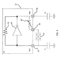
- Figure 3 shows an oscillator circuit in accordance with the invention, and shows schematically the fundamental change to the approach of Figure 2 .
- the circuit comprises a variable resistor 30 (again shown with resistance value R3) which is embedded into the active integrated circuit 12.
- the oscillation margin can be verified by using this embedded series resistor (on silicon).
- the active integrated circuit has an additional pin to allow the oscillator crystal to be connected differently to the capacitors.
- the circuit comprises first and second terminals 32, 34 for connection to the oscillator crystal and a third terminal 36.
- the fixed feedback resistor 16 is between the first and third terminals and thus in a feedback path around the amplifier 14, and the variable resistor 30 is between the second and third terminals 34,36.
- the capacitors connect to the first and third terminals.
- the value of the resistance is controlled and oscillation is detected for one or more variable resistor settings.
- Figure 4 shows a more detailed example of circuit implementation.
- the circuit again comprises first and second terminals 32, 34 for connection to the oscillator crystal and a third terminal 36.
- the fixed feedback resistor 16 is again between the first and third terminals 32,36 and the variable resistor 30 is between the second and third terminals 34,36.
- the capacitors connect to the first and second terminals.
- variable resistor is in series with the crystal defining a feedback path of the amplifier, in addition to the normal feedback path comprising a fixed resistor in parallel with the amplifier.
- R3 is set to non-zero values for a testing mode of operation.
- the capacitors C1, C2 are part of a passive integrated circuit 40 which is connected to the active integrated oscillator drive circuit 12 within a system-in-package 42.
- the connection 32 is split into two in Figure 4 , with one connection to the crystal oscillator and one to the capacitor passive IC 40.
- the oscillator crystal 10 is outside the system-in-package 42.
- the resistor R3 is set to a factor of 3 or 5 times the crystal Effective Series Resistance.
- a factor 5 is typically used for automotive applications.
- Figure 4 shows a multiplexer 44 which provides the control signal to the variable resistor 30.
- a test mode input controls the multiplexer 44, so when not in the test mode, the resistor is set to a zero value, and when in the test mode, the resistor is set to a desired value R, which can be programmed.
- the crystal oscillator is enabled and the start-up behaviour is studied.
- a peak detector 46 is used to measure a peak voltage on one terminal of the crystal. By comparing the peak voltage with a reference value Vref using comparator 48, oscillation can be detected. A signal Osc_ok is generated which indicates when oscillation is detected.
- the integrated oscillator drive circuit 12 is not compatible with the oscillator crystal ESR and the PCB layout.
- the integrated oscillator drive circuit is compatible with the crystal ESR and the PCB layout.
- the system allows programmable negative resistor testing.
- the resistor value can be changed by software in the end-customer application.
- the test can be for a single resistance value, or else multiple tests can be carried out for different resistance values (such as 3 times and 5 times the ESR of the crystal being used).
- NFC Near Field Communication
- An NFC system can for example be embedded in a mobile phone, and the NFC front end then needs its own 27.12MHz micro crystal with small thickness, and therefore with high ESR. This high crystal ESR decreases the ability of the oscillator circuit to start. Negative resistance testing is then required in the mobile phone application to check the compatibility between the NFC integrated crystal oscillator drive circuit , the application PCB layout and the crystal ESR.
- An analogue test bus can be embedded inside the circuit for controlling the test signals.
- the invention is of particular interest for Pierce oscillator configurations, because they provide a simple to design architecture. However, the invention can be applied to other oscillator designs which require matching of the crystal to the oscillator circuit.
- the example above is based on 27MHz oscillation.
- the decoupling capacitances are about 10-20pF.
- the detection of oscillation is based on a peak detector and comparator.
- clock detector which can be used to detect oscillations, and which are known in other circuits.
Landscapes
- Oscillators With Electromechanical Resonators (AREA)
Abstract
An integrated circuit for driving an oscillator has an amplifier and a feedback network connected to the amplifier. The feedback network comprises a variable resistor. The circuit has first and second terminals for connection to the oscillator crystal, a controller for controlling a setting of the variable resistor and a detector for detecting oscillation for one or more variable resistor settings.
This circuit thus provides an embedded system allowing the compatibility between an oscillator crystal and an integrated circuit used for driving the oscillator to be determined. This determination can be made for example in a customer application.
Description
- This invention relates to the testing of a crystal oscillator.
- A crystal oscillator typically comprises an oscillator drive circuit and an oscillator crystal which is connected to the drive circuit.
- The drive circuit provides a feedback path around the oscillator to provide the required oscillation. The crystal needs to be matched with the drive circuit in order to obtain stable oscillation. A poor match can result in a number of problems including start-up problems, insufficient drive frequency stability and even halting of the oscillation.
- One example of crystal oscillator is a Pierce oscillator circuit. This is a well-known circuit and is widely used for its excellent frequency stability and the wide range of frequencies over which it can be used.
- When designing a circuit for miniaturized quartz crystals, careful consideration must be given to the gain level of the drive circuit, and for this purpose it is required to check the match between the crystal and the drive circuit.
- In particular, testing the oscillator performance is required to check if the oscillator gain margin is sufficient to allow crystal start-up and operation under all conditions and not too high so as to avoid crystal damage.
- It is known to test the circuit function by measuring the circuit resistance, which needs to be negative for oscillations to be sustained. A known way to measure this resistance is by placing a variable resistor into the oscillator circuit. This variable resistor is external to the drive circuit, and the value of this resistor is tuned until the oscillation fails. The value of the tuned resistor then enables the circuit performance to determined, so that it can be determined if the oscillator will start up reliably and maintain stable oscillation, and this can be determined for different types of crystals and drive circuit.
- This approach requires the external circuit to be modified during a testing phase, which is inconvenient for a designer when implementing a circuit using the oscillator. For example, oscillation margin testing requires a specific PCB so cannot be performed in the final customer application.
- There is therefore a need for a testing approach which avoids the need for significant circuit modification as part of the test procedure.
- According to the invention, there is provided an integrated oscillator drive circuit for coupling to an oscillator crystal, comprising:
- an amplifier;
- a feedback network connected to the amplifier, wherein the feedback network comprises a variable resistor;
- first and second terminals for connection to the oscillator crystal;
- a controller for controlling a setting of the variable resistor; and
- a detector for detecting oscillation for one or more variable resistor settings.
- This circuit provides a test circuit integrated with the oscillator drive circuit, which controls a variable resistor to enable the oscillator characteristics to be determined.
- The detection is essentially based on a negative resistance test, and by embedding this into the integrated circuit providing the drive function, the negative resistance check can be performed in a customer application, without changing the PCB layout. This provides a lower effort for the end-customer when designing a system using the oscillator circuit.
- The feedback network can comprise a fixed feedback resistor and the variable resistor. The fixed resistor provides the oscillator feedback function and the variable resistor provides the test function.
- The circuit can comprise a third terminal. The fixed feedback resistor can be between the first and third terminals and the variable resistor can be between the second and third terminals. If the variable resistor is set to zero, the circuit becomes equivalent to the standard configuration, in that the second and third terminals are connected, so that the crystal oscillator and fixed feedback resistor are in parallel. The circuit essentially then has two terminals for connection to the oscillator crystal.
- The controller is adapted to set the value of the variable resistor to:
- a first value or set of values during a test mode;
- a zero value during a normal operation mode.
- Thus, in the normal operation mode, the circuit becomes equivalent to a standard circuit.
- The first value or set of values in the test mode can for example include 3 times the effective series resistance of the oscillator crystal being used. The first value can for example be programmed by the end-customer to apply a test suitable for the particular oscillator crystal being used. The first value or set of values can (instead or additionally) include 5 times the effective series resistance of the oscillator crystal.
- These values are the known measures to enable suitable stability and start-up performance to be determined.
- The detector can comprise a peak detector for detecting the presence of oscillations.
- The invention also provides an oscillator comprising:
- an integrated oscillator drive circuit of the invention; and
- an oscillator crystal connected between the first and second terminals.
- This oscillator can be a Pierce oscillator. For this configuration, the oscillator further comprises first and second capacitors each connected between a respective side of the amplifier and ground.
- The capacitors can be part of a passive integrated circuit which is connected to the integrated oscillator drive circuit within a system-in-package. A trimmed capacitor can be used.
- The oscillator can be used in a near field communication system for generating a carrier frequency signal.
- The invention also provides a method of testing compatibility between an integrated oscillator drive circuit and an oscillator crystal, with the oscillator crystal connected to the drive circuit, comprising:
- setting the value of a variable resistor, which forms part of a feedback network connected to an amplifier within the integrated oscillator drive circuit, to a first value or a set of first values;
- detecting oscillation for the one or more variable resistor settings; and
- setting the variable resistor to a zero value for subsequent normal operation of the integrated oscillator drive circuit and oscillator crystal.
- An example of the invention will now be described in detail with reference to the accompanying drawing, in which:
-
Figure 1 shows a known Pierce oscillator; -
Figure 2 shows a known way to test the suitability of the oscillator crystal with the oscillator circuit; -
Figure 3 shows in schematic form the approach of the invention for testing the suitability of the oscillator crystal with the oscillator circuit; and -
Figure 4 shows an oscillator circuit with the testing capability of the invention in more detail. - The invention provides an integrated circuit for driving an oscillator, having an amplifier and a feedback network connected to the amplifier. The feedback network comprises a variable resistor. The circuit has first and second terminals for connection to the oscillator crystal, a controller for controlling a setting of the variable resistor and a detector for detecting oscillation for one or more variable resistor settings.
- This circuit thus provides an embedded system allowing the compatibility between an oscillator crystal and an integrated circuit used for driving the oscillator to be determined. This determination can be made for example in a customer application.
-
Figure 1 shows the known basic quartz crystal Pierce oscillator circuit. The circuit comprises theoscillator crystal 10 and a drive circuit. The drive circuit comprises an activeintegrated circuit 12 and a pair of capacitors C1, C2, which can be part of a passive integrated circuit or separate components. The active integrated circuit comprises an invertingamplifier 14 and a feedback network in the form of aresistor 16. - The active
integrated circuit 12 has two terminals which connect to the opposite sides of the oscillator crystal, and the capacitors. - The oscillator crystal in combination with the two capacitors forms a band pass filter (with a pi configuration), which provides a 180 degree phase shift and a gain at the resonant frequency. The combination of the negative gain from the amplifier and the phase shift results in a positive overall loop gain, which gives rise to sustained oscillation.
- For oscillation to occur, the Barkhausen criteria must be met:
- the loop gain must be equal to or greater than one;
- the phase shift around the loop must be equal to an integral multiple of 2.
- While the crystal adds resistance to the oscillator circuit, the oscillator amplifier provides gain in the form of negative resistance. When the total circuit resistance is zero or negative, the oscillator will oscillate. When total circuit resistance becomes positive, the oscillator will fail.
- It is well known that negative resistance testing gives a measure of the oscillator gain margin and the ability of the oscillator circuit to start.
- Testing is performed at room temperature at a typical voltage.
-
Figure 2 shows a typical test configuration. As shown inFigure 2 , avariable resistance 20 with value R3 is inserted in series with the crystal and set to a minimum resistance. The oscillator is powered and allowed to start. - R3 is slowly increased until the oscillator just fails. The resistor R3 is then removed from the circuit and measured. The resistance is then compared to the crystal effective series resistance (ESR) as specified by the crystal manufacturer. The measured value of R3 should be several times the crystal Effective Series Resistance in order to provide sufficient gain to start the oscillator under all conditions. Typically, most industrial applications seek a factor of 3, while automotive applications seek a factor of at least 5.
- This method requires reconfiguration of the oscillator circuitry, in particular it needs a change in the PCB layout of the end application in order to add a resistor in series with the crystal. For this reason, it is not suitable for testability of products in a customer application.
- The invention provides a built-in system which is easy to implement in an end-customer application.
-
Figure 3 shows an oscillator circuit in accordance with the invention, and shows schematically the fundamental change to the approach ofFigure 2 . - The circuit comprises a variable resistor 30 (again shown with resistance value R3) which is embedded into the active
integrated circuit 12. - The oscillation margin can be verified by using this embedded series resistor (on silicon). The active integrated circuit has an additional pin to allow the oscillator crystal to be connected differently to the capacitors.
- In the example of
Figure 3 , the circuit comprises first andsecond terminals third terminal 36. The fixedfeedback resistor 16 is between the first and third terminals and thus in a feedback path around theamplifier 14, and thevariable resistor 30 is between the second andthird terminals - The value of the resistance is controlled and oscillation is detected for one or more variable resistor settings.
-
Figure 4 shows a more detailed example of circuit implementation. - In
Figure 4 , the circuit again comprises first andsecond terminals third terminal 36. The fixedfeedback resistor 16 is again between the first andthird terminals variable resistor 30 is between the second andthird terminals - The variable resistor is in series with the crystal defining a feedback path of the amplifier, in addition to the normal feedback path comprising a fixed resistor in parallel with the amplifier.
- When the value of R3 is set to zero, the circuit becomes equivalent to that shown in
Figure 2 . Thus, normal operation of the oscillator circuit can be obtained by setting R3=0. - R3 is set to non-zero values for a testing mode of operation.
- In the example of
Figure 4 , the capacitors C1, C2 are part of a passiveintegrated circuit 40 which is connected to the active integratedoscillator drive circuit 12 within a system-in-package 42. Thus, theconnection 32 is split into two inFigure 4 , with one connection to the crystal oscillator and one to the capacitorpassive IC 40. Theoscillator crystal 10 is outside the system-in-package 42. - To perform the negative resistance test in an industrial application, the resistor R3 is set to a factor of 3 or 5 times the crystal Effective Series Resistance. A factor 5 is typically used for automotive applications.
Figure 4 shows amultiplexer 44 which provides the control signal to thevariable resistor 30. A test mode input controls themultiplexer 44, so when not in the test mode, the resistor is set to a zero value, and when in the test mode, the resistor is set to a desired value R, which can be programmed. - When the resistor is set to the desired value R, the crystal oscillator is enabled and the start-up behaviour is studied.
- A
peak detector 46 is used to measure a peak voltage on one terminal of the crystal. By comparing the peak voltage with a reference valueVref using comparator 48, oscillation can be detected. A signal Osc_ok is generated which indicates when oscillation is detected. - If the Osc_ok signal is at ground, the integrated
oscillator drive circuit 12 is not compatible with the oscillator crystal ESR and the PCB layout. - If the Osc_ok signal is at the supply voltage level, the integrated oscillator drive circuit is compatible with the crystal ESR and the PCB layout.
- No dedicated PCB is required for performing the oscillation margin test by the end-customer. The negative resistance check can be performed in the customer application, without changing in the PCB layout, which gives lower effort for the end-customer.
- The system allows programmable negative resistor testing. The resistor value can be changed by software in the end-customer application.
- The test can be for a single resistance value, or else multiple tests can be carried out for different resistance values (such as 3 times and 5 times the ESR of the crystal being used).
- This invention is for example of interest in a Near Field Communication ("NFC") system. NFC is a new protocol of contactless communication in proximity distance, normalized by ISO18092. This communication is based on a 13.56MHz carrier frequency.
- An NFC system can for example be embedded in a mobile phone, and the NFC front end then needs its own 27.12MHz micro crystal with small thickness, and therefore with high ESR. This high crystal ESR decreases the ability of the oscillator circuit to start. Negative resistance testing is then required in the mobile phone application to check the compatibility between the NFC integrated crystal oscillator drive circuit , the application PCB layout and the crystal ESR.
- An analogue test bus can be embedded inside the circuit for controlling the test signals.
- The invention is of particular interest for Pierce oscillator configurations, because they provide a simple to design architecture. However, the invention can be applied to other oscillator designs which require matching of the crystal to the oscillator circuit.
- The example above is based on 27MHz oscillation. By way of example, the decoupling capacitances are about 10-20pF.
- In the example above, the detection of oscillation is based on a peak detector and comparator. There are other forms of clock detector which can be used to detect oscillations, and which are known in other circuits.
- The example above makes use of a multiplexer to control the variable resistor. There are of course other ways to control the resistor value, and the multiplexer function can be implemented as part of a processor which delivers a suitable output for controlling the variable resistor.
- Other variations to the disclosed embodiments can be understood and effected by those skilled in the art in practicing the claimed invention, from a study of the drawings, the disclosure, and the appended claims. In the claims, the word "comprising" does not exclude other elements or steps, and the indefinite article "a" or "an" does not exclude a plurality. The mere fact that certain measures are recited in mutually different dependent claims does not indicate that a combination of these measured cannot be used to advantage. Any reference signs in the claims should not be construed as limiting the scope.
Claims (14)
- An integrated oscillator drive circuit (42) for coupling to an oscillator crystal (10), comprising:an amplifier (14);a feedback network (16,30) connected to the amplifier, wherein the feedback network comprises a variable resistor (30);first and second terminals (32,34) for connection to the oscillator crystal;a controller (44) for controlling a setting of the variable resistor; anda detector (46,48) for detecting oscillation for one or more variable resistor settings.
- A circuit as claimed in claim 1, wherein the feedback network comprises a fixed feedback resistor (16) and the variable resistor (30).
- A circuit as claimed in claim 2, wherein the circuit comprises a third terminal (36), wherein the fixed feedback resistor (16) is between the first and third terminals (32,36) and the variable resistor (30) is between the second and third terminals (34,36).
- A circuit as claimed in any preceding claim, wherein the controller (44) is adapted, with the drive circuit coupled to an oscillator crystal, to set the value of the variable resistor to:a first value or set of values during a test mode;a zero value during a normal operation mode.
- A circuit as claimed in claim 4, wherein the first value or set of values includes 3 times the effective series resistance of the oscillator crystal.
- A circuit as claimed in claim 4 or 5, wherein the first value or set of values includes 5 times the effective series resistance of the oscillator crystal.
- A circuit as claimed in any preceding claim, wherein the detector comprises a peak detector (46) for detecting the presence of oscillations.
- An oscillator comprising:an integrated oscillator drive circuit (42) as claimed in any preceding claim; andan oscillator crystal (10) connected between the first and second terminals.
- A Pierce oscillator comprising an oscillator as claimed in claim 8, wherein the oscillator further comprises first and second capacitors (C1,C2) each connected between a respective side of the amplifier (14) and ground.
- An oscillator as claimed in claim 9, wherein the capacitors are part of a passive integrated circuit (40) which is connected to the integrated oscillator drive circuit (42) within a system-in-package.
- A near field communication system comprising an oscillator as claimed in claim 9 or 10 for generating a carrier frequency signal.
- A method of testing compatibility between an integrated oscillator drive circuit (42) and an oscillator crystal (10), with the oscillator crystal connected to the drive circuit, comprising:setting the value of a variable resistor (30), which forms part of a feedback network connected to an amplifier (14) within the integrated oscillator drive circuit, to a first value or a set of first values;detecting oscillation for the one or more variable resistor settings; andsetting the variable resistor to a zero value for subsequent normal operation of the integrated oscillator drive circuit and oscillator crystal.
- A method as claimed in claim 12, wherein the first value or set of values includes 3 times and/or 5 times the effective series resistance of the oscillator crystal.
- A method as claimed in claim 12 or 13, wherein detecting oscillations comprises using a peak detector for detecting the presence of oscillations.
Priority Applications (1)
| Application Number | Priority Date | Filing Date | Title |
|---|---|---|---|
| EP13290180.2A EP2833545A1 (en) | 2013-08-01 | 2013-08-01 | Device and method for oscillation margin testing of a crystal oscillator |
Applications Claiming Priority (1)
| Application Number | Priority Date | Filing Date | Title |
|---|---|---|---|
| EP13290180.2A EP2833545A1 (en) | 2013-08-01 | 2013-08-01 | Device and method for oscillation margin testing of a crystal oscillator |
Publications (1)
| Publication Number | Publication Date |
|---|---|
| EP2833545A1 true EP2833545A1 (en) | 2015-02-04 |
Family
ID=48985691
Family Applications (1)
| Application Number | Title | Priority Date | Filing Date |
|---|---|---|---|
| EP13290180.2A Withdrawn EP2833545A1 (en) | 2013-08-01 | 2013-08-01 | Device and method for oscillation margin testing of a crystal oscillator |
Country Status (1)
| Country | Link |
|---|---|
| EP (1) | EP2833545A1 (en) |
Cited By (4)
| Publication number | Priority date | Publication date | Assignee | Title |
|---|---|---|---|---|
| CN114024505A (en) * | 2021-11-05 | 2022-02-08 | 华南理工大学 | Wide frequency adjustment range crystal oscillator |
| US20220131499A1 (en) * | 2020-10-23 | 2022-04-28 | Infineon Technologies Ag | Oscillator circuit with negative resistance margin testing |
| CN116318028A (en) * | 2023-03-28 | 2023-06-23 | 无锡矽杰微电子有限公司 | Low-power crystal oscillator drive circuit with self-test function |
| EP4637027A1 (en) * | 2024-04-15 | 2025-10-22 | Nxp B.V. | Crystal oscillator with on-chip negative resistance margin measurement circuit |
Citations (4)
| Publication number | Priority date | Publication date | Assignee | Title |
|---|---|---|---|---|
| JPS5824207A (en) * | 1981-08-05 | 1983-02-14 | Oki Electric Ind Co Ltd | Oscillator type oscillating circuit |
| US20060030358A1 (en) * | 2004-08-06 | 2006-02-09 | Kappes Michael S | Multi-mode crystal oscillator |
| US20070188256A1 (en) * | 2006-02-10 | 2007-08-16 | Cypress Semiconductor Corp. | High gain, high frequency CMOS oscillator circuit and method |
| US20080211593A1 (en) * | 2007-02-17 | 2008-09-04 | Yutaka Sato | Oscillation circuit |
-
2013
- 2013-08-01 EP EP13290180.2A patent/EP2833545A1/en not_active Withdrawn
Patent Citations (4)
| Publication number | Priority date | Publication date | Assignee | Title |
|---|---|---|---|---|
| JPS5824207A (en) * | 1981-08-05 | 1983-02-14 | Oki Electric Ind Co Ltd | Oscillator type oscillating circuit |
| US20060030358A1 (en) * | 2004-08-06 | 2006-02-09 | Kappes Michael S | Multi-mode crystal oscillator |
| US20070188256A1 (en) * | 2006-02-10 | 2007-08-16 | Cypress Semiconductor Corp. | High gain, high frequency CMOS oscillator circuit and method |
| US20080211593A1 (en) * | 2007-02-17 | 2008-09-04 | Yutaka Sato | Oscillation circuit |
Non-Patent Citations (1)
| Title |
|---|
| RUAN LOURENS: "Practical PICmicro Oscillator Analysis and Design", MICROCHIP TECHNOLOGY INC, AN943, 11 August 2004 (2004-08-11), pages 1 - 14, XP055090310, Retrieved from the Internet <URL:http://ww1.microchip.com/downloads/en/AppNotes/00943A.pdf> [retrieved on 20131126] * |
Cited By (9)
| Publication number | Priority date | Publication date | Assignee | Title |
|---|---|---|---|---|
| US20220131499A1 (en) * | 2020-10-23 | 2022-04-28 | Infineon Technologies Ag | Oscillator circuit with negative resistance margin testing |
| US11329608B1 (en) * | 2020-10-23 | 2022-05-10 | Infineon Technologies Ag | Oscillator circuit with negative resistance margin testing |
| JP2022069430A (en) * | 2020-10-23 | 2022-05-11 | インフィニオン テクノロジーズ アクチエンゲゼルシャフト | Oscillation circuit with negative resistance margin test |
| JP7528049B2 (en) | 2020-10-23 | 2024-08-05 | インフィニオン テクノロジーズ アクチエンゲゼルシャフト | Oscillator circuit with negative resistance margin test |
| CN114024505A (en) * | 2021-11-05 | 2022-02-08 | 华南理工大学 | Wide frequency adjustment range crystal oscillator |
| CN114024505B (en) * | 2021-11-05 | 2024-10-29 | 华南理工大学 | A crystal oscillator with a wide frequency adjustment range |
| CN116318028A (en) * | 2023-03-28 | 2023-06-23 | 无锡矽杰微电子有限公司 | Low-power crystal oscillator drive circuit with self-test function |
| EP4637027A1 (en) * | 2024-04-15 | 2025-10-22 | Nxp B.V. | Crystal oscillator with on-chip negative resistance margin measurement circuit |
| US12531513B2 (en) | 2024-04-15 | 2026-01-20 | Nxp B.V. | Crystal oscillator with on-chip negative resistance margin measurement circuit |
Similar Documents
| Publication | Publication Date | Title |
|---|---|---|
| US8143961B2 (en) | Technique for detecting crystals | |
| EP2833545A1 (en) | Device and method for oscillation margin testing of a crystal oscillator | |
| CN102185584A (en) | Calibration of adjustable filters | |
| KR102120926B1 (en) | Rf transceiver and operating method thereof | |
| CN109239568B (en) | Test circuit and test device for quartz resonator | |
| US9019018B2 (en) | Integrated circuit with an internal RC-oscillator and method for calibrating an RC-oscillator | |
| CN102636701B (en) | Inductor detecting instrument and method | |
| US9602110B1 (en) | Oscillator amplifier biasing technique to reduce frequency pulling | |
| US20050122182A1 (en) | Self-calibratable oscillating device and method and ASIC thereof | |
| US11356105B2 (en) | Method for calibrating crystal frequency offset through internal loop of central processing unit | |
| CN111257633B (en) | Test system and test method for nominal frequency of crystal oscillator | |
| US10021491B2 (en) | Frequency modulated microphone system | |
| US20140009990A1 (en) | Method and apparatus for characterizing power supply impedance for power delivery networks | |
| EP2747283A1 (en) | Resonant circuit with automated trimming capabilities | |
| CN203434934U (en) | Extended crystal oscillation clock circuit, circuit board and mobile terminal | |
| CN109975617A (en) | A kind of the test circuit and test method of matched crystal load capacitance | |
| CN206649083U (en) | crystal oscillator equivalent negative resistance tester | |
| EP3185022A1 (en) | Method and circuit for determining antenna state, antenna tuner and wireless communicator | |
| CN105758441B (en) | A kind of the template detection method and system of mobile terminal | |
| CN102694523A (en) | Crystal oscillation circuit | |
| Murdock et al. | Crystal oscillator and crystal selection for the CC26xx and CC13xx family of wireless mcus | |
| JP5799897B2 (en) | Method of adjusting applied voltage of communication device and matching circuit | |
| RU2707394C2 (en) | Generator | |
| EP3076144B1 (en) | Device for measuring the resonance frequency of string tensometric sensors with two-wire connection and automatic set-up | |
| US10218309B2 (en) | Fast start-up single pin crystal oscillation apparatus and operation method thereof |
Legal Events
| Date | Code | Title | Description |
|---|---|---|---|
| 17P | Request for examination filed |
Effective date: 20130801 |
|
| AK | Designated contracting states |
Kind code of ref document: A1 Designated state(s): AL AT BE BG CH CY CZ DE DK EE ES FI FR GB GR HR HU IE IS IT LI LT LU LV MC MK MT NL NO PL PT RO RS SE SI SK SM TR |
|
| AX | Request for extension of the european patent |
Extension state: BA ME |
|
| PUAI | Public reference made under article 153(3) epc to a published international application that has entered the european phase |
Free format text: ORIGINAL CODE: 0009012 |
|
| STAA | Information on the status of an ep patent application or granted ep patent |
Free format text: STATUS: THE APPLICATION IS DEEMED TO BE WITHDRAWN |
|
| 18D | Application deemed to be withdrawn |
Effective date: 20150805 |