EP2833154A1 - Voltage sensor device - Google Patents
Voltage sensor device Download PDFInfo
- Publication number
- EP2833154A1 EP2833154A1 EP13003868.0A EP13003868A EP2833154A1 EP 2833154 A1 EP2833154 A1 EP 2833154A1 EP 13003868 A EP13003868 A EP 13003868A EP 2833154 A1 EP2833154 A1 EP 2833154A1
- Authority
- EP
- European Patent Office
- Prior art keywords
- elements
- impedance
- sensor device
- voltage sensor
- support
- Prior art date
- Legal status (The legal status is an assumption and is not a legal conclusion. Google has not performed a legal analysis and makes no representation as to the accuracy of the status listed.)
- Granted
Links
Images



Classifications
-
- G—PHYSICS
- G01—MEASURING; TESTING
- G01R—MEASURING ELECTRIC VARIABLES; MEASURING MAGNETIC VARIABLES
- G01R15/00—Details of measuring arrangements of the types provided for in groups G01R17/00 - G01R29/00, G01R33/00 - G01R33/26 or G01R35/00
- G01R15/04—Voltage dividers
- G01R15/06—Voltage dividers having reactive components, e.g. capacitive transformer
-
- G—PHYSICS
- G01—MEASURING; TESTING
- G01R—MEASURING ELECTRIC VARIABLES; MEASURING MAGNETIC VARIABLES
- G01R15/00—Details of measuring arrangements of the types provided for in groups G01R17/00 - G01R29/00, G01R33/00 - G01R33/26 or G01R35/00
- G01R15/04—Voltage dividers
-
- G—PHYSICS
- G01—MEASURING; TESTING
- G01R—MEASURING ELECTRIC VARIABLES; MEASURING MAGNETIC VARIABLES
- G01R27/00—Arrangements for measuring resistance, reactance, impedance, or electric characteristics derived therefrom
- G01R27/02—Measuring real or complex resistance, reactance, impedance, or other two-pole characteristics derived therefrom, e.g. time constant
Definitions
- the invention relates to a voltage sensor device, with at least one high voltage segment, and at least one low voltage impedance element, according to the preamble of claim 1.
- Known voltage divider for voltage sensor devices have sensing elements based on voltage divider, which generally consist of the high voltage impedance, e.g. a resistor part and a low voltage impedance part. According to the required application parameters, that means voltage and ratio, the sensing element can be bulky and thus not fitting the insulating sensor body available.
- the sensing element is adaptive and/or extendable in that way, that at least one high voltage segment, and at least one low voltage impedance element are arranged on an elongated insulating support (30) with adaptive complementary mechanical and electrical interconnection elements (71-79) at least one end of the support element, in order to interconnect at least two such support elements together in a pivotable way.
- the sensor device can be dimensionaly adapted by the aforesaid adaptive mechancial and electrical interconnection system and/or pivoted by an angle among the segments or supports.
- a further advantageous feature is, that the segmentation and placement of impedance elements allows an relative position under an angle which is smaller that 180°C.
- the resulting value of impedance of the impendance elements can be built up together from standard impedance elements values.
- the impedance elements can either be resistive elements or capacitive elements or combination of both.
- the impedance elements are connected within given segment in parallel and/or in series, providing required impedance value.
- the elements are assembled into at least partly fixed configuration with at least partly given dimensions and at least partly fixed angle between elements, having main fixed insulating support consisting of several elements and/or further possible connection to other separate elements.
- the said voltage sensing element generally consists of high voltage part and low voltage part, corresponding to Fig. 1 .
- the high voltage part consists of at least one segment 10. Such segment is further called high voltage segment.
- the low voltage part can be placed on a separate segment (further called low voltage segment) or it can be located on one of the high voltage segments.
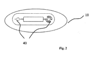
- the segment 10 itself consists of at least one impedance element 20, an insulated support 30 and connection system 40. Said connection system serves for mechanical purpose and for conductive segments interconnection.
- connection system allows to:
- the impedance 20 can be placed on one side, both sides or alternately on one and the other side of the insulation support 30. Except of space benefit the said device has following advantages:
- connection system 40 consists of special connection features provided on insulating support 30.
- Such connection system 40 has basically two ends. At both ends of insulating support 30, the connection system has a hole 75 and 71, through which the segments are fixed to each other. Fixation could be made by rivet or screw, which passes through the hole 75 of one segment and hole 71 of another segment, or by other connection means. By tightening two segments e.g. by the screw, one can fix the angle 50 between mentioned segments 10 and thus set required height and width 60 of the final assembly.
- impedance elements 20 are located under set angle 50 which is smaller then 180°. This arrangement will also result in longer creepage distance of the functional parts comparing to the standard solution used in Fig. 1 , which can give bigger dielectric behavior.
- Insulating support 30 has in addition two small holes 76 and 77.
- the output wire 21 from impedance element 20 passes through one of these holes, depending on size and configuration of selected impedance element 20.
- Oval opening 70 allows soldering of resistive element 20 in a place that is the most suitable for set angle 50.
- conductive element 79 could be used instead of conductive element 78 and/or hole 76 could be used instead of hole 77 on the other side of insulating support 30.
- connection system 40 allows to place impedance
- connection with gap can be used in case the impedance elements are not too long. In such a case all impedances could be placed on the same side of all segments as there is no space constraint. Alternating sides placement could be applied as well, in order to get e.g. better power dissipation from impedance elements used.
- crossed connection according to Fig. 5b can be preferably used.
- alternating side placement might be the only possible placement of impedance elements 20 in order to have the smallest width of final assembly.
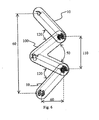
- Fig. 6 shows only example of two segments forming fixed configuration, but there could be also 3 segments in "Z" configuration, etc., with possibility to have more and more branches of the final configuration) forming a single body/support which does not need and does not have the possibility to be adjusted.
- Such fixed support if produced as standard part, can be further height reduced by breaking or cutting off the unused part of said support.
- impedance elements In order to reach required value if impedances required for voltage divider, impedance elements could be assembled to the segments 10 and these segments connected in series, thus increasing total impedance of the divider. In order to decrease production costs or to improve power withstand, it can be advantageous to use standard, and thus cheaper, impedance elements which are connected within given segment in parallel and/or in series, providing required impedance value.
- Preferred solution of impedance divider is using resistive elements, but it can use also capacitive elements or even combination of both.
Landscapes
- Physics & Mathematics (AREA)
- General Physics & Mathematics (AREA)
- Engineering & Computer Science (AREA)
- Power Engineering (AREA)
- Measuring Instrument Details And Bridges, And Automatic Balancing Devices (AREA)
- Measurement Of Current Or Voltage (AREA)
Abstract
Description
- The invention relates to a voltage sensor device, with at least one high voltage segment, and at least one low voltage impedance element, according to the preamble of
claim 1. - Known voltage divider for voltage sensor devices have sensing elements based on voltage divider, which generally consist of the high voltage impedance, e.g. a resistor part and a low voltage impedance part. According to the required application parameters, that means voltage and ratio, the sensing element can be bulky and thus not fitting the insulating sensor body available.
- Furthermore heat dissipated from used impedance elements during operation are flowing upwards, heating up other parts of impedance elements that may limit parameters under which the divider is operating. This is a great disadvantage.
- So it is the object of the invention, to enhance the power dissipation due to impedancies spread inside of the device body.
- So the invention is, the sensing element is adaptive and/or extendable in that way, that at least one high voltage segment, and at least one low voltage impedance element are arranged on an elongated insulating support (30) with adaptive complementary mechanical and electrical interconnection elements (71-79) at least one end of the support element, in order to interconnect at least two such support elements together in a pivotable way.
- In an advantageous embodiment the sensor device can be dimensionaly adapted by the aforesaid adaptive mechancial and electrical interconnection system and/or pivoted by an angle among the segments or supports.
- A further advantageous feature is, that the segmentation and placement of impedance elements allows an relative position under an angle which is smaller that 180°C.
- In a further advantageous embodiment, the resulting value of impedance of the impendance elements can be built up together from standard impedance elements values.
- Furthermore, the impedance elements can either be resistive elements or capacitive elements or combination of both.
- In a further advantageous embodiment, the impedance elements are connected within given segment in parallel and/or in series, providing required impedance value.
- Furthermore, the elements are assembled into at least partly fixed configuration with at least partly given dimensions and at least partly fixed angle between elements, having main fixed insulating support consisting of several elements and/or further possible connection to other separate elements.
- A last advantageous embodiment ist, that the fixed insulating support has a possibility to mechanically reduce the number of elements by breaking or cutting off the unused part of said support.
- An embodiment of the invention is shown in
Figures 1 to 6 . - This invention describes adaptive voltage sensing element assembled from
segments 10. The said voltage sensing element generally consists of high voltage part and low voltage part, corresponding toFig. 1 . The high voltage part consists of at least onesegment 10. Such segment is further called high voltage segment. The low voltage part can be placed on a separate segment (further called low voltage segment) or it can be located on one of the high voltage segments. Thesegment 10 itself consists of at least oneimpedance element 20, aninsulated support 30 andconnection system 40. Said connection system serves for mechanical purpose and for conductive segments interconnection. - Said connection system allows to:
- change
angle 50 between thesegments 10, - change position of the resistive elements
- Above mentioned construction allows adaptation of
dimensions 60 of voltage sensing element. - The
impedance 20 can be placed on one side, both sides or alternately on one and the other side of theinsulation support 30. Except of space benefit the said device has following advantages: - better power dissipation due to impedances spread inside of the
device body 3, - better power dissipation due to impedances placement on both sides of the
insulating support 30, - longer creepage distance of the functional parts,
- resulting value of impedance can assembled from standard values (rows) thus decrease final costs.
-
Insulating support 30 is shown inFig. 3 . Itsconnection system 40 consists of special connection features provided oninsulating support 30.Such connection system 40 has basically two ends. At both ends ofinsulating support 30, the connection system has ahole hole 75 of one segment andhole 71 of another segment, or by other connection means. By tightening two segments e.g. by the screw, one can fix theangle 50 between mentionedsegments 10 and thus set required height andwidth 60 of the final assembly. In order to achieve better power dissipation fromimpedance elements 20, it is preferrable thatimpedance elements 20 are located underset angle 50 which is smaller then 180°. This arrangement will also result in longer creepage distance of the functional parts comparing to the standard solution used inFig. 1 , which can give bigger dielectric behavior. -
Insulating support 30 has in addition twosmall holes output wire 21 fromimpedance element 20 passes through one of these holes, depending on size and configuration ofselected impedance element 20. On the other side ofinsulating support 30 there are twoconductive elements hole holes oval opening impedance elements 20 on different segments. Incase hole 72 is used for soldering of one end of impedance element on theconductive element 78 of theinsulating support 30, one end of impedance element from the other segment has to be connected to the sameconductive element 78, but soldered through theoval opening 70 in order to provide necessary electrical interconnection.Oval opening 70 allows soldering ofresistive element 20 in a place that is the most suitable forset angle 50. - In case
longer impedance element 20 has to be used,conductive element 79 could be used instead ofconductive element 78 and/orhole 76 could be used instead ofhole 77 on the other side ofinsulating support 30. - In addition, the
connection system 40 allows to place impedance - a) with a gap, as shown in
Fig. 5a ; - b) crossed, like shown in
Fig. 5b . - Connection with gap can be used in case the impedance elements are not too long. In such a case all impedances could be placed on the same side of all segments as there is no space constraint. Alternating sides placement could be applied as well, in order to get e.g. better power dissipation from impedance elements used.
- In case of long impedance, crossed connection according to
Fig. 5b can be preferably used. For this configuration, alternating side placement might be the only possible placement ofimpedance elements 20 in order to have the smallest width of final assembly. - It is also possible to have fixed or partly fixed, like shown in
Fig. 6 configuration of such elements for a given application. - a) Partly fixed configuration is characterized in that it consists of
fixed element 100 which contains at least oneimpedance element 20, and at least oneflexible segment 10.Dimensions 60 andangle 120 are still adaptable, but theangle 50 on fixed element is fixed. - b) Fixed configuration contains only
fixed element 110 with at least oneimpedance element 20.Dimensions 60 andangle 50 are fixed. In that case theinsulating support 30 consists of several segment supports; -
Fig. 6 shows only example of two segments forming fixed configuration, but there could be also 3 segments in "Z" configuration, etc., with possibility to have more and more branches of the final configuration) forming a single body/support which does not need and does not have the possibility to be adjusted. Such fixed support, if produced as standard part, can be further height reduced by breaking or cutting off the unused part of said support. - In order to reach required value if impedances required for voltage divider, impedance elements could be assembled to the
segments 10 and these segments connected in series, thus increasing total impedance of the divider. In order to decrease production costs or to improve power withstand, it can be advantageous to use standard, and thus cheaper, impedance elements which are connected within given segment in parallel and/or in series, providing required impedance value. - Preferred solution of impedance divider is using resistive elements, but it can use also capacitive elements or even combination of both.
-
- 1 High voltage impedance; resistor part
- 2 Low voltage impedance
- 3 Insulating sensor body
- 10 Segment
- 20 impedance element, resistive element
- 21 connector
- 30 insulating support
- 40 connection system
- 50 change angle
- 60 dimensions
- 71 hole
- 72 hole
- 73 oval opening
- 74 hole
- 75 hole
- 76 hole
- 77 hole
- 78 conductive element
- 79 conductive element
- 100 fixed element
- 110 fixed element
- 120 angle
Claims (8)
- Voltage sensor device, with at least one high voltage segment, and at least one low voltage impedance element,
characterized in that,
the sensing element is adaptive and/or extendable in that way, that at least one high voltage segment, and at least one low voltage impedance element are arranged on an elongated insulating support (30) with adaptive complementary mechanical and electrical interconnection elements (71-79) at least one end of the support element, in order to interconnect at least two such support elements together in a pivotable way. - Voltage sensor device according to claim 1,
characterized in that,
the sensor device can be dimensionaly adapted by the aforesaid adaptive mechancial and electrical interconnection system and/or pivoted by an angle among the segments or supports (30). - Voltage sensor device according to claim 1,
characterized in that,
the segmentation and placement of impedance elements allows an relative position under an angle which is smaller that 180°C. - Voltage sensor device according to claim 1,
characterized in that,
the resulting value of impedance of the impendance elements can be built up together from standard impedance elements values. - Voltage sensor device according to claim 1,
characterized in that,
the impedance elements are either resistive elements or capacitive elements or combination of both. - Voltage sensor device according to claim 1,
characterized in that,
the impedance elements are connected within given segment in parallel and/or in series, providing required impedance value. - Voltage sensor device according to claim 1,
characterized in that,
the elements are assembled into at least partly fixed configuration with at least partly given dimensions and at least partly fixed angle between elements, having main fixed insulating support consisting of several elements and/or further possible connection to other separate elements. - Voltage sensor device according to claim 1,
characterized in that,
the fixed insulating support has a possibility to mechanically reduce the number of elements by breaking or cutting off the unused part of said support.
Priority Applications (5)
| Application Number | Priority Date | Filing Date | Title |
|---|---|---|---|
| EP13003868.0A EP2833154B1 (en) | 2013-08-02 | 2013-08-02 | Voltage sensor device |
| ARP140102787A AR097077A1 (en) | 2013-08-02 | 2014-07-25 | VOLTAGE SENSOR DEVICE |
| BR102014018821A BR102014018821A8 (en) | 2013-08-02 | 2014-07-30 | VOLTAGE DETECTION DEVICE |
| CN201410470258.8A CN104345205B (en) | 2013-08-02 | 2014-08-01 | Voltage sensing device |
| US14/450,351 US9797930B2 (en) | 2013-08-02 | 2014-08-04 | Voltage sensor device |
Applications Claiming Priority (1)
| Application Number | Priority Date | Filing Date | Title |
|---|---|---|---|
| EP13003868.0A EP2833154B1 (en) | 2013-08-02 | 2013-08-02 | Voltage sensor device |
Publications (2)
| Publication Number | Publication Date |
|---|---|
| EP2833154A1 true EP2833154A1 (en) | 2015-02-04 |
| EP2833154B1 EP2833154B1 (en) | 2022-04-06 |
Family
ID=48915818
Family Applications (1)
| Application Number | Title | Priority Date | Filing Date |
|---|---|---|---|
| EP13003868.0A Active EP2833154B1 (en) | 2013-08-02 | 2013-08-02 | Voltage sensor device |
Country Status (5)
| Country | Link |
|---|---|
| US (1) | US9797930B2 (en) |
| EP (1) | EP2833154B1 (en) |
| CN (1) | CN104345205B (en) |
| AR (1) | AR097077A1 (en) |
| BR (1) | BR102014018821A8 (en) |
Cited By (1)
| Publication number | Priority date | Publication date | Assignee | Title |
|---|---|---|---|---|
| EP3570047A1 (en) * | 2018-05-15 | 2019-11-20 | 3M Innovative Properties Company | Module and system for building a voltage divider for sensing a voltage |
Citations (5)
| Publication number | Priority date | Publication date | Assignee | Title |
|---|---|---|---|---|
| US1047742A (en) * | 1912-03-18 | 1912-12-17 | Frank Buchanan | Electrical resistance. |
| DE606438C (en) * | 1934-12-05 | Metallgesellschaft Ag | High voltage measuring instrument for alternating or direct voltages | |
| WO1999014604A1 (en) * | 1997-09-16 | 1999-03-25 | Trench Switzerland Ag | Voltage divider |
| DE10024335A1 (en) * | 1999-05-17 | 2000-11-23 | Abb Transmit Oy Vaasa | Resistive potential divider for measuring voltage in Medium and High voltage systems accommodated in bushing insulator and wound around live conductor |
| US20060012382A1 (en) * | 2004-07-19 | 2006-01-19 | Fieldmetrics Inc | Modular voltage sensor |
Family Cites Families (4)
| Publication number | Priority date | Publication date | Assignee | Title |
|---|---|---|---|---|
| AU2005204695C1 (en) * | 2004-01-07 | 2010-03-04 | Suparules Limited | Voltage measuring device |
| CN201163287Y (en) * | 2007-08-01 | 2008-12-10 | 大连新大路电气传动技术有限责任公司 | High voltage type voltage transducer with supporting insulator function |
| EP2605023B1 (en) * | 2011-12-16 | 2017-07-26 | Arteche Lantegi Elkartea, S.A. | High-voltage voltage divider and connector comprising said divider |
| FR3003354B1 (en) * | 2013-03-12 | 2015-04-17 | Alstom Technology Ltd | RESISTIVE ELEMENT, RC MODULE AND RC VOLTAGE DIVIDER FOR HIGH VOLTAGE ELECTRICAL STATION INSULATED BY A DIELECTRIC FLUID |
-
2013
- 2013-08-02 EP EP13003868.0A patent/EP2833154B1/en active Active
-
2014
- 2014-07-25 AR ARP140102787A patent/AR097077A1/en unknown
- 2014-07-30 BR BR102014018821A patent/BR102014018821A8/en not_active Application Discontinuation
- 2014-08-01 CN CN201410470258.8A patent/CN104345205B/en active Active
- 2014-08-04 US US14/450,351 patent/US9797930B2/en active Active
Patent Citations (5)
| Publication number | Priority date | Publication date | Assignee | Title |
|---|---|---|---|---|
| DE606438C (en) * | 1934-12-05 | Metallgesellschaft Ag | High voltage measuring instrument for alternating or direct voltages | |
| US1047742A (en) * | 1912-03-18 | 1912-12-17 | Frank Buchanan | Electrical resistance. |
| WO1999014604A1 (en) * | 1997-09-16 | 1999-03-25 | Trench Switzerland Ag | Voltage divider |
| DE10024335A1 (en) * | 1999-05-17 | 2000-11-23 | Abb Transmit Oy Vaasa | Resistive potential divider for measuring voltage in Medium and High voltage systems accommodated in bushing insulator and wound around live conductor |
| US20060012382A1 (en) * | 2004-07-19 | 2006-01-19 | Fieldmetrics Inc | Modular voltage sensor |
Cited By (2)
| Publication number | Priority date | Publication date | Assignee | Title |
|---|---|---|---|---|
| EP3570047A1 (en) * | 2018-05-15 | 2019-11-20 | 3M Innovative Properties Company | Module and system for building a voltage divider for sensing a voltage |
| WO2019220371A1 (en) * | 2018-05-15 | 2019-11-21 | 3M Innovative Properties Company | Module and system for building a voltage divider for sensing a voltage |
Also Published As
| Publication number | Publication date |
|---|---|
| BR102014018821A2 (en) | 2015-09-29 |
| CN104345205A (en) | 2015-02-11 |
| AR097077A1 (en) | 2016-02-17 |
| US20150035553A1 (en) | 2015-02-05 |
| CN104345205B (en) | 2018-11-20 |
| BR102014018821A8 (en) | 2017-12-19 |
| EP2833154B1 (en) | 2022-04-06 |
| US9797930B2 (en) | 2017-10-24 |
Similar Documents
| Publication | Publication Date | Title |
|---|---|---|
| EP2772204A3 (en) | Articulatable surgical instruments with conductive pathways for signal communication | |
| MX2015011327A (en) | Articulatable surgical instruments with conductive pathways for signal communication. | |
| EP2375510A1 (en) | Over-temperature over-current protection power plug | |
| EP2053706A3 (en) | Electric motor commutator | |
| ATE488888T1 (en) | ELECTRICAL CONNECTOR | |
| RU2016107879A (en) | COOLING DEVICE FOR ELECTRICAL OR ELECTRONIC DEVICE AND ELECTRIC OR ELECTRONIC DEVICE, IN PARTICULAR AUTOMATIC CIRCUIT BREAKER CONTAINING SUCH COOLING DEVICE | |
| JP2016119353A (en) | Thermistor | |
| BR102014032286B1 (en) | BUS ADAPTER AND BUS SYSTEM AND A BUS ADAPTER | |
| RU2016108109A (en) | HYDRAULIC VALVE | |
| WO2018091654A3 (en) | Implantable electric multi-pole connection structure | |
| US20170303341A1 (en) | Heating rod | |
| EP2833154A1 (en) | Voltage sensor device | |
| FR3050066B1 (en) | ELECTRIC CABLE WITH IMPROVED GALVANIC CORROSION RESISTANCE | |
| RU2016123938A (en) | LIGHTING DEVICE | |
| EP2765840A3 (en) | Switching assembly | |
| CN107078417B (en) | Junction Box | |
| EP1777645A3 (en) | Semiconductor device | |
| JP4550114B2 (en) | High performance load resistor | |
| EP2991110B1 (en) | Circuit protection device | |
| EP3979269A4 (en) | Insulated electrical wire, coil, and electrical and electronic instrument | |
| IN2014DE02350A (en) | ||
| KR102546013B1 (en) | Device for limiting leakage current of power electric transmission line | |
| AU2012200788A1 (en) | Card incorporating a transponder | |
| DE102012212951B4 (en) | Roof control unit of a vehicle interior lighting | |
| US9538678B2 (en) | Voltage controller for an electric cooling fan |
Legal Events
| Date | Code | Title | Description |
|---|---|---|---|
| 17P | Request for examination filed |
Effective date: 20130802 |
|
| AK | Designated contracting states |
Kind code of ref document: A1 Designated state(s): AL AT BE BG CH CY CZ DE DK EE ES FI FR GB GR HR HU IE IS IT LI LT LU LV MC MK MT NL NO PL PT RO RS SE SI SK SM TR |
|
| AX | Request for extension of the european patent |
Extension state: BA ME |
|
| PUAI | Public reference made under article 153(3) epc to a published international application that has entered the european phase |
Free format text: ORIGINAL CODE: 0009012 |
|
| R17P | Request for examination filed (corrected) |
Effective date: 20150803 |
|
| RBV | Designated contracting states (corrected) |
Designated state(s): AL AT BE BG CH CY CZ DE DK EE ES FI FR GB GR HR HU IE IS IT LI LT LU LV MC MK MT NL NO PL PT RO RS SE SI SK SM TR |
|
| 17Q | First examination report despatched |
Effective date: 20150909 |
|
| RAP1 | Party data changed (applicant data changed or rights of an application transferred) |
Owner name: ABB SCHWEIZ AG |
|
| STAA | Information on the status of an ep patent application or granted ep patent |
Free format text: STATUS: EXAMINATION IS IN PROGRESS |
|
| GRAP | Despatch of communication of intention to grant a patent |
Free format text: ORIGINAL CODE: EPIDOSNIGR1 |
|
| STAA | Information on the status of an ep patent application or granted ep patent |
Free format text: STATUS: GRANT OF PATENT IS INTENDED |
|
| INTG | Intention to grant announced |
Effective date: 20211119 |
|
| GRAS | Grant fee paid |
Free format text: ORIGINAL CODE: EPIDOSNIGR3 |
|
| GRAA | (expected) grant |
Free format text: ORIGINAL CODE: 0009210 |
|
| STAA | Information on the status of an ep patent application or granted ep patent |
Free format text: STATUS: THE PATENT HAS BEEN GRANTED |
|
| RIN1 | Information on inventor provided before grant (corrected) |
Inventor name: PAVLAS, MAREK Inventor name: PODZEMNY, JAROMIR Inventor name: JAVORA, RADEK Inventor name: HRABCIK, MIROSLAV |
|
| AK | Designated contracting states |
Kind code of ref document: B1 Designated state(s): AL AT BE BG CH CY CZ DE DK EE ES FI FR GB GR HR HU IE IS IT LI LT LU LV MC MK MT NL NO PL PT RO RS SE SI SK SM TR |
|
| RAP3 | Party data changed (applicant data changed or rights of an application transferred) |
Owner name: ABB SCHWEIZ AG |
|
| REG | Reference to a national code |
Ref country code: GB Ref legal event code: FG4D |
|
| REG | Reference to a national code |
Ref country code: CH Ref legal event code: EP |
|
| REG | Reference to a national code |
Ref country code: AT Ref legal event code: REF Ref document number: 1481829 Country of ref document: AT Kind code of ref document: T Effective date: 20220415 |
|
| REG | Reference to a national code |
Ref country code: DE Ref legal event code: R096 Ref document number: 602013081303 Country of ref document: DE |
|
| REG | Reference to a national code |
Ref country code: IE Ref legal event code: FG4D |
|
| REG | Reference to a national code |
Ref country code: LT Ref legal event code: MG9D |
|
| REG | Reference to a national code |
Ref country code: NL Ref legal event code: MP Effective date: 20220406 |
|
| PG25 | Lapsed in a contracting state [announced via postgrant information from national office to epo] |
Ref country code: NL Free format text: LAPSE BECAUSE OF FAILURE TO SUBMIT A TRANSLATION OF THE DESCRIPTION OR TO PAY THE FEE WITHIN THE PRESCRIBED TIME-LIMIT Effective date: 20220406 |
|
| PG25 | Lapsed in a contracting state [announced via postgrant information from national office to epo] |
Ref country code: SE Free format text: LAPSE BECAUSE OF FAILURE TO SUBMIT A TRANSLATION OF THE DESCRIPTION OR TO PAY THE FEE WITHIN THE PRESCRIBED TIME-LIMIT Effective date: 20220406 Ref country code: PT Free format text: LAPSE BECAUSE OF FAILURE TO SUBMIT A TRANSLATION OF THE DESCRIPTION OR TO PAY THE FEE WITHIN THE PRESCRIBED TIME-LIMIT Effective date: 20220808 Ref country code: NO Free format text: LAPSE BECAUSE OF FAILURE TO SUBMIT A TRANSLATION OF THE DESCRIPTION OR TO PAY THE FEE WITHIN THE PRESCRIBED TIME-LIMIT Effective date: 20220706 Ref country code: LT Free format text: LAPSE BECAUSE OF FAILURE TO SUBMIT A TRANSLATION OF THE DESCRIPTION OR TO PAY THE FEE WITHIN THE PRESCRIBED TIME-LIMIT Effective date: 20220406 Ref country code: HR Free format text: LAPSE BECAUSE OF FAILURE TO SUBMIT A TRANSLATION OF THE DESCRIPTION OR TO PAY THE FEE WITHIN THE PRESCRIBED TIME-LIMIT Effective date: 20220406 Ref country code: GR Free format text: LAPSE BECAUSE OF FAILURE TO SUBMIT A TRANSLATION OF THE DESCRIPTION OR TO PAY THE FEE WITHIN THE PRESCRIBED TIME-LIMIT Effective date: 20220707 Ref country code: FI Free format text: LAPSE BECAUSE OF FAILURE TO SUBMIT A TRANSLATION OF THE DESCRIPTION OR TO PAY THE FEE WITHIN THE PRESCRIBED TIME-LIMIT Effective date: 20220406 Ref country code: ES Free format text: LAPSE BECAUSE OF FAILURE TO SUBMIT A TRANSLATION OF THE DESCRIPTION OR TO PAY THE FEE WITHIN THE PRESCRIBED TIME-LIMIT Effective date: 20220406 Ref country code: BG Free format text: LAPSE BECAUSE OF FAILURE TO SUBMIT A TRANSLATION OF THE DESCRIPTION OR TO PAY THE FEE WITHIN THE PRESCRIBED TIME-LIMIT Effective date: 20220706 |
|
| PG25 | Lapsed in a contracting state [announced via postgrant information from national office to epo] |
Ref country code: RS Free format text: LAPSE BECAUSE OF FAILURE TO SUBMIT A TRANSLATION OF THE DESCRIPTION OR TO PAY THE FEE WITHIN THE PRESCRIBED TIME-LIMIT Effective date: 20220406 Ref country code: PL Free format text: LAPSE BECAUSE OF FAILURE TO SUBMIT A TRANSLATION OF THE DESCRIPTION OR TO PAY THE FEE WITHIN THE PRESCRIBED TIME-LIMIT Effective date: 20220406 Ref country code: LV Free format text: LAPSE BECAUSE OF FAILURE TO SUBMIT A TRANSLATION OF THE DESCRIPTION OR TO PAY THE FEE WITHIN THE PRESCRIBED TIME-LIMIT Effective date: 20220406 Ref country code: IS Free format text: LAPSE BECAUSE OF FAILURE TO SUBMIT A TRANSLATION OF THE DESCRIPTION OR TO PAY THE FEE WITHIN THE PRESCRIBED TIME-LIMIT Effective date: 20220806 |
|
| REG | Reference to a national code |
Ref country code: DE Ref legal event code: R097 Ref document number: 602013081303 Country of ref document: DE |
|
| PG25 | Lapsed in a contracting state [announced via postgrant information from national office to epo] |
Ref country code: SM Free format text: LAPSE BECAUSE OF FAILURE TO SUBMIT A TRANSLATION OF THE DESCRIPTION OR TO PAY THE FEE WITHIN THE PRESCRIBED TIME-LIMIT Effective date: 20220406 Ref country code: SK Free format text: LAPSE BECAUSE OF FAILURE TO SUBMIT A TRANSLATION OF THE DESCRIPTION OR TO PAY THE FEE WITHIN THE PRESCRIBED TIME-LIMIT Effective date: 20220406 Ref country code: RO Free format text: LAPSE BECAUSE OF FAILURE TO SUBMIT A TRANSLATION OF THE DESCRIPTION OR TO PAY THE FEE WITHIN THE PRESCRIBED TIME-LIMIT Effective date: 20220406 Ref country code: EE Free format text: LAPSE BECAUSE OF FAILURE TO SUBMIT A TRANSLATION OF THE DESCRIPTION OR TO PAY THE FEE WITHIN THE PRESCRIBED TIME-LIMIT Effective date: 20220406 Ref country code: DK Free format text: LAPSE BECAUSE OF FAILURE TO SUBMIT A TRANSLATION OF THE DESCRIPTION OR TO PAY THE FEE WITHIN THE PRESCRIBED TIME-LIMIT Effective date: 20220406 Ref country code: CZ Free format text: LAPSE BECAUSE OF FAILURE TO SUBMIT A TRANSLATION OF THE DESCRIPTION OR TO PAY THE FEE WITHIN THE PRESCRIBED TIME-LIMIT Effective date: 20220406 |
|
| PLBE | No opposition filed within time limit |
Free format text: ORIGINAL CODE: 0009261 |
|
| STAA | Information on the status of an ep patent application or granted ep patent |
Free format text: STATUS: NO OPPOSITION FILED WITHIN TIME LIMIT |
|
| 26N | No opposition filed |
Effective date: 20230110 |
|
| PG25 | Lapsed in a contracting state [announced via postgrant information from national office to epo] |
Ref country code: MC Free format text: LAPSE BECAUSE OF FAILURE TO SUBMIT A TRANSLATION OF THE DESCRIPTION OR TO PAY THE FEE WITHIN THE PRESCRIBED TIME-LIMIT Effective date: 20220406 Ref country code: AL Free format text: LAPSE BECAUSE OF FAILURE TO SUBMIT A TRANSLATION OF THE DESCRIPTION OR TO PAY THE FEE WITHIN THE PRESCRIBED TIME-LIMIT Effective date: 20220406 |
|
| REG | Reference to a national code |
Ref country code: CH Ref legal event code: PL |
|
| GBPC | Gb: european patent ceased through non-payment of renewal fee |
Effective date: 20220802 |
|
| PG25 | Lapsed in a contracting state [announced via postgrant information from national office to epo] |
Ref country code: LU Free format text: LAPSE BECAUSE OF NON-PAYMENT OF DUE FEES Effective date: 20220802 Ref country code: LI Free format text: LAPSE BECAUSE OF NON-PAYMENT OF DUE FEES Effective date: 20220831 Ref country code: CH Free format text: LAPSE BECAUSE OF NON-PAYMENT OF DUE FEES Effective date: 20220831 |
|
| REG | Reference to a national code |
Ref country code: BE Ref legal event code: MM Effective date: 20220831 |
|
| PG25 | Lapsed in a contracting state [announced via postgrant information from national office to epo] |
Ref country code: SI Free format text: LAPSE BECAUSE OF FAILURE TO SUBMIT A TRANSLATION OF THE DESCRIPTION OR TO PAY THE FEE WITHIN THE PRESCRIBED TIME-LIMIT Effective date: 20220406 |
|
| REG | Reference to a national code |
Ref country code: AT Ref legal event code: UEP Ref document number: 1481829 Country of ref document: AT Kind code of ref document: T Effective date: 20220406 |
|
| PG25 | Lapsed in a contracting state [announced via postgrant information from national office to epo] |
Ref country code: IE Free format text: LAPSE BECAUSE OF NON-PAYMENT OF DUE FEES Effective date: 20220802 |
|
| PG25 | Lapsed in a contracting state [announced via postgrant information from national office to epo] |
Ref country code: BE Free format text: LAPSE BECAUSE OF NON-PAYMENT OF DUE FEES Effective date: 20220831 |
|
| PG25 | Lapsed in a contracting state [announced via postgrant information from national office to epo] |
Ref country code: GB Free format text: LAPSE BECAUSE OF NON-PAYMENT OF DUE FEES Effective date: 20220802 |
|
| PG25 | Lapsed in a contracting state [announced via postgrant information from national office to epo] |
Ref country code: HU Free format text: LAPSE BECAUSE OF FAILURE TO SUBMIT A TRANSLATION OF THE DESCRIPTION OR TO PAY THE FEE WITHIN THE PRESCRIBED TIME-LIMIT; INVALID AB INITIO Effective date: 20130802 |
|
| PG25 | Lapsed in a contracting state [announced via postgrant information from national office to epo] |
Ref country code: MK Free format text: LAPSE BECAUSE OF FAILURE TO SUBMIT A TRANSLATION OF THE DESCRIPTION OR TO PAY THE FEE WITHIN THE PRESCRIBED TIME-LIMIT Effective date: 20220406 Ref country code: CY Free format text: LAPSE BECAUSE OF FAILURE TO SUBMIT A TRANSLATION OF THE DESCRIPTION OR TO PAY THE FEE WITHIN THE PRESCRIBED TIME-LIMIT Effective date: 20220406 |
|
| PG25 | Lapsed in a contracting state [announced via postgrant information from national office to epo] |
Ref country code: TR Free format text: LAPSE BECAUSE OF FAILURE TO SUBMIT A TRANSLATION OF THE DESCRIPTION OR TO PAY THE FEE WITHIN THE PRESCRIBED TIME-LIMIT Effective date: 20220406 |
|
| PG25 | Lapsed in a contracting state [announced via postgrant information from national office to epo] |
Ref country code: MT Free format text: LAPSE BECAUSE OF FAILURE TO SUBMIT A TRANSLATION OF THE DESCRIPTION OR TO PAY THE FEE WITHIN THE PRESCRIBED TIME-LIMIT Effective date: 20220406 |
|
| PG25 | Lapsed in a contracting state [announced via postgrant information from national office to epo] |
Ref country code: BG Free format text: LAPSE BECAUSE OF FAILURE TO SUBMIT A TRANSLATION OF THE DESCRIPTION OR TO PAY THE FEE WITHIN THE PRESCRIBED TIME-LIMIT Effective date: 20220406 |
|
| PG25 | Lapsed in a contracting state [announced via postgrant information from national office to epo] |
Ref country code: BG Free format text: LAPSE BECAUSE OF FAILURE TO SUBMIT A TRANSLATION OF THE DESCRIPTION OR TO PAY THE FEE WITHIN THE PRESCRIBED TIME-LIMIT Effective date: 20220406 |
|
| PGFP | Annual fee paid to national office [announced via postgrant information from national office to epo] |
Ref country code: DE Payment date: 20250820 Year of fee payment: 13 |
|
| PGFP | Annual fee paid to national office [announced via postgrant information from national office to epo] |
Ref country code: IT Payment date: 20250825 Year of fee payment: 13 |
|
| PGFP | Annual fee paid to national office [announced via postgrant information from national office to epo] |
Ref country code: FR Payment date: 20250829 Year of fee payment: 13 Ref country code: AT Payment date: 20250821 Year of fee payment: 13 |