EP2830257B1 - Atca backplane - Google Patents
Atca backplane Download PDFInfo
- Publication number
- EP2830257B1 EP2830257B1 EP13791669.8A EP13791669A EP2830257B1 EP 2830257 B1 EP2830257 B1 EP 2830257B1 EP 13791669 A EP13791669 A EP 13791669A EP 2830257 B1 EP2830257 B1 EP 2830257B1
- Authority
- EP
- European Patent Office
- Prior art keywords
- backplane
- board
- atca
- slots
- area
- Prior art date
- Legal status (The legal status is an assumption and is not a legal conclusion. Google has not performed a legal analysis and makes no representation as to the accuracy of the status listed.)
- Active
Links
Images
Classifications
-
- H—ELECTRICITY
- H04—ELECTRIC COMMUNICATION TECHNIQUE
- H04L—TRANSMISSION OF DIGITAL INFORMATION, e.g. TELEGRAPHIC COMMUNICATION
- H04L12/00—Data switching networks
- H04L12/64—Hybrid switching systems
- H04L12/6418—Hybrid transport
-
- G—PHYSICS
- G06—COMPUTING OR CALCULATING; COUNTING
- G06F—ELECTRIC DIGITAL DATA PROCESSING
- G06F1/00—Details not covered by groups G06F3/00 - G06F13/00 and G06F21/00
- G06F1/16—Constructional details or arrangements
- G06F1/18—Packaging or power distribution
- G06F1/183—Internal mounting support structures, e.g. for supporting printed circuit boards
- G06F1/185—Mounting of expansion boards
- G06F1/186—Securing of expansion boards in correspondence to slots provided at the computer enclosure
-
- H—ELECTRICITY
- H04—ELECTRIC COMMUNICATION TECHNIQUE
- H04L—TRANSMISSION OF DIGITAL INFORMATION, e.g. TELEGRAPHIC COMMUNICATION
- H04L12/00—Data switching networks
- H04L12/66—Arrangements for connecting between networks having differing types of switching systems, e.g. gateways
-
- H—ELECTRICITY
- H04—ELECTRIC COMMUNICATION TECHNIQUE
- H04Q—SELECTING
- H04Q2213/00—Indexing scheme relating to selecting arrangements in general and for multiplex systems
- H04Q2213/13003—Constructional details of switching devices
-
- H—ELECTRICITY
- H04—ELECTRIC COMMUNICATION TECHNIQUE
- H04Q—SELECTING
- H04Q2213/00—Indexing scheme relating to selecting arrangements in general and for multiplex systems
- H04Q2213/13076—Distributing frame, MDF, cross-connect switch
Definitions
- the disclosure relates to computer technology, and in particular to an ATCA (Advanced Telecom Computing Architecture) backplane.
- ATCA Advanced Telecom Computing Architecture
- ATCA plays an important role in a next-generation telecom network.
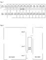
- Fig.1 is a diagram of board distribution of a typical ATCA 14-slot shelf. Boards in the shelf are divided into front boards and rear boards.
- a front board may be a HUB BOARD or a NODE BOARD.
- a rear board is inserted opposite a front board as an interface expansion unit of the front board, and provides an external interface.
- An interface connecting a front board to a backplane is defined in area 1 or area 2 by function.
- An interface such as a power supply interface or a system management interface, is defined in area 1.
- a data transmission channel is defined in area 2.
- Fig.2 is a schematic diagram of a typical connection between a front board and a rear board.
- An interface connecting a front board to a rear board is defined in area 3.
- a front board is connected directly to a rear board via corresponding plugging pieces, without the need of interconnection by a backplane.
- a front board is mainly for service processing. Due to a limited size, a rear board can serve only as an expansion to an interface of a front board and provide some simple interfaces such as a keyboard, mouse, or display interface, but can hardly provide strong service processing capability, thus leading to waste of slot resources on the rear board.
- the first backplane (310) provides a power management interface defined in the first region (Zone 1) of an ATCA standard, an IPMB (Platform Management Bus) interface (102) for a platform management, a base interface (103) for exchanging control information between slots defined in the second region (Zone 2), and a fabric interface (103) for exchanging packet data between slots, among the first and second switch slots and a plurality of node slots.
- Self-managers (205, 206) manage states of boards, which are mounted at the first and second switch slots and the plural node slots, and operations of turning on/off power through the IPMB interface (102) of the first backplane (310).
- the second backplane (320) provides an additional fabric interface (301) among the first and second switch slots and the multiple node slots through the third region (Zone 3) of the ATCA standards.
- a chassis includes a plurality of slots to receive modules.
- the chassis further includes a first backplane to couple to modules that are received in the plurality of slots.
- the modules are to couple to the first backplane via a first communication interface on each module.
- the chassis also includes a second backplane to couple to at least a subset of the modules via a second communication interface on each of the subset of modules.
- One of the backplanes may be located in an upper or lower air plenum and used to interconnect modules slid along the slots from opposite directions.
- Some of the module connectors may be retractable to enable the modules to move into the chassis.
- the interface may be electrical, optical inductive or capacitive.
- a system comprises a primary backplane and a secondary backplane.
- the primary backplane has a surface region substantially devoid of components and a plurality of connectors to which electronic devices can be mated.
- the secondary backplane is removably mated to the primary backplane within the region.
- the secondary backplane has at least two connectors adapted to mate to at least two of the electronic devices. At least two electronic devices communicatively interconnect through the primary and secondary backplanes.
- the invention is related to an ATCA backplane according to claim 1. Further embodiments of the invention are defined by the dependent claims.
- Embodiments of the disclosure provide an ATCA backplane containing a backplane-pair structure to increase a number of available node board slots of an ATCA system and enhance processing capability of the ATCA system.
- the ATCA backplane includes at least one backplane pair of a front backplane and a rear backplane interconnected via a connector. At least one backplane in the ATCA backplane contains a slot for a hub board. Each backplane in the at least one backplane pair contains slots for at least one node board.
- the slot for the hub board in the ATCA backplane includes slots for at least two hub boards.
- a front board and a rear board in the ATCA backplane are no longer inserted into each other directly; and a rear board in the ATCA backplane is not like one defined in a PICMG3.0 specification either.
- a backplane in the ATCA backplane extends to an area 3 on a (front or rear) board to which the backplane is connected, and is provided with a plug connected to a slot for the area 3 on the board.
- a slot for an area 3 on a hub board or a node board connected to a backplane in the ATCA backplane is connected, via backplane wiring, to one or more slots of the front backplane or the rear backplane, the slots being specifically designed for providing an external or internal interface of a shelf.
- architecture of interconnection of a front backplane and a rear backplane based on the PICMG3.0 specification may be used, abandoning original requirement of configuration of a rear board for each front board, such that a board inserted to either a front backplane or a rear backplane may be a node board or a hub board.
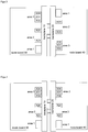
- a backplane 10 is connected to a backplane 20 via a connector; a node board 30 connected to the backplane 10 contains an area 1, an area 2, and an area 3; a node board 40 connected to the backplane 20 contains an area 1, an area 2, and an area 3.
- the node board 40 may be of a type same as or different from the type of the node board 30.
- a slot for the area 2 on an aforementioned node board is as defined in the PICMG3.0 specification.
- a slot for the area 3 on a node board is connected to the plug of a backplane, so as to be connected to one or more slots of a front backplane or a rear backplane via backplane wiring, the slots being specifically designed for providing an external or internal interface of the shelf.
- slots for board insertion on the front backplane are arranged asymmetric to slots for board insertion on the rear backplane.
- arrangement as shown in Fig.4 may also be possible, such that slots for board insertion on the front backplane are symmetric to slots for board insertion on the rear backplane.
- a front backplane and /or a rear backplane in the ATCA backplane according to the disclosure may also be connected to a hub board.
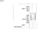
- a slot for the area 2 on a hub board 50 is as defined in the PICMG3.0 specification.
- a slot for the area 3 on the hub board 50 is connected to the plug of a backplane, so as to be connected to one or more slots of a front backplane or a rear backplane via backplane wiring, the slots being specifically designed for providing an external or internal interface of the shelf.
- there may be at least two such hub boards which may be arranged on the same backplane or on two different backplanes respectively. The two hub boards may back up each other.
- An aforementioned ATCA backplane when installed in an ATCA shelf, may back up an existing function module such as a power supply module (PEM), a shelf management module (CMM), a fan module (FCM), a shelf data module (CDM), and the like.
- PEM power supply module
- CCM shelf management module
- FCM fan module
- CDM shelf data module
- a user-defined interface is arranged in area 3 on a board, which ensures a flexible system design.
- a signal in the area 3 on a hub board can be extracted via a specially designed slot, which, plus arrangement of an external interface, ensures capability of shelf cascade;
- a signal in the area 3 on a node board can also be extracted via a specially designed slot, and an external interface remains as well.
- a front backplane and a rear backplane for installing the ATCA backplane may be connected tightly into one piece via a connector and a fastener between the backplanes.
- Logically the front backplane and the rear backplane connected to each other may be taken as a separate backplane with both front and rear faces having slots for board insertion.
- a connector between a front backplane and a rear backplane may convey a signal, electric energy and the like.
- the ATCA backplane herein includes at least a front backplane and a rear backplane interconnected via a connector.
- Each backplane in the ATCA backplane contains slots for at least one node board.
- at least one backplane in the ATCA backplane is arranged with a slot for a hub board. Therefore, a node board may be inserted in either a front backplane or a rear backplane in the ATCA backplane herein, increasing a number of node board slots, expanding slot resources, and enhancing system processing capability.
Landscapes
- Engineering & Computer Science (AREA)
- Computer Networks & Wireless Communication (AREA)
- Signal Processing (AREA)
- Theoretical Computer Science (AREA)
- General Engineering & Computer Science (AREA)
- Computer Hardware Design (AREA)
- Power Engineering (AREA)
- Human Computer Interaction (AREA)
- Physics & Mathematics (AREA)
- General Physics & Mathematics (AREA)
- Mounting Of Printed Circuit Boards And The Like (AREA)
- Data Exchanges In Wide-Area Networks (AREA)
- Use Of Switch Circuits For Exchanges And Methods Of Control Of Multiplex Exchanges (AREA)
- Structure Of Telephone Exchanges (AREA)
Description
- The disclosure relates to computer technology, and in particular to an ATCA (Advanced Telecom Computing Architecture) backplane.
- With development of a telecom service, a telecom operator focuses more on flexibility, openness, scalability and service stability of telecom platform. Therefore, ATCA plays an important role in a next-generation telecom network.
-
Fig.1 is a diagram of board distribution of a typical ATCA 14-slot shelf. Boards in the shelf are divided into front boards and rear boards. A front board may be a HUB BOARD or a NODE BOARD. A rear board is inserted opposite a front board as an interface expansion unit of the front board, and provides an external interface. - An interface connecting a front board to a backplane is defined in
area 1 orarea 2 by function. An interface, such as a power supply interface or a system management interface, is defined inarea 1. A data transmission channel is defined inarea 2.Fig.2 is a schematic diagram of a typical connection between a front board and a rear board. An interface connecting a front board to a rear board is defined inarea 3. A front board is connected directly to a rear board via corresponding plugging pieces, without the need of interconnection by a backplane. - At present, a front board is mainly for service processing. Due to a limited size, a rear board can serve only as an expansion to an interface of a front board and provide some simple interfaces such as a keyboard, mouse, or display interface, but can hardly provide strong service processing capability, thus leading to waste of slot resources on the rear board.
- According to
KR 2007 0061197 A - According to
US 7 458 815 B2 , a chassis includes a plurality of slots to receive modules. The chassis further includes a first backplane to couple to modules that are received in the plurality of slots. The modules are to couple to the first backplane via a first communication interface on each module. The chassis also includes a second backplane to couple to at least a subset of the modules via a second communication interface on each of the subset of modules. One of the backplanes may be located in an upper or lower air plenum and used to interconnect modules slid along the slots from opposite directions. Some of the module connectors may be retractable to enable the modules to move into the chassis. The interface may be electrical, optical inductive or capacitive. - According to
US 7,780,455 B2 , a system comprises a primary backplane and a secondary backplane. The primary backplane has a surface region substantially devoid of components and a plurality of connectors to which electronic devices can be mated. The secondary backplane is removably mated to the primary backplane within the region. The secondary backplane has at least two connectors adapted to mate to at least two of the electronic devices. At least two electronic devices communicatively interconnect through the primary and secondary backplanes. - The invention is related to an ATCA backplane according to
claim 1. Further embodiments of the invention are defined by the dependent claims. -
-
Fig.1 is a diagram of board distribution of a typical 14-slot shelf; -
Fig.2 is a schematic diagram of a typical connection between a front board and a rear board; -
Fig.3 is a schematic diagram of node board connection to a backplane pair according to an embodiment of the disclosure; -
Fig.4 is a schematic diagram of node board connection to a backplane pair according to an embodiment of the disclosure; and -
Fig.5 is a schematic diagram of hub board connection to a backplane pair according to an embodiment of the disclosure. - Embodiments of the disclosure provide an ATCA backplane containing a backplane-pair structure to increase a number of available node board slots of an ATCA system and enhance processing capability of the ATCA system.
- The ATCA backplane includes at least one backplane pair of a front backplane and a rear backplane interconnected via a connector. At least one backplane in the ATCA backplane contains a slot for a hub board. Each backplane in the at least one backplane pair contains slots for at least one node board.
- In general, the slot for the hub board in the ATCA backplane includes slots for at least two hub boards.
- Moreover, a front board and a rear board in the ATCA backplane are no longer inserted into each other directly; and a rear board in the ATCA backplane is not like one defined in a PICMG3.0 specification either. A backplane in the ATCA backplane extends to an
area 3 on a (front or rear) board to which the backplane is connected, and is provided with a plug connected to a slot for thearea 3 on the board. - In addition, a slot for an
area 3 on a hub board or a node board connected to a backplane in the ATCA backplane is connected, via backplane wiring, to one or more slots of the front backplane or the rear backplane, the slots being specifically designed for providing an external or internal interface of a shelf. - In an embodiment, architecture of interconnection of a front backplane and a rear backplane based on the PICMG3.0 specification may be used, abandoning original requirement of configuration of a rear board for each front board, such that a board inserted to either a front backplane or a rear backplane may be a node board or a hub board.
- In
Fig.3 , abackplane 10 is connected to abackplane 20 via a connector; anode board 30 connected to thebackplane 10 contains anarea 1, anarea 2, and anarea 3; anode board 40 connected to thebackplane 20 contains anarea 1, anarea 2, and anarea 3. Thenode board 40 may be of a type same as or different from the type of thenode board 30. - A slot for the
area 2 on an aforementioned node board is as defined in the PICMG3.0 specification. A slot for thearea 3 on a node board is connected to the plug of a backplane, so as to be connected to one or more slots of a front backplane or a rear backplane via backplane wiring, the slots being specifically designed for providing an external or internal interface of the shelf. - In
Fig.3 , slots for board insertion on the front backplane are arranged asymmetric to slots for board insertion on the rear backplane. In fact, arrangement as shown inFig.4 may also be possible, such that slots for board insertion on the front backplane are symmetric to slots for board insertion on the rear backplane. - in an actual application, a front backplane and /or a rear backplane in the ATCA backplane according to the disclosure may also be connected to a hub board. As shown in
Fig.5 , a slot for thearea 2 on ahub board 50 is as defined in the PICMG3.0 specification. A slot for thearea 3 on thehub board 50 is connected to the plug of a backplane, so as to be connected to one or more slots of a front backplane or a rear backplane via backplane wiring, the slots being specifically designed for providing an external or internal interface of the shelf. In general, there may be at least two such hub boards which may be arranged on the same backplane or on two different backplanes respectively. The two hub boards may back up each other. - An aforementioned ATCA backplane, when installed in an ATCA shelf, may back up an existing function module such as a power supply module (PEM), a shelf management module (CMM), a fan module (FCM), a shelf data module (CDM), and the like.
- Note that a user-defined interface is arranged in
area 3 on a board, which ensures a flexible system design. A signal in thearea 3 on a hub board can be extracted via a specially designed slot, which, plus arrangement of an external interface, ensures capability of shelf cascade; A signal in thearea 3 on a node board can also be extracted via a specially designed slot, and an external interface remains as well. - After being manufactured separately, a front backplane and a rear backplane for installing the ATCA backplane may be connected tightly into one piece via a connector and a fastener between the backplanes. Logically the front backplane and the rear backplane connected to each other may be taken as a separate backplane with both front and rear faces having slots for board insertion. In addition, a connector between a front backplane and a rear backplane may convey a signal, electric energy and the like. There may be multiple inter-backplane connectors, and the inter-backplane connectors may be of one or more types.
- It may be seen from the description that an ATCA backplane herein applies to a scenario as follow.
- 1) In an existing ATCA system, respective interfaces for a keyboard, a mouse, and a display are provided independently by a rear board for a node board. In actual use, it's impossible to configure a keyboard, a mouse, and a display for each rear board. Instead, an external switch for keyboard, mouse, and display sharing is arranged, which not only occupies shelf space, but also requires much wiring. With the ATCA backplane herein, a node board no longer requires a rear board. A keyboard, mouse, or display signal of
area 3 on any node board may gather directly to a specially designed slot on a backplane. A board connected to the specially designed slot then serves as a switch for keyboard, mouse, and display sharing, Thus, space for the external equipment is saved, and the amount of wiring is reduced greatly, enhancing system reliability. - 2) In an existing ATCA system, a shelf may accommodate 12 node boards at most. An additional shelf must be cascaded to enhance processing capability further. With the ATCA backplane herein, it is ensured that one shelf may provide 24 node boards, which not only enhances processing capability greatly, but also saves cost by saving expenses on one shelf and auxiliary functional modules such as the PEM, CMM, FCM, CDM.
- In short, the ATCA backplane herein includes at least a front backplane and a rear backplane interconnected via a connector. Each backplane in the ATCA backplane contains slots for at least one node board. In addition, at least one backplane in the ATCA backplane is arranged with a slot for a hub board. Therefore, a node board may be inserted in either a front backplane or a rear backplane in the ATCA backplane herein, increasing a number of node board slots, expanding slot resources, and enhancing system processing capability.
- What described are merely embodiments of the disclosure, and are not intended to limit the scope of the present disclosure.
Claims (8)
- An Advanced Telecom Computing Architecture, ATCA, backplane to be installed in an ATCA shelf, wherein the ATCA backplane comprises at least one backplane pair (10, 20) of a front backplane (10, 20) and a rear backplane (10, 20) interconnected via a connector and a fastener between the backplanes (10, 20), such that the front backplane (10, 20) and the rear backplane (10, 20) connected to each other are taken as a separate backplane with both front and rear faces having slots for board insertion, wherein each backplane in the at least one backplane pair (10, 20) contains slots for at least one node board (30-40),
wherein a board (30-50) to be connected to a backplane in the at least one backplane pair (10, 20) comprises areas 1, 2, and 3 of interfaces; an interface for connecting the board (30-50) to the backplane (10, 20) is defined in the area 1 or the area 2 by function; and a user-defined interface is arranged in the area 3 on the board (30-50),
wherein the backplane in the at least one backplane pair (10, 20) extends to the area 3 on the board (30-50) to which the backplane (10, 20) is to be connected, and is arranged with a plug to be connected to a slot for the area 3 on the board (30-50),
wherein a slot for an area 3 on a node board (30-40) connected to a backplane in the at least one backplane pair (10, 20) is connected to one or more slots of the front backplane (10, 20) or the rear backplane (10, 20) via backplane wiring, the one or more slots being for providing an external interface or internal interface of the ATCA shelf. - The ATCA backplane according to claim 1, wherein
a node board (30-40) connected to the front backplane (10, 20) is of a type same as or different from a type of a node board (30-40) connected to the rear backplane (10, 20). - The ATCA backplane according to claim 1, wherein
board connecting slots of the front backplane (10, 20) are arranged symmetric or asymmetric to board connecting slots of the rear backplane (10, 20). - The ATCA backplane according to claim 1, wherein
the connector comprises one or more connectors; when there are multiple connectors, the multiple connectors are of one or more types. - The ATCA backplane according to any of claims 1-4, wherein at least one backplane (10, 20) in the ATCA backplane contains a slot for a hub board (50).
- The ATCA backplane according to claim 5, wherein the slot for the hub board comprises slots for at least two hub boards (50).
- The ATCA backplane according to claim 5, wherein
the hub board (50) comprises at least two hub boards (50) arranged on a same backplane (10, 20), or arranged respectively on two different backplanes (10, 20), and the at least two hub boards (50) back up each other. - The ATCA backplane according to claim 5, wherein
a slot for an area 3 on a hub board (50) connected to a backplane in the at least one backplane pair (10, 20) is connected to one or more specially designed slots of the front backplane (10, 20) or the rear backplane (10, 20) via backplane wiring.
Applications Claiming Priority (2)
| Application Number | Priority Date | Filing Date | Title |
|---|---|---|---|
| CN2012101485369A CN102710423A (en) | 2012-05-14 | 2012-05-14 | Advanced telecom computing architecture (ATCA) rear panel |
| PCT/CN2013/074326 WO2013170681A1 (en) | 2012-05-14 | 2013-04-17 | Atca backplane |
Publications (3)
| Publication Number | Publication Date |
|---|---|
| EP2830257A1 EP2830257A1 (en) | 2015-01-28 |
| EP2830257A4 EP2830257A4 (en) | 2015-05-13 |
| EP2830257B1 true EP2830257B1 (en) | 2017-10-25 |
Family
ID=46902995
Family Applications (1)
| Application Number | Title | Priority Date | Filing Date |
|---|---|---|---|
| EP13791669.8A Active EP2830257B1 (en) | 2012-05-14 | 2013-04-17 | Atca backplane |
Country Status (6)
| Country | Link |
|---|---|
| US (1) | US9454191B2 (en) |
| EP (1) | EP2830257B1 (en) |
| JP (1) | JP5998274B2 (en) |
| KR (1) | KR101614645B1 (en) |
| CN (1) | CN102710423A (en) |
| WO (1) | WO2013170681A1 (en) |
Families Citing this family (9)
| Publication number | Priority date | Publication date | Assignee | Title |
|---|---|---|---|---|
| CN102710423A (en) | 2012-05-14 | 2012-10-03 | 中兴通讯股份有限公司 | Advanced telecom computing architecture (ATCA) rear panel |
| CN103916250B (en) * | 2013-01-04 | 2019-01-22 | 中兴通讯股份有限公司 | A signal transmission device and signal transmission board |
| CN104238638A (en) | 2013-06-17 | 2014-12-24 | 中兴通讯股份有限公司 | Miniaturized calculate storage combination system |
| US9621229B2 (en) * | 2014-04-07 | 2017-04-11 | Google, Inc. | Systems for enabling chassis-coupled modular mobile electronic devices |
| CN104571393A (en) * | 2015-01-26 | 2015-04-29 | 上海源耀信息科技有限公司 | Double-backplane ATCA (advanced telecommunication computing architecture) case system platform |
| CN106168840A (en) * | 2015-05-27 | 2016-11-30 | 中兴通讯股份有限公司 | Interconnection backboard |
| US20190121402A1 (en) * | 2017-10-24 | 2019-04-25 | Intel Corporation | Computer chassis with parallel backplanes |
| CN115708040A (en) * | 2021-08-20 | 2023-02-21 | 华为技术有限公司 | Mainboard and computing equipment |
| CN119847828A (en) * | 2025-03-21 | 2025-04-18 | 湖南博匠信息科技有限公司 | High-reliability redundancy backup calculation method and system based on multiple activities and multiple controls |
Citations (1)
| Publication number | Priority date | Publication date | Assignee | Title |
|---|---|---|---|---|
| US7780455B2 (en) * | 2007-01-31 | 2010-08-24 | Hewlett-Packard Development Company, L.P. | System having primary and secondary backplanes |
Family Cites Families (27)
| Publication number | Priority date | Publication date | Assignee | Title |
|---|---|---|---|---|
| US4179172A (en) * | 1978-06-30 | 1979-12-18 | Burr-Brown Research Corporation | Modular hardware packaging apparatus |
| US4361637A (en) * | 1981-02-23 | 1982-11-30 | Minnesota Mining And Manufacturing Company | Electron bis-benzocarbazole donor compounds and photoconductive charge transport materials |
| US5335146A (en) * | 1992-01-29 | 1994-08-02 | International Business Machines Corporation | High density packaging for device requiring large numbers of unique signals utilizing orthogonal plugging and zero insertion force connetors |
| US5991312A (en) * | 1997-11-03 | 1999-11-23 | Carrier Access Corporation | Telecommunications multiplexer |
| JP3630560B2 (en) * | 1998-07-13 | 2005-03-16 | 日立造船株式会社 | Compact PCI bus bridge board and rack for compact PCI board |
| JP3001543B1 (en) * | 1998-11-11 | 2000-01-24 | 日本電気通信システム株式会社 | Electronic device mounting structure and connection assembly jig |
| US6757177B2 (en) * | 2001-07-05 | 2004-06-29 | Tropic Networks Inc. | Stacked backplane assembly |
| US6677687B2 (en) * | 2001-10-23 | 2004-01-13 | Sun Microsystems, Inc. | System for distributing power in CPCI computer architecture |
| JP2006179820A (en) * | 2004-12-24 | 2006-07-06 | Nec Engineering Ltd | Backboard connection structure |
| US8498309B2 (en) * | 2005-05-18 | 2013-07-30 | Intel Corporation | Data transport module |
| CN1901530B (en) * | 2005-07-24 | 2010-06-09 | 华为技术有限公司 | a server system |
| US7558849B2 (en) * | 2005-08-10 | 2009-07-07 | Intel Corporation | Hardware management module |
| JP4662549B2 (en) * | 2005-10-07 | 2011-03-30 | 株式会社日立製作所 | Storage controller |
| KR100772188B1 (en) * | 2005-12-08 | 2007-11-01 | 한국전자통신연구원 | ATCA back-plane apparatus and ATCA switching system using the same |
| US7458815B2 (en) | 2006-03-30 | 2008-12-02 | Intel Corporation | Module to couple to a plurality of backplanes in a chassis |
| CN101094125A (en) * | 2006-06-23 | 2007-12-26 | 华为技术有限公司 | Exchange structure in ATCA / ATCA300 expanded exchange bandwidth |
| CN101052136B (en) * | 2007-04-06 | 2010-04-07 | 杭州华三通信技术有限公司 | A backplane and its implementation method |
| CN102356600A (en) * | 2009-03-18 | 2012-02-15 | 北方电讯网络有限公司 | Methods and systems for providing logical network layer for delivery of input/output data |
| CN201426156Y (en) * | 2009-06-11 | 2010-03-17 | 大唐移动通信设备有限公司 | Two-face back inserting plate with back plates |
| CN102036124A (en) * | 2009-09-24 | 2011-04-27 | 中兴通讯股份有限公司 | ATCA system and rear panel and single board thereof |
| US9455937B2 (en) * | 2010-01-07 | 2016-09-27 | Force10 Networks, Inc. | Distributed packet switch having a wireless control plane |
| TW201211731A (en) * | 2010-09-07 | 2012-03-16 | Inventec Corp | Server architecture |
| CN102043447B (en) * | 2010-11-24 | 2012-12-12 | 华为技术有限公司 | Advanced telecom computing architecture ATCA expanded back panel and system |
| CN202872807U (en) * | 2012-05-14 | 2013-04-10 | 中兴通讯股份有限公司 | Atca back plate |
| CN102710423A (en) * | 2012-05-14 | 2012-10-03 | 中兴通讯股份有限公司 | Advanced telecom computing architecture (ATCA) rear panel |
| EP2672793B1 (en) * | 2012-06-08 | 2017-07-26 | Deutsches Elektronen-Synchrotron DESY | Backplane configuration for use in electronic crate systems |
| EP2790479B1 (en) * | 2013-04-12 | 2016-10-12 | Pentair Technical Solutions GmbH | Housing for installing electronic plug-in cards |
-
2012
- 2012-05-14 CN CN2012101485369A patent/CN102710423A/en active Pending
-
2013
- 2013-04-17 US US14/394,778 patent/US9454191B2/en active Active
- 2013-04-17 WO PCT/CN2013/074326 patent/WO2013170681A1/en not_active Ceased
- 2013-04-17 JP JP2015510614A patent/JP5998274B2/en active Active
- 2013-04-17 KR KR1020147031009A patent/KR101614645B1/en active Active
- 2013-04-17 EP EP13791669.8A patent/EP2830257B1/en active Active
Patent Citations (1)
| Publication number | Priority date | Publication date | Assignee | Title |
|---|---|---|---|---|
| US7780455B2 (en) * | 2007-01-31 | 2010-08-24 | Hewlett-Packard Development Company, L.P. | System having primary and secondary backplanes |
Also Published As
| Publication number | Publication date |
|---|---|
| EP2830257A4 (en) | 2015-05-13 |
| JP5998274B2 (en) | 2016-09-28 |
| KR20140143447A (en) | 2014-12-16 |
| WO2013170681A1 (en) | 2013-11-21 |
| JP2015526919A (en) | 2015-09-10 |
| US9454191B2 (en) | 2016-09-27 |
| US20150049422A1 (en) | 2015-02-19 |
| KR101614645B1 (en) | 2016-04-21 |
| EP2830257A1 (en) | 2015-01-28 |
| CN102710423A (en) | 2012-10-03 |
Similar Documents
| Publication | Publication Date | Title |
|---|---|---|
| US9454191B2 (en) | ATCA backplane | |
| US7388757B2 (en) | Monolithic backplane having a first and second portion | |
| US10084255B2 (en) | Perpendicular and orthogonal interconnection system and communications device | |
| CN102073356B (en) | IO (input/output) expansion module of blade server, and blade and server having the same | |
| WO2014146231A1 (en) | Backboard, plug-in frame, and network device | |
| EP3614815B1 (en) | Server system | |
| US20070124529A1 (en) | Subrack with front and rear insertion of AMC modules | |
| US8830992B1 (en) | Fabric card and communications device | |
| CN109757052A (en) | A kind of communications device data signal transmitting apparatus and communication equipment | |
| CN102043447B (en) | Advanced telecom computing architecture ATCA expanded back panel and system | |
| CN104238638A (en) | Miniaturized calculate storage combination system | |
| CN104820473A (en) | Rack server substrate and rack server substrate group | |
| WO2017101056A1 (en) | Digital equipment industrial control platform | |
| CN104254199B (en) | Electronics board system and electronic equipment | |
| CN205091663U (en) | Modularization server backplate based on CPCI framework | |
| CN101340296A (en) | Slot extending method of modularized equipment and modularized equipment | |
| CN101217380B (en) | A kind of ATCA frame and frame system | |
| CN101459860B (en) | Adapter plate for standard slot position expansion of rack-mounted equipment and implementation method | |
| CN204117069U (en) | A kind of server backplanes | |
| CN202872807U (en) | Atca back plate | |
| CN103677152A (en) | Storage server and rack system thereof | |
| US20140315443A1 (en) | Socket | |
| CN103440023A (en) | Method and system for service board extension based on ATCA | |
| EP2897325B1 (en) | Communication system | |
| US7039749B2 (en) | Method and apparatus for switching on a VXS payload module |
Legal Events
| Date | Code | Title | Description |
|---|---|---|---|
| PUAI | Public reference made under article 153(3) epc to a published international application that has entered the european phase |
Free format text: ORIGINAL CODE: 0009012 |
|
| 17P | Request for examination filed |
Effective date: 20141023 |
|
| AK | Designated contracting states |
Kind code of ref document: A1 Designated state(s): AL AT BE BG CH CY CZ DE DK EE ES FI FR GB GR HR HU IE IS IT LI LT LU LV MC MK MT NL NO PL PT RO RS SE SI SK SM TR |
|
| AX | Request for extension of the european patent |
Extension state: BA ME |
|
| RIC1 | Information provided on ipc code assigned before grant |
Ipc: H04L 12/64 20060101ALI20150331BHEP Ipc: H04L 12/02 20060101AFI20150331BHEP Ipc: H04L 12/66 20060101ALI20150331BHEP Ipc: G06F 1/18 20060101ALI20150331BHEP |
|
| RA4 | Supplementary search report drawn up and despatched (corrected) |
Effective date: 20150414 |
|
| DAX | Request for extension of the european patent (deleted) | ||
| 17Q | First examination report despatched |
Effective date: 20160722 |
|
| STAA | Information on the status of an ep patent application or granted ep patent |
Free format text: STATUS: EXAMINATION IS IN PROGRESS |
|
| GRAP | Despatch of communication of intention to grant a patent |
Free format text: ORIGINAL CODE: EPIDOSNIGR1 |
|
| STAA | Information on the status of an ep patent application or granted ep patent |
Free format text: STATUS: GRANT OF PATENT IS INTENDED |
|
| INTG | Intention to grant announced |
Effective date: 20170623 |
|
| GRAS | Grant fee paid |
Free format text: ORIGINAL CODE: EPIDOSNIGR3 |
|
| GRAA | (expected) grant |
Free format text: ORIGINAL CODE: 0009210 |
|
| STAA | Information on the status of an ep patent application or granted ep patent |
Free format text: STATUS: THE PATENT HAS BEEN GRANTED |
|
| AK | Designated contracting states |
Kind code of ref document: B1 Designated state(s): AL AT BE BG CH CY CZ DE DK EE ES FI FR GB GR HR HU IE IS IT LI LT LU LV MC MK MT NL NO PL PT RO RS SE SI SK SM TR |
|
| REG | Reference to a national code |
Ref country code: GB Ref legal event code: FG4D |
|
| REG | Reference to a national code |
Ref country code: CH Ref legal event code: EP |
|
| REG | Reference to a national code |
Ref country code: AT Ref legal event code: REF Ref document number: 940844 Country of ref document: AT Kind code of ref document: T Effective date: 20171115 |
|
| REG | Reference to a national code |
Ref country code: IE Ref legal event code: FG4D |
|
| REG | Reference to a national code |
Ref country code: DE Ref legal event code: R096 Ref document number: 602013028471 Country of ref document: DE |
|
| REG | Reference to a national code |
Ref country code: NL Ref legal event code: MP Effective date: 20171025 |
|
| REG | Reference to a national code |
Ref country code: LT Ref legal event code: MG4D |
|
| REG | Reference to a national code |
Ref country code: AT Ref legal event code: MK05 Ref document number: 940844 Country of ref document: AT Kind code of ref document: T Effective date: 20171025 |
|
| PG25 | Lapsed in a contracting state [announced via postgrant information from national office to epo] |
Ref country code: NL Free format text: LAPSE BECAUSE OF FAILURE TO SUBMIT A TRANSLATION OF THE DESCRIPTION OR TO PAY THE FEE WITHIN THE PRESCRIBED TIME-LIMIT Effective date: 20171025 |
|
| PG25 | Lapsed in a contracting state [announced via postgrant information from national office to epo] |
Ref country code: LT Free format text: LAPSE BECAUSE OF FAILURE TO SUBMIT A TRANSLATION OF THE DESCRIPTION OR TO PAY THE FEE WITHIN THE PRESCRIBED TIME-LIMIT Effective date: 20171025 Ref country code: ES Free format text: LAPSE BECAUSE OF FAILURE TO SUBMIT A TRANSLATION OF THE DESCRIPTION OR TO PAY THE FEE WITHIN THE PRESCRIBED TIME-LIMIT Effective date: 20171025 Ref country code: SE Free format text: LAPSE BECAUSE OF FAILURE TO SUBMIT A TRANSLATION OF THE DESCRIPTION OR TO PAY THE FEE WITHIN THE PRESCRIBED TIME-LIMIT Effective date: 20171025 Ref country code: NO Free format text: LAPSE BECAUSE OF FAILURE TO SUBMIT A TRANSLATION OF THE DESCRIPTION OR TO PAY THE FEE WITHIN THE PRESCRIBED TIME-LIMIT Effective date: 20180125 Ref country code: FI Free format text: LAPSE BECAUSE OF FAILURE TO SUBMIT A TRANSLATION OF THE DESCRIPTION OR TO PAY THE FEE WITHIN THE PRESCRIBED TIME-LIMIT Effective date: 20171025 |
|
| PG25 | Lapsed in a contracting state [announced via postgrant information from national office to epo] |
Ref country code: RS Free format text: LAPSE BECAUSE OF FAILURE TO SUBMIT A TRANSLATION OF THE DESCRIPTION OR TO PAY THE FEE WITHIN THE PRESCRIBED TIME-LIMIT Effective date: 20171025 Ref country code: IS Free format text: LAPSE BECAUSE OF FAILURE TO SUBMIT A TRANSLATION OF THE DESCRIPTION OR TO PAY THE FEE WITHIN THE PRESCRIBED TIME-LIMIT Effective date: 20180225 Ref country code: LV Free format text: LAPSE BECAUSE OF FAILURE TO SUBMIT A TRANSLATION OF THE DESCRIPTION OR TO PAY THE FEE WITHIN THE PRESCRIBED TIME-LIMIT Effective date: 20171025 Ref country code: AT Free format text: LAPSE BECAUSE OF FAILURE TO SUBMIT A TRANSLATION OF THE DESCRIPTION OR TO PAY THE FEE WITHIN THE PRESCRIBED TIME-LIMIT Effective date: 20171025 Ref country code: GR Free format text: LAPSE BECAUSE OF FAILURE TO SUBMIT A TRANSLATION OF THE DESCRIPTION OR TO PAY THE FEE WITHIN THE PRESCRIBED TIME-LIMIT Effective date: 20180126 Ref country code: HR Free format text: LAPSE BECAUSE OF FAILURE TO SUBMIT A TRANSLATION OF THE DESCRIPTION OR TO PAY THE FEE WITHIN THE PRESCRIBED TIME-LIMIT Effective date: 20171025 Ref country code: BG Free format text: LAPSE BECAUSE OF FAILURE TO SUBMIT A TRANSLATION OF THE DESCRIPTION OR TO PAY THE FEE WITHIN THE PRESCRIBED TIME-LIMIT Effective date: 20180125 |
|
| REG | Reference to a national code |
Ref country code: DE Ref legal event code: R097 Ref document number: 602013028471 Country of ref document: DE |
|
| PG25 | Lapsed in a contracting state [announced via postgrant information from national office to epo] |
Ref country code: EE Free format text: LAPSE BECAUSE OF FAILURE TO SUBMIT A TRANSLATION OF THE DESCRIPTION OR TO PAY THE FEE WITHIN THE PRESCRIBED TIME-LIMIT Effective date: 20171025 Ref country code: CY Free format text: LAPSE BECAUSE OF FAILURE TO SUBMIT A TRANSLATION OF THE DESCRIPTION OR TO PAY THE FEE WITHIN THE PRESCRIBED TIME-LIMIT Effective date: 20171025 Ref country code: CZ Free format text: LAPSE BECAUSE OF FAILURE TO SUBMIT A TRANSLATION OF THE DESCRIPTION OR TO PAY THE FEE WITHIN THE PRESCRIBED TIME-LIMIT Effective date: 20171025 Ref country code: SK Free format text: LAPSE BECAUSE OF FAILURE TO SUBMIT A TRANSLATION OF THE DESCRIPTION OR TO PAY THE FEE WITHIN THE PRESCRIBED TIME-LIMIT Effective date: 20171025 Ref country code: DK Free format text: LAPSE BECAUSE OF FAILURE TO SUBMIT A TRANSLATION OF THE DESCRIPTION OR TO PAY THE FEE WITHIN THE PRESCRIBED TIME-LIMIT Effective date: 20171025 |
|
| PG25 | Lapsed in a contracting state [announced via postgrant information from national office to epo] |
Ref country code: PL Free format text: LAPSE BECAUSE OF FAILURE TO SUBMIT A TRANSLATION OF THE DESCRIPTION OR TO PAY THE FEE WITHIN THE PRESCRIBED TIME-LIMIT Effective date: 20171025 Ref country code: RO Free format text: LAPSE BECAUSE OF FAILURE TO SUBMIT A TRANSLATION OF THE DESCRIPTION OR TO PAY THE FEE WITHIN THE PRESCRIBED TIME-LIMIT Effective date: 20171025 Ref country code: IT Free format text: LAPSE BECAUSE OF FAILURE TO SUBMIT A TRANSLATION OF THE DESCRIPTION OR TO PAY THE FEE WITHIN THE PRESCRIBED TIME-LIMIT Effective date: 20171025 Ref country code: SM Free format text: LAPSE BECAUSE OF FAILURE TO SUBMIT A TRANSLATION OF THE DESCRIPTION OR TO PAY THE FEE WITHIN THE PRESCRIBED TIME-LIMIT Effective date: 20171025 |
|
| PLBE | No opposition filed within time limit |
Free format text: ORIGINAL CODE: 0009261 |
|
| STAA | Information on the status of an ep patent application or granted ep patent |
Free format text: STATUS: NO OPPOSITION FILED WITHIN TIME LIMIT |
|
| 26N | No opposition filed |
Effective date: 20180726 |
|
| PG25 | Lapsed in a contracting state [announced via postgrant information from national office to epo] |
Ref country code: SI Free format text: LAPSE BECAUSE OF FAILURE TO SUBMIT A TRANSLATION OF THE DESCRIPTION OR TO PAY THE FEE WITHIN THE PRESCRIBED TIME-LIMIT Effective date: 20171025 Ref country code: MC Free format text: LAPSE BECAUSE OF FAILURE TO SUBMIT A TRANSLATION OF THE DESCRIPTION OR TO PAY THE FEE WITHIN THE PRESCRIBED TIME-LIMIT Effective date: 20171025 |
|
| REG | Reference to a national code |
Ref country code: CH Ref legal event code: PL |
|
| GBPC | Gb: european patent ceased through non-payment of renewal fee |
Effective date: 20180417 |
|
| REG | Reference to a national code |
Ref country code: IE Ref legal event code: MM4A |
|
| PG25 | Lapsed in a contracting state [announced via postgrant information from national office to epo] |
Ref country code: LU Free format text: LAPSE BECAUSE OF NON-PAYMENT OF DUE FEES Effective date: 20180417 |
|
| PG25 | Lapsed in a contracting state [announced via postgrant information from national office to epo] |
Ref country code: GB Free format text: LAPSE BECAUSE OF NON-PAYMENT OF DUE FEES Effective date: 20180417 Ref country code: CH Free format text: LAPSE BECAUSE OF NON-PAYMENT OF DUE FEES Effective date: 20180430 Ref country code: LI Free format text: LAPSE BECAUSE OF NON-PAYMENT OF DUE FEES Effective date: 20180430 |
|
| PG25 | Lapsed in a contracting state [announced via postgrant information from national office to epo] |
Ref country code: IE Free format text: LAPSE BECAUSE OF NON-PAYMENT OF DUE FEES Effective date: 20180417 Ref country code: FR Free format text: LAPSE BECAUSE OF NON-PAYMENT OF DUE FEES Effective date: 20180430 |
|
| PG25 | Lapsed in a contracting state [announced via postgrant information from national office to epo] |
Ref country code: MT Free format text: LAPSE BECAUSE OF NON-PAYMENT OF DUE FEES Effective date: 20180417 |
|
| PG25 | Lapsed in a contracting state [announced via postgrant information from national office to epo] |
Ref country code: TR Free format text: LAPSE BECAUSE OF FAILURE TO SUBMIT A TRANSLATION OF THE DESCRIPTION OR TO PAY THE FEE WITHIN THE PRESCRIBED TIME-LIMIT Effective date: 20171025 |
|
| PG25 | Lapsed in a contracting state [announced via postgrant information from national office to epo] |
Ref country code: PT Free format text: LAPSE BECAUSE OF FAILURE TO SUBMIT A TRANSLATION OF THE DESCRIPTION OR TO PAY THE FEE WITHIN THE PRESCRIBED TIME-LIMIT Effective date: 20171025 Ref country code: HU Free format text: LAPSE BECAUSE OF FAILURE TO SUBMIT A TRANSLATION OF THE DESCRIPTION OR TO PAY THE FEE WITHIN THE PRESCRIBED TIME-LIMIT; INVALID AB INITIO Effective date: 20130417 |
|
| PG25 | Lapsed in a contracting state [announced via postgrant information from national office to epo] |
Ref country code: MK Free format text: LAPSE BECAUSE OF NON-PAYMENT OF DUE FEES Effective date: 20171025 |
|
| PG25 | Lapsed in a contracting state [announced via postgrant information from national office to epo] |
Ref country code: AL Free format text: LAPSE BECAUSE OF FAILURE TO SUBMIT A TRANSLATION OF THE DESCRIPTION OR TO PAY THE FEE WITHIN THE PRESCRIBED TIME-LIMIT Effective date: 20171025 |
|
| PGFP | Annual fee paid to national office [announced via postgrant information from national office to epo] |
Ref country code: DE Payment date: 20250305 Year of fee payment: 13 |
|
| PGFP | Annual fee paid to national office [announced via postgrant information from national office to epo] |
Ref country code: BE Payment date: 20260317 Year of fee payment: 14 |