EP2830154A1 - Antenna device and wireless terminal device using same - Google Patents
Antenna device and wireless terminal device using same Download PDFInfo
- Publication number
- EP2830154A1 EP2830154A1 EP13765079.2A EP13765079A EP2830154A1 EP 2830154 A1 EP2830154 A1 EP 2830154A1 EP 13765079 A EP13765079 A EP 13765079A EP 2830154 A1 EP2830154 A1 EP 2830154A1
- Authority
- EP
- European Patent Office
- Prior art keywords
- slotline
- antenna device
- conductor plate
- antenna
- exemplary embodiment
- Prior art date
- Legal status (The legal status is an assumption and is not a legal conclusion. Google has not performed a legal analysis and makes no representation as to the accuracy of the status listed.)
- Withdrawn
Links
- 239000004020 conductor Substances 0.000 claims abstract description 88
- 239000000758 substrate Substances 0.000 claims description 22
- 239000000126 substance Substances 0.000 claims description 6
- 230000035699 permeability Effects 0.000 claims description 4
- 230000000694 effects Effects 0.000 description 10
- 238000005452 bending Methods 0.000 description 5
- 230000005540 biological transmission Effects 0.000 description 3
- 238000004088 simulation Methods 0.000 description 3
- 230000005611 electricity Effects 0.000 description 2
- 230000005672 electromagnetic field Effects 0.000 description 2
- 230000004048 modification Effects 0.000 description 2
- 238000012986 modification Methods 0.000 description 2
- RYGMFSIKBFXOCR-UHFFFAOYSA-N Copper Chemical compound [Cu] RYGMFSIKBFXOCR-UHFFFAOYSA-N 0.000 description 1
- 230000001413 cellular effect Effects 0.000 description 1
- 229910052802 copper Inorganic materials 0.000 description 1
- 239000010949 copper Substances 0.000 description 1
- 230000008878 coupling Effects 0.000 description 1
- 238000010168 coupling process Methods 0.000 description 1
- 238000005859 coupling reaction Methods 0.000 description 1
- 238000010586 diagram Methods 0.000 description 1
- 230000014509 gene expression Effects 0.000 description 1
- 230000002401 inhibitory effect Effects 0.000 description 1
- 238000009434 installation Methods 0.000 description 1
- CNQCVBJFEGMYDW-UHFFFAOYSA-N lawrencium atom Chemical compound [Lr] CNQCVBJFEGMYDW-UHFFFAOYSA-N 0.000 description 1
- ORQBXQOJMQIAOY-UHFFFAOYSA-N nobelium Chemical compound [No] ORQBXQOJMQIAOY-UHFFFAOYSA-N 0.000 description 1
- 230000001629 suppression Effects 0.000 description 1
Images



Classifications
-
- H—ELECTRICITY
- H01—ELECTRIC ELEMENTS
- H01Q—ANTENNAS, i.e. RADIO AERIALS
- H01Q1/00—Details of, or arrangements associated with, antennas
- H01Q1/52—Means for reducing coupling between antennas; Means for reducing coupling between an antenna and another structure
- H01Q1/521—Means for reducing coupling between antennas; Means for reducing coupling between an antenna and another structure reducing the coupling between adjacent antennas
- H01Q1/523—Means for reducing coupling between antennas; Means for reducing coupling between an antenna and another structure reducing the coupling between adjacent antennas between antennas of an array
-
- H—ELECTRICITY
- H01—ELECTRIC ELEMENTS
- H01Q—ANTENNAS, i.e. RADIO AERIALS
- H01Q1/00—Details of, or arrangements associated with, antennas
- H01Q1/12—Supports; Mounting means
- H01Q1/22—Supports; Mounting means by structural association with other equipment or articles
- H01Q1/24—Supports; Mounting means by structural association with other equipment or articles with receiving set
- H01Q1/241—Supports; Mounting means by structural association with other equipment or articles with receiving set used in mobile communications, e.g. GSM
- H01Q1/242—Supports; Mounting means by structural association with other equipment or articles with receiving set used in mobile communications, e.g. GSM specially adapted for hand-held use
- H01Q1/243—Supports; Mounting means by structural association with other equipment or articles with receiving set used in mobile communications, e.g. GSM specially adapted for hand-held use with built-in antennas
-
- H—ELECTRICITY
- H01—ELECTRIC ELEMENTS
- H01P—WAVEGUIDES; RESONATORS, LINES, OR OTHER DEVICES OF THE WAVEGUIDE TYPE
- H01P1/00—Auxiliary devices
- H01P1/20—Frequency-selective devices, e.g. filters
- H01P1/201—Filters for transverse electromagnetic waves
- H01P1/2016—Slot line filters; Fin line filters
-
- H—ELECTRICITY
- H01—ELECTRIC ELEMENTS
- H01Q—ANTENNAS, i.e. RADIO AERIALS
- H01Q1/00—Details of, or arrangements associated with, antennas
- H01Q1/48—Earthing means; Earth screens; Counterpoises
-
- H—ELECTRICITY
- H01—ELECTRIC ELEMENTS
- H01Q—ANTENNAS, i.e. RADIO AERIALS
- H01Q1/00—Details of, or arrangements associated with, antennas
- H01Q1/52—Means for reducing coupling between antennas; Means for reducing coupling between an antenna and another structure
- H01Q1/521—Means for reducing coupling between antennas; Means for reducing coupling between an antenna and another structure reducing the coupling between adjacent antennas
-
- H—ELECTRICITY
- H01—ELECTRIC ELEMENTS
- H01Q—ANTENNAS, i.e. RADIO AERIALS
- H01Q21/00—Antenna arrays or systems
- H01Q21/28—Combinations of substantially independent non-interacting antenna units or systems
-
- H—ELECTRICITY
- H01—ELECTRIC ELEMENTS
- H01Q—ANTENNAS, i.e. RADIO AERIALS
- H01Q9/00—Electrically-short antennas having dimensions not more than twice the operating wavelength and consisting of conductive active radiating elements
- H01Q9/04—Resonant antennas
- H01Q9/30—Resonant antennas with feed to end of elongated active element, e.g. unipole
- H01Q9/42—Resonant antennas with feed to end of elongated active element, e.g. unipole with folded element, the folded parts being spaced apart a small fraction of the operating wavelength
Definitions
- the present invention relates to an antenna device having a plurality of antenna elements and, more particularly, to an antenna device which reduces interference between the antenna elements and achieves space-saving and miniaturization.
- a diversity antenna which improves the transmission rate of a signal by receiving identical wireless signals separately by a plurality of antenna elements, and using a received signal from an antenna element superior in a radio wave state on a priority basis.
- a MIMO (Multi-Input Multi-Output) antenna which improves the transmission rate of a signal dramatically by transmitting or receiving a plurality of different wireless signals within an identical bandwidth simultaneously using a plurality of antenna elements and by increasing the number of channels of a signal as much as the number of the antenna elements is being paid attention.
- Patent Literature 1 Japanese Patent Application Laid-Open No. 2008-283464
- the present invention has been made in view of the above-mentioned problem, and its object is to provide an antenna device which can achieve space-saving or miniaturization while keeping given characteristics as an antenna element by reducing interference between antenna elements and wireless terminal apparatus using this.
- One aspect of the present invention for achieving the above-mentioned object is an antenna device that comprises: a conductor plate; at least two antenna elements arranged near an end of the conductor plate; a first slotline formed into the conductor plate, the first slotline having a characteristic impedance of an optional numerical value Z1; a second slotline formed into the conductor plate, the second slotline having a characteristic impedance of an optional numerical value Z2 larger than Z1; one end of the first slotline being an open end in an area between the antenna elements within the conductor plate end; the other end of the first slotline connecting with one end of the second slotline; and the other end of the second slotline being short-circuited inside the conductor plate, and wireless terminal apparatus using this.
- An antenna device which can achieve space-saving or miniaturization while keeping given characteristics as an antenna element by reducing interference between antenna elements and wireless terminal apparatus using this can be provided because interference between the antenna elements can be reduced in a state that the total line length of a first slotline and a second slotline is shorter than a case when a slotline of a line length of 1/4 length of the wavelength corresponding to the resonance frequency of the antenna elements is formed.
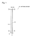
- Fig. 1 is a side view showing a structure of an antenna device of the first exemplary embodiment of the present invention.
- Fig. 2 is a top view showing a structure of an antenna device of the first exemplary embodiment of the present invention.
- an antenna device 10 according to the first exemplary embodiment of the present invention includes a conductor plate 101 touching a ground plate and a dielectric substrate 110 placed on the conductor plate 101 in a stacked manner in a thickness wise direction. However, it may be configured like a multilayer substrate by further increasing the number of layers. As shown in Fig.
- the antenna device 10 has at least two antenna elements 102 and 103, and each of the antenna elements 102 and 103 is arranged near an end of the conductor plate 101, and electricity is supplied by giving an electric potential difference between the conductor plate 101 and the antenna elements through feeding points 102a and 103a.
- the antenna device 10 further includes a first slotline 104 and a second slotline 105, and a width g2 of the second slotline is wider than a width g1 of the first slotline.
- One end of the first slotline 104 is an opening edge in an edge of the conductor plate 101, the edge belonging to an area between the antenna element 102 and 103, and the other end of the first slotline 104 connects with an end of the second slotline 105, and the other end of the second slotline 105 is short-circuited inside the conductor plate 101.
- the antenna device 10 can be built-in in wireless terminal apparatus such as a personal computer and a cellular phone.
- Fig. 3 is a perspective view showing a structure of wireless terminal apparatus 60 equipped with the antenna device 10. As shown in Fig. 3 , the wireless terminal apparatus 60 possesses a chassis 201 on which various components such as a button and a display are mounted, and the antenna device 10 is housed in the chassis 201 and various electronic circuitries are mounted on it additionally.
- a slotline described in patent document 1 reduces interference between antenna elements by making the line length of a slotline be approximately a length of ⁇ /4, where ⁇ being the wavelength of an electromagnetic wave corresponding to the resonance frequency of the antenna elements, and by making one end of the slotline at a conductor plate end be an open end by short-circuiting the other end inside the conductor plate.
- the first slotline 104 and the second slotline 105 have a stepped impedance structure, and thus input impedance Z step of the first slotline 104 and the second slotline 105 seen from the open end in the end of the conductor plate 101 is expressed by the following formula.
- Z slot1 and Z slot2 are the characteristic impedance of the first slotline 104 and the second slotline 105, respectively, and l 1 and l 2 are length l 1 of the first slotline and length l 2 of the second slotline, respectively.
- ⁇ is the propagation coefficient of a radio wave which propagates a slotline, and is expressed in Formula (2).
- Z step should just meet the following formula.
- a formula Z slot1 ⁇ Z slot2 holds because the width g 2 of the second slotline is wider than the width g 1 of the first slotline. Therefore, the left side of Formula (4) takes a numerical value smaller than 1. As a result, there will exist combinations by which the total line length l 1 + l 2 becomes smaller than ⁇ /4 among combinations or l 1 and l 2 which satisfy Formula (4), and it becomes possible to reduce the line length of the slotlines.
- Fig. 4 there is shown a result of electromagnetic field simulation having been performed to S 21 parameter between ports which supply electricity to two antenna elements in a substrate end about respective cases of: when there is no slotline; when there is a slotline of a length of ⁇ /4 of wavelength ⁇ of the resonance frequency of the antenna elements; and when there is a slotline of the exemplary embodiment of the present invention.
- each parameter at the time of the electromagnetic field simulation is as follows. That is, the conductor plate 101 is copper, the dielectric constant of the dielectric substrate 110 is 2.2, lengthwise length L of the conductor plate and the dielectric substrate is 204 mm, lateral length W of the conductor plate and the dielectric substrate is 200 mm, thickness d1 of the conductor plate is 30 ⁇ m and the thickness d2 of the dielectric substrate is 1 mm.
- the antenna elements 102 and 103 use antenna elements having a reverse-F shape as shown in Fig. 2 , and their resonance frequency is 2.4 GHz. There is a distance of 65 mm between the feeding points of the respective antenna elements, and each of a slotline of a ⁇ /4 length and a slotline of this exemplary embodiment is arranged almost in the center between the antenna elements in a similar fashion.
- the slotline of ⁇ /4 length has a width of 0.5 mm, and the width g 2 and the width g 1 of the first slotline and the second slotline of this exemplary embodiment are 0.5 mm and 5 mm, respectively.
- the slotline of ⁇ /4 length has a length of 26.25 mm, and both of the length l 1 of the first slotline and the length l 2 of the second slotline of this exemplary embodiment are 7.35 mm.
- S 21 parameters in the slotline of ⁇ /4 length and the slotline of this exemplary embodiment are almost equal in the resonance frequency 2.4 GHz of the antenna elements. Therefore, it is confirmed that, in a slotline of the exemplary embodiment of the present invention, a total line length of the slotline required to suppress coupling between antenna elements can be made short compared with a slotline of ⁇ /4 length.
- inhibiting effect of interference between antenna elements can be obtained with the total line length l 1 + l 2 of the first slotline 104 and the second slotline 105 that is a numerical value smaller than ⁇ /4. Therefore, in this exemplary embodiment, there can be realized an antenna device which can obtain antenna characteristics to sufficiently reduce interference between antenna elements and which can achieve space-saving or miniaturization, and wireless terminal apparatus using this.
- the first term of Formula (5) at that time becomes a minimum value, and, at the same time, total line length l 1 + l 2 also becomes a minimum value. Accordingly, a structure that satisfies Formula (4) and Formula (6) is most desirable. In this regard, however, in this exemplary embodiment, Formula (4) should be met approximately, and a structure is not limited to a structure that satisfies Formula (6).
- a structure that makes the length of the exclusive-use space of a slotline in the conductor plate 101 in the inward direction shorter is also possible by bending the first slotline 104 and the second slotline 105 on the way at least once.
- Fig. 4 is a top view showing the antenna device 10' of a modification of an antenna device of the first exemplary embodiment of the present invention. Also in this case, a suppression effect of interference between the antenna elements is realized when the length l 1 and l 2 that can be regarded as the line lengths of the first slotline 104 and the second slotline 105 satisfy Formula (4) approximately.
- an antenna device which can achieve miniaturization and space-saving while keeping a given characteristics as an antenna element and wireless terminal apparatus using this can be provided by the first exemplary embodiment of the present invention because interference between the antenna element can be reduced in a state that the total line length of the first slotline and the second slotline is shorter than a case when a slotline of a line length of a length of 1/4 of the wavelength corresponding to the resonance frequency of an antenna element is formed.
- Fig. 6 is a top view showing a structure of an antenna device 20 of the second exemplary embodiment of the present invention.
- Different points of the antenna device 20 from the antenna device 10 of the first exemplary embodiment are: a point that the width g 1 of a first slotline and the width g 2 of a second slotline may be equal; and a point that a conductor part 301a and a conductor parts 301b, at least part of which oppose each other, are arranged further in the neighborhoods of the opposing conductor plate ends which form the slotline 104, and thus the other components are similar.
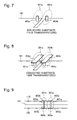
- FIG. 7 is a perspective view of the conductor parts 301a and 301b seen from the side of the dielectric substrate 110, and the dielectric substrate 110 is transparentized for simplification.
- the conductor parts 301a and 301b include at least one piece of conductor via 401 a and at least one piece of conductor via 401b, respectively, arranged in the dielectric substrate 110, and they are connected with the conductor plate 101 and are opposing each other.
- a point that total line length l 1 + l 2 of slotlines will be a minimum value by satisfying Formula (6); and a point that a structure similar to Fig. 5 , which makes a length that all slotlines exclusively possess in the inward direction in the conductor plate 101 short by bending the first slotline 104 and the second slotline 105 on the way, is possible.
- a structure to form conductor plates 402a and 402b that are connected to the conductor vias 401a and 401b and are made to oppose each other into ends of the conductor via 401a and 401b opposite to ends connected to the conductor plate 101 is possible.
- the numerical value of the left side of Formula (4) can be made smaller by making Z slot1 smaller, and total line length l 1 + l 2 can be made shorter by this.
- an antenna device which can achieve space-saving or miniaturization while keeping given characteristics as an antenna element and wireless terminal apparatus using this can be provided, because interference between antenna elements can be reduced in a state that the total line length of the first slotline and the second slotline is shorter than a case where a slotline of a line length of 1/4 length of the wavelength corresponding to the resonance frequency of the antenna elements is formed.
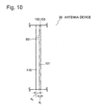
- Fig. 10 is a side view showing a structure of an antenna device 30 of the third exemplary embodiment of the present invention.
- Fig. 11 is a top view showing a structure of the antenna device 30 of the third exemplary embodiment of the present invention.
- the antenna device 30 is different from the antenna device 10 of the first exemplary embodiment: in a point that the width g 1 of the first slotline and the width g 2 of the second slotline may be equal; and in a point that at least one or more pieces of through-hole 501 are further formed in the dielectric substrate 110 that overlaps with the gap part of the second slotline 105, and the other components are similar.
- the point that the total line length l 1 + l 2 of slotlines will be a minimum value by satisfying Formula (6); and the point that a structure similar to Fig. 5 that makes a length that all slotlines exclusively possess in the inward direction in the conductor plate 101 short by bending the first slotline 104 and the second slotline 105 on the way is possible.
- an antenna device which can achieve space-saving or miniaturization while keeping given characteristics as an antenna element and wireless terminal apparatus using this can be provided, because interference between antenna elements can be reduced in a state that the total line length of the first slotline and the second slotline is shorter than a case where a slotline of a line length of 1/4 length of the wavelength corresponding to the resonance frequency of the antenna elements is formed.
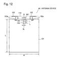
- Fig. 12 is a top view showing a structure of an antenna device of the fourth exemplary embodiment of the present invention.
- An antenna device 40 is different from the antenna device 10 of the first exemplary embodiment: in a point that the width g 1 of the first slotline and the width g 2 of the second slotline may be equal; and in a point that a dielectric part 601 having a dielectric constant larger than the dielectric constant of the dielectric substrate 110 is filled into at least part of a region among the gap part of the slotline 104 and its neighborhood spaces except for the conductor plate 101, and thus the other components are similar.
- the dielectric part 601 By the dielectric part 601, a capacitance between the opposing edges of the conductor plate 101 that form the first slotline 104 is increased. Therefore, characteristic impedance Z slot1 of the first slotline 104 becomes smaller than characteristic impedance Z slot2 of the second slotline 105. Accordingly, the same effect as the first exemplary embodiment can be obtained because the first slotline 104 and the second slotline 105 become a stepped impedance structure, and the left side of Formula (4) becomes smaller than 1.
- a point that the total line length l 1 + l 2 of slotlines will be a minimum value by satisfying Formula (6); and a point that a structure similar to Fig. 5 that makes a length that all slotlines exclusively possess in the inward direction in the conductor plate 101 short by bending the first slotline 104 and the second slotline 105 on the way is possible.
- an antenna device which can achieve space-saving or miniaturization while keeping given characteristics as an antenna element and wireless terminal apparatus using this can be provided, because interference between antenna elements can be reduced in a state that the total line length of the first slotline and the second slotline is shorter than a case where a slotline of a line length of 1/4 length of the wavelength corresponding to the resonance frequency of the antenna elements is formed.
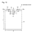
- Fig. 13 is a top view showing a structure of an antenna device of the fifth exemplary embodiment of the present invention.
- An antenna device 50 is different from the antenna device 10 of the first exemplary embodiment: in a point that the width g 1 of the first slotline and the width g 2 of the second slotline may be equal; and in a point that a magnetic substance part 701 having a magnetic permeability larger than the magnetic permeability of the dielectric substrate 110 is filled into at least part of a region among the gap part of the slotline 105 and its neighborhood spaces except for the conductor plate 101, and thus the other components are similar.
- a point that the total line length l 1 + l 2 of slotlines will be a minimum value by satisfying Formula (6); and a point that a structure similar to Fig. 5 that makes a length that all slotlines exclusively possess in the conductor plate 101 in the inward direction short by bending the first slotline 104 and the second slotline 105 on the way is possible.
- an antenna device which can achieve space-saving or miniaturization while keeping given characteristics as an antenna element and wireless terminal apparatus using this can be provided, because interference between antenna elements can be reduced in a state that the total line length of the first slotline and the second slotline is shorter than a case where a slotline of a line length of 1/4 length of the wavelength corresponding to the resonance frequency of the antenna elements is formed.
- the present invention relates to an antenna device having a plurality of antenna elements, and, more particularly, to an antenna device which reduces interference between antenna elements and achieves space-saving and miniaturization.
Landscapes
- Engineering & Computer Science (AREA)
- Computer Networks & Wireless Communication (AREA)
- Physics & Mathematics (AREA)
- Electromagnetism (AREA)
- Details Of Aerials (AREA)
- Waveguide Aerials (AREA)
- Support Of Aerials (AREA)
Abstract
Description
- The present invention relates to an antenna device having a plurality of antenna elements and, more particularly, to an antenna device which reduces interference between the antenna elements and achieves space-saving and miniaturization.
- As an antenna device, there is known a diversity antenna which improves the transmission rate of a signal by receiving identical wireless signals separately by a plurality of antenna elements, and using a received signal from an antenna element superior in a radio wave state on a priority basis. Also, recently, as an antenna device, a MIMO (Multi-Input Multi-Output) antenna which improves the transmission rate of a signal dramatically by transmitting or receiving a plurality of different wireless signals within an identical bandwidth simultaneously using a plurality of antenna elements and by increasing the number of channels of a signal as much as the number of the antenna elements is being paid attention.
- When performing wireless communication using a diversity antenna or a MIMO antenna mentioned above, it is said that it is desirable that a plurality of antenna elements are in a low correlation state with each other as much as possible. However, when a plurality of antenna elements are mounted onto a radio apparatus, a radio terminal or the like, a distance between the antenna elements often cannot be separated sufficiently relative to the wavelength of a received radio wave due to restrictions in the size of the apparatus or the terminal and in a space which can be used for the antenna elements. Therefore, there is a problem that a low correlation cannot be realized in such occasions due to electromagnetic interference between a plurality of antenna elements (inter-antenna element interference), and the communication performance of a diversity antenna and a MIMO antenna degrades.
- Accordingly, there is known an electronic apparatus equipped with an antenna device which makes interference between antenna elements be reduced by forming a slotline of a length corresponding to 1/4 wavelength of the resonance frequency of the antenna elements into a portion corresponding to an area between the plurality of antenna elements among end parts of a ground pattern connected to the plurality of antenna elements through feeding points (patent document 1), for example.
- [Patent Literature 1] Japanese Patent Application Laid-Open No.
2008-283464 - However, in an antenna described in
patent literature 1, there is caused a problem that, when a slotline is provided in an end part of a ground pattern, an installation space for various devices installed on the ground pattern becomes small due to a space corresponding to the length of the slotline because the slotline of the length of 1/4 wavelength corresponding to the resonance frequency of the antenna elements is needed to be formed,. - The present invention has been made in view of the above-mentioned problem, and its object is to provide an antenna device which can achieve space-saving or miniaturization while keeping given characteristics as an antenna element by reducing interference between antenna elements and wireless terminal apparatus using this.
- One aspect of the present invention for achieving the above-mentioned object is an antenna device that comprises: a conductor plate; at least two antenna elements arranged near an end of the conductor plate; a first slotline formed into the conductor plate, the first slotline having a characteristic impedance of an optional numerical value Z1; a second slotline formed into the conductor plate, the second slotline having a characteristic impedance of an optional numerical value Z2 larger than Z1; one end of the first slotline being an open end in an area between the antenna elements within the conductor plate end; the other end of the first slotline connecting with one end of the second slotline; and the other end of the second slotline being short-circuited inside the conductor plate, and wireless terminal apparatus using this.
- An antenna device which can achieve space-saving or miniaturization while keeping given characteristics as an antenna element by reducing interference between antenna elements and wireless terminal apparatus using this can be provided because interference between the antenna elements can be reduced in a state that the total line length of a first slotline and a second slotline is shorter than a case when a slotline of a line length of 1/4 length of the wavelength corresponding to the resonance frequency of the antenna elements is formed.
-
- [
Fig. 1] Fig. 1 is a side view showing a structure of an antenna device of a first exemplary embodiment of the present invention. - [
Fig. 2] Fig. 2 is a top view showing a structure of an antenna device of the first exemplary embodiment of the present invention. - [
Fig. 3] Fig. 3 is a perspective view showing a structure of wireless terminal apparatus equipped with an antenna device of the first exemplary embodiment of the present invention. - [
Fig. 4] Fig. 4 is a diagram showing a result of simulation about S21 parameter of an antenna device of the first exemplary embodiment of the present invention. - [
Fig. 5] Fig. 5 is a top view showing a structure of an antenna device of the first exemplary embodiment of the present invention. - [
Fig. 6] Fig. 6 is a top view showing a structure of an antenna device of a second exemplary embodiment of the present invention. - [
Fig. 7] Fig. 7 is a perspective view showing a structure of a conductor part of an antenna device of the second exemplary embodiment of the present invention. - [
Fig. 8] Fig. 8 is a perspective view showing a structure of a conductor part of an antenna device of the second exemplary embodiment of the present invention. - [
Fig. 9] Fig. 9 is a side view showing a structure of a conductor part of an antenna device of the second exemplary embodiment of the present invention. - [
Fig. 10] Fig. 10 is a side view showing a structure of an antenna device of a third exemplary embodiment of the present invention. - [
Fig. 11] Fig. 11 is a top view showing a structure of an antenna device of the third exemplary embodiment of the present invention. - [
Fig. 12] Fig. 12 is a top view showing a structure of an antenna device of a fourth exemplary embodiment of the present invention. - [
Fig. 13] Fig. 13 is a top view showing a structure of an antenna device of a fifth exemplary embodiment of the present invention. - Hereinafter, an exemplary embodiment of the present invention will be described in detail with reference to a drawing. However, although technically preferred limitation to carry out the present invention is made to the exemplary embodiments described below, it does not limit the scope of the invention as below.
-
Fig. 1 is a side view showing a structure of an antenna device of the first exemplary embodiment of the present invention.Fig. 2 is a top view showing a structure of an antenna device of the first exemplary embodiment of the present invention. As shown inFig. 1 , anantenna device 10 according to the first exemplary embodiment of the present invention includes aconductor plate 101 touching a ground plate and adielectric substrate 110 placed on theconductor plate 101 in a stacked manner in a thickness wise direction. However, it may be configured like a multilayer substrate by further increasing the number of layers. As shown inFig. 2 , theantenna device 10 has at least twoantenna elements antenna elements conductor plate 101, and electricity is supplied by giving an electric potential difference between theconductor plate 101 and the antenna elements throughfeeding points - The
antenna device 10 further includes afirst slotline 104 and asecond slotline 105, and a width g2 of the second slotline is wider than a width g1 of the first slotline. One end of thefirst slotline 104 is an opening edge in an edge of theconductor plate 101, the edge belonging to an area between theantenna element first slotline 104 connects with an end of thesecond slotline 105, and the other end of thesecond slotline 105 is short-circuited inside theconductor plate 101. - The
antenna device 10 can be built-in in wireless terminal apparatus such as a personal computer and a cellular phone.Fig. 3 is a perspective view showing a structure of wireless terminal apparatus 60 equipped with theantenna device 10. As shown inFig. 3 , the wireless terminal apparatus 60 possesses achassis 201 on which various components such as a button and a display are mounted, and theantenna device 10 is housed in thechassis 201 and various electronic circuitries are mounted on it additionally. - Hereinafter, an action and an effect of the exemplary embodiment of the present invention will be described.
- When a slotline having an open end in an end of a conductor plate is formed in the neighborhood of the conductor plate end corresponding to an area between a plurality of antenna elements arranged in the conductor plate end, inter-antenna element interference is reduced. A slotline described in
patent document 1 reduces interference between antenna elements by making the line length of a slotline be approximately a length of λ/4, where λ being the wavelength of an electromagnetic wave corresponding to the resonance frequency of the antenna elements, and by making one end of the slotline at a conductor plate end be an open end by short-circuiting the other end inside the conductor plate. - On the other hand, in the exemplary embodiment of the present invention, the
first slotline 104 and thesecond slotline 105 have a stepped impedance structure, and thus input impedance Zstep of thefirst slotline 104 and thesecond slotline 105 seen from the open end in the end of theconductor plate 101 is expressed by the following formula.

- Here, Zslot1 and Zslot2 are the characteristic impedance of the
first slotline 104 and thesecond slotline 105, respectively, and l1 and l2 are length l1 of the first slotline and length l2 of the second slotline, respectively. Also, β is the propagation coefficient of a radio wave which propagates a slotline, and is expressed in Formula (2). - Because the opening of the
first slotline 104 has only to be an open end at an end portion of theconductor plate 101 to suppress interference between theantenna elements 
- Therefore, from Formula (1) and Formula (3), the following only has to hold.

- In this exemplary embodiment, a formula Zslot1 < Zslot2 holds because the width g2 of the second slotline is wider than the width g1 of the first slotline. Therefore, the left side of Formula (4) takes a numerical value smaller than 1. As a result, there will exist combinations by which the total line length l1 + l2 becomes smaller than λ/4 among combinations or l1 and l2 which satisfy Formula (4), and it becomes possible to reduce the line length of the slotlines.
- In
Fig. 4 , there is shown a result of electromagnetic field simulation having been performed to S21 parameter between ports which supply electricity to two antenna elements in a substrate end about respective cases of: when there is no slotline; when there is a slotline of a length of λ/4 of wavelength λ of the resonance frequency of the antenna elements; and when there is a slotline of the exemplary embodiment of the present invention. - Each parameter at the time of the electromagnetic field simulation is as follows. That is, the
conductor plate 101 is copper, the dielectric constant of thedielectric substrate 110 is 2.2, lengthwise length L of the conductor plate and the dielectric substrate is 204 mm, lateral length W of the conductor plate and the dielectric substrate is 200 mm, thickness d1 of the conductor plate is 30 µm and the thickness d2 of the dielectric substrate is 1 mm. Theantenna elements Fig. 2 , and their resonance frequency is 2.4 GHz. There is a distance of 65 mm between the feeding points of the respective antenna elements, and each of a slotline of a λ/4 length and a slotline of this exemplary embodiment is arranged almost in the center between the antenna elements in a similar fashion. - Regarding a width of a slotline, the slotline of λ/4 length has a width of 0.5 mm, and the width g2 and the width g1 of the first slotline and the second slotline of this exemplary embodiment are 0.5 mm and 5 mm, respectively. About a length of a slotline, the slotline of λ/4 length has a length of 26.25 mm, and both of the length l1 of the first slotline and the length l2 of the second slotline of this exemplary embodiment are 7.35 mm.
- As shown in
Fig. 4 , S21 parameters in the slotline of λ/4 length and the slotline of this exemplary embodiment are almost equal in the resonance frequency 2.4 GHz of the antenna elements. Therefore, it is confirmed that, in a slotline of the exemplary embodiment of the present invention, a total line length of the slotline required to suppress coupling between antenna elements can be made short compared with a slotline of λ/4 length. - As above, in this exemplary embodiment, inhibiting effect of interference between antenna elements can be obtained with the total line length l1 + l2 of the
first slotline 104 and thesecond slotline 105 that is a numerical value smaller than λ/4. Therefore, in this exemplary embodiment, there can be realized an antenna device which can obtain antenna characteristics to sufficiently reduce interference between antenna elements and which can achieve space-saving or miniaturization, and wireless terminal apparatus using this. - Meanwhile, when relational expressions of the arithmetic mean and the geometric mean that are generally known are applied to the left side of Formula (4), the following formula holds.

- The equal sign holds between the first term and the second term of Formula (5) when the following
formula holds. 
- Therefore, the first term of Formula (5) at that time becomes a minimum value, and, at the same time, total line length l1 + l2 also becomes a minimum value. Accordingly, a structure that satisfies Formula (4) and Formula (6) is most desirable. In this regard, however, in this exemplary embodiment, Formula (4) should be met approximately, and a structure is not limited to a structure that satisfies Formula (6).
- Furthermore, as shown in
Fig. 5 , a structure that makes the length of the exclusive-use space of a slotline in theconductor plate 101 in the inward direction shorter is also possible by bending thefirst slotline 104 and thesecond slotline 105 on the way at least once.Fig. 4 is a top view showing the antenna device 10' of a modification of an antenna device of the first exemplary embodiment of the present invention. Also in this case, a suppression effect of interference between the antenna elements is realized when the length l1 and l2 that can be regarded as the line lengths of thefirst slotline 104 and thesecond slotline 105 satisfy Formula (4) approximately. - As above, an antenna device which can achieve miniaturization and space-saving while keeping a given characteristics as an antenna element and wireless terminal apparatus using this can be provided by the first exemplary embodiment of the present invention because interference between the antenna element can be reduced in a state that the total line length of the first slotline and the second slotline is shorter than a case when a slotline of a line length of a length of 1/4 of the wavelength corresponding to the resonance frequency of an antenna element is formed.
-
Fig. 6 is a top view showing a structure of anantenna device 20 of the second exemplary embodiment of the present invention. Different points of theantenna device 20 from theantenna device 10 of the first exemplary embodiment are: a point that the width g1 of a first slotline and the width g2 of a second slotline may be equal; and a point that aconductor part 301a and aconductor parts 301b, at least part of which oppose each other, are arranged further in the neighborhoods of the opposing conductor plate ends which form theslotline 104, and thus the other components are similar. - An enlarged perspective view of the
conductor parts Fig. 7. Fig. 7 is a perspective view of theconductor parts dielectric substrate 110, and thedielectric substrate 110 is transparentized for simplification. Theconductor parts dielectric substrate 110, and they are connected with theconductor plate 101 and are opposing each other. - Hereinafter, an effect of the
conductor parts first slotline 104 due to theconductor parts first slotline 104 becomes smaller than characteristic impedance Zslot2 of thesecond slotline 105. Therefore, the same effect as the first exemplary embodiment can be obtained because thefirst slotline 104 and thesecond slotline 105 form a stepped impedance structure and the left side of Formula (4) becomes smaller than 1. - Also similar to the first exemplary embodiment are: a point that total line length l1 + l2 of slotlines will be a minimum value by satisfying Formula (6); and a point that a structure similar to
Fig. 5 , which makes a length that all slotlines exclusively possess in the inward direction in theconductor plate 101 short by bending thefirst slotline 104 and thesecond slotline 105 on the way, is possible. - Furthermore, as shown in
Fig. 8 , by increasing the number of pieces of the conductor vias 401 a and 401b or by making it a multilayer substrate, a structure to formconductor plates conductor vias conductor plate 101 is possible. - As shown in
Fig. 9 , also possible is a structure that makes characteristic impedance Zslot1 of thefirst slotline 104 further smaller by making areas of opposing conductors between theconductor parts Fig. 7 : providingconductor vias dielectric substrate 120 stacked on a side of theconductor plate 101 opposite to the side of thedielectric substrate 110 in a thickness wise direction, theconductor vias conductor plate 101 and being opposite to each other; and further connectingconductor plates conductor vias conductor plate 101, respectively. The numerical value of the left side of Formula (4) can be made smaller by making Zslot1 smaller, and total line length l1 + l2 can be made shorter by this. - Thus, according to the second exemplary embodiment of the present invention, an antenna device which can achieve space-saving or miniaturization while keeping given characteristics as an antenna element and wireless terminal apparatus using this can be provided, because interference between antenna elements can be reduced in a state that the total line length of the first slotline and the second slotline is shorter than a case where a slotline of a line length of 1/4 length of the wavelength corresponding to the resonance frequency of the antenna elements is formed.
-
Fig. 10 is a side view showing a structure of anantenna device 30 of the third exemplary embodiment of the present invention.Fig. 11 is a top view showing a structure of theantenna device 30 of the third exemplary embodiment of the present invention. - The
antenna device 30 is different from theantenna device 10 of the first exemplary embodiment: in a point that the width g1 of the first slotline and the width g2 of the second slotline may be equal; and in a point that at least one or more pieces of through-hole 501 are further formed in thedielectric substrate 110 that overlaps with the gap part of thesecond slotline 105, and the other components are similar. - Hereinafter, an effect of the through-
hole 501 which is the feature of this exemplary embodiment will be described. By the through-hole 501, an effective dielectric constant in the space between the opposing conductor parts of thesecond slotline 105 declines, and as a result, characteristic impedance Zslot2 of thesecond slotline 105 becomes larger than characteristic impedance Zslot1 of thefirst slotline 104. Therefore, the same effect as the first exemplary embodiment can be obtained because thefirst slotline 104 and thesecond slotline 105 becomes a stepped impedance structure, and the left side of Formula (4) becomes smaller than 1. - Also similar to the first exemplary embodiment are: the point that the total line length l1 + l2 of slotlines will be a minimum value by satisfying Formula (6); and the point that a structure similar to
Fig. 5 that makes a length that all slotlines exclusively possess in the inward direction in theconductor plate 101 short by bending thefirst slotline 104 and thesecond slotline 105 on the way is possible. - Thus, according to the third exemplary embodiment of the present invention, an antenna device which can achieve space-saving or miniaturization while keeping given characteristics as an antenna element and wireless terminal apparatus using this can be provided, because interference between antenna elements can be reduced in a state that the total line length of the first slotline and the second slotline is shorter than a case where a slotline of a line length of 1/4 length of the wavelength corresponding to the resonance frequency of the antenna elements is formed.
-
Fig. 12 is a top view showing a structure of an antenna device of the fourth exemplary embodiment of the present invention. - An
antenna device 40 is different from theantenna device 10 of the first exemplary embodiment: in a point that the width g1 of the first slotline and the width g2 of the second slotline may be equal; and in a point that adielectric part 601 having a dielectric constant larger than the dielectric constant of thedielectric substrate 110 is filled into at least part of a region among the gap part of theslotline 104 and its neighborhood spaces except for theconductor plate 101, and thus the other components are similar. - Hereinafter, an effect of the
dielectric part 601 will be described. By thedielectric part 601, a capacitance between the opposing edges of theconductor plate 101 that form thefirst slotline 104 is increased. Therefore, characteristic impedance Zslot1 of thefirst slotline 104 becomes smaller than characteristic impedance Zslot2 of thesecond slotline 105. Accordingly, the same effect as the first exemplary embodiment can be obtained because thefirst slotline 104 and thesecond slotline 105 become a stepped impedance structure, and the left side of Formula (4) becomes smaller than 1. - Also similar to the first exemplary embodiment are: a point that the total line length l1 + l2 of slotlines will be a minimum value by satisfying Formula (6); and a point that a structure similar to
Fig. 5 that makes a length that all slotlines exclusively possess in the inward direction in theconductor plate 101 short by bending thefirst slotline 104 and thesecond slotline 105 on the way is possible. - Thus, according to the fourth exemplary embodiment of the present invention, an antenna device which can achieve space-saving or miniaturization while keeping given characteristics as an antenna element and wireless terminal apparatus using this can be provided, because interference between antenna elements can be reduced in a state that the total line length of the first slotline and the second slotline is shorter than a case where a slotline of a line length of 1/4 length of the wavelength corresponding to the resonance frequency of the antenna elements is formed.
-
Fig. 13 is a top view showing a structure of an antenna device of the fifth exemplary embodiment of the present invention. Anantenna device 50 is different from theantenna device 10 of the first exemplary embodiment: in a point that the width g1 of the first slotline and the width g2 of the second slotline may be equal; and in a point that amagnetic substance part 701 having a magnetic permeability larger than the magnetic permeability of thedielectric substrate 110 is filled into at least part of a region among the gap part of theslotline 105 and its neighborhood spaces except for theconductor plate 101, and thus the other components are similar. - Hereinafter, an effect of the
magnetic substance part 701 will be described. By themagnetic substance part 701, a series inductance of thesecond slotline 105 as a transmission line increase. Therefore, characteristic impedance Zslot2 of thesecond slotline 105 becomes larger than characteristic impedance Zslot1 of thefirst slotline 104. Accordingly, the same effect as the first exemplary embodiment can be obtained because thefirst slotline 104 and thesecond slotline 105 become a stepped impedance structure, and the left side of Formula (4) becomes smaller than 1. - Also similar to the first exemplary embodiment are: a point that the total line length l1 + l2 of slotlines will be a minimum value by satisfying Formula (6); and a point that a structure similar to
Fig. 5 that makes a length that all slotlines exclusively possess in theconductor plate 101 in the inward direction short by bending thefirst slotline 104 and thesecond slotline 105 on the way is possible. - Thus, according to the fifth exemplary embodiment of the present invention, an antenna device which can achieve space-saving or miniaturization while keeping given characteristics as an antenna element and wireless terminal apparatus using this can be provided, because interference between antenna elements can be reduced in a state that the total line length of the first slotline and the second slotline is shorter than a case where a slotline of a line length of 1/4 length of the wavelength corresponding to the resonance frequency of the antenna elements is formed.
- Meanwhile, the first, second, third, fourth and fifth exemplary embodiments mentioned above can be combined within a range where their contents do not disagree with each other. Various modifications of the present invention are possible within the scope of the invention described in the claims without limiting to the above-mentioned exemplary embodiments, and it goes without saying that those are also included within the scope of the present invention.
- This application claims priority based on Japanese application Japanese Patent Application No.
2012-064789 filed on March 22, 2012 - The present invention relates to an antenna device having a plurality of antenna elements, and, more particularly, to an antenna device which reduces interference between antenna elements and achieves space-saving and miniaturization.
-
- 10, 10', 20, 30, 40 and 50 Antenna device
- 60 Wireless terminal apparatus
- 101 Conductor plate
- 102 and 103 Antenna element
- 102a and 103a Feeding point
- 104 First slotline
- 105 Second slotline
- 110 and 120 Dielectric substrate
- 201 Chassis
- 301a and 301b Conductor part
- 401a, 401b, 403a and 403b Conductor via (those are included in 301a and 301b)
- 402a, 402b, 404a and 404b Conductor plate (those are included in 301a and 301b)
- 501 Through-hole
- 601 Dielectric part
- 701 Magnetic substance part
- d1 Thickness of a conductor plate
- d2 Thickness of a dielectric substrate
- L Lengthwise length of a conductor plate and a dielectric substrate
- W Lateral length of a conductor plate and a dielectric substrate
- l1 Length of a first slotline
- l2 Length of a second slotline
- g1 Width of a first slotline
- g2 Width of a second slotline
Claims (10)
- An antenna device, comprising:a conductor plate; at least two antenna elements arranged near an end of said conductor plate; a first slotline formed into said conductor plate, said first slotline having a characteristic impedance of an optional numerical value Z1; a second slotline formed into said conductor plate, said second slotline having a characteristic impedance of an optional numerical value Z2 larger than Z1; one end of said first slotline being an open end in an area between said antenna elements within said conductor plate end; an other end of said first slotline connecting with one end of said second slotline; and an other end of said second slotline being short-circuited inside said conductor plate.
- The antenna device according to claim 1, wherein
a width of said second slotline is wider than a width of said first slotline. - The antenna device according to claim 1 or 2, further comprising:conductor parts A 1 and B 1 in a neighborhood of each of areas A and B near opposing ends of said conductor plate forming said first slotline, at least part of said conductor parts A1 and B1 opposing each other; said conductor parts A1 and B1 being connected to said areas A and B of said conductor plate end, respectively; and said conductor parts A1 and B1 not being connected with each other.
- The antenna device according to any one of claims 1 to 3, wherein
a substance having a dielectric constant larger than an effective dielectric constant of a gap part of said first slotline is filled into at least part of said gap part of said first slotline further. - The antenna device according to any one of claims 1 to 4, wherein
a substance having a magnetic permeability larger than an effective magnetic permeability of a gap part of said second slotline is filled into at least part of said gap part of said second slotline and in near spaces except for said conductor plate further. - The antenna device according to any one of claims 1 to 5, wherein
said conductor plate is installed on a dielectric substrate. - The antenna device according to any one of claims 1 to 6, wherein
at least one through-hole is provided in an area of said dielectric substrate overlapping said gap part of said second slotline. - The antenna device according to any one of claims 1 to 7, wherein
at least part of said first and said second slotline is of a bent shape. - The antenna device according to any one of claims 1 to 8, wherein
said first slotline and said second slotline have lengths capable of being assumed to be approximately identical. - A wireless terminal apparatus comprising an antenna device according to any one of claims 1 to 9.
Applications Claiming Priority (2)
| Application Number | Priority Date | Filing Date | Title |
|---|---|---|---|
| JP2012064789 | 2012-03-22 | ||
| PCT/JP2013/001767 WO2013140770A1 (en) | 2012-03-22 | 2013-03-15 | Antenna device and wireless terminal device using same |
Publications (2)
| Publication Number | Publication Date |
|---|---|
| EP2830154A1 true EP2830154A1 (en) | 2015-01-28 |
| EP2830154A4 EP2830154A4 (en) | 2015-11-11 |
Family
ID=49222252
Family Applications (1)
| Application Number | Title | Priority Date | Filing Date |
|---|---|---|---|
| EP13765079.2A Withdrawn EP2830154A4 (en) | 2012-03-22 | 2013-03-15 | Antenna device and wireless terminal device using same |
Country Status (4)
| Country | Link |
|---|---|
| US (1) | US20150002367A1 (en) |
| EP (1) | EP2830154A4 (en) |
| JP (1) | JPWO2013140770A1 (en) |
| WO (1) | WO2013140770A1 (en) |
Cited By (1)
| Publication number | Priority date | Publication date | Assignee | Title |
|---|---|---|---|---|
| CN107408757A (en) * | 2015-03-26 | 2017-11-28 | 微软技术许可有限责任公司 | Antenna is isolated |
Families Citing this family (11)
| Publication number | Priority date | Publication date | Assignee | Title |
|---|---|---|---|---|
| US10505269B2 (en) * | 2013-04-28 | 2019-12-10 | The Board Of Trustees Of The University Of Alabama For And On Behalf Of The University Of Alabama | Magnetic antenna structures |
| JP5941504B2 (en) * | 2014-07-23 | 2016-06-29 | レノボ・シンガポール・プライベート・リミテッド | Electronic device antenna system and method for enhancing isolation |
| US10431891B2 (en) | 2015-12-24 | 2019-10-01 | Intel IP Corporation | Antenna arrangement |
| JP6573326B2 (en) * | 2017-01-23 | 2019-09-11 | Necプラットフォームズ株式会社 | Wireless communication apparatus and noise suppression method |
| JP6865072B2 (en) * | 2017-03-13 | 2021-04-28 | 株式会社パナソニックシステムネットワークス開発研究所 | Antenna device and electronic device equipped with an antenna device |
| US10615486B2 (en) * | 2017-06-28 | 2020-04-07 | Intel IP Corporation | Antenna system |
| US11276925B2 (en) * | 2018-01-31 | 2022-03-15 | Dell Products, Lp | System and method for establishing and operating plural antenna systems in proximity |
| KR102608773B1 (en) * | 2019-02-14 | 2023-12-04 | 삼성전자주식회사 | Antenna module and electronic device including the same |
| CN115224482B (en) * | 2021-04-16 | 2025-07-25 | 台达电子工业股份有限公司 | Antenna structure and wireless communication device |
| US11996623B2 (en) * | 2021-12-31 | 2024-05-28 | Schlage Lock Company Llc | UWB antenna solutions for increased accuracy for intent detection in access control systems |
| CN220914575U (en) * | 2023-09-21 | 2024-05-07 | 智邦科技股份有限公司 | Antenna module |
Family Cites Families (9)
| Publication number | Priority date | Publication date | Assignee | Title |
|---|---|---|---|---|
| GB0114818D0 (en) * | 2001-06-18 | 2001-08-08 | Nokia Corp | Conductor structure |
| JP2007013643A (en) * | 2005-06-30 | 2007-01-18 | Lenovo Singapore Pte Ltd | Integrated flat multi-element antenna and electronic equipment |
| US7764236B2 (en) * | 2007-01-04 | 2010-07-27 | Apple Inc. | Broadband antenna for handheld devices |
| JP4738380B2 (en) | 2007-05-10 | 2011-08-03 | 株式会社東芝 | Electronics |
| US8441404B2 (en) * | 2007-12-18 | 2013-05-14 | Apple Inc. | Feed networks for slot antennas in electronic devices |
| JP2010161715A (en) * | 2009-01-09 | 2010-07-22 | Panasonic Corp | Portable radio |
| US8085202B2 (en) * | 2009-03-17 | 2011-12-27 | Research In Motion Limited | Wideband, high isolation two port antenna array for multiple input, multiple output handheld devices |
| EP2408062A1 (en) * | 2010-07-12 | 2012-01-18 | Research In Motion Limited | Multiple input - multiple output antenna module |
| WO2012008946A1 (en) * | 2010-07-12 | 2012-01-19 | Research In Motion Limited | Multiple input - multiple output antenna module |
-
2013
- 2013-03-15 US US14/375,179 patent/US20150002367A1/en not_active Abandoned
- 2013-03-15 JP JP2014506030A patent/JPWO2013140770A1/en active Pending
- 2013-03-15 EP EP13765079.2A patent/EP2830154A4/en not_active Withdrawn
- 2013-03-15 WO PCT/JP2013/001767 patent/WO2013140770A1/en not_active Ceased
Cited By (1)
| Publication number | Priority date | Publication date | Assignee | Title |
|---|---|---|---|---|
| CN107408757A (en) * | 2015-03-26 | 2017-11-28 | 微软技术许可有限责任公司 | Antenna is isolated |
Also Published As
| Publication number | Publication date |
|---|---|
| WO2013140770A1 (en) | 2013-09-26 |
| EP2830154A4 (en) | 2015-11-11 |
| US20150002367A1 (en) | 2015-01-01 |
| JPWO2013140770A1 (en) | 2015-08-03 |
Similar Documents
| Publication | Publication Date | Title |
|---|---|---|
| EP2830154A1 (en) | Antenna device and wireless terminal device using same | |
| EP2535979B1 (en) | Directional coupler | |
| US9312608B2 (en) | Multiple-input multiple-output antenna device | |
| JP6137246B2 (en) | High frequency filter, high frequency diplexer, and electronic device | |
| US9917357B2 (en) | Antenna system | |
| US10445635B2 (en) | Feeder coil, antenna device, and electronic appliance | |
| US9105975B2 (en) | Antenna device and portable wireless terminal equipped with the same | |
| CN103141031B (en) | Impedance converting circuit and communication terminal apparatus | |
| US9509049B2 (en) | Magnetic antenna, antenna device, and electronic apparatus | |
| US20130285870A1 (en) | Antenna apparatus and electronic device including antenna apparatus | |
| US20130057446A1 (en) | Antenna device and portable wireless terminal equipped with the same | |
| EP3327859B1 (en) | Directional coupler and communication module | |
| KR20110121792A (en) | Beauty antenna device | |
| EP2081250A1 (en) | Antenna device and electronic apparatus using the same | |
| US20130135154A1 (en) | Portable wireless device | |
| US20160211563A1 (en) | Structure and electronic circuit | |
| US20150255863A1 (en) | Antenna device | |
| US20160072194A1 (en) | Mimo antenna device | |
| US10637123B2 (en) | Directional coupler | |
| CN206180068U (en) | Flexible cable for high-frequency front-end, high-frequency front-end component, and electronic equipment | |
| US20230411846A1 (en) | Decoupling circuit | |
| US9859598B2 (en) | Electronic circuit | |
| JP5084678B2 (en) | Power divider circuit, element thereof, and circuit board and circuit module provided with the circuit | |
| EP2566050A1 (en) | Composite component | |
| JP2016100797A (en) | Filter integrated coupler and communication module |
Legal Events
| Date | Code | Title | Description |
|---|---|---|---|
| PUAI | Public reference made under article 153(3) epc to a published international application that has entered the european phase |
Free format text: ORIGINAL CODE: 0009012 |
|
| 17P | Request for examination filed |
Effective date: 20140821 |
|
| AK | Designated contracting states |
Kind code of ref document: A1 Designated state(s): AL AT BE BG CH CY CZ DE DK EE ES FI FR GB GR HR HU IE IS IT LI LT LU LV MC MK MT NL NO PL PT RO RS SE SI SK SM TR |
|
| AX | Request for extension of the european patent |
Extension state: BA ME |
|
| DAX | Request for extension of the european patent (deleted) | ||
| RA4 | Supplementary search report drawn up and despatched (corrected) |
Effective date: 20151008 |
|
| RIC1 | Information provided on ipc code assigned before grant |
Ipc: H01Q 1/48 20060101ALI20151002BHEP Ipc: H01Q 1/52 20060101AFI20151002BHEP Ipc: H01Q 21/28 20060101ALI20151002BHEP Ipc: H01Q 13/08 20060101ALI20151002BHEP Ipc: H01Q 1/24 20060101ALI20151002BHEP Ipc: H01Q 9/42 20060101ALI20151002BHEP |
|
| STAA | Information on the status of an ep patent application or granted ep patent |
Free format text: STATUS: THE APPLICATION IS DEEMED TO BE WITHDRAWN |
|
| 18D | Application deemed to be withdrawn |
Effective date: 20160507 |