EP2828676B1 - Simple microwave field imaging device - Google Patents
Simple microwave field imaging device Download PDFInfo
- Publication number
- EP2828676B1 EP2828676B1 EP13717444.7A EP13717444A EP2828676B1 EP 2828676 B1 EP2828676 B1 EP 2828676B1 EP 13717444 A EP13717444 A EP 13717444A EP 2828676 B1 EP2828676 B1 EP 2828676B1
- Authority
- EP
- European Patent Office
- Prior art keywords
- microwave
- atoms
- magnetic field
- cell
- hyperfine
- Prior art date
- Legal status (The legal status is an assumption and is not a legal conclusion. Google has not performed a legal analysis and makes no representation as to the accuracy of the status listed.)
- Active
Links
Images


Classifications
-
- G—PHYSICS
- G01—MEASURING; TESTING
- G01R—MEASURING ELECTRIC VARIABLES; MEASURING MAGNETIC VARIABLES
- G01R33/00—Arrangements or instruments for measuring magnetic variables
- G01R33/20—Arrangements or instruments for measuring magnetic variables involving magnetic resonance
- G01R33/28—Details of apparatus provided for in groups G01R33/44 - G01R33/64
- G01R33/32—Excitation or detection systems, e.g. using radio frequency signals
- G01R33/323—Detection of MR without the use of RF or microwaves, e.g. force-detected MR, thermally detected MR, MR detection via electrical conductivity, optically detected MR
-
- G—PHYSICS
- G01—MEASURING; TESTING
- G01R—MEASURING ELECTRIC VARIABLES; MEASURING MAGNETIC VARIABLES
- G01R33/00—Arrangements or instruments for measuring magnetic variables
- G01R33/02—Measuring direction or magnitude of magnetic fields or magnetic flux
- G01R33/10—Plotting field distribution ; Measuring field distribution
-
- G—PHYSICS
- G01—MEASURING; TESTING
- G01R—MEASURING ELECTRIC VARIABLES; MEASURING MAGNETIC VARIABLES
- G01R33/00—Arrangements or instruments for measuring magnetic variables
- G01R33/12—Measuring magnetic properties of articles or specimens of solids or fluids
- G01R33/1284—Spin resolved measurements; Influencing spins during measurements, e.g. in spintronics devices
-
- G—PHYSICS
- G01—MEASURING; TESTING
- G01R—MEASURING ELECTRIC VARIABLES; MEASURING MAGNETIC VARIABLES
- G01R33/00—Arrangements or instruments for measuring magnetic variables
- G01R33/20—Arrangements or instruments for measuring magnetic variables involving magnetic resonance
- G01R33/44—Arrangements or instruments for measuring magnetic variables involving magnetic resonance using nuclear magnetic resonance [NMR]
- G01R33/48—NMR imaging systems
Definitions
- the invention relates to a device for sensing (e.g. imaging) at least one microwave magnetic field polarization component of a microwave field as well as to a method for sensing such a component.
- the problem underlying the present invention is to provide for a device for sensing a microwave magnetic field polarization component that is relatively easy to implement.
- a device comprises a preparation means being designed to prepare an atomic vapor comprising a plurality of thermal atoms in a (pre-defined) first hyperfine state, particularly a dark state to applied laser light, which first hyperfine state is split energetically from at least one other hyperfine state due to the zero-field hyperfine splitting and/or due to a static magnetic field B 0 generated by said preparation means, at least one cell for enclosing said plurality of atoms, wherein the microwave (field) comprising said magnetic field polarization component (with respect to the static magnetic field B 0 ) to be sensed (imaged), is able to drive Rabi oscillations of said plurality of thermal atoms between said first hyperfine state and a second hyperfine state, wherein the Rabi frequency of the Rabi oscillations is proportional to said magnetic field polarization component, and an imaging means being designed to generate a state image of said plurality of thermal atoms depending on the spatial atomic hyperfine state density distribution, which in turn is
- the device according to the invention is particularly able to sense/image microwaves of all kinds of (electronic) devices, for instance cell phones, conductors (wave guides) etc.
- the device may also be used to sense a microwave (field) that is generated at a remote place (spaced apart from the device).
- the device may further comprise a microwave generating device (microwave source) for generating said microwave comprising said magnetic field polarization component ( B - , B ⁇ , B + ) relative to the static magnetic field B 0 to be imaged, which microwave is adapted to drive Rabi oscillations of said plurality of thermal atoms between said first hyperfine state and a second hyperfine state, where the Rabi frequency is proportional to said magnetic field polarization component.
- microwave source for generating said microwave comprising said magnetic field polarization component ( B - , B ⁇ , B + ) relative to the static magnetic field B 0 to be imaged, which microwave is adapted to drive Rabi oscillations of said plurality of thermal atoms between said first hyperfine state and a second hyperfine state, where the Rabi frequency is proportional to said magnetic field polarization component.
- such a microwave generating device may be particularly designed to generate microwaves having a variable frequency and/or amplitude, which can be adjusted by means of said microwave generating device.
- such a microwave generating device may be designed to be connected to a separate (interchangeable) microwave device (e.g. a passive microwave device like a waveguide, for instance a coplanar waveguide, or some other passive device, into which a microwave signal is fed by the microwave generating device so as to generate the microwave field to be sensed).
- a separate microwave device e.g. a passive microwave device like a waveguide, for instance a coplanar waveguide, or some other passive device, into which a microwave signal is fed by the microwave generating device so as to generate the microwave field to be sensed.
- the microwave generating device is preferably designed such that it can be switched on and off (for instance by a controlling means connected to the microwave generating device or comprised by the latter) and allows for tuning the frequency of the generated microwaves to a desired value and/or for adjusting the amplitude of the generated microwaves to a desired value.
- the (passive) microwave device forms the DUT ("device under test") that exhibits the microwave field that is actually
- the microwave generating device being an active device may itself form said DUT (for instance in case of a cell phone forming the microwave generating device). In both cases, the DUT may be interchanged by another DUT.
- the device/method according to the invention is very versatile in testing microwave fields.Of course also microwaves can be tested that are generated at a remote place.
- the invention particularly relies on position-resolved detection of microwave Rabi oscillations [Boehi10,Gentile89] of an ensemble of near room-temperature atoms in a vapor cell and thus particularly allows for single-shot 2D imaging and reconstruction of amplitudes (polarization components) and phases of the microwave field. Since the measured quantities only depend on the microwave field strength and well-known atomic constants, the method is intrinsically calibrated.
- the experimental setup/device according to the invention is much simpler than that for microwave field imaging with ultracold atoms, for instance. This makes the present device (method) promising for the characterization of microwave circuits in real-life applications.
- thermal atoms mean that the latter are approximately at temperature between 10°C and 300°C.
- the atoms forming the atomic vapor are preferably at room temperature, e.g. between 10°C and 30°C, preferably between 15°C and 25°C.
- said atoms forming the atomic vapor are preferably heated to a temperature between 30°C and 300°C, preferably 115°C.
- the device comprises a controlling means being adapted to activate (deactivate) a or the microwave generating device (e.g. the microwave source) so that said microwave generated by the microwave generating device is a microwave pulse having a pre-defined duration dt mw .
- said plurality of thermal atoms is formed by alkali atoms, particularly 87 Rb.
- alkali atoms particularly 87 Rb.
- any atomic species that shows microwave transitions that can be read out with lasers can be used.
- said preparation means comprises a laser being adapted to illuminate said plurality of thermal atoms (for a first optical pumping period dt pump ) according to a further aspect of the present invention.
- the controlling means is designed to activate the laser while the microwave generating device (microwave source) is switched off (i.e. said microwave to be sensed is not present), wherein particularly said first optical pumping period dt pump has a length within the range from 100 ⁇ s to 10 s, particularly 100 ms.
- the imaging means is designed to capture an absorption image or a fluorescence image as said state image, namely by means of said laser being adapted to shine a laser pulse of a pre-defined duration dt img , particularly having a length ranging from 5 ⁇ s to 15 ⁇ s, particularly 10 ⁇ s, on the plurality of thermal atoms, so as to excite said atoms from the second hyperfine state to an excited state.
- the imaging means For imaging the shadow cast by the resonant atoms excited by said laser pulse (absorption image) or the fluorescence of the resonant atoms excited by said laser pulse (fluorescence image), the imaging means preferably comprises a camera (CCD camera). Further, controlling of the laser can be done by the controlling means being adapted to activate (deactivate) the laser for generating said laser pulse of said pre-defined duration dt img .
- the device For retaining the microwave generating device and/or a microwave device (see above) with respect to the at least one cell such that a microwave (field) generated by said microwave generating device that is to be tested penetrates said at least one cell so as to interact with said plurality of atoms, the device preferably comprises a support, which is preferably adapted to allow for displacing the microwave generating device and/or microwave device along a direction normal to an extension plane of the cell.
- the at least one cell encloses a flat inner space extending along said extension plane for receiving the atomic vapor (i.e. the inner space has a shape that is essentially two-dimensional, wherein the dimension of said inner space normal to said extension plane is much smaller than along said extension plane).
- the preparation means for preparing the atomic vapor comprises a static magnetic field generating means being adapted to generate said static magnetic field for splitting the atomic hyperfine states in transition frequency, wherein particularly said magnetic field generating means allows for generating the static magnetic field along any desired direction.
- a static magnetic field generating means being adapted to generate said static magnetic field for splitting the atomic hyperfine states in transition frequency, wherein particularly said magnetic field generating means allows for generating the static magnetic field along any desired direction.
- This may be achieved for instance by using three pairs of Helmholtz coils that may be oriented along three orthogonal axes.
- the device may comprise a heating means such as an oven for heating said plurality of atoms residing in the at least one cell so as to adjust the pressure of the atomic vapor formed by the plurality of atoms.
- a heating means such as an oven for heating said plurality of atoms residing in the at least one cell so as to adjust the pressure of the atomic vapor formed by the plurality of atoms.
- the heating means is particularly designed to adjust the temperature of the cell (i.e. of the atomic vapor residing therein) to the temperatures stated above.
- the heating means is formed as an oven enclosing the at least one cell.
- the device according to the invention preferably comprises a vacuum pump connected to the at least one cell for evacuating the at least one cell.
- the atoms constituting the atomic vapor inside the at least one cell may be stored in an atomic reservoir connected to the at least one cell.
- said atoms may be directly deposited in the at least one cell, for instance in a first recess of the at least one cell.
- a buffer gas is provided in the at least one cell for slowing down the atoms (e.g. 87 Rb), thus providing higher spatial resolution and/or reducing Doppler broadening of the microwave transition.
- the at least one cell is preferably connected to a buffer gas reservoir (for instance via a valve) containing buffer gas atoms for forming said buffer gas.
- said buffer gas atoms may be directly deposited in the at least one cell, particularly in a second recess (hole) of the at least one cell.
- said atoms for forming a buffer gas are noble gas atoms, particularly neon.
- the latter is preferably coated with a suitable material such as alkene or paraffin.
- a suitable material such as alkene or paraffin.
- This is especially useful when confining the atomic vapor in a plurality of cells (particularly of the afore-mentioned kind) forming a two-dimensional array, particularly a micromachined array of cells, wherein the plurality of cells is particularly formed into a substrate, particularly a glass substrate.
- Doppler broadening may be reduced due to reflections of the individual atoms in opposite directions in the relatively small cells (having a diameter in the ⁇ m range).
- individual cells may be connected by conduits (e.g. trenches in said substrate) so as to allow for introducing atoms for forming the atomic vapor into the cells from a single atomic reservoir and/or so as to allow for introducing buffer gas atoms as described above into the cells from a single buffer gas reservoir.
- conduits e.g. trenches in said substrate
- the afore-mentioned atoms may also be directly deposited into the cells, for instance upon fabrication of the latter.
- the static magnetic field generating means and the array of cells are integrated into a single chip.
- the problem according to the invention is solved by method for sensing (imaging) at least one microwave magnetic field polarization component of a microwave (field) having the features of claim 15, wherein particularly a device according to the invention is used for conducting this method.
- the method comprises the steps of: preparing an atomic vapor comprising a plurality of thermal atoms in a pre-defined first hyperfine state particularly a dark state to applied laser light, e.g. in a static magnetic field such that the transition from the first to a second hyperfine state is split by the static field and/or the zero-field hyperfine splitting, generating a microwave (field) comprising said magnetic field polarization component to be sensed (imaged) (e.g.
- a microwave generating device by means of a microwave generating device) so that the microwave drives Rabi oscillations of said plurality of thermal atoms between said first hyperfine state and a second hyperfine state, which Rabi oscillations are proportional to said magnetic field polarization component, and generating a state image of said plurality of atoms depending on the spatial atomic density distribution being a function of the Rabi frequency of said Rabi oscillations and thus of said magnetic field polarization component to be imaged.
- i 1,...,7
- ⁇ ⁇ corresponds to the Zeeman splitting induced by the static magnetic field B 0
- the zero-field hyperfine splitting is 6.8 GHz.
- said plurality of thermal atoms is formed by alkali atoms, particularly 87 Rb.
- said optical pumping period has a length as stated above.
- said microwave is generated as a microwave pulse having a pre-defined duration, e.g. by employing a microwave generating device that is automatically activated such that the generated microwave is a microwave pulse having a pre-defined duration (see above).
- atomic vapor residing in a plurality of cells may be simultaneously driven to perform Rabi oscillations.
- the steps as described above may then be carried out simultaneously for the plurality of cells. This allows one to achieve a micrometer-scale spatial resolution of the microwave field to be sensed (imaged).
- the Rabi frequency ⁇ i (r) can be determined up to an offset n ⁇ / dt mw , n being an integer, wherein said offset for each of said data points is determined by means of a ray tracing method in which rays are considered from the state image's periphery where ⁇ i (r) dt mv ⁇ 1 through the desired data point to a point (e.g. center) of the state image (microwave structure) where ⁇ i (r) is maximal. Said integer n is then given by the sum of the number of minima and maxima of N e encountered along said ray.
- a sequence of k state images may be captured for different power P mw of the microwave and/or different durations of the microwave pulse dt mw in order to obtain a sequence of k data points for each pixel of the state images showing Rabi oscillations, wherein particularly a function of the form N e /N (see above) is then fit to said data points. From said fit, ⁇ i (r) is determined and therefrom B i at the respective pixel for a given power P mw .
- Item 1 Device for imaging a microwave magnetic field polarization component ( B - , B ⁇ , B + ) of a microwave relative to a static magnetic field ( B 0 ), comprising:
- Item 2 Device according to item 1, wherein the device further comprises a microwave generating device for generating said microwave comprising said magnetic field polarization component (B - , B ⁇ , B + ) to be imaged.
- a microwave generating device for generating said microwave comprising said magnetic field polarization component (B - , B ⁇ , B + ) to be imaged.
- Item 3 Device according to items 1 or 2, wherein the device comprises a controlling means being adapted to activate a microwave generating device for generating said microwave for a pre-defined duration ( dt mw ) so that said microwave generated by the microwave generating device is a microwave pulse.
- Item 4 Device according to one of the preceding items, wherein the plurality of thermal atoms is formed by alkali atoms, particularly 87 Rb.
- Item 6 Device according to items 3 and 5, wherein the controlling means is designed to switch on the laser (20) for a first optical pumping period during which the microwave generating device (3) is switched off or during which said microwave is not present, wherein particularly said first optical pumping period ( dt pump ) has a duration in the range of 100 ⁇ s to 10s, in particular 100 ms.
- Item 8 Device according to one of the preceding items, wherein the device comprises a support for retaining the microwave generating device and/or for retaining a microwave device (3) coupled to the microwave generating device or comprised by the microwave generating device, so that said microwave device (3) exhibits said microwave comprising said magnetic field polarization component ( B - , B ⁇ , B + ) to be imaged when the microwave generating device is activated, wherein particularly the microwave device (3) is designed to be interchangeable with another microwave device, and wherein particularly the microwave device (3) is a coplanar wave guide.
- Item 9 Device according to one of the preceding items, wherein the at least one cell (1) encloses a flat inner space for receiving the plurality of atoms, which inner space extends along an extension plane (x-z).
- Item 10 Device according to items 8 and 9, wherein the support is designed to displace the microwave generating device and/or the microwave device (3) normal to the extension plane (x-z) of the inner space of the at least one cell (1).
- Item 11 Device according to item 8 or one of the items 9 to 10 when referred back to item 8, wherein the support is designed to rotate the microwave generating device and/or the microwave device (3).
- Item 12 Device according to one of the preceding items, wherein the preparation means comprises a static magnetic field generating means being adapted to generate said static magnetic field ( B 0 ), particularly along any desired direction, wherein particularly said static magnetic field generating means comprises three pairs of Helmholtz coils.
- Item 13 Device according to one of the preceding items, wherein the device comprises a heating means for heating said plurality of atoms residing in the at least one cell (1) so as to adjust the pressure of the atomic vapor formed by the plurality of atoms, wherein the heating means is particularly designed to adjust the temperature of the cell in the range of 30°C to 300°C, wherein particularly the heating means is formed as an oven enclosing the at least one cell (1).
- Item 14 Device according to one of the preceding items, wherein the device comprises a vacuum pump (5) connected to the at least one cell (1) for evacuating the at least one cell (1).
- Item 15 Device according to one of the preceding items, wherein the at least one cell (1) is connected to an atomic reservoir (4) containing atoms for forming said atomic vapor and/or in that atoms for forming said atomic vapor are deposited in the at least one cell (1), particularly in a first recess of the at least one cell (1).
- Item 16 Device according to one of the preceding items, wherein the at least one cell (1) is connected to a buffer gas reservoir (51) containing buffer gas atoms for forming a buffer gas enclosed by the cell (1) and/or in that atoms for forming a buffer gas are deposited in the at least one cell (1), particularly in a second recess of the at least one cell (1), wherein said atoms for forming a buffer gas are noble gas atoms, particularly Ne.
- a buffer gas reservoir (51) containing buffer gas atoms for forming a buffer gas enclosed by the cell (1) and/or in that atoms for forming a buffer gas are deposited in the at least one cell (1), particularly in a second recess of the at least one cell (1), wherein said atoms for forming a buffer gas are noble gas atoms, particularly Ne.
- Item 17 Device according to one of the preceding items, wherein an inside of the at least one cell (1) facing an inner space enclosed by the at least one cell (1) comprises a coating, particularly an alkene coating, such that the probability that a hyperfine state of an atom of the atomic vapor (10) survives upon a collision of the atom with the cell is increased compared to having no coating of said inside.
- a coating particularly an alkene coating
- Item 18 Device according to one of the preceding items, wherein the device comprises a plurality of cells forming an array, particularly a micromachined array of cells, wherein the plurality of cells is particularly formed into a substrate, particularly a glass or a quartz substrate.
- Item 19 Device according to item 18, wherein the cells are connected by conduits so as to allow for introducing atoms for forming the atomic vapor (10) into the cells from a single atomic reservoir and/or so as to allow for introducing buffer gas atoms, particularly noble gas atoms, particularly Ne, into the cells from a single buffer gas reservoir.
- buffer gas atoms particularly noble gas atoms, particularly Ne
- Item 20 Device according to item 12 and to item 18 or 19, wherein the static magnetic field generating means and the array of cells are integrated in a single device.
- Item 21 Device according to item 2 or one of the items 3 to 20 when referred back to item 2, wherein the microwave generating device is designed to be coupled to a microwave device (3) or comprises a microwave device (3), so that said microwave device (3) exhibits said microwave comprising said magnetic field polarization component ( B - , B ⁇ , B + ) to be imaged when the microwave generating device is activated, wherein particularly the microwave device (3) is designed to be interchangeable with another microwave device, and wherein particularly the microwave device (3) is a coplanar wave guide.
- the microwave generating device is designed to be coupled to a microwave device (3) or comprises a microwave device (3), so that said microwave device (3) exhibits said microwave comprising said magnetic field polarization component ( B - , B ⁇ , B + ) to be imaged when the microwave generating device is activated, wherein particularly the microwave device (3) is designed to be interchangeable with another microwave device, and wherein particularly the microwave device (3) is a coplanar wave guide.
- Item 22 Method for sensing a microwave magnetic field polarization component ( B - , B ⁇ , B + ) of a microwave relative to a static magnetic field B 0 , comprising the steps of:
- Item 24 Method according to item 22 or 23, wherein said microwave is a microwave pulse having a pre-defined duration ( dt mw ) .
- dt img a pre-defined duration
- a vapor cell 1 is connected to an atomic reservoir 4, a vacuum pump 5 and a buffer gas reservoir 51.
- a thermal atomic vapor of 87 Rb atoms and a Neon buffer gas is used.
- any atomic species that has microwave transitions that can be read out with lasers can be used (e.g. other alkali atoms).
- the vapor cell 1 has a 2D geometry (i.e. is much thinner than wide) extending along an extension plane (x-z plane) to allow the collection of a 2D image of the microwave field.
- the 2D vapor cell 1 has an interior thickness of 3 mm.
- the microwave device 3 to be characterized is mounted at an outside of the cell 1 on a support (e.g. translation stage) that allows to move it along the y direction normal to said extension plane of the cell 1.
- the microwave device 3 is coupled to a microwave generating device (microwave source) generating the microwaves to be examined at the microwave device 3.
- microwave generating device microwave source
- such a device may be a coplanar waveguide (CPW) or any other device comprising a microwave field ( Figure 2 merely shows the microwave device in the form of a CPW).
- the vapor cell 1 is surrounded by three pairs of Helmholtz coils (not shown) oriented along the x, y, and z axes. The coils can be used to apply a static magnetic field B 0 along any desired direction.
- the vapor cell 1 is inside an oven (not shown). The oven has two opposing windows facing each other along the y direction for optical access and optical readout. The inside of the oven is at a temperature of typically 115°C to increase the Rb vapor pressure, which improves the laser absorption signal to be detected.
- the operation of the device according to the invention is also possible at ambient temperature (without the oven), albeit at a lower signal to noise level.
- the hyperfine structure is the result of the coupling of J with the total nuclear angular momentum I .
- the different transitions (1-7) are indicated (transition frequencies ⁇ i ), wherein the transitions 3a+b and 5a+b are degenerate.
- N e N sin 2 1 2 ⁇ i r d t mw
- N is a constant proportional to the density of atoms in the vapor cell 1.
- two sinusoidal Rabi oscillations of different frequency contribute to N e .
- the reference numeral (3) denotes the position of the microwave device to be tested being a coplanar wave guide (CPW) having a central contact of width s separated by two recesses of width g from lateral contacts of the CPW.
- CPW coplanar wave guide
- B ⁇ and ⁇ ⁇ are the real-valued amplitude and phase of the component of B parallel to B 0
- B + , ⁇ + ( B - , ⁇ - ) are the corresponding quantities for the right-handed (left-handed) circular polarization component in the plane perpendicular to B 0 (see supplement of [Boehi10] for more details; the equations above are valid for small magnetic fields B 0 up to ⁇ 1000 G).
- Similar relations exist for ⁇ 3 a + b and ⁇ 5 a+b but they are more complicated to extract from the data while not providing more information than ⁇ 1,2,3,6,7 .
- B can be fully reconstructed, including microwave phases, see also the detailed description of [Boehi10] which can also be employed in the present case.
- a 10 mbar Ne buffer gas has been used (see later) and dt mw has been varied between 1 and 30 ⁇ s.
- the Rb vapor at 115°C exhibits an optical density [Ketterle99] of ⁇ 0.5.
- the application of the microwave pulse leads to a modulation of the optical density with an amplitude of up to 30%, depending on the microwave transition chosen.
- the four panels beneath the two upper panels show raw data of the relative laser light absorption I 0 ⁇ I mw I 0 due to Rabi oscillations for various values of dt mw , which were used to extract B ⁇ z (with I 0 the light intensity impinging on the vapor cell and I mw the light transmitted through the Rb vapor).
- the lower two panels show the measured distribution of B ⁇ z (left hand side) and a comparison to a simulation (right hand side).
- thermal atoms move much faster than ultracold atoms (for rubidium, the mean thermal velocity at 300 K, is v ⁇ th ,300 K ⁇ 300 m s instead of only v ⁇ th ,8 ⁇ K ⁇ 5 cm s for a temperature of 8 ⁇ K), limiting the spatial resolution s res for a given microwave field resolution which in turn is determined by the microwave interaction time dt mw .
- One way to 'effectively' slow down the atoms is using a heavy, noble buffer gas like neon, argon, krypton or xenon [Franzen59] to change the Rb motion from the ballistic to the diffusive regime.
- Neon is particularly well suited since the cross section for collisional depolarization between Rb and Ne is very small (5.2 ⁇ 10 -23 cm 2 [Franzen59]).
- the rubidium atoms diffuse a distance of ⁇ 430 ⁇ m in 30 ⁇ s [Franzen59], which has to be compared with 9 mm of ballistic motion for the case without buffer gas.
- Another possibility to simultaneously get good spatial and microwave sensitivity with thermal atoms would be to confine the atoms in an array of micromachined cells, e.g. fabricated into a glass substrate, similar to references [Baluktsian10, Liew04]. Normally, the rubidium atom's hyperfine state is lost after one collision with the confining glass wall [Franzen59, Sargsyan11]. Using recently developed alkene coatings as in [Balabas10a], the atom's hyperfine state survives up to 10 6 atom-wall collisions without change, increasing the maximum interaction time dt mw for a given resolution by a factor 10 6 as compared to the case without micromachined cells and without buffer gas.
- Such a Rabi frequency is caused by a microwave magnetic field amplitude of only B i ⁇ 10 -5 G.
- the only drawback of coated cells is that the temperature tuning range of the cells and therefore the tuning range of the vapor pressure becomes limited [Balabas10], because melting of the coating has to be avoided.
- Rb or other alkali atoms
- the Rb vapor density could then be controlled by temperature or by light-induced desorption as in [Ghosh06].
- the different microcells could be connected by thin trenches in the substrate to allow atoms to be introduced into such a system from a single reservoir as in the present example. It is also possible to effectively slow down the atoms by using micromachined holes filled with buffer gas [Liew04].
- the transition frequencies ⁇ i can be tuned via the static magnetic field B 0 .
- the transition frequencies can be tuned to up to 50 GHz for 87 Rb, see Figure 4 showing the hyperfine levels of 87 Rb as a function of static magnetic field B 0 .
- B 0 For large B 0 , transition frequencies in the range of several tens of GHz are accessible.
- magnetic fields B 0 >1000 G we start entering the Paschen-Back regime, where the matrix elements of Eqns. [1-5] change. Nevertheless, a full reconstruction of the microwave field is possible.
- the zero-field hyperfine splitting sets a limit on the microwave transition frequencies. Atoms with smaller hyperfine splitting such as 85 Rb (3.0 GHz) or 39 K (0.5 GHz) allow one to access the regime of low frequencies.
- readout does not necessarily have to rely on absorption imaging, but could equally well be done using fluorescence imaging [Ketterle99].
- such a device consists of micromachined cells [Baluktsian10] and integrated electro magnets to tune the transition frequencies to the desired values.
Landscapes
- Physics & Mathematics (AREA)
- Condensed Matter Physics & Semiconductors (AREA)
- General Physics & Mathematics (AREA)
- High Energy & Nuclear Physics (AREA)
- Stabilization Of Oscillater, Synchronisation, Frequency Synthesizers (AREA)
- Magnetic Resonance Imaging Apparatus (AREA)
Description
- The invention relates to a device for sensing (e.g. imaging) at least one microwave magnetic field polarization component of a microwave field as well as to a method for sensing such a component.
- Measuring a microwave field distribution is technologically important, e.g. for the development of integrated microwave circuits, and many methods have been developed [Sayil05, Boehi10], but a really satisfactory standard technique does not exist. Recently, a new technique that uses ultracold atoms for microwave field imaging has been developed [Boehi10, BoehiThesis10] that is non-invasive, parallel and therefore fast, offers a high spatial and microwave field resolution and allows the complete reconstruction of the microwave field distribution, including the microwave phase. The technique in [Boehi10] provides very high spatial and microwave field resolution. Although recently significant progress has been made in simplifying ultracold atom experiments [Farkas09], it is still challenging to implement that method in real-life applications due to the significant technological effort needed to produce and manipulate ultracold atoms.
- Therefore, based on the above, the problem underlying the present invention is to provide for a device for sensing a microwave magnetic field polarization component that is relatively easy to implement.
- This problem is solved by a device having the features of
claim 1. - According thereto, a device according to the invention comprises a preparation means being designed to prepare an atomic vapor comprising a plurality of thermal atoms in a (pre-defined) first hyperfine state, particularly a dark state to applied laser light, which first hyperfine state is split energetically from at least one other hyperfine state due to the zero-field hyperfine splitting and/or due to a static magnetic field B 0 generated by said preparation means, at least one cell for enclosing said plurality of atoms, wherein the microwave (field) comprising said magnetic field polarization component (with respect to the static magnetic field B 0 ) to be sensed (imaged), is able to drive Rabi oscillations of said plurality of thermal atoms between said first hyperfine state and a second hyperfine state, wherein the Rabi frequency of the Rabi oscillations is proportional to said magnetic field polarization component, and an imaging means being designed to generate a state image of said plurality of thermal atoms depending on the spatial atomic hyperfine state density distribution, which in turn is a function of the Rabi frequency of said Rabi oscillations and thus of said magnetic field polarization component to be imaged.
- Thus, the device according to the invention is particularly able to sense/image microwaves of all kinds of (electronic) devices, for instance cell phones, conductors (wave guides) etc. The device may also be used to sense a microwave (field) that is generated at a remote place (spaced apart from the device).
- According to an aspect of the invention the device may further comprise a microwave generating device (microwave source) for generating said microwave comprising said magnetic field polarization component (B- , Bπ, B +) relative to the static magnetic field B 0 to be imaged, which microwave is adapted to drive Rabi oscillations of said plurality of thermal atoms between said first hyperfine state and a second hyperfine state, where the Rabi frequency is proportional to said magnetic field polarization component.
- According to an aspect of the invention, such a microwave generating device (microwave source) may be particularly designed to generate microwaves having a variable frequency and/or amplitude, which can be adjusted by means of said microwave generating device.
- According to a further aspect of the invention, such a microwave generating device may be designed to be connected to a separate (interchangeable) microwave device (e.g. a passive microwave device like a waveguide, for instance a coplanar waveguide, or some other passive device, into which a microwave signal is fed by the microwave generating device so as to generate the microwave field to be sensed). In this case, the microwave generating device is preferably designed such that it can be switched on and off (for instance by a controlling means connected to the microwave generating device or comprised by the latter) and allows for tuning the frequency of the generated microwaves to a desired value and/or for adjusting the amplitude of the generated microwaves to a desired value. Here, the (passive) microwave device forms the DUT ("device unter test") that exhibits the microwave field that is actually to be sensed.
- Of course, also the microwave generating device being an active device may itself form said DUT (for instance in case of a cell phone forming the microwave generating device). In both cases, the DUT may be interchanged by another DUT. Thus, the device/method according to the invention is very versatile in testing microwave fields.Of course also microwaves can be tested that are generated at a remote place.
- Particularly, the frequency of the generated microwave equals one of the hyperfine transition frequencies ωi corresponding to said microwave magnetic field polarization component to be sensed, which in case the atomic vapor is formed by 87Rb atoms is given by ωi =2π x 6.8GHz+(i-4)Δω for the transition between F=1 and F=2. Here, i=1,...,7, Δω corresponds to the Zeeman splitting induced by the static magnetic field B0 , and the zero-field hyperfine splitting is 6.8 GHz.
- Thus, the invention particularly relies on position-resolved detection of microwave Rabi oscillations [Boehi10,Gentile89] of an ensemble of near room-temperature atoms in a vapor cell and thus particularly allows for single-shot 2D imaging and reconstruction of amplitudes (polarization components) and phases of the microwave field. Since the measured quantities only depend on the microwave field strength and well-known atomic constants, the method is intrinsically calibrated. The experimental setup/device according to the invention is much simpler than that for microwave field imaging with ultracold atoms, for instance. This makes the present device (method) promising for the characterization of microwave circuits in real-life applications.
- In the present case, thermal atoms mean that the latter are approximately at temperature between 10°C and 300°C. In an embodiment, the atoms forming the atomic vapor are preferably at room temperature, e.g. between 10°C and 30°C, preferably between 15°C and 25°C. In another embodiment, said atoms forming the atomic vapor are preferably heated to a temperature between 30°C and 300°C, preferably 115°C.
- Advantageously, known vapor cells can be employed within the framework of the present invention. These vapor cells have been used in diverse fields as spectroscopic reference cells [Haensch05], atomic frequency references [Danielli00] and are among the world's most sensitive magnetometers for static fields [Budker07]. According to an aspect of the invention the device comprises a controlling means being adapted to activate (deactivate) a or the microwave generating device (e.g. the microwave source) so that said microwave generated by the microwave generating device is a microwave pulse having a pre-defined duration dtmw .
- In case a microwave (field) shall be sensed that cannot be pulsed (i.e, switched on or off), for instance in case of a microwave field that is generated at a remote place, one may also control the static magnetic field B 0 accordingly to make the considered hyperfine transitions (Rabi oscillations) resonant with the microwave to be sensed for a pre-defined period of time.
- Particularly, said plurality of thermal atoms is formed by alkali atoms, particularly 87Rb. Generally, any atomic species that shows microwave transitions that can be read out with lasers can be used.
- In order to accumulate the thermal atoms forming the atomic vapor in a pre-defined first hyperfine state, said preparation means comprises a laser being adapted to illuminate said plurality of thermal atoms (for a first optical pumping period dtpump ) according to a further aspect of the present invention. Particularly, in case said plurality of thermal atoms is formed by 87Rb atoms said laser is adapted to illuminate the 87Rb atoms by laser light having a wavelength being resonant with the D2 transition of 87Rb from F=2 to F'=1 or 2 such that the excited 87Rb atoms consequently decay into the first hyperfine state F=1, which is a dark state to said laser light.
- Particularly, the controlling means is designed to activate the laser while the microwave generating device (microwave source) is switched off (i.e. said microwave to be sensed is not present), wherein particularly said first optical pumping period dtpump has a length within the range from 100 µs to 10 s, particularly 100 ms.
- According to a further aspect of the invention, the imaging means is designed to capture an absorption image or a fluorescence image as said state image, namely by means of said laser being adapted to shine a laser pulse of a pre-defined duration dtimg, particularly having a length ranging from 5 µs to 15 µs, particularly 10 µs, on the plurality of thermal atoms, so as to excite said atoms from the second hyperfine state to an excited state. In case said plurality of thermal atoms is formed by 87Rb atoms said laser is particularly adapted to shine a laser pulse of said pre-defined duration being resonant with the D2 transition of 87Rb from F=2 to F'=3. For imaging the shadow cast by the resonant atoms excited by said laser pulse (absorption image) or the fluorescence of the resonant atoms excited by said laser pulse (fluorescence image), the imaging means preferably comprises a camera (CCD camera). Further, controlling of the laser can be done by the controlling means being adapted to activate (deactivate) the laser for generating said laser pulse of said pre-defined duration dtimg.
- For retaining the microwave generating device and/or a microwave device (see above) with respect to the at least one cell such that a microwave (field) generated by said microwave generating device that is to be tested penetrates said at least one cell so as to interact with said plurality of atoms, the device preferably comprises a support, which is preferably adapted to allow for displacing the microwave generating device and/or microwave device along a direction normal to an extension plane of the cell. Particularly, the at least one cell encloses a flat inner space extending along said extension plane for receiving the atomic vapor (i.e. the inner space has a shape that is essentially two-dimensional, wherein the dimension of said inner space normal to said extension plane is much smaller than along said extension plane). Hence, by displacing the microwave generating device and/or microwave device normal to the extension plane of the cell allows for three-dimensional imaging of the microwave field.
- According to a further aspect of the invention, the preparation means for preparing the atomic vapor comprises a static magnetic field generating means being adapted to generate said static magnetic field for splitting the atomic hyperfine states in transition frequency, wherein particularly said magnetic field generating means allows for generating the static magnetic field along any desired direction. This may be achieved for instance by using three pairs of Helmholtz coils that may be oriented along three orthogonal axes. Of course, the transition frequencies ωi between the split hyperfine states F=1 and F=2 (see above) can be tuned by means of the static magnetic field such that different frequencies of the generated microwave field or different microwave (generating) devices can be probed.
- According to yet another aspect of the invention the device may comprise a heating means such as an oven for heating said plurality of atoms residing in the at least one cell so as to adjust the pressure of the atomic vapor formed by the plurality of atoms. Preferably the heating means is particularly designed to adjust the temperature of the cell (i.e. of the atomic vapor residing therein) to the temperatures stated above. In an embodiment of the invention, the heating means is formed as an oven enclosing the at least one cell.
- Further, the device according to the invention preferably comprises a vacuum pump connected to the at least one cell for evacuating the at least one cell.
- The atoms constituting the atomic vapor inside the at least one cell may be stored in an atomic reservoir connected to the at least one cell. Alternatively, said atoms may be directly deposited in the at least one cell, for instance in a first recess of the at least one cell.
- According to a further aspect of the invention, also a buffer gas is provided in the at least one cell for slowing down the atoms (e.g. 87Rb), thus providing higher spatial resolution and/or reducing Doppler broadening of the microwave transition. Therefore, the at least one cell is preferably connected to a buffer gas reservoir (for instance via a valve) containing buffer gas atoms for forming said buffer gas. Alternatively, said buffer gas atoms may be directly deposited in the at least one cell, particularly in a second recess (hole) of the at least one cell. Preferably, said atoms for forming a buffer gas are noble gas atoms, particularly neon.
- Further, in order to increase maintenance of the hyperfine states of the atoms forming the atomic vapor when these atoms collide with an inside of the at least one cell, the latter is preferably coated with a suitable material such as alkene or paraffin. This is especially useful when confining the atomic vapor in a plurality of cells (particularly of the afore-mentioned kind) forming a two-dimensional array, particularly a micromachined array of cells, wherein the plurality of cells is particularly formed into a substrate, particularly a glass substrate. Here, Doppler broadening may be reduced due to reflections of the individual atoms in opposite directions in the relatively small cells (having a diameter in the µm range).
- In such an array, individual cells may be connected by conduits (e.g. trenches in said substrate) so as to allow for introducing atoms for forming the atomic vapor into the cells from a single atomic reservoir and/or so as to allow for introducing buffer gas atoms as described above into the cells from a single buffer gas reservoir. Alternatively, the afore-mentioned atoms may also be directly deposited into the cells, for instance upon fabrication of the latter.
- According to a further idea according to the invention, the static magnetic field generating means and the array of cells are integrated into a single chip.
- Further, the problem according to the invention is solved by method for sensing (imaging) at least one microwave magnetic field polarization component of a microwave (field) having the features of claim 15, wherein particularly a device according to the invention is used for conducting this method. The method comprises the steps of: preparing an atomic vapor comprising a plurality of thermal atoms in a pre-defined first hyperfine state particularly a dark state to applied laser light, e.g. in a static magnetic field such that the transition from the first to a second hyperfine state is split by the static field and/or the zero-field hyperfine splitting, generating a microwave (field) comprising said magnetic field polarization component to be sensed (imaged) (e.g. by means of a microwave generating device) so that the microwave drives Rabi oscillations of said plurality of thermal atoms between said first hyperfine state and a second hyperfine state, which Rabi oscillations are proportional to said magnetic field polarization component, and generating a state image of said plurality of atoms depending on the spatial atomic density distribution being a function of the Rabi frequency of said Rabi oscillations and thus of said magnetic field polarization component to be imaged.
- Particularly, the frequency of the generated microwave equals one of the hyperfine transition frequencies ωi corresponding to said microwave magnetic field polarization component to be sensed, which in case the atomic vapor is formed by 87Rb atoms is given by ωi =2π x 6.8GHz+(i-4)Δω for the transition between F=1 and F=2. Here, i=1,...,7, Δω corresponds to the Zeeman splitting induced by the static magnetic field B0 , and the zero-field hyperfine splitting is 6.8 GHz.
- Preferably, said plurality of thermal atoms is formed by alkali atoms, particularly 87Rb. For gathering the atoms of the atomic vapor in a first pre-defined hyperfine state said atoms are excited with laser light during a first optical pumping period dtpump, wherein particularly in case said plurality of thermal atoms is formed by 87Rb atoms said laser light has a wavelength being resonant with the D2 of 87Rb transition from F=2 to F'=1 or 2 such that the excited 87Rb atoms consequently decay into the first hyperfine state F=1 being a dark state to said laser light. Particularly said optical pumping period has a length as stated above.
- According to an aspect of the invention said microwave is generated as a microwave pulse having a pre-defined duration, e.g. by employing a microwave generating device that is automatically activated such that the generated microwave is a microwave pulse having a pre-defined duration (see above).
- In order to generate said state image, absorption or fluorescence imaging techniques may be employed. Therefore a laser pulse of a pre-defined duration dtimg is directed onto the atomic vapor (see above), which laser pulse is adapted to be resonant with a transition from e.g. the second hyperfine state to an excited state, wherein particularly in case said plurality of thermal atoms is formed by 87Rb atoms said laser pulse of said pre-defined duration dtimg is resonant with the transition of 87Rb from F=2 to F'=3, wherein the shadow cast by the resonant atoms (or the fluorescence of the resonant atoms) excited by said laser pulse is captured by a camera (CCD camera).
- According to a further aspect of the invention, atomic vapor residing in a plurality of cells (see above) may be simultaneously driven to perform Rabi oscillations. The steps as described above may then be carried out simultaneously for the plurality of cells. This allows one to achieve a micrometer-scale spatial resolution of the microwave field to be sensed (imaged).
- Further, in order to extract said microwave magnetic field polarization component from a single state image, the Rabi frequency Ω i (r) of the Rabi oscillations may be determined using a function of the form

- Alternatively, a sequence of k state images may be captured for different power Pmw of the microwave and/or different durations of the microwave pulse dtmw in order to obtain a sequence of k data points for each pixel of the state images showing Rabi oscillations, wherein particularly a function of the form Ne /N (see above) is then fit to said data points. From said fit, Ω i (r) is determined and therefrom Bi at the respective pixel for a given power Pmw.
- The following further aspects and embodiments of the invention are stated as items, which may also be formulated as claims, wherein the reference numerals refer to the Figures.
- Item 1: Device for imaging a microwave magnetic field polarization component (B- , Bπ, B +) of a microwave relative to a static magnetic field ( B 0 ), comprising:
- a preparation means being designed to prepare an atomic vapor (10) comprising a plurality of thermal atoms in a first hyperfine state, particularly a dark state to applied laser light, which first hyperfine state is energetically split from other hyperfine states due to the zero-field hyperfine splitting and/or due to a static magnetic field ( B 0 ) generated by said preparation means, such that said microwave whose magnetic field polarization component (B- , Bπ, B +) is to be imaged is able to drive Rabi oscillations of said plurality of thermal atoms between said first hyperfine state and a second hyperfine state with a Rabi frequency (Ω i (r)) that is proportional to said magnetic field polarization component (B- , Bπ, B + ),
- at least one cell (1) enclosing said plurality of thermal atoms (10), and
- an imaging means being designed to capture a state image in at least one of the hyperfine states of said plurality of atoms representing the spatial atomic density distribution (Ne ) being a function of the Rabi frequency (Ω i (r)) of said Rabi oscillations.
- Item 2: Device according to
item 1, wherein the device further comprises a microwave generating device for generating said microwave comprising said magnetic field polarization component (B-, Bπ, B +) to be imaged. - Item 3: Device according to
items - Item 4: Device according to one of the preceding items, wherein the plurality of thermal atoms is formed by alkali atoms, particularly 87Rb.
- Item 5: Device according to one of the preceding items, wherein the preparation means comprises a laser (20) being adapted to illuminate said plurality of thermal atoms so as to accumulate them in said first hyperfine state, wherein particularly in case said plurality of thermal atoms is formed by 87Rb atoms said laser (20) is adapted to illuminate the 87Rb atoms with laser light (2) having a wavelength being resonant with the D2 transition from 52S1/2 F=2 to 52P3/2 F'=1 or 2 of 87Rb such that the excited 87Rb atoms consequently decay into the first hyperfine state F=1.
- Item 6: Device according to
items 3 and 5, wherein the controlling means is designed to switch on the laser (20) for a first optical pumping period during which the microwave generating device (3) is switched off or during which said microwave is not present, wherein particularly said first optical pumping period (dtpump ) has a duration in the range of 100 µs to 10s, in particular 100 ms. - Item 7: Device according to one of the preceding items, wherein the imaging means is designed to capture an absorption image or a fluorescence image as said state image, wherein the imaging means particularly comprises said laser (20) being adapted to shine a laser pulse (2) of a pre-defined duration (dtimg ), particularly 10 µs, on the plurality of thermal atoms resonant with a transition from the second hyperfine state to an excited state, wherein particularly in case said plurality of thermal atoms is formed by 87Rb atoms said laser (20) is adapted to shine a laser pulse (2) of said pre-defined duration (dtimg ) being resonant with the transition of 87Rb from 52S1/2 F=2 to 52P3/2 F'=3, wherein particularly the imaging means further comprises a camera (6) for imaging the shadow cast by the resonant atoms excited by said laser pulse (2) or the fluorescence of the resonant atoms excited by said laser pulse (2), and wherein particularly the controlling means is adapted to activate the laser (20) for generating said laser pulse (2) for said pre-defined duration (dtimg ).
- Item 8: Device according to one of the preceding items, wherein the device comprises a support for retaining the microwave generating device and/or for retaining a microwave device (3) coupled to the microwave generating device or comprised by the microwave generating device, so that said microwave device (3) exhibits said microwave comprising said magnetic field polarization component (B- , Bπ, B +) to be imaged when the microwave generating device is activated, wherein particularly the microwave device (3) is designed to be interchangeable with another microwave device, and wherein particularly the microwave device (3) is a coplanar wave guide.
- Item 9: Device according to one of the preceding items, wherein the at least one cell (1) encloses a flat inner space for receiving the plurality of atoms, which inner space extends along an extension plane (x-z).
- Item 10: Device according to items 8 and 9, wherein the support is designed to displace the microwave generating device and/or the microwave device (3) normal to the extension plane (x-z) of the inner space of the at least one cell (1).
- Item 11: Device according to item 8 or one of the items 9 to 10 when referred back to item 8, wherein the support is designed to rotate the microwave generating device and/or the microwave device (3).
- Item 12: Device according to one of the preceding items, wherein the preparation means comprises a static magnetic field generating means being adapted to generate said static magnetic field ( B 0 ), particularly along any desired direction, wherein particularly said static magnetic field generating means comprises three pairs of Helmholtz coils.
- Item 13: Device according to one of the preceding items, wherein the device comprises a heating means for heating said plurality of atoms residing in the at least one cell (1) so as to adjust the pressure of the atomic vapor formed by the plurality of atoms, wherein the heating means is particularly designed to adjust the temperature of the cell in the range of 30°C to 300°C, wherein particularly the heating means is formed as an oven enclosing the at least one cell (1).
- Item 14: Device according to one of the preceding items, wherein the device comprises a vacuum pump (5) connected to the at least one cell (1) for evacuating the at least one cell (1).
- Item 15: Device according to one of the preceding items, wherein the at least one cell (1) is connected to an atomic reservoir (4) containing atoms for forming said atomic vapor and/or in that atoms for forming said atomic vapor are deposited in the at least one cell (1), particularly in a first recess of the at least one cell (1).
- Item 16: Device according to one of the preceding items, wherein the at least one cell (1) is connected to a buffer gas reservoir (51) containing buffer gas atoms for forming a buffer gas enclosed by the cell (1) and/or in that atoms for forming a buffer gas are deposited in the at least one cell (1), particularly in a second recess of the at least one cell (1), wherein said atoms for forming a buffer gas are noble gas atoms, particularly Ne.
- Item 17: Device according to one of the preceding items, wherein an inside of the at least one cell (1) facing an inner space enclosed by the at least one cell (1) comprises a coating, particularly an alkene coating, such that the probability that a hyperfine state of an atom of the atomic vapor (10) survives upon a collision of the atom with the cell is increased compared to having no coating of said inside.
- Item 18: Device according to one of the preceding items, wherein the device comprises a plurality of cells forming an array, particularly a micromachined array of cells, wherein the plurality of cells is particularly formed into a substrate, particularly a glass or a quartz substrate.
- Item 19: Device according to item 18, wherein the cells are connected by conduits so as to allow for introducing atoms for forming the atomic vapor (10) into the cells from a single atomic reservoir and/or so as to allow for introducing buffer gas atoms, particularly noble gas atoms, particularly Ne, into the cells from a single buffer gas reservoir.
- Item 20: Device according to item 12 and to item 18 or 19, wherein the static magnetic field generating means and the array of cells are integrated in a single device.
- Item 21: Device according to
item 2 or one of theitems 3 to 20 when referred back toitem 2, wherein the microwave generating device is designed to be coupled to a microwave device (3) or comprises a microwave device (3), so that said microwave device (3) exhibits said microwave comprising said magnetic field polarization component (B- , Bπ, B +) to be imaged when the microwave generating device is activated, wherein particularly the microwave device (3) is designed to be interchangeable with another microwave device, and wherein particularly the microwave device (3) is a coplanar wave guide. - Item 22: Method for sensing a microwave magnetic field polarization component (B- , B π , B +) of a microwave relative to a static magnetic field B0 , comprising the steps of:
- generating a static magnetic field B0 having a predetermined direction and strength B0,
- preparing an atomic vapor comprising a plurality of thermal atoms in a pre-defined first hyperfine state, particularly a dark state to applied laser light, in a static magnetic field such that the first hyperfine state is energetically split from at least one other hyperfine state,
- generating a microwave comprising said magnetic field polarization component (B- , Bπ, B +) to be sensed so that the microwave drives Rabi oscillations of said plurality of thermal atoms between said first hyperfine state and a second hyperfine state, which Rabi oscillations are proportional to said magnetic field polarization component (B- , Bπ, B+ ), and
- capturing a state image of said plurality of atoms representing the spatial atomic density distribution (Ne ) being a function of the Rabi frequency (Ω i (r)) of said Rabi oscillations.
- Item 23: Method according to item 22, wherein the plurality of thermal atoms are illuminated with laser light (2) during a first optical pumping period (dtpump), so as to accumulate them in said first hyperfine state, wherein particularly in case said plurality of thermal atoms is formed by 87Rb atoms said laser light (2) has a wavelength being resonant with the D2 transition from F=2 to F'=1 or 2 of 87Rb such that the excited 87Rb atoms consequently decay into the first hyperfine state F=1, wherein particularly said optical pumping period (dtpump ) has a length in the range from 100 µs to 10 s, in particular 100 ms.
- Item 24: Method according to item 22 or 23, wherein said microwave is a microwave pulse having a pre-defined duration (dtmw ).
- Item 25: Method according to one of the items 22 to 24, wherein an absorption image or a fluorescence image is captured as said state image, wherein the state image is captured by shining a laser pulse (2) of a pre-defined duration (dtimg ), particularly 10 µs, on the plurality of thermal atoms resonant with a transition from the second hyperfine state to an excited state, wherein particularly in case said plurality of thermal atoms is formed by 87Rb atoms said laser pulse (2) of said pre-defined duration (dtimg ) is resonant with the transition of 87Rb from F=2 to F'-3, wherein the shadow cast by the resonant atoms excited by said laser pulse (2) or the fluorescence of the resonant atoms excited by said laser pulse (2) is imaged by a camera (6).
- Further features and advantages of the invention shall be described by means of a detailed description of embodiments with reference to the Figures, wherein
- Fig. 1
- shows the D2 transition and hyperfine structure of 87Rb that may be used within the framework of the present invention,
- Fig. 2
- shows a schematical view of a device (setup) according to the invention,
- Fig. 3
- shows an overview of the measured spatial distribution of two selected microwave magnetic field components around a microwave device in the form of an (interchangeable) coplanar waveguide (CPW) and comparison to a simulation, and
- Fig. 4
- shows the hyperfine levels of 87Rb as a function of the static magnetic field B0.
- The device and method according to the invention may work as indicated in
Figure 2 . According thereto avapor cell 1 is connected to anatomic reservoir 4, a vacuum pump 5 and a buffer gas reservoir 51. In the specific example according toFigure 2 a thermal atomic vapor of 87Rb atoms and a Neon buffer gas is used. In general, any atomic species that has microwave transitions that can be read out with lasers can be used (e.g. other alkali atoms). Thevapor cell 1 has a 2D geometry (i.e. is much thinner than wide) extending along an extension plane (x-z plane) to allow the collection of a 2D image of the microwave field. Along the propagation direction of alaser beam 2 for exciting the atomic vapor (see below) the2D vapor cell 1 has an interior thickness of 3 mm. - On the top of the
vapor cell 1, themicrowave device 3 to be characterized is mounted at an outside of thecell 1 on a support (e.g. translation stage) that allows to move it along the y direction normal to said extension plane of thecell 1. Themicrowave device 3 is coupled to a microwave generating device (microwave source) generating the microwaves to be examined at themicrowave device 3. As shown inFigure 2 such a device may be a coplanar waveguide (CPW) or any other device comprising a microwave field (Figure 2 merely shows the microwave device in the form of a CPW). - In this way, 2D images of the microwave field can be taken in any desired cross-section of the
microwave device 3. Thevapor cell 1 is surrounded by three pairs of Helmholtz coils (not shown) oriented along the x, y, and z axes. The coils can be used to apply a static magnetic field B0 along any desired direction. Thevapor cell 1 is inside an oven (not shown). The oven has two opposing windows facing each other along the y direction for optical access and optical readout. The inside of the oven is at a temperature of typically 115°C to increase the Rb vapor pressure, which improves the laser absorption signal to be detected. It is to be noted that the operation of the device according to the invention is also possible at ambient temperature (without the oven), albeit at a lower signal to noise level. During the whole sequence a non-vanishing static magnetic field B0 is maintained, which splits the hyperfine transition frequencies ωi by
- During a first optical pumping period dt Pump∼100 ms the Rb-vapor is illuminated by
laser light 2 at 780 nm generated by thelaser 20 and resonant with the D2 transition F=2 ↔ F'=3 of 87Rb, which is shown inFigure 1 . In the notation 52S1/2 → 52P3/2 the first number states the principal quantum number of the outer electron, the superscript is 2S + 1 (S is the spin angular momentum), wherein the letter refers to the orbital angular momentum L (i.e., S ↔ L = 0, P ↔ L = 1, etc.), and the subscript states the value of J (total electron angular momentum with J=S+L, where S is the spin angular momentum). The hyperfine structure is the result of the coupling of J with the total nuclear angular momentum I. The total atomic angular momentum F is then given by F = J + I, wherein the magnitude of F can range between |J - I| ≤ F ≤ J +I. For the 87Rb ground state one has J = 1/2 and I = 3/2 so that F = 1 or F = 2. For the excited state of the D2 line (52P3/2), F can take any of the values F'=0, 1, 2, or 3. - Due to the Doppler broadening of the atomic transition (∼0.5 GHz), atoms can also get excited to levels F'=2 and F'=1 upon said optical pumping from which they can consequently decay into the dark state F=1, where they accumulate. After that, the
laser 20 is switched off and the microwave generating device connected to themicrowave device 3 is simultaneously pulsed on for a duration dt mw at a frequency ω mw, which is equal to one of the atomic hyperfine transition frequencies ωi (i=1-7) between F=1 and F=2 (seeFigure 1 ). For B0 < 1000 G and 87Rb atoms, the transition frequencies are approximately given by ωi = 2π × 6.8 GHz + (i-4)Δω. - The microwave drives Rabi oscillations on the corresponding resonant transition(s) at the Rabi frequencie(s) Ω i (r). In this respect,
Figure 1 shows the hyperfine level scheme of 87Rb for F=1 and F=2 in a static magnetic field (B0 << 1000 G). The different transitions (1-7) are indicated (transition frequencies ωi ), wherein thetransitions 3a+b and 5a+b are degenerate. - On the non-degenerate transitions (i=1, 2, 4, 6 and 7), the number of atoms transferred to F=2 after the microwave pulse is given by

vapor cell 1. On the degenerate transitions (3a+b, 5a+b), two sinusoidal Rabi oscillations of different frequency contribute to Ne . In the following, we concentrate on the non-degenerate transitions. After the microwave pulse, the spatial distribution of Ω i (r) is imprinted into the spatial hyperfine state distribution Ne (r) of the atoms. This spatial atomic density distribution Ne (r) is then measured by shining in alaser pulse 2 of duration dt img ∼ 10 µs resonant with F=2 ↔ F'=3 and by imaging the shadow cast by the resonant atoms with aCCD camera 6. Examples of such images are shown inFigure 3 . Therein the reference numeral (3) denotes the position of the microwave device to be tested being a coplanar wave guide (CPW) having a central contact of width s separated by two recesses of width g from lateral contacts of the CPW. - As already mentioned, quantitative data extraction can be done for instance by measuring Ne (r) for varying values of the microwave power P mw

- The Rabi frequencies Ω i (r) are proportional to a specific (polarization) component of the local microwave magnetic field B(r ,t) = 1/2└B( r )e-iω
mw t + B*(r)eiωmw t ┘ with respect to B 0,


- Here, Bπ and φ π are the real-valued amplitude and phase of the component of B parallel to B0 , and B +, φ+ (B- , φ-) are the corresponding quantities for the right-handed (left-handed) circular polarization component in the plane perpendicular to B0 (see supplement of [Boehi10] for more details; the equations above are valid for small magnetic fields B0 up to ∼1000 G). Similar relations exist for Ω3a+b and Ω5a+b , but they are more complicated to extract from the data while not providing more information than Ω1,2,3,6,7.
- Having measured Bπ, B + and B - for B0 along x, y and z, B can be fully reconstructed, including microwave phases, see also the detailed description of [Boehi10] which can also be employed in the present case.
- Measurements of the spatial distribution of two exemplary microwave magnetic field components near a coplanar waveguide (CPW) and comparison to a simulation [Boehi09] are shown in
Figure 3 . - Here, a 10 mbar Ne buffer gas has been used (see later) and dt mw has been varied between 1 and 30 µs. After optical pumping at a pump laser intensity I with I/I sat∼0.1 (I sat the so called saturation intensity, which for 87Rb on the D2 transition for circularly polarized light is given by Isat = 1.7 mW/cm2,), the Rb vapor at 115°C exhibits an optical density [Ketterle99] of ∼0.5. The application of the microwave pulse leads to a modulation of the optical density with an amplitude of up to 30%, depending on the microwave transition chosen. The smallest spatial structures of the microwave field distribution that can be clearly resolved have a size of a few hundred micrometers, e.g. 350 µm for dt mw=16 µs.
- In the two upper panels of
Figure 3 the distribution of
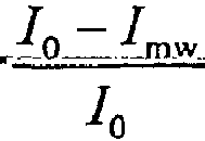

- The lower two panels show the measured distribution of

cell 1 delimiting saidcell 1. - A question that arises is how imaging microwave fields with near room-temperature atoms compares to using ultracold atoms. Using thermal instead of ultracold atoms as in [Boehi10] has the following consequences: First, thermal atoms move much faster than ultracold atoms (for rubidium, the mean thermal velocity at 300 K, is


- There are ways to relax both restrictions: One way to 'effectively' slow down the atoms is using a heavy, noble buffer gas like neon, argon, krypton or xenon [Franzen59] to change the Rb motion from the ballistic to the diffusive regime. Neon is particularly well suited since the cross section for collisional depolarization between Rb and Ne is very small (5.2×10⁻²³cm2 [Franzen59]). Using e.g. 10 mbar of neon buffer gas, the rubidium atoms diffuse a distance of ∼430 µm in 30 µs [Franzen59], which has to be compared with 9 mm of ballistic motion for the case without buffer gas. The presence of buffer gas does not only improve the spatial resolution but also enhances the microwave field sensitivity. Even for small buffer gas pressures, the mean free path length l mfp for a Rb atom gets much smaller than the microwave wavelength λ mw. Thus, we enter the regime of Dicke narrowing [Frueholz85] where the microwave Doppler shifts seen by the atoms during their diffusive motion effectively cancel, such that the microwave resonances ωi can be as narrow as 20 Hz [Frueholz85]. A slight drawback of this slowing down is that the presence of buffer gas leads to line shifts and broadening of the optical [Rotondaro97] and line shifts of the microwave transition frequencies ωi [Bean75, Oreto04]. Furthermore, the absorption of the Rb vapor decreases [Rotondaro97]: with 10 mbar Ne buffer gas and I/I sat=0.1 we measure an optical density of the Rb vapor of 0.5 after dt Pump. Without buffer gas and I/I sat∼0.1 (I/I sat∼0.01), we measure an optical density of 4.2 (5.4).
- It has been observed before that the presence of Ne buffer gas leads to a decrease of the atomic absorption [Rotondaro97], but the drop in absorption measured in our example is much higher than reported in ref. [Rotondaro97]. The reason for this is not fully understood, but the lowered absorption enhances the signal seen by our camera, while at the same time benefiting from increased spatial resolution due to the buffer gas. A higher absorption allows the construction of thinner devices. Furthermore, the laser absorption can be adjusted very well via the Rb vapor pressure, which in turn has a strong dependence on the cell temperature. The pump laser polarization is circular, but it turned out only to be of significance for quantization fields B 0 pointing along the laser direction with B0 ≥ 10G.
- Another possibility to simultaneously get good spatial and microwave sensitivity with thermal atoms would be to confine the atoms in an array of micromachined cells, e.g. fabricated into a glass substrate, similar to references [Baluktsian10, Liew04]. Normally, the rubidium atom's hyperfine state is lost after one collision with the confining glass wall [Franzen59, Sargsyan11]. Using recently developed alkene coatings as in [Balabas10a], the atom's hyperfine state survives up to 106 atom-wall collisions without change, increasing the maximum interaction time dt mw for a given resolution by a
factor 106 as compared to the case without micromachined cells and without buffer gas. This increases the microwave sensitivity by the same factor. Since the length of such a miniature cell would typically be some µm, and therefore much less than λ mw, also in this situation we benefit from Dicke narrowing [Frueholz85]. The Dicke narrowing in a coated cell can be even more efficient than using buffer gas since the atoms have a high probability of being reflected from a cell wall with the same velocity but in opposite direction, which leads to very good cancelation of the Doppler shift. This way, clearly resolvable Rabi oscillations whose frequency is equal to a Dicke-narrowed linewidth of 20 Hz are achievable [Frueholz85]. Such a Rabi frequency is caused by a microwave magnetic field amplitude of only Bi ∼ 10-5 G. The only drawback of coated cells is that the temperature tuning range of the cells and therefore the tuning range of the vapor pressure becomes limited [Balabas10], because melting of the coating has to be avoided. - A small amount of Rb (or other alkali atoms) could be deposited in each microcell during fabrication. The Rb vapor density could then be controlled by temperature or by light-induced desorption as in [Ghosh06]. Alternatively, the different microcells could be connected by thin trenches in the substrate to allow atoms to be introduced into such a system from a single reservoir as in the present example. It is also possible to effectively slow down the atoms by using micromachined holes filled with buffer gas [Liew04].
- We now estimate the microwave field sensitivity that can be obtained with such microcells. Assuming a photon-shot-noise-limited imaging system and


- The method and device according to the invention presented here is not restricted to fixed frequencies. Instead, the transition frequencies ωi can be tuned via the static magnetic field B0 . Using magnetic fields of up to 1.6 T, which is the saturation magnetic field of neodymium magnets, the transition frequencies can be tuned to up to 50 GHz for 87Rb, see
Figure 4 showing the hyperfine levels of 87Rb as a function of static magnetic field B0 . For large B0 , transition frequencies in the range of several tens of GHz are accessible. With magnetic fields B0>1000 G, we start entering the Paschen-Back regime, where the matrix elements of Eqns. [1-5] change. Nevertheless, a full reconstruction of the microwave field is possible. At the low-frequency end, the zero-field hyperfine splitting sets a limit on the microwave transition frequencies. Atoms with smaller hyperfine splitting such as 85Rb (3.0 GHz) or 39K (0.5 GHz) allow one to access the regime of low frequencies. - Furthermore, readout does not necessarily have to rely on absorption imaging, but could equally well be done using fluorescence imaging [Ketterle99].
- The simplicity of the present method allows for the construction of integrated microwave field imaging devices. Preferably, such a device consists of micromachined cells [Baluktsian10] and integrated electro magnets to tune the transition frequencies to the desired values.
-
- [Sayil05] S. Sayil, D.V. Kerns, and S.E. Kerns. A survey of contactless measurement and testing techniques. Potentials, IEEE, 24:25-28, 2005.
- [Boehi10] P. Böhi, M. F. Riedel, T. W. Hänsch, and P. Treutlein. Imaging of microwave felds using ultracold atoms. Appl. Phys. Lett., 97:051101, 2010.
- [BoehiThesis10] P. Böhi. Coherent manipulation of ultracold atoms with microwave near-fields. PhD thesis, Ludwig-Maximilians-Universität München and Max-Planck-Institut für Quantenoptik, 2010. published as MPQ report 333.
- [Farkas09] D. M. Farkas, K. M. Hudek, E. A. Salim, S. R. Segal, M. B. Squires, and D. Z. Anderson. A compact, transportable, microchip-based system for high repetition rate production of bose-einstein condensates. Appl. Phys. Lett., 96:093102, 2010.
- [Haensch05] T. Hänsch, J. Alnis. P. Fendel, M. Fischer, C. Gohle, M. Herrmann, R. Holzwarth, N. Kolachevsky, T. Udem, and M. Zimmermann. Precision spectroscopy of hydrogen and femtosecond laser frequency combs. Phil. Trans. R. Soc. A, 363:2155, 2005.
- [Danielli00] A. Danielli, P. Rusian, A. Arie, M. Chou, and M. Fejer. Frequency stabilization of a frequency-doubled 1556-nm source to the 5S1/2 → 5D5/2 two-photon transitions of rubidium. Opt. Lett., 25(12):905, 2000.
- [Budker07] D Budker and M. Romalis Optical magnetometry Nature Physics, 3:227, 2007.
- [Gentile89] T.R. Gentile, B.J. Hughey, D. Kleppner, and T.W. Ducas. Experimental study of one- and two-photon rabi oscillations. Phys. Rev. A, 40:5103, 1989.
- [Ketterle99] W. Ketterle, D.S. Durfee, and D.M. Stamper-Kurn. Making, probing and understanding Bose-Einstein condensates. In M. Inguscio, S. Stringari, and C.E. Wieman, editors, Bose-Einstein condensation in atomic gases, Proceedings of the International School of Physics "Enrico Fermi », Course CXL, pages 67-176, Amsterdam, 1999.
- [Franzen59] W. Franzen. Spin relaxation of optically aligned rubidium vapor. Phys. Rev. Lett., 115(4):850-858, 1959.
- [Boehi09] P. Böhi, M. F. Riedel, J. Hoffrogge, J. Reichel, T. W. Hänsch, and P. Treutlein. Coherent manipulation of bose-einstein condensates with state-dependent microwave potentials on an atom chip. Nature Phys., 5:592-597, 2009.
- [Frueholz85] R. Frueholz and C. Volk. Analysis of dicke narrowing in wall-coated and buffer-gas-filled atomic storage cells. J. Phys. B: At. Mol. Opt. Phys., 18:4055-4067, 1985.
- [Rotondaro97] M. D. Rotondaro and G. P. Perram. Collisional broadening and shift of the rubidium D1 and D2 lines (52S1/2 →52P1/2, 52P3/2) by rare gases, H2, D2, N2, CH4 and CF4. J. Quant. Spectrosc. Radiat. Transfer, 57:497-507, 1997.
- [Bean75] B. L. Bean and R. H. Lambert. Temperature dependence of hyperfine density shifts. iii. 23Na, 39K, and 85Rb in He, Ne, Ar, and N2. Phys. Rev. A, 12(4):1498, 1975.
- [Oreto] P. J. Oreto, Y.-Y. Jau, A. B. Post, N. N. Kuzma, and W. Happer. Buffer-gas-induced shift and broadening of hyperfine resonances in alkali-metal vapors. Phys. Rev. A, 69:042716, 2004.
- [Siddons08] P. Siddons, C. Adams, C. Ge, and I. Hughes. Absolute absorption on rubidium D lines: Comparison between theory and experiment. J. Phys. B: At. Mol. Opt. Phys., 41:155004, 2008.
- [Baluktsian10] T. Baluktsian, C. Urban, T. Bublat, H. Giessen, R. Löw, and T. Pfau. Fabrication method for microscopic vapour cells for alkali atoms. Opt. Lett., 35(12):1950, 2010.
- [Liew04] L. Liew, S. Knappe, J. Moreland, H. Robinson, L. Hollberg, and J. Kitching. Microfabricated alkali atom vapour cells. Appl. Phys. Lett., 84(14):2694, 2004.
- [Sargsyan07] A. Sargsyan, C. Leroy, Y. Pashayan-Leroy, R. Mirzoyan, A. Papoyan, and D. Sarkisyan. High contrast D1 line electromagnetically induced transparency in nanometric-thin rubidium vapor cell. preprint arXiv:1102.3824 [atom-ph], 2007.
- [Balabas10] M. Balabas, T. Karaulanov, M. Ledbetter, and D. Budker. Polarized alkali-metal vapor with minute-long transverse spin-relaxation time. Phys. Rev. Lett., 105:070801, 2010.
- [Gosh06] S. Ghosh, A. Bhagwat, C. Renshaw, S. Goh, and A. Gaeta. Low-light-level optical interactions with rubidium vapor in a photonic band-gap fiber. Phys. Rev. Lett., 97:2006, 2006.
- the following documents have been cited during the patent examination procedure:
-
US 2011/234219 A1 (BOEHI PASCAL [DE] ET AL HAENSCH THEODOR W [DE] ET AL) 29 September 2011 (2011-09-29), where a similar method is applied to ultra-cold atoms of a Bose-Einstein condensate, - BÜCKER R ET AL: "Single-particle-sensitive imaging of freely propagating ultracold atoms", NEW JOURNAL OF PHYSICS, INSTITUTE OF PHYSICS PUBLISHING, BRISTOL, GB, vol. 11, no. 10, 1 October 2009 (2009-10-01), page 103039, XP020165420,ISSN: 1367-2630, DOI: 10.1088/1367-2630/11/10/103039,
-
US 7 002 174 B2 (IL ICHEV EVGENI [DE] ET AL) 21 February 2006 (2006-02-21)
Claims (15)
- Device for imaging a microwave magnetic field polarization component (B-, Bπ, B +) of a microwave relative to a static magnetic field (B0 ), comprising:- a preparation means being designed to prepare an atomic vapor (10) comprising a plurality of thermal atoms having a temperature between 10°C and 300°C in a first hyperfine state, particularly a dark state to applied laser light, which first hyperfine state is energetically split from other hyperfine states due to the zero-field hyperfine splitting and/or due to a static magnetic field (B0 ) generated by said preparation means, such that said microwave whose magnetic field polarization component (B- , Bπ, B +) is to be imaged is able to drive Rabi oscillations of said plurality of thermal atoms between said first hyperfine state and a second hyperfine state with a Rabi frequency (Ω i (r)) that is proportional to said magnetic field polarization component (B- , Bπ, B+ ),- at least one cell (1) enclosing said plurality of thermal atoms (10), and- an imaging means being designed to capture a state image in at least one of the hyperfine states of said plurality of atoms representing the spatial atomic density distribution (Ne ) being a function of the Rabi frequency (Ω i (r)) of said Rabi oscillations,characterized in that
said plurality of thermal atoms has a temperature between 10°C and 300°C, wherein the device comprises a heating means for heating said plurality of atoms residing in the at least one cell (1). - Device according to claim 1, characterized in that the device further comprises a microwave generating device for generating said microwave comprising said magnetic field polarization component (B- , Bπ , B +) to be imaged.
- Device according to claim 1 or 2, characterized in that the device comprises a controlling means being adapted to activate a microwave generating device for generating said microwave for a pre-defined duration (dtmw ) so that said microwave generated by the microwave generating device is a microwave pulse.
- Device according to one of the preceding claims, characterized in that the plurality of thermal atoms is formed by alkali atoms, particularly 87Rb.
- Device according to one of the preceding claims, characterized in that the preparation means comprises a laser (20) being adapted to illuminate said plurality of thermal atoms so as to accumulate them in said first hyperfine state, wherein particularly in case said plurality of thermal atoms is formed by 87Rb atoms said laser (20) is adapted to illuminate the 87Rb atoms with laser light (2) having a wavelength being resonant with the D2 transition from 52S1/2 F=2 to 52P3/2 F'=1 or 2 of 87Rb such that the excited 87Rb atoms consequently decay into the first hyperfine state F=1.
- Device according to claims 3 and 5, characterized in that the controlling means is designed to switch on the laser (20) for a first optical pumping period during which the microwave generating device (3) is switched off or during which said microwave is not present, wherein particularly said first optical pumping period (dtpump ) has a duration in the range of 100 µs to 10s, in particular 100 ms.
- Device according to one of the preceding claims, characterized in that the imaging means is designed to capture an absorption image or a fluorescence image as said state image, wherein the imaging means particularly comprises said laser (20) being adapted to shine a laser pulse (2) of a pre-defined duration (dtimg ), particularly 10 µs, on the plurality of thermal atoms resonant with a transition from the second hyperfine state to an excited state, wherein particularly in case said plurality of thermal atoms is formed by 87Rb atoms said laser (20) is adapted to shine a laser pulse (2) of said pre-defined duration (dtimg ) being resonant with the transition of 87Rb from 52S1/2 F=2 to 52P3/2 F'=3, wherein particularly the imaging means further comprises a camera (6) for imaging the shadow cast by the resonant atoms excited by said laser pulse (2) or the fluorescence of the resonant atoms excited by said laser pulse (2), and wherein particularly the controlling means is adapted to activate the laser (20) for generating said laser pulse (2) for said pre-defined duration (dtimg ).
- Device according to one of the preceding claims, characterized in that the device comprises a support for retaining the microwave generating device and/or for retaining a microwave device (3) coupled to the microwave generating device or comprised by the microwave generating device, so that said microwave device (3) exhibits said microwave comprising said magnetic field polarization component (B- , B π , B +) to be imaged when the microwave generating device is activated, wherein particularly the microwave device (3) is designed to be interchangeable with another microwave device, and wherein particularly the microwave device (3) is a coplanar wave guide.
- Device according to claim 8, characterized in that the support is designed to rotate the microwave generating device and/or the microwave device (3).
- Device according to one of the preceding claims, characterized in that the device comprises the heating means for heating said plurality of atoms residing in the at least one cell (1) so as to adjust the pressure of the atomic vapor formed by the plurality of atoms, wherein the heating means is particularly designed to adjust the temperature of the cell in the range of 30°C to 300°C, wherein particularly the heating means is formed as an oven enclosing the at least one cell (1).
- Device according to one of the preceding claims, characterized in that the at least one cell (1) is connected to a buffer gas reservoir (51) containing buffer gas atoms for forming a buffer gas enclosed by the cell (1) and/or in that atoms for forming a buffer gas are deposited in the at least one cell (1), particularly in a second recess of the at least one cell (1), wherein said atoms for forming a buffer gas are noble gas atoms, particularly Ne.
- Device according to one of the preceding claims, characterized in that an inside of the at least one cell (1) facing an inner space enclosed by the at least one cell (1) comprises a coating, particularly an alkene coating, such that the probability that a hyperfine state of an atom of the atomic vapor (10) survives upon a collision of the atom with the cell is increased compared to having no coating of said inside.
- Device according to one of the preceding claims, characterized in that the device comprises a plurality of cells forming an array, particularly a micromachined array of cells, wherein the plurality of cells is particularly formed into a substrate, particularly a glass or a quartz substrate.
- Device according to claim 13, characterized in that the cells are connected by conduits so as to allow for introducing atoms for forming the atomic vapor (10) into the cells from a single atomic reservoir and/or so as to allow for introducing buffer gas atoms, particularly noble gas atoms, particularly Ne, into the cells from a single buffer gas reservoir.
- Method for sensing a microwave magnetic field polarization component (B- , Bπ, B +) of a microwave relative to a static magnetic field B0 , comprising the steps of:- generating a static magnetic field B0 having a predetermined direction and strength B0,- preparing an atomic vapor comprising a plurality of thermal atoms having a temperature between 10°C and 300°C in a pre-defined first hyperfine state, particularly a dark state to applied laser light, in a static magnetic field such that the first hyperfine state is energetically split from at least one other hyperfine state,- generating a microwave comprising said magnetic field polarization component (B- , Bπ, B +) to be sensed so that the microwave drives Rabi oscillations of said plurality of thermal atoms between said first hyperfine state and a second hyperfine state, which Rabi oscillations are proportional to said magnetic field polarization component (B- , Bπ , B+ ), and- capturing a state image of said plurality of atoms representing the spatial atomic density distribution (Ne ) being a function of the Rabi frequency (Ω i (r)) of said Rabi oscillations, characterized in that the thermal atoms (10) have a temperature between 10°C and 300°C.
Priority Applications (1)
| Application Number | Priority Date | Filing Date | Title |
|---|---|---|---|
| EP13717444.7A EP2828676B1 (en) | 2012-03-23 | 2013-03-23 | Simple microwave field imaging device |
Applications Claiming Priority (3)
| Application Number | Priority Date | Filing Date | Title |
|---|---|---|---|
| EP12161027 | 2012-03-23 | ||
| PCT/EP2013/056172 WO2013139989A1 (en) | 2012-03-23 | 2013-03-23 | Simple microwave field imaging device |
| EP13717444.7A EP2828676B1 (en) | 2012-03-23 | 2013-03-23 | Simple microwave field imaging device |
Publications (2)
| Publication Number | Publication Date |
|---|---|
| EP2828676A1 EP2828676A1 (en) | 2015-01-28 |
| EP2828676B1 true EP2828676B1 (en) | 2018-01-10 |
Family
ID=48142731
Family Applications (1)
| Application Number | Title | Priority Date | Filing Date |
|---|---|---|---|
| EP13717444.7A Active EP2828676B1 (en) | 2012-03-23 | 2013-03-23 | Simple microwave field imaging device |
Country Status (3)
| Country | Link |
|---|---|
| US (1) | US9971000B2 (en) |
| EP (1) | EP2828676B1 (en) |
| WO (1) | WO2013139989A1 (en) |
Families Citing this family (10)
| Publication number | Priority date | Publication date | Assignee | Title |
|---|---|---|---|---|
| KR102362654B1 (en) | 2015-07-03 | 2022-02-15 | 삼성전자주식회사 | Oven |
| CN106405622B (en) * | 2016-08-30 | 2019-04-05 | 中国科学院合肥物质科学研究院 | A fast nuclear cross-section Doppler broadening method |
| GB2577727B (en) | 2018-10-04 | 2021-07-21 | The Univ Of Durham | Method and apparatus for terahertz or microwave imaging |
| JP7342126B2 (en) * | 2018-12-31 | 2023-09-11 | クオンタム ヴァリー アイデアズ ラボラトリーズ | Electromagnetic field imaging |
| US10989811B2 (en) | 2019-03-29 | 2021-04-27 | Honeywell International Inc. | Image sensing using atomic vapor cell assemblies |
| WO2021188177A1 (en) * | 2020-03-19 | 2021-09-23 | Sri International | Quantum electromagnetic field sensor and imager |
| CN111581860B (en) * | 2020-04-12 | 2023-04-07 | 西安电子科技大学 | Microwave near-field probe spatial resolution analysis method and system and microwave microscope |
| GB2606148B (en) * | 2021-04-26 | 2024-08-28 | Univ Birmingham | High fidelity robust atom optics |
| DE112022002980T5 (en) | 2021-07-06 | 2024-03-28 | Sri International | QUANTUM ELECTROMAGNETIC FIELD SENSOR |
| US12416656B2 (en) * | 2023-07-31 | 2025-09-16 | Rohde & Schwarz Gmbh & Co. Kg | Sensor system and method for analyzing a spectrum of an EM signal |
Family Cites Families (10)
| Publication number | Priority date | Publication date | Assignee | Title |
|---|---|---|---|---|
| US5136261A (en) * | 1990-12-11 | 1992-08-04 | Ball Corporation | Saturated absorption double resonance system and apparatus |
| US5451863A (en) * | 1992-10-30 | 1995-09-19 | International Business Machines Corporation | Fiber optic probe with a magneto-optic film on an end surface for detecting a current in an integrated circuit |
| US7277636B1 (en) * | 2001-01-26 | 2007-10-02 | Gazdzinski Robert F | Optical communication apparatus and methods using pulses having modified propagation speeds |
| US7002174B2 (en) * | 2001-12-18 | 2006-02-21 | D-Wave Systems, Inc. | Characterization and measurement of superconducting structures |
| FR2939884B1 (en) * | 2008-12-16 | 2012-07-27 | Thales Sa | ATOMIC CHIP INTEGRATED MATERIAL WAVE GYROMETER AND ACCELEROMETER |
| US8310230B2 (en) | 2010-03-23 | 2012-11-13 | Max-Planck-Gesellschaft Zur Forderung Der Wissenschaften E.V. | Method and device for sensing microwave magnetic field polarization components |
| WO2014051886A1 (en) * | 2012-08-22 | 2014-04-03 | President And Fellows Of Harvard College | Nanoscale scanning sensors |
| WO2014210486A1 (en) * | 2013-06-28 | 2014-12-31 | Dirk Robert Englund | Wide-field sensing using nitrogen vacancies |
| US10359480B2 (en) * | 2014-02-13 | 2019-07-23 | Presidents And Fellows Of Harvard College | Optically detected magnetic resonance imaging with an electromagnetic field resonator |
| EP3308146B1 (en) * | 2015-06-15 | 2020-02-26 | The Regents of The University of Michigan | Atom-based electromagnetic radiation electric-field sensor |
-
2013
- 2013-03-23 EP EP13717444.7A patent/EP2828676B1/en active Active
- 2013-03-23 WO PCT/EP2013/056172 patent/WO2013139989A1/en not_active Ceased
- 2013-03-23 US US14/387,256 patent/US9971000B2/en active Active
Also Published As
| Publication number | Publication date |
|---|---|
| WO2013139989A1 (en) | 2013-09-26 |
| US9971000B2 (en) | 2018-05-15 |
| EP2828676A1 (en) | 2015-01-28 |
| US20150048824A1 (en) | 2015-02-19 |
Similar Documents
| Publication | Publication Date | Title |
|---|---|---|
| US9971000B2 (en) | Simple microwave field imaging device | |
| Gajdacz et al. | Non-destructive Faraday imaging of dynamically controlled ultracold atoms | |
| Diermaier et al. | In-beam measurement of the hydrogen hyperfine splitting and prospects for antihydrogen spectroscopy | |
| Budker et al. | Optical magnetometry | |
| McGilligan et al. | Grating chips for quantum technologies | |
| Böhi et al. | Simple microwave field imaging technique using hot atomic vapor cells | |
| Malbrunot et al. | The ASACUSA antihydrogen and hydrogen program: results and prospects | |
| US20090289629A1 (en) | Method and Apparatus for Implementing EIT Magnetometry | |
| WO2011117250A1 (en) | Method and device for sensing microwave magnetic field polarization components | |
| Karr et al. | Hydrogen molecular ions: new schemes for metrology and fundamental physics tests | |
| Hassan et al. | Towards single-cell pulsed EPR using VCO-based EPR-on-a-chip detectors | |
| Brazhnikov et al. | Ultrahigh-quality electromagnetically induced absorption resonances in a cesium vapor cell | |
| Jiang et al. | Searches for exotic spin-dependent interactions with spin sensors | |
| WO2009090609A1 (en) | Measurement method using nuclear magnetic resonance spectroscopy and light with orbital angular momentum | |
| Altin et al. | Optically trapped atom interferometry using the clock transition of large 87Rb Bose–Einstein condensates | |
| Geng et al. | Laser-detected magnetic resonance induced by radio-frequency two-photon processes | |
| Babashah et al. | Optically detected magnetic resonance with an open source platform | |
| Svanberg | Laser spectroscopy | |
| Sargsyan et al. | Electromagnetically Induced Transparency and optical pumping processes formed in Cs sub-micron thin cell | |
| Zhang et al. | Picotesla fiberized diamond-based AC magnetometer | |
| Kitching et al. | Atom-based quantum sensing of electromagnetic fields | |
| Guzman et al. | Nonlinear magneto-optical rotation and Zeeman and hyperfine relaxation of potassium atoms in a paraffin-coated cell | |
| Hakhumyan et al. | High-spatial-resolution monitoring of strong magnetic field using Rb vapor nanometric-thin cell | |
| Sautenkov et al. | Quantum defects in Rydberg n D states of optically cooled 7Li atoms | |
| WO2020141536A1 (en) | System and methods for measuring linear and rotational accelerations and magnetic field strengths using individual atoms within an optical lattice formed by lasers |
Legal Events
| Date | Code | Title | Description |
|---|---|---|---|
| PUAI | Public reference made under article 153(3) epc to a published international application that has entered the european phase |
Free format text: ORIGINAL CODE: 0009012 |
|
| 17P | Request for examination filed |
Effective date: 20141023 |
|
| AK | Designated contracting states |
Kind code of ref document: A1 Designated state(s): AL AT BE BG CH CY CZ DE DK EE ES FI FR GB GR HR HU IE IS IT LI LT LU LV MC MK MT NL NO PL PT RO RS SE SI SK SM TR |
|
| AX | Request for extension of the european patent |
Extension state: BA ME |
|
| DAX | Request for extension of the european patent (deleted) | ||
| GRAP | Despatch of communication of intention to grant a patent |
Free format text: ORIGINAL CODE: EPIDOSNIGR1 |
|
| INTG | Intention to grant announced |
Effective date: 20160519 |
|
| GRAJ | Information related to disapproval of communication of intention to grant by the applicant or resumption of examination proceedings by the epo deleted |
Free format text: ORIGINAL CODE: EPIDOSDIGR1 |
|
| INTC | Intention to grant announced (deleted) | ||
| GRAP | Despatch of communication of intention to grant a patent |
Free format text: ORIGINAL CODE: EPIDOSNIGR1 |
|
| INTG | Intention to grant announced |
Effective date: 20170113 |
|
| GRAJ | Information related to disapproval of communication of intention to grant by the applicant or resumption of examination proceedings by the epo deleted |
Free format text: ORIGINAL CODE: EPIDOSDIGR1 |
|
| INTC | Intention to grant announced (deleted) | ||
| GRAP | Despatch of communication of intention to grant a patent |
Free format text: ORIGINAL CODE: EPIDOSNIGR1 |
|
| INTG | Intention to grant announced |
Effective date: 20170717 |
|
| GRAS | Grant fee paid |
Free format text: ORIGINAL CODE: EPIDOSNIGR3 |
|
| GRAA | (expected) grant |
Free format text: ORIGINAL CODE: 0009210 |
|
| AK | Designated contracting states |
Kind code of ref document: B1 Designated state(s): AL AT BE BG CH CY CZ DE DK EE ES FI FR GB GR HR HU IE IS IT LI LT LU LV MC MK MT NL NO PL PT RO RS SE SI SK SM TR |
|
| REG | Reference to a national code |
Ref country code: CH Ref legal event code: EP Ref country code: AT Ref legal event code: REF Ref document number: 962986 Country of ref document: AT Kind code of ref document: T Effective date: 20180115 |
|
| REG | Reference to a national code |
Ref country code: IE Ref legal event code: FG4D |
|
| REG | Reference to a national code |
Ref country code: DE Ref legal event code: R096 Ref document number: 602013031910 Country of ref document: DE |
|
| REG | Reference to a national code |
Ref country code: FR Ref legal event code: PLFP Year of fee payment: 6 |
|
| REG | Reference to a national code |
Ref country code: NL Ref legal event code: MP Effective date: 20180110 |
|
| REG | Reference to a national code |
Ref country code: AT Ref legal event code: MK05 Ref document number: 962986 Country of ref document: AT Kind code of ref document: T Effective date: 20180110 |
|
| PG25 | Lapsed in a contracting state [announced via postgrant information from national office to epo] |
Ref country code: NL Free format text: LAPSE BECAUSE OF FAILURE TO SUBMIT A TRANSLATION OF THE DESCRIPTION OR TO PAY THE FEE WITHIN THE PRESCRIBED TIME-LIMIT Effective date: 20180110 |
|
| PG25 | Lapsed in a contracting state [announced via postgrant information from national office to epo] |
Ref country code: NO Free format text: LAPSE BECAUSE OF FAILURE TO SUBMIT A TRANSLATION OF THE DESCRIPTION OR TO PAY THE FEE WITHIN THE PRESCRIBED TIME-LIMIT Effective date: 20180410 Ref country code: FI Free format text: LAPSE BECAUSE OF FAILURE TO SUBMIT A TRANSLATION OF THE DESCRIPTION OR TO PAY THE FEE WITHIN THE PRESCRIBED TIME-LIMIT Effective date: 20180110 Ref country code: HR Free format text: LAPSE BECAUSE OF FAILURE TO SUBMIT A TRANSLATION OF THE DESCRIPTION OR TO PAY THE FEE WITHIN THE PRESCRIBED TIME-LIMIT Effective date: 20180110 Ref country code: LT Free format text: LAPSE BECAUSE OF FAILURE TO SUBMIT A TRANSLATION OF THE DESCRIPTION OR TO PAY THE FEE WITHIN THE PRESCRIBED TIME-LIMIT Effective date: 20180110 Ref country code: ES Free format text: LAPSE BECAUSE OF FAILURE TO SUBMIT A TRANSLATION OF THE DESCRIPTION OR TO PAY THE FEE WITHIN THE PRESCRIBED TIME-LIMIT Effective date: 20180110 Ref country code: CY Free format text: LAPSE BECAUSE OF FAILURE TO SUBMIT A TRANSLATION OF THE DESCRIPTION OR TO PAY THE FEE WITHIN THE PRESCRIBED TIME-LIMIT Effective date: 20180110 |
|
| PG25 | Lapsed in a contracting state [announced via postgrant information from national office to epo] |
Ref country code: BG Free format text: LAPSE BECAUSE OF FAILURE TO SUBMIT A TRANSLATION OF THE DESCRIPTION OR TO PAY THE FEE WITHIN THE PRESCRIBED TIME-LIMIT Effective date: 20180410 Ref country code: GR Free format text: LAPSE BECAUSE OF FAILURE TO SUBMIT A TRANSLATION OF THE DESCRIPTION OR TO PAY THE FEE WITHIN THE PRESCRIBED TIME-LIMIT Effective date: 20180411 Ref country code: SE Free format text: LAPSE BECAUSE OF FAILURE TO SUBMIT A TRANSLATION OF THE DESCRIPTION OR TO PAY THE FEE WITHIN THE PRESCRIBED TIME-LIMIT Effective date: 20180110 Ref country code: IS Free format text: LAPSE BECAUSE OF FAILURE TO SUBMIT A TRANSLATION OF THE DESCRIPTION OR TO PAY THE FEE WITHIN THE PRESCRIBED TIME-LIMIT Effective date: 20180510 Ref country code: LV Free format text: LAPSE BECAUSE OF FAILURE TO SUBMIT A TRANSLATION OF THE DESCRIPTION OR TO PAY THE FEE WITHIN THE PRESCRIBED TIME-LIMIT Effective date: 20180110 Ref country code: AT Free format text: LAPSE BECAUSE OF FAILURE TO SUBMIT A TRANSLATION OF THE DESCRIPTION OR TO PAY THE FEE WITHIN THE PRESCRIBED TIME-LIMIT Effective date: 20180110 Ref country code: RS Free format text: LAPSE BECAUSE OF FAILURE TO SUBMIT A TRANSLATION OF THE DESCRIPTION OR TO PAY THE FEE WITHIN THE PRESCRIBED TIME-LIMIT Effective date: 20180110 Ref country code: PL Free format text: LAPSE BECAUSE OF FAILURE TO SUBMIT A TRANSLATION OF THE DESCRIPTION OR TO PAY THE FEE WITHIN THE PRESCRIBED TIME-LIMIT Effective date: 20180110 |
|
| REG | Reference to a national code |
Ref country code: DE Ref legal event code: R097 Ref document number: 602013031910 Country of ref document: DE |
|
| PG25 | Lapsed in a contracting state [announced via postgrant information from national office to epo] |
Ref country code: EE Free format text: LAPSE BECAUSE OF FAILURE TO SUBMIT A TRANSLATION OF THE DESCRIPTION OR TO PAY THE FEE WITHIN THE PRESCRIBED TIME-LIMIT Effective date: 20180110 Ref country code: IT Free format text: LAPSE BECAUSE OF FAILURE TO SUBMIT A TRANSLATION OF THE DESCRIPTION OR TO PAY THE FEE WITHIN THE PRESCRIBED TIME-LIMIT Effective date: 20180110 Ref country code: AL Free format text: LAPSE BECAUSE OF FAILURE TO SUBMIT A TRANSLATION OF THE DESCRIPTION OR TO PAY THE FEE WITHIN THE PRESCRIBED TIME-LIMIT Effective date: 20180110 Ref country code: RO Free format text: LAPSE BECAUSE OF FAILURE TO SUBMIT A TRANSLATION OF THE DESCRIPTION OR TO PAY THE FEE WITHIN THE PRESCRIBED TIME-LIMIT Effective date: 20180110 |
|
| PLBE | No opposition filed within time limit |
Free format text: ORIGINAL CODE: 0009261 |
|
| STAA | Information on the status of an ep patent application or granted ep patent |
Free format text: STATUS: NO OPPOSITION FILED WITHIN TIME LIMIT |
|
| PG25 | Lapsed in a contracting state [announced via postgrant information from national office to epo] |
Ref country code: MC Free format text: LAPSE BECAUSE OF FAILURE TO SUBMIT A TRANSLATION OF THE DESCRIPTION OR TO PAY THE FEE WITHIN THE PRESCRIBED TIME-LIMIT Effective date: 20180110 Ref country code: CZ Free format text: LAPSE BECAUSE OF FAILURE TO SUBMIT A TRANSLATION OF THE DESCRIPTION OR TO PAY THE FEE WITHIN THE PRESCRIBED TIME-LIMIT Effective date: 20180110 Ref country code: SK Free format text: LAPSE BECAUSE OF FAILURE TO SUBMIT A TRANSLATION OF THE DESCRIPTION OR TO PAY THE FEE WITHIN THE PRESCRIBED TIME-LIMIT Effective date: 20180110 Ref country code: DK Free format text: LAPSE BECAUSE OF FAILURE TO SUBMIT A TRANSLATION OF THE DESCRIPTION OR TO PAY THE FEE WITHIN THE PRESCRIBED TIME-LIMIT Effective date: 20180110 Ref country code: SM Free format text: LAPSE BECAUSE OF FAILURE TO SUBMIT A TRANSLATION OF THE DESCRIPTION OR TO PAY THE FEE WITHIN THE PRESCRIBED TIME-LIMIT Effective date: 20180110 |
|
| REG | Reference to a national code |
Ref country code: BE Ref legal event code: MM Effective date: 20180331 |
|
| 26N | No opposition filed |
Effective date: 20181011 |
|
| REG | Reference to a national code |
Ref country code: IE Ref legal event code: MM4A |
|
| PG25 | Lapsed in a contracting state [announced via postgrant information from national office to epo] |
Ref country code: LU Free format text: LAPSE BECAUSE OF NON-PAYMENT OF DUE FEES Effective date: 20180323 |
|
| PG25 | Lapsed in a contracting state [announced via postgrant information from national office to epo] |
Ref country code: IE Free format text: LAPSE BECAUSE OF NON-PAYMENT OF DUE FEES Effective date: 20180323 |
|
| PG25 | Lapsed in a contracting state [announced via postgrant information from national office to epo] |
Ref country code: BE Free format text: LAPSE BECAUSE OF NON-PAYMENT OF DUE FEES Effective date: 20180331 Ref country code: SI Free format text: LAPSE BECAUSE OF FAILURE TO SUBMIT A TRANSLATION OF THE DESCRIPTION OR TO PAY THE FEE WITHIN THE PRESCRIBED TIME-LIMIT Effective date: 20180110 |
|
| PG25 | Lapsed in a contracting state [announced via postgrant information from national office to epo] |
Ref country code: MT Free format text: LAPSE BECAUSE OF NON-PAYMENT OF DUE FEES Effective date: 20180323 |
|
| PG25 | Lapsed in a contracting state [announced via postgrant information from national office to epo] |
Ref country code: TR Free format text: LAPSE BECAUSE OF FAILURE TO SUBMIT A TRANSLATION OF THE DESCRIPTION OR TO PAY THE FEE WITHIN THE PRESCRIBED TIME-LIMIT Effective date: 20180110 |
|
| PG25 | Lapsed in a contracting state [announced via postgrant information from national office to epo] |
Ref country code: PT Free format text: LAPSE BECAUSE OF FAILURE TO SUBMIT A TRANSLATION OF THE DESCRIPTION OR TO PAY THE FEE WITHIN THE PRESCRIBED TIME-LIMIT Effective date: 20180110 Ref country code: HU Free format text: LAPSE BECAUSE OF FAILURE TO SUBMIT A TRANSLATION OF THE DESCRIPTION OR TO PAY THE FEE WITHIN THE PRESCRIBED TIME-LIMIT; INVALID AB INITIO Effective date: 20130323 |
|
| PG25 | Lapsed in a contracting state [announced via postgrant information from national office to epo] |
Ref country code: MK Free format text: LAPSE BECAUSE OF NON-PAYMENT OF DUE FEES Effective date: 20180110 |
|
| P01 | Opt-out of the competence of the unified patent court (upc) registered |
Effective date: 20230526 |
|
| PGFP | Annual fee paid to national office [announced via postgrant information from national office to epo] |
Ref country code: CH Payment date: 20250401 Year of fee payment: 13 |
|
| REG | Reference to a national code |
Ref country code: CH Ref legal event code: U11 Free format text: ST27 STATUS EVENT CODE: U-0-0-U10-U11 (AS PROVIDED BY THE NATIONAL OFFICE) Effective date: 20260401 |
|
| PGFP | Annual fee paid to national office [announced via postgrant information from national office to epo] |
Ref country code: GB Payment date: 20260324 Year of fee payment: 14 |
|
| PGFP | Annual fee paid to national office [announced via postgrant information from national office to epo] |
Ref country code: DE Payment date: 20260320 Year of fee payment: 14 |
|
| PGFP | Annual fee paid to national office [announced via postgrant information from national office to epo] |
Ref country code: FR Payment date: 20260324 Year of fee payment: 14 |