EP2826837A1 - Organic light emitting device - Google Patents
Organic light emitting device Download PDFInfo
- Publication number
- EP2826837A1 EP2826837A1 EP14177131.1A EP14177131A EP2826837A1 EP 2826837 A1 EP2826837 A1 EP 2826837A1 EP 14177131 A EP14177131 A EP 14177131A EP 2826837 A1 EP2826837 A1 EP 2826837A1
- Authority
- EP
- European Patent Office
- Prior art keywords
- group
- light emitting
- organic light
- emitting device
- chemical formula
- Prior art date
- Legal status (The legal status is an assumption and is not a legal conclusion. Google has not performed a legal analysis and makes no representation as to the accuracy of the status listed.)
- Granted
Links
- 0 **(*)*[n]1c2ccccc2c2c1cccc2 Chemical compound **(*)*[n]1c2ccccc2c2c1cccc2 0.000 description 2
- QWNIZJPCZMJAFW-UHFFFAOYSA-N C1C=CC=CC1c1c(cccc2)c2nc(-[n]2c(ccc(-c(cc3)cc(c4ccccc44)c3[n]4-c3ccccc3)c3)c3c3c2cccc3)n1 Chemical compound C1C=CC=CC1c1c(cccc2)c2nc(-[n]2c(ccc(-c(cc3)cc(c4ccccc44)c3[n]4-c3ccccc3)c3)c3c3c2cccc3)n1 QWNIZJPCZMJAFW-UHFFFAOYSA-N 0.000 description 1
- WZAKMOUIQWRNOI-UHFFFAOYSA-N c(cc1)ccc1-c(cc1)ccc1-c1c(cccc2)c2nc(-[n]2c(ccc(-c(cc3c4ccccc44)ccc3[n]4-c3ccccc3)c3)c3c3c2cccc3)n1 Chemical compound c(cc1)ccc1-c(cc1)ccc1-c1c(cccc2)c2nc(-[n]2c(ccc(-c(cc3c4ccccc44)ccc3[n]4-c3ccccc3)c3)c3c3c2cccc3)n1 WZAKMOUIQWRNOI-UHFFFAOYSA-N 0.000 description 1
Images


Classifications
-
- H—ELECTRICITY
- H10—SEMICONDUCTOR DEVICES; ELECTRIC SOLID-STATE DEVICES NOT OTHERWISE PROVIDED FOR
- H10K—ORGANIC ELECTRIC SOLID-STATE DEVICES
- H10K85/00—Organic materials used in the body or electrodes of devices covered by this subclass
- H10K85/60—Organic compounds having low molecular weight
- H10K85/649—Aromatic compounds comprising a hetero atom
- H10K85/657—Polycyclic condensed heteroaromatic hydrocarbons
- H10K85/6572—Polycyclic condensed heteroaromatic hydrocarbons comprising only nitrogen in the heteroaromatic polycondensed ring system, e.g. phenanthroline or carbazole
-
- H—ELECTRICITY
- H10—SEMICONDUCTOR DEVICES; ELECTRIC SOLID-STATE DEVICES NOT OTHERWISE PROVIDED FOR
- H10K—ORGANIC ELECTRIC SOLID-STATE DEVICES
- H10K50/00—Organic light-emitting devices
- H10K50/10—OLEDs or polymer light-emitting diodes [PLED]
- H10K50/11—OLEDs or polymer light-emitting diodes [PLED] characterised by the electroluminescent [EL] layers
-
- C—CHEMISTRY; METALLURGY
- C09—DYES; PAINTS; POLISHES; NATURAL RESINS; ADHESIVES; COMPOSITIONS NOT OTHERWISE PROVIDED FOR; APPLICATIONS OF MATERIALS NOT OTHERWISE PROVIDED FOR
- C09K—MATERIALS FOR MISCELLANEOUS APPLICATIONS, NOT PROVIDED FOR ELSEWHERE
- C09K11/00—Luminescent materials, e.g. electroluminescent or chemiluminescent
- C09K11/06—Luminescent materials, e.g. electroluminescent or chemiluminescent containing organic luminescent materials
-
- H—ELECTRICITY
- H05—ELECTRIC TECHNIQUES NOT OTHERWISE PROVIDED FOR
- H05B—ELECTRIC HEATING; ELECTRIC LIGHT SOURCES NOT OTHERWISE PROVIDED FOR; CIRCUIT ARRANGEMENTS FOR ELECTRIC LIGHT SOURCES, IN GENERAL
- H05B33/00—Electroluminescent light sources
- H05B33/10—Apparatus or processes specially adapted to the manufacture of electroluminescent light sources
-
- H—ELECTRICITY
- H10—SEMICONDUCTOR DEVICES; ELECTRIC SOLID-STATE DEVICES NOT OTHERWISE PROVIDED FOR
- H10K—ORGANIC ELECTRIC SOLID-STATE DEVICES
- H10K50/00—Organic light-emitting devices
- H10K50/10—OLEDs or polymer light-emitting diodes [PLED]
- H10K50/14—Carrier transporting layers
- H10K50/15—Hole transporting layers
-
- C—CHEMISTRY; METALLURGY
- C09—DYES; PAINTS; POLISHES; NATURAL RESINS; ADHESIVES; COMPOSITIONS NOT OTHERWISE PROVIDED FOR; APPLICATIONS OF MATERIALS NOT OTHERWISE PROVIDED FOR
- C09K—MATERIALS FOR MISCELLANEOUS APPLICATIONS, NOT PROVIDED FOR ELSEWHERE
- C09K2211/00—Chemical nature of organic luminescent or tenebrescent compounds
- C09K2211/10—Non-macromolecular compounds
- C09K2211/1003—Carbocyclic compounds
- C09K2211/1007—Non-condensed systems
-
- C—CHEMISTRY; METALLURGY
- C09—DYES; PAINTS; POLISHES; NATURAL RESINS; ADHESIVES; COMPOSITIONS NOT OTHERWISE PROVIDED FOR; APPLICATIONS OF MATERIALS NOT OTHERWISE PROVIDED FOR
- C09K—MATERIALS FOR MISCELLANEOUS APPLICATIONS, NOT PROVIDED FOR ELSEWHERE
- C09K2211/00—Chemical nature of organic luminescent or tenebrescent compounds
- C09K2211/10—Non-macromolecular compounds
- C09K2211/1003—Carbocyclic compounds
- C09K2211/1011—Condensed systems
-
- C—CHEMISTRY; METALLURGY
- C09—DYES; PAINTS; POLISHES; NATURAL RESINS; ADHESIVES; COMPOSITIONS NOT OTHERWISE PROVIDED FOR; APPLICATIONS OF MATERIALS NOT OTHERWISE PROVIDED FOR
- C09K—MATERIALS FOR MISCELLANEOUS APPLICATIONS, NOT PROVIDED FOR ELSEWHERE
- C09K2211/00—Chemical nature of organic luminescent or tenebrescent compounds
- C09K2211/10—Non-macromolecular compounds
- C09K2211/1003—Carbocyclic compounds
- C09K2211/1014—Carbocyclic compounds bridged by heteroatoms, e.g. N, P, Si or B
-
- C—CHEMISTRY; METALLURGY
- C09—DYES; PAINTS; POLISHES; NATURAL RESINS; ADHESIVES; COMPOSITIONS NOT OTHERWISE PROVIDED FOR; APPLICATIONS OF MATERIALS NOT OTHERWISE PROVIDED FOR
- C09K—MATERIALS FOR MISCELLANEOUS APPLICATIONS, NOT PROVIDED FOR ELSEWHERE
- C09K2211/00—Chemical nature of organic luminescent or tenebrescent compounds
- C09K2211/10—Non-macromolecular compounds
- C09K2211/1018—Heterocyclic compounds
- C09K2211/1025—Heterocyclic compounds characterised by ligands
- C09K2211/1029—Heterocyclic compounds characterised by ligands containing one nitrogen atom as the heteroatom
-
- H—ELECTRICITY
- H10—SEMICONDUCTOR DEVICES; ELECTRIC SOLID-STATE DEVICES NOT OTHERWISE PROVIDED FOR
- H10K—ORGANIC ELECTRIC SOLID-STATE DEVICES
- H10K85/00—Organic materials used in the body or electrodes of devices covered by this subclass
- H10K85/60—Organic compounds having low molecular weight
- H10K85/631—Amine compounds having at least two aryl rest on at least one amine-nitrogen atom, e.g. triphenylamine
- H10K85/633—Amine compounds having at least two aryl rest on at least one amine-nitrogen atom, e.g. triphenylamine comprising polycyclic condensed aromatic hydrocarbons as substituents on the nitrogen atom
-
- H—ELECTRICITY
- H10—SEMICONDUCTOR DEVICES; ELECTRIC SOLID-STATE DEVICES NOT OTHERWISE PROVIDED FOR
- H10K—ORGANIC ELECTRIC SOLID-STATE DEVICES
- H10K85/00—Organic materials used in the body or electrodes of devices covered by this subclass
- H10K85/60—Organic compounds having low molecular weight
- H10K85/631—Amine compounds having at least two aryl rest on at least one amine-nitrogen atom, e.g. triphenylamine
- H10K85/636—Amine compounds having at least two aryl rest on at least one amine-nitrogen atom, e.g. triphenylamine comprising heteroaromatic hydrocarbons as substituents on the nitrogen atom
Definitions
- Embodiments relate to an organic light emitting device.
- cathode ray tubes CRT
- LCD liquid crystal displays
- liquid crystal displays are non-emissive devices that must be provided with a separate backlight to display images, and may have disadvantages of a limited response time and limited viewing angle.
- OLED organic light emitting diode
- the organic light emitting device includes two electrodes facing each other and an organic layer interposed between the two electrodes.
- electrons injected from one electrode and holes injected from another electrode are combined with each other in an emission layer, thereby generating excitons, and energy is outputted from the excitons to thereby emit light.
- the organic light emitting device may be applicable to various fields including a display device and an illumination system.
- Embodiments are directed to an organic light emitting device, including a first electrode and a second electrode facing each other, and an organic layer between the first electrode and the second electrode.
- the organic layer includes an assistance layer on the first electrode and an emission layer on the assistance layer, the assistance layer including a compound represented by Chemical Formula 1:
- n may preferably be 0, and R 1 or R 2 may preferably be condensed to an adjacent substituent or R 1 and R 2 may preferably form a ring.
- the compound represented by Chemical Formula 1 may preferably include at least one selected from the compounds represented by Chemical Formula 1-1 to Chemical Formula 1-9:
- the emission layer may preferably include a host material including a compound represented by Chemical Formula 2:
- the compound represented by Chemical Formula 2 includes at least one selected from the compounds represented by Chemical Formula 2-1 to Chemical Formula 2-6:
- the emission layer may preferably further include a dopant material.
- the dopant material may preferably include a red dopant material, a green dopant material, or a red dopant material.
- the first electrode may preferably be an anode, and the second electrode may preferably be a cathode.
- the organic layer may preferably include a hole injection layer (HIL) between the first electrode and the assistance layer, a hole transport layer (HTL) between the hole injection layer (HIL) and the assistance layer, and an electron transport layer (ETL) between the emission layer and the second electrode.
- HIL hole injection layer
- HTL hole transport layer
- ETL electron transport layer
- substituted refers to a hydrogen atom of a compound substituted with a substituent selected from among halogen atoms (F, Br, Cl, or I), a hydroxyl group, an alkoxy group, a nitro group, a cyano group, an amino group, an azido group, an amidino group, a hydrazino group, a hydrazono group, a carbonyl group, a carbamyl group, a thiol group, an ester group, a carboxyl group or its salt, a sulfonic acid group or its salt, a phosphoric acid or its salt, an alkyl group, a C2-C16 alkenyl group, a C2-C16 alkynyl group, an aryl group, a C7-C13 arylalkyl group, a C1-C4 oxyalkyl group, a C1-C20 heteroalkyl
- hetero refers to containing one to three hetero atoms selected from among N, O, S, and P.
- the thickness and/or relative thickness of the elements may be exaggerated in order to clarify embodiments. Also, the expressions related to positions such as “upper part”, “lower part”, or the like are relatively used for clarification, without limiting absolute positions among the elements.
- FIG. 1 illustrates a view of an organic light emitting device according to an exemplary embodiment.
- an organic light emitting device may include a first electrode 100, a second electrode 300 facing the first electrode 100, and an organic layer 200 interposed between the first electrode 100 and the second electrode 300.
- a substrate may preferably be disposed at the first electrode 100 side or the second electrode 300 side.
- the substrate may preferably include glass, a polymer, or combinations thereof.
- the first electrode 100 may preferably be an anode, and the second electrode 300 may preferably be a cathode.
- the first electrode 100 and the second electrode 300 may preferably be transparent or non-transparent electrodes.
- the first electrode 100 and the second electrode 300 may preferably be a transparent electrode made of ITO (indium tin oxide), IZO (indium zinc oxide), or combinations thereof, or a non-transparent electrode made of aluminum (Al), silver (Ag), magnesium (Mg), or combinations thereof.
- the organic layer 200 may preferably include a hole injection layer (HIL) 210, a hole transport layer (HTL) 220, an assistance layer 230, an emission layer 240, and an electron transport layer (ETL) 250 sequentially disposed on the first electrode 100.
- HIL hole injection layer
- HTL hole transport layer
- ETL electron transport layer
- the hole injection layer (HIL) 210 and the hole transport layer (HTL) 220 may preferably be disposed between the first electrode 100 and the emission layer 240, such that holes may be easily transmitted from the first electrode 100 to the emission layer 240.
- the hole injection layer (HIL) 210 may preferably be formed of a hole injection material.
- the hole injection material may preferably be a phthalocyanine compound such as copper phthalocyanine or the like, m-MTDATA (4,4',4"-tris(3-methylphenylphenylamino)triphenylamine), NPB (N,N'-di(1-naphthyl)-N,N'-diphenylbenzidine), TDATA, 2T-NATA, Pani/DBSA (polyaniline/dodecylbenzene sulfonic acid:polyaniline/dodecylbenzene sulfonic acid), PEDOT/PSS (poly(3,4-ethylene dioxythiophene)/poly(4-styrene sulfonate):poly(3,4-ethylene dioxythiophene)/poly(4-styrene sulfonate)), Pani/CSA (pol
- the hole transport layer (HTL) 220 may preferably contain a hole transport material.
- the hole transport material may preferably be a carbazole derivative such as N-phenylcarbazole, polyvinylcarbazole, or the like, and an amine derivative having an aromatic condensed ring such as NPB, N,N'-bis(3-methylphenyl)-N,N'-diphenyl-[1,1-biphenyl]-4,4'-diamine (TPD), tris(4-carbazoyl-9-ylphenyl)amine (TCTA), or the like.
- a carbazole derivative such as N-phenylcarbazole, polyvinylcarbazole, or the like
- an amine derivative having an aromatic condensed ring such as NPB, N,N'-bis(3-methylphenyl)-N,N'-diphenyl-[1,1-biphenyl]-4,4'-diamine (TPD), tris(
- the assistance layer 230 may preferably be disposed at the hole transport layer (HTL) 220 and the emission layer 240 to adjust a balance of the charges in the organic light emitting device thereby preventing roll-off generation.
- HTL hole transport layer
- the assistance layer 230 may preferably include a compound represented by Chemical Formula 1 below.
- L 1 and L 2 may preferably be independently selected from the group of an amino group, a C1 to C40 alkyl group, a C2 to C40 alkenyl group, a C2 to C40 alkynyl group, , a C5 to C40 aryl group, a C1 to C40 heteroaryl group, a C1 to C40 alkoxy group, a C5 to C40 aryloxy group, a C1 to C40 alkylamino group, a C5 to C40 arylamino group, a C5 to C40 diarylamino group, a C5 to C40 heteroarylamino group, a C2 to C40 diheteroarylamino group, a C6 to C40 arylalkyl group, a C6 to C40 heteroarylalkyl group, a C3 to C40 cycloalkyl group, a C1 to C40 halogenalkyl group, a C3 to C40 heterocyclo
- L 1 and L 2 may be independently selected from the group of a C5 to C40 aryl group, a C1 to C40 heteroaryl group, a C5 to C40 diarylamino group, a C2 to C40 diheteroarylamino group, and a C6 to C40 arylalkyl group, preferably a C5 to C16 aryl group, a C4 to C10 heteroaryl group, a C5 to C15 diarylamino group, a C4 to C10 diheteroarylamino group, and a C6 to C15 arylalkyl group, preferably a C6 to C12 aryl group.
- L 1 and L 2 may be independently selected from the group of phenyl, naphthyl, anthracene and pyrene, more preferably phenyl and naphthyl.
- the above L 1 and L 2 groups are substituted with at least one of the substitute substituents defined above, preferably between 1 and 3 substituents.
- R 1 and R 2 may preferably be independently selected from the group of an amino group, a nitro group, a nitrile group, a C1 to C40 alkyl group, a C2 to C40 alkenyl group, a C2 to C40 alkynyl group, a C5 to C40 aryl group, a C10 to C40 biaryl group, a C1 to C40 heteroaryl group, a C1 to C40 alkoxy group, a C5 to C40 aryloxy group, a C1 to C40 alkylamino group, a C5 to C40 arylamino group, a C5 to C40 diarylamino group, a C5 to C40 heteroarylamino group, a C2 to C40 diheteroarylamino group, a C6 to C40 arylalkyl group, a C6 to C40 heteroarylalkyl group, a C3 to C40 cycloalkyl group, a C6
- R 1 and R 2 may be independently selected from the group of a C5 to C40 aryl group, a C10 to C40 biaryl group, a C1 to C40 heteroaryl group, a C5 to C40 diarylamino group, a C2 to C40 diheteroarylamino group, and a C6 to C40 arylalkyl group, preferably a C5 to C16 aryl group, a C10 to C20 biaryl group, a C4 to C10 heteroaryl group, a C5 to C15 diarylamino group, a C4 to C10 diheteroarylamino group, and a C6 to C15 arylalkyl group, preferably a C6 to C12 aryl group and a C12 to C16 biaryl group.
- R 1 and R 2 may be independently selected from the group of phenyl, naphthyl, anthracene, pyrene and biphenyl, more preferably biphenyl, phenyl and naphthyl.
- R 1 and R 2 may preferably be condensed to the adjacent substituent or may preferably form a ring.
- R 1 and R 2 groups are substituted with at least one of the substitute substituents defined above, preferably between 1 and 3 substituents.
- a compound represented by Chemical Formula 1 may preferably be at least one selected from compounds represented by Chemical Formula 1-1 to Chemical Formula 1-9.
- the compound represented by Chemical Formula 1-1 to Chemical Formula 1-9 may preferably be independently used, at least two or more may preferably be mixed, or at least one may preferably be mixed with a different compound.
- the compound of chemical formula 1 makes up greater than 50% by weight of the assistance layer, preferably greater than 75% by weight, preferably between 85% and 100% of the assistance layer.
- the assistance layer is from 400 ⁇ to 1000 ⁇ , preferably 500 ⁇ to 900 ⁇ , more preferably 600 ⁇ to 800 ⁇ thick.
- the emission layer 240 may preferably be made of a host material and a dopant.
- the dopant may preferably include a material that emits one among primary colors such as red, green, and blue.
- the host material may preferably include a compound represented by Chemical Formula 2.
- R 1 to R 2 may preferably be selected from the group of an amino group, a nitro group, a nitrile group, a C1 to C40 alkyl group, a C2 to C40 alkenyl group, a C2 to C40 alkynyl group, a C5 to C40 aryl group, a C10 to C40 biaryl group, a C1 to C40 heteroaryl group, a C1 to C40 alkoxy group, a C5 to C40 aryloxy group, a C1 to C40 alkylamino group, a C5 to C40 arylamino group, a C5 to C40 diarylamino group, a C5 to C40 heteroarylamino group, a C2 to C40 diheteroarylamino group, a C6 to C40 arylalkyl group, a C6 to C40 heteroarylalkyl group, a C3 to C40 cycloalkyl group, a
- R 3 may preferably be C(H)R 1 where R 1 is as defined above or may preferably form with R 2 a diheteroaryl group with the N atoms that they are bound.
- R 1 to R 3 may preferably be condensed to an adjacent substituent or may preferably form the ring.
- R 1 is selected from the group of a C5 to C40 aryl group, a C10 to C40 biaryl group, a C1 to C40 heteroaryl group, a C5 to C40 diarylamino group, a C2 to C40 diheteroarylamino group, and a C6 to C40 arylalkyl group; preferably a C5 to C16 aryl group, a C10 to C20 biaryl group, a C4 to C10 heteroaryl group, a C5 to C15 diarylamino group, a C4 to C10 diheteroarylamino group, and a C6 to C15 arylalkyl group; preferably a C6 to C12 aryl group and a C12 to C16 biaryl group.
- R 1 is selected from the group of phenyl, naphthyl, anthracene, pyrene and biphenyl, more preferably biphenyl, phenyl and naphthyl.
- R 2 and R 3 form a diheteroaryl group with the N atoms that they are bound to, preferably R 2 and R 3 , the N atoms that they are bound to and the carbon atom linking the N atoms form a substituted or unsubstituted C2 to C40 diheteroaryl group, more preferably a substituted or unsubstituted C3 to C15 diheteroaryl group, more preferably a substituted or unsubstituted C4 to C10 a substituted or unsubstituted.
- R 1 to R 3 groups in Chemical Formula 2 are substituted with at least one of the substitute substituents defined above, preferably between 1 and 3 substituents.
- the ring formed by R 2 and R 3 is substituted with at least one, preferably between 1 and 3 substituents independently selected from the group of a C5 to C40 aryl group, a C10 to C40 biaryl group, a C1 to C40 heteroaryl group, a C5 to C40 diarylamino group, a C2 to C40 diheteroarylamino group, and a C6 to C40 arylalkyl group, preferably a C5 to C16 aryl group, a C10 to C20 biaryl group, a C4 to C10 heteroaryl group, a C5 to C15 diarylamino group, a C4 to C10 diheteroarylamino group, and a C6 to C15 arylalkyl group, preferably a C6 to C12 aryl group and a C12 to C16 biaryl group.
- substituents independently selected from the group of a C5 to C40 aryl group, a C10 to C
- the ring formed by R 2 and R 3 is substituted with at least one, preferably between 1 and 3, more preferably 1, substituent independently selected from the group of phenyl, naphthyl, anthracene, pyrene, biphenyl and a phenylnapthyl group, more preferably biphenyl, phenyl, phenylnapthyl group and naphthyl.
- the ring formed by R 2 and R 3 is preferably substituted at a carbon adjacent to one of the N atoms, e.g. at the 4-position when the ring is quinazoline or the 4- or 6-position when the ring is pyrimidine.
- the compound represented by Chemical Formula 2 may preferably be at least one selected from compounds represented by Chemical Formula 2-1 to Chemical Formula 2-6.
- the compound represented by Chemical Formula 2-1 to Chemical Formula 2-6 may preferably be independently used, at least two or more may preferably be mixed, or at least one may preferably be mixed with a different compound.
- a red dopant may preferably include PtOEP, Ir(piq) 3 , Btp 2 Ir(acac), DCJTB, or the like.
- a blue dopant may preferably include F 2 Irpic, (F 2 ppy)2Ir(tmd), Ir(dfppz) 3 , ter-fluorene, 4,4'-bis(4-diphenylaminostyryl)biphenyl (DPAVBi), 2,5,8,11-tetra-tert-butyl perylene (TBP), or the like.
- the emission layer 240 of the organic light emitting device may preferably include the compound represented by Chemical Formula 2 as the host material, and may preferably be a red emission layer doped with the red dopant.
- the weight ratio of the host material and the dopant material is from 1.0:0.01 to 1.0:0.1, preferably from 1.0:0.02 to 1.0:0.06.
- the emission layer is from 100 ⁇ to 700 ⁇ , preferably 200 ⁇ to 600 ⁇ , more preferably 300 ⁇ to 500 ⁇ , thick.
- the electron transport layer (ETL) 250 may preferably be disposed between the emission layer 240 and the second electrode 300. Thereby, electrons may be easily injected from the second electrode 300 to the emission layer 240.
- the electron transport layer (ETL) 250 may include an electron transport material.
- the disclosed material may be a quinoline derivative such as aluminum tris(8-hydroxyquinoline) (Alq 3 ), TAZ, or BAlq.
- the electron injection layer (EIL) may preferably be disposed between the electron transport layer (ETL) 250 and the second electrode 300 such that the electrons may be easily injected from the second electrode 300 to the emission layer 240.
- the electron injection layer (EIL) may preferably be made of an electron injection material, for example, lithium fluoride (LiF), lithium quinolate (Liq), oxadiazole, triazole, or triazine.
- the assistance layer 230 made of the compound represented by Chemical Formula 1 may preferably be disposed between the hole transport layer (HTL) 220 and the emission layer 240.
- the compound represented by Chemical Formula 2 may preferably be used as the host material of the emission layer 240, thereby adjusting the balance of the elements in the organic light emitting device.
- the generation of a roll-off phenomenon may be reduced. Further, the efficiency of the organic device may be improved, and the life-span may be increased.
- ITO indium tin oxide
- 2T-NATA (4,4',4"- tris[2-naphthyl(phenyl)amino]triphenylamine) having a thickness of 100 ⁇ was vacuum-deposited on the anode to form a hole injection layer (HIL).
- NPB N,N'- di(1-naphthyl)-N,N'-diphenylbenzidine
- HTL hole transport layer
- the compound represented by Chemical Formula 1-3 and having a thickness of 700 ⁇ was vacuum-deposited on the hole transport layer (HTL) to form an assistance layer.
- Alq 3 (Tris(8-hydroxyquinolinato)aluminum) was subjected to vacuum deposition to form an electron transport layer (ETL) with a thickness of 300 ⁇ on the emission layer. Then, Al was subjected to vacuum deposition to form a cathode with a thickness of 1200 ⁇ on the electron transport layer (ETL).
- ETL electron transport layer
- the organic light emitting device is manufactured.
- An organic light emitting diode device was manufactured by using substantially the same method as in Exemplary Embodiment 1, except for using the compound represented by Chemical Formula 1-1 as the assistance layer.
- An organic light emitting diode device was manufactured by using substantially the same method as in Exemplary Embodiment 1, except for using the compound represented by Chemical Formula 1-2 as the assistance layer.
- An organic light emitting diode device was manufactured by using substantially the same method as in Exemplary Embodiment 1, except for using the compound represented by Chemical Formula 1-4 as the assistance layer.
- An organic light emitting diode device was manufactured by using substantially the same method as in Exemplary Embodiment 1, except for using the compound represented by Chemical Formula 1-5 as the assistance layer.
- An organic light emitting diode device was manufactured by using substantially the same method as in Exemplary Embodiment 1, except for using the compound represented by Chemical Formula 2-1 as the host material of the emission layer.
- An organic light emitting diode device was manufactured by using substantially the same method as in Exemplary Embodiment 2, except for using the compound represented by Chemical Formula 2-1 as the host material of the emission layer.
- An organic light emitting diode device was manufactured by using substantially the same method as in Exemplary Embodiment 1, except for vacuum-depositing NPB with a thickness of 2100 ⁇ to form the hole transport layer (HTL) and using CBP (4,4'-Bis(9-carbazolyl)-1,1'-biphenyl) as the host material of the emission layer without the assistance layer.
- NPB hole transport layer
- CBP 4,4'-Bis(9-carbazolyl)-1,1'-biphenyl
- the driving voltage is shown to be lower, and the current efficiency and the life-span are shown to be greater, compared with the organic light emitting device according to the Comparative Example.
- the efficiency according to a light emitting degree for the organic light emitting device according to Exemplary Embodiments 1 to 7 and the organic light emitting device according to the comparative example was measured.
- the measurement results are shown in FIG. 2 .
- FIG. 2 illustrates a graph showing a light emitting degree (luminance, in units of cd/m 2 ) and efficiency (cd/A) of an organic light emitting device according to Exemplary Embodiments 1 to 7 and an organic light emitting device according to a Comparative Example.
- the driving voltage was decreased by the hole injection layer (HIL) such that the initial efficiency was shown to be good.
- HIL hole injection layer
- characteristics of a material forming the organic layer may largely affect electrical characteristics of the organic light emitting device.
- Embodiments provide an organic light emitting device having high efficiency and a long life-span. According embodiments, by forming an assistance layer between the emission layer and the hole transport layer (HTL) including the compound represented by Chemical Formula 1 and the host in the emission layer including the compound represented by Chemical Formula 2, the efficiency of the organic light emitting device may be improved and the life-span may be increased.
- HTL hole transport layer
Landscapes
- Engineering & Computer Science (AREA)
- Chemical & Material Sciences (AREA)
- Physics & Mathematics (AREA)
- Materials Engineering (AREA)
- Optics & Photonics (AREA)
- Manufacturing & Machinery (AREA)
- Organic Chemistry (AREA)
- Spectroscopy & Molecular Physics (AREA)
- Electroluminescent Light Sources (AREA)
Description
- Embodiments relate to an organic light emitting device.
- It is desirable to make monitors and televisions thin and lightweight. Accordingly, cathode ray tubes (CRT) have been replaced by liquid crystal displays (LCD). However, liquid crystal displays are non-emissive devices that must be provided with a separate backlight to display images, and may have disadvantages of a limited response time and limited viewing angle.
- In this connection, organic light emitting diode (OLED) displays have been developed as a display device that has advantages such as a wide viewing angle, outstanding contrast, and a fast response time.
- The organic light emitting device includes two electrodes facing each other and an organic layer interposed between the two electrodes. In the organic light emitting diode device, electrons injected from one electrode and holes injected from another electrode are combined with each other in an emission layer, thereby generating excitons, and energy is outputted from the excitons to thereby emit light. The organic light emitting device may be applicable to various fields including a display device and an illumination system.
- The present invention is defined in
claim 1 and embodiments thereof are defined independent claims 2 to 15. Embodiments are directed to an organic light emitting device, including a first electrode and a second electrode facing each other, and an organic layer between the first electrode and the second electrode. The organic layer includes an assistance layer on the first electrode and an emission layer on the assistance layer, the assistance layer including a compound represented by Chemical Formula 1:
- wherein, in
Chemical Formula 1, L1 and L2 are independently selected from the group of an amino group, a nitro group, a nitrile group, a C1 to C40 alkyl group, a C2 to C40 alkenyl group, a C2 to C40 alkynyl group, a C5 to C40 aryl group, a C1 to C40 heteroaryl group, a C1 to C40 alkoxy group, a C5 to C40 aryloxy group, a C1 to C40 alkylamino group, a C5 to C40 arylamino group, a C5 to C40 diarylamino group, a C5 to C40 heteroarylamino group, a C2 to C40 diheteroarylamino group, a C6 to C40 arylalkyl group, a C6 to C40 heteroarylalkyl group, a C3 to C40 cycloalkyl group, a C1 to C40 halogenalkyl group, a C3 to C40 heterocycloalkyl group, a C3 to C40 alkylsilyl group, a C3 to C40 arylsilyl group, and a C3 to C40 heteroarylsilyl group, - R1 and R2 are independently selected from the group of an amino group, a nitro group, a nitrile group, a C1 to C40 alkyl group, a C2 to C40 alkenyl group, a C2 to C40 alkynyl group, a C5 to C40 aryl group, a C10 to C40 biaryl group, a C1 to C40 heteroaryl group, a C1 to C40 alkoxy group, a C5 to C40 aryloxy group, a C1 to C40 alkylamino group, a C5 to C40 arylamino group, a C5 to C40 diarylamino group, a C5 to C40 heteroarylamino group, a C2 to C40 diheteroarylamino group, a C6 to C40 arylalkyl group, a C6 to C40 heteroarylalkyl group, a C3 to C40 cycloalkyl group, a C1 to C40 halogenalkyl group, a C3 to C40 heterocycloalkyl group, a C3 to C40 alkylsilyl group, a C3 to C40 arylsilyl group, and a C3 to C40 heteroarylsilyl group, and
- n is 0 or 1.
- In the compound represented by Chemical Formula 1, n may preferably be 0, and R1 or R2 may preferably be condensed to an adjacent substituent or R1 and R2 may preferably form a ring.
- The compound represented by Chemical Formula 1 may preferably include at least one selected from the compounds represented by Chemical Formula 1-1 to Chemical Formula 1-9:


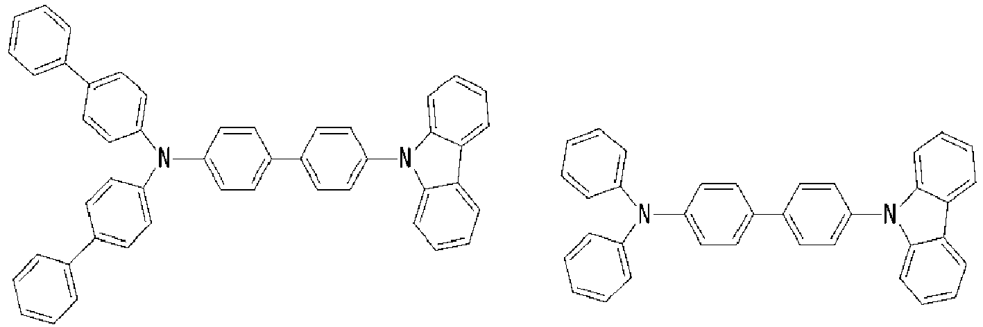


- The emission layer may preferably include a host material including a compound represented by Chemical Formula 2:

- wherein, in Chemical Formula 2,
- R1 to R3 are selected from the group of an amino group, a nitro group, a nitrile group, a C1 to C40 alkyl group, a C2 to C40 alkenyl group, a C2 to C40 alkynyl group, a C5 to C40 aryl group, a C10 to C40 biaryl group, a C1 to C40 heteroaryl group, a C1 to C40 alkoxy group, a C5 to C40 aryloxy group, a C1 to C40 alkylamino group, a C5 to C40 arylamino group, a C5 to C40 diarylamino group, a C5 to C40 heteroarylamino group, a C2 to C40 diheteroarylamino group, a C6 to C40 arylalkyl group, a C6 to C40 heteroarylalkyl group, a C3 to C40 cycloalkyl group, a C1 to C40 halogenalkyl group, a C3 to C40 heterocycloalkyl group, a C3 to C40 alkylsilyl group, a C3 to C40 arylsilyl group, and a C3 to C40 heteroarylsilyl group.
- R1 to R3 may preferably be condensed to an adjacent substituent or may preferably form a ring.
- The compound represented by Chemical Formula 2 includes at least one selected from the compounds represented by Chemical Formula 2-1 to Chemical Formula 2-6:




- The emission layer may preferably further include a dopant material.
- The dopant material may preferably include a red dopant material, a green dopant material, or a red dopant material.
- The first electrode may preferably be an anode, and the second electrode may preferably be a cathode.
- The organic layer may preferably include a hole injection layer (HIL) between the first electrode and the assistance layer, a hole transport layer (HTL) between the hole injection layer (HIL) and the assistance layer, and an electron transport layer (ETL) between the emission layer and the second electrode.
- Features will become apparent to those of skill in the art by describing in detail exemplary embodiments with reference to the attached drawings in which:
-
FIG. 1 illustrates a view of an organic light emitting device according to an exemplary embodiment. -
FIG. 2 illustrates a graph showing a light emitting degree and efficiency of an organic light emitting device according to ExemplaryEmbodiments 1 to 7 and an organic light emitting device according to a Comparative Example. - Embodiments will now be described more fully hereinafter with reference to the accompanying drawings; however, they may preferably be embodied in different forms and should not be construed as limited to the embodiments set forth herein. Rather, these embodiments are provided so that this disclosure will be thorough and complete, and will fully convey exemplary implementations to those skilled in the art.
- In the drawing figures, the dimensions of layers and regions may be exaggerated for clarity of illustration. It will also be understood that when a layer or element is referred to as being "on" another layer or substrate, it can be directly on the other layer or substrate, or intervening layers may also be present. In addition, it will also be understood that when a layer is referred to as being "between" two layers, it can be the only layer between the two layers, or one or more intervening layers may also be present. Like reference numerals refer to like elements throughout.
- In the present exemplary embodiment, unless otherwise specified, "substituted" refers to a hydrogen atom of a compound substituted with a substituent selected from among halogen atoms (F, Br, Cl, or I), a hydroxyl group, an alkoxy group, a nitro group, a cyano group, an amino group, an azido group, an amidino group, a hydrazino group, a hydrazono group, a carbonyl group, a carbamyl group, a thiol group, an ester group, a carboxyl group or its salt, a sulfonic acid group or its salt, a phosphoric acid or its salt, an alkyl group, a C2-C16 alkenyl group, a C2-C16 alkynyl group, an aryl group, a C7-C13 arylalkyl group, a C1-C4 oxyalkyl group, a C1-C20 heteroalkyl group, a C3-C20 heteroaryl alkyl group, a cycloalkyl group, a C3-C15 cycloalkenyl group, a C6-C15 cycloalkynyl group, a heterocycloalkyl group, and combinations thereof.
- Also, unless otherwise specified, "hetero" refers to containing one to three hetero atoms selected from among N, O, S, and P.
- In the drawings, the thickness and/or relative thickness of the elements may be exaggerated in order to clarify embodiments. Also, the expressions related to positions such as "upper part", "lower part", or the like are relatively used for clarification, without limiting absolute positions among the elements.
- An organic light emitting device according to an exemplary embodiment will now be described with reference to
FIG. 1 . -
FIG. 1 illustrates a view of an organic light emitting device according to an exemplary embodiment. - Referring to
FIG. 1 , an organic light emitting device according to the present exemplary embodiment may include afirst electrode 100, asecond electrode 300 facing thefirst electrode 100, and anorganic layer 200 interposed between thefirst electrode 100 and thesecond electrode 300. - A substrate (not shown) may preferably be disposed at the
first electrode 100 side or thesecond electrode 300 side. The substrate may preferably include glass, a polymer, or combinations thereof. - The
first electrode 100 may preferably be an anode, and thesecond electrode 300 may preferably be a cathode. Thefirst electrode 100 and thesecond electrode 300 may preferably be transparent or non-transparent electrodes. For example, thefirst electrode 100 and thesecond electrode 300 may preferably be a transparent electrode made of ITO (indium tin oxide), IZO (indium zinc oxide), or combinations thereof, or a non-transparent electrode made of aluminum (Al), silver (Ag), magnesium (Mg), or combinations thereof. - The
organic layer 200 may preferably include a hole injection layer (HIL) 210, a hole transport layer (HTL) 220, anassistance layer 230, anemission layer 240, and an electron transport layer (ETL) 250 sequentially disposed on thefirst electrode 100. - The hole injection layer (HIL) 210 and the hole transport layer (HTL) 220 may preferably be disposed between the
first electrode 100 and theemission layer 240, such that holes may be easily transmitted from thefirst electrode 100 to theemission layer 240. - The hole injection layer (HIL) 210 may preferably be formed of a hole injection material. For example, the hole injection material may preferably be a phthalocyanine compound such as copper phthalocyanine or the like, m-MTDATA (4,4',4"-tris(3-methylphenylphenylamino)triphenylamine), NPB (N,N'-di(1-naphthyl)-N,N'-diphenylbenzidine), TDATA, 2T-NATA, Pani/DBSA (polyaniline/dodecylbenzene sulfonic acid:polyaniline/dodecylbenzene sulfonic acid), PEDOT/PSS (poly(3,4-ethylene dioxythiophene)/poly(4-styrene sulfonate):poly(3,4-ethylene dioxythiophene)/poly(4-styrene sulfonate)), Pani/CSA (polyaniline/camphor sulfonic acid:polyaniline/camphor sulfonic acid), or Pani/PSS ((polyaniline)/poly(4-styrene sulfonate)).
- The hole transport layer (HTL) 220 may preferably contain a hole transport material. For example, the hole transport material may preferably be a carbazole derivative such as N-phenylcarbazole, polyvinylcarbazole, or the like, and an amine derivative having an aromatic condensed ring such as NPB, N,N'-bis(3-methylphenyl)-N,N'-diphenyl-[1,1-biphenyl]-4,4'-diamine (TPD), tris(4-carbazoyl-9-ylphenyl)amine (TCTA), or the like.
- The
assistance layer 230 may preferably be disposed at the hole transport layer (HTL) 220 and theemission layer 240 to adjust a balance of the charges in the organic light emitting device thereby preventing roll-off generation. - The
assistance layer 230 may preferably include a compound represented by Chemical Formula 1 below.
- In
Chemical Formula 1, L1 and L2 may preferably be independently selected from the group of an amino group, a C1 to C40 alkyl group, a C2 to C40 alkenyl group, a C2 to C40 alkynyl group, , a C5 to C40 aryl group, a C1 to C40 heteroaryl group, a C1 to C40 alkoxy group, a C5 to C40 aryloxy group, a C1 to C40 alkylamino group, a C5 to C40 arylamino group, a C5 to C40 diarylamino group, a C5 to C40 heteroarylamino group, a C2 to C40 diheteroarylamino group, a C6 to C40 arylalkyl group, a C6 to C40 heteroarylalkyl group, a C3 to C40 cycloalkyl group, a C1 to C40 halogenalkyl group, a C3 to C40 heterocycloalkyl group, a C3 to C40 alkylsilyl group, a C3 to C40 arylsilyl group, and a C3 to C40 heteroarylsilyl group, and n may preferably be 0 or 1. - In a preferred embodiment of the present invention L1 and L2 may be independently selected from the group of a C5 to C40 aryl group, a C1 to C40 heteroaryl group, a C5 to C40 diarylamino group, a C2 to C40 diheteroarylamino group, and a C6 to C40 arylalkyl group, preferably a C5 to C16 aryl group, a C4 to C10 heteroaryl group, a C5 to C15 diarylamino group, a C4 to C10 diheteroarylamino group, and a C6 to C15 arylalkyl group, preferably a C6 to C12 aryl group. In preferred embodiments of the present invention, L1 and L2 may be independently selected from the group of phenyl, naphthyl, anthracene and pyrene, more preferably phenyl and naphthyl. In an embodiment of the present invention, the above L1 and L2 groups are substituted with at least one of the substitute substituents defined above, preferably between 1 and 3 substituents.
- When n is 0, L2 and N are directly connected.
- Further, R1 and R2 may preferably be independently selected from the group of an amino group, a nitro group, a nitrile group, a C1 to C40 alkyl group, a C2 to C40 alkenyl group, a C2 to C40 alkynyl group, a C5 to C40 aryl group, a C10 to C40 biaryl group, a C1 to C40 heteroaryl group, a C1 to C40 alkoxy group, a C5 to C40 aryloxy group, a C1 to C40 alkylamino group, a C5 to C40 arylamino group, a C5 to C40 diarylamino group, a C5 to C40 heteroarylamino group, a C2 to C40 diheteroarylamino group, a C6 to C40 arylalkyl group, a C6 to C40 heteroarylalkyl group, a C3 to C40 cycloalkyl group, a C1 to C40 halogenalkyl group, a C3 to C40 heterocycloalkyl group, a C3 to C40 alkylsilyl group, a C3 to C40 arylsilyl group, and a C3 to C40 heteroarylsilyl group.
- In a preferred embodiment of the present invention R1 and R2 may be independently selected from the group of a C5 to C40 aryl group, a C10 to C40 biaryl group, a C1 to C40 heteroaryl group, a C5 to C40 diarylamino group, a C2 to C40 diheteroarylamino group, and a C6 to C40 arylalkyl group, preferably a C5 to C16 aryl group, a C10 to C20 biaryl group, a C4 to C10 heteroaryl group, a C5 to C15 diarylamino group, a C4 to C10 diheteroarylamino group, and a C6 to C15 arylalkyl group, preferably a C6 to C12 aryl group and a C12 to C16 biaryl group. In a preferred embodiment of the present invention, R1 and R2 may be independently selected from the group of phenyl, naphthyl, anthracene, pyrene and biphenyl, more preferably biphenyl, phenyl and naphthyl.
- R1 and R2 may preferably be condensed to the adjacent substituent or may preferably form a ring.
- In an embodiment of the present invention, the above R1 and R2 groups are substituted with at least one of the substitute substituents defined above, preferably between 1 and 3 substituents.
- As examples, a compound represented by
Chemical Formula 1 may preferably be at least one selected from compounds represented by Chemical Formula 1-1 to Chemical Formula 1-9. The compound represented by Chemical Formula 1-1 to Chemical Formula 1-9 may preferably be independently used, at least two or more may preferably be mixed, or at least one may preferably be mixed with a different compound.


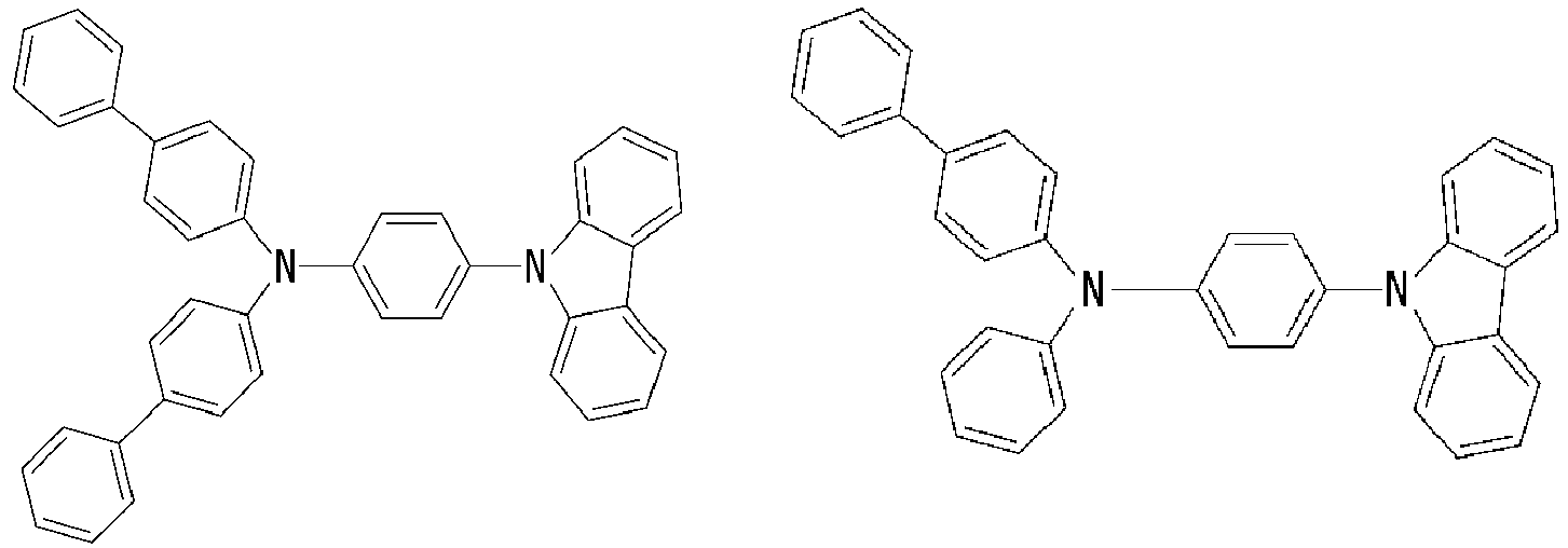


- In an embodiment of the present invention, preferably the compound of
chemical formula 1 makes up greater than 50% by weight of the assistance layer, preferably greater than 75% by weight, preferably between 85% and 100% of the assistance layer. - In an embodiment of the present invention, preferably the assistance layer is from 400Å to 1000Å, preferably 500Å to 900Å, more preferably 600Å to 800Å thick.
- The
emission layer 240 may preferably be made of a host material and a dopant. The dopant may preferably include a material that emits one among primary colors such as red, green, and blue. - The host material may preferably include a compound represented by
Chemical Formula 2.
- In
Chemical Formula 2, R1 to R2 may preferably be selected from the group of an amino group, a nitro group, a nitrile group, a C1 to C40 alkyl group, a C2 to C40 alkenyl group, a C2 to C40 alkynyl group, a C5 to C40 aryl group, a C10 to C40 biaryl group, a C1 to C40 heteroaryl group, a C1 to C40 alkoxy group, a C5 to C40 aryloxy group, a C1 to C40 alkylamino group, a C5 to C40 arylamino group, a C5 to C40 diarylamino group, a C5 to C40 heteroarylamino group, a C2 to C40 diheteroarylamino group, a C6 to C40 arylalkyl group, a C6 to C40 heteroarylalkyl group, a C3 to C40 cycloalkyl group, a C1 to C40 halogenalkyl group, a C3 to C40 heterocycloalkyl group, a C3 to C40 alkylsilyl group, a C3 to C40 arylsilyl group, and a C3 to C40 heteroarylsilyl group. - R3 may preferably be C(H)R1 where R1 is as defined above or may preferably form with R2 a diheteroaryl group with the N atoms that they are bound.
- Also, R1 to R3 may preferably be condensed to an adjacent substituent or may preferably form the ring.
- In a preferred embodiment of the present invention R1 is selected from the group of a C5 to C40 aryl group, a C10 to C40 biaryl group, a C1 to C40 heteroaryl group, a C5 to C40 diarylamino group, a C2 to C40 diheteroarylamino group, and a C6 to C40 arylalkyl group; preferably a C5 to C16 aryl group, a C10 to C20 biaryl group, a C4 to C10 heteroaryl group, a C5 to C15 diarylamino group, a C4 to C10 diheteroarylamino group, and a C6 to C15 arylalkyl group; preferably a C6 to C12 aryl group and a C12 to C16 biaryl group. In a preferred embodiment of the present invention, R1 is selected from the group of phenyl, naphthyl, anthracene, pyrene and biphenyl, more preferably biphenyl, phenyl and naphthyl.
- In a preferred embodiment of the present invention, R2 and R3 form a diheteroaryl group with the N atoms that they are bound to, preferably R2 and R3, the N atoms that they are bound to and the carbon atom linking the N atoms form a substituted or unsubstituted C2 to C40 diheteroaryl group, more preferably a substituted or unsubstituted C3 to C15 diheteroaryl group, more preferably a substituted or unsubstituted C4 to C10 a substituted or unsubstituted. For example, a substituted or unsubstituted pyrimidine group or a substituted or unsubstituted quinazoline group.
- In an embodiment of the present invention, the above R1 to R3 groups in
Chemical Formula 2 are substituted with at least one of the substitute substituents defined above, preferably between 1 and 3 substituents. - In an embodiment of the present invention the ring formed by R2 and R3 is substituted with at least one, preferably between 1 and 3 substituents independently selected from the group of a C5 to C40 aryl group, a C10 to C40 biaryl group, a C1 to C40 heteroaryl group, a C5 to C40 diarylamino group, a C2 to C40 diheteroarylamino group, and a C6 to C40 arylalkyl group, preferably a C5 to C16 aryl group, a C10 to C20 biaryl group, a C4 to C10 heteroaryl group, a C5 to C15 diarylamino group, a C4 to C10 diheteroarylamino group, and a C6 to C15 arylalkyl group, preferably a C6 to C12 aryl group and a C12 to C16 biaryl group. In a preferred embodiments of the present invention, the ring formed by R2 and R3 is substituted with at least one, preferably between 1 and 3, more preferably 1, substituent independently selected from the group of phenyl, naphthyl, anthracene, pyrene, biphenyl and a phenylnapthyl group, more preferably biphenyl, phenyl, phenylnapthyl group and naphthyl. In an embodiment of the present invention the ring formed by R2 and R3 is preferably substituted at a carbon adjacent to one of the N atoms, e.g. at the 4-position when the ring is quinazoline or the 4- or 6-position when the ring is pyrimidine.
- For example, the compound represented by
Chemical Formula 2 may preferably be at least one selected from compounds represented by Chemical Formula 2-1 to Chemical Formula 2-6. The compound represented by Chemical Formula 2-1 to Chemical Formula 2-6 may preferably be independently used, at least two or more may preferably be mixed, or at least one may preferably be mixed with a different compound.

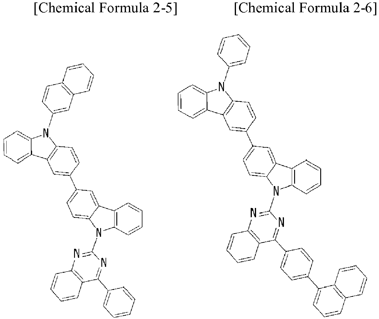
- As examples, a red dopant may preferably include PtOEP, Ir(piq)3, Btp2Ir(acac), DCJTB, or the like.
- As examples, a green dopant may preferably include Ir(ppy)3(ppy=phenyl), Ir(ppy)2(acac), Ir(mpyp)3, C545T, or the like.
- As examples, a blue dopant may preferably include F2Irpic, (F2ppy)2Ir(tmd), Ir(dfppz)3, ter-fluorene, 4,4'-bis(4-diphenylaminostyryl)biphenyl (DPAVBi), 2,5,8,11-tetra-tert-butyl perylene (TBP), or the like.
- For example, the
emission layer 240 of the organic light emitting device may preferably include the compound represented byChemical Formula 2 as the host material, and may preferably be a red emission layer doped with the red dopant. - In an embodiment of the present invention the weight ratio of the host material and the dopant material is from 1.0:0.01 to 1.0:0.1, preferably from 1.0:0.02 to 1.0:0.06.
- In an embodiment of the present invention, preferably the emission layer is from 100Å to 700Å, preferably 200Å to 600Å, more preferably 300Å to 500Å, thick.
- The electron transport layer (ETL) 250 may preferably be disposed between the
emission layer 240 and thesecond electrode 300. Thereby, electrons may be easily injected from thesecond electrode 300 to theemission layer 240. The electron transport layer (ETL) 250 may include an electron transport material. For example, the disclosed material may be a quinoline derivative such as aluminum tris(8-hydroxyquinoline) (Alq3), TAZ, or BAlq. - The electron injection layer (EIL) may preferably be disposed between the electron transport layer (ETL) 250 and the
second electrode 300 such that the electrons may be easily injected from thesecond electrode 300 to theemission layer 240. The electron injection layer (EIL) may preferably be made of an electron injection material, for example, lithium fluoride (LiF), lithium quinolate (Liq), oxadiazole, triazole, or triazine. - As described above, the
assistance layer 230 made of the compound represented byChemical Formula 1 may preferably be disposed between the hole transport layer (HTL) 220 and theemission layer 240. The compound represented byChemical Formula 2 may preferably be used as the host material of theemission layer 240, thereby adjusting the balance of the elements in the organic light emitting device. - Accordingly, the generation of a roll-off phenomenon may be reduced. Further, the efficiency of the organic device may be improved, and the life-span may be increased.
- The following Examples and Comparative Examples are provided in order to highlight characteristics of one or more embodiments, but it is to be understood that the Examples and Comparative Examples are not to be construed as limiting the scope of the embodiments,. Further, it is to be understood that the embodiments are not limited to the particular details described in the Examples and Comparative Examples.
- ITO (indium tin oxide) was cut into a size of 50 mm x 50 mm x 0.5 mm and was subjected to an ultrasonic wave cleaning process for about ten minutes using isopropyl alcohol and pure water to form an anode.
- 2T-NATA (4,4',4"- tris[2-naphthyl(phenyl)amino]triphenylamine) having a thickness of 100 Å was vacuum-deposited on the anode to form a hole injection layer (HIL). NPB (N,N'- di(1-naphthyl)-N,N'-diphenylbenzidine) having a thickness of 1350 Å was vacuum-deposited on the hole injection layer (HIL) to form a hole transport layer (HTL).
- The compound represented by Chemical Formula 1-3 and having a thickness of 700 Å was vacuum-deposited on the hole transport layer (HTL) to form an assistance layer. The compound represented by Chemical Formula 2-2, serving as a host material, and Ir(piq)3 (Tris[1-phenylisoquinoline-C2,N]iridium(III), serving as a red phosphorescent dopant of a dopant material, were simultaneously subjected to vacuum deposition in a weight ratio of 1:0.04 to form an emission layer having a thickness of 400Å on the assistance layer.
- Alq3 (Tris(8-hydroxyquinolinato)aluminum) was subjected to vacuum deposition to form an electron transport layer (ETL) with a thickness of 300 Å on the emission layer. Then, Al was subjected to vacuum deposition to form a cathode with a thickness of 1200 Å on the electron transport layer (ETL).
- Thereby, the organic light emitting device is manufactured.
- An organic light emitting diode device was manufactured by using substantially the same method as in
Exemplary Embodiment 1, except for using the compound represented by Chemical Formula 1-1 as the assistance layer. - An organic light emitting diode device was manufactured by using substantially the same method as in
Exemplary Embodiment 1, except for using the compound represented by Chemical Formula 1-2 as the assistance layer. - An organic light emitting diode device was manufactured by using substantially the same method as in
Exemplary Embodiment 1, except for using the compound represented by Chemical Formula 1-4 as the assistance layer. - An organic light emitting diode device was manufactured by using substantially the same method as in
Exemplary Embodiment 1, except for using the compound represented by Chemical Formula 1-5 as the assistance layer. - An organic light emitting diode device was manufactured by using substantially the same method as in
Exemplary Embodiment 1, except for using the compound represented by Chemical Formula 2-1 as the host material of the emission layer. - An organic light emitting diode device was manufactured by using substantially the same method as in
Exemplary Embodiment 2, except for using the compound represented by Chemical Formula 2-1 as the host material of the emission layer. - An organic light emitting diode device was manufactured by using substantially the same method as in
Exemplary Embodiment 1, except for vacuum-depositing NPB with a thickness of 2100 Å to form the hole transport layer (HTL) and using CBP (4,4'-Bis(9-carbazolyl)-1,1'-biphenyl) as the host material of the emission layer without the assistance layer. - The driving voltage, the efficiency, and the life-span of the organic light emitting device according to
Exemplary Embodiments 1 to 7 and the organic light emitting device according to the comparative example were measured. The measurement results are shown in Table 1.(Table 1) Assistance layer material Host material Driving voltage (V) Current efficiency (Cd/A) Life-span (T97, hours) Comparative Example - CBP 4.8 27.6 302 Exemplary Embodiment 1Chemical Formula 1-3 Chemical Formula 2-2 4.0 43.9 730 Exemplary Embodiment 2Chemical Formula 1-1 Chemical Formula 2-2 4.5 33.9 520 Exemplary Embodiment 3Chemical Formula 1-2 Chemical Formula 2-2 4.3 38.8 601 Exemplary Embodiment 4 Chemical Formula 1-4 Chemical Formula 2-2 4.3 32.7 528 Exemplary Embodiment 5 Chemical Formula 1-5 Chemical Formula 2-2 4.5 34.3 545 Exemplary Embodiment 6 Chemical Formula 1-3 Chemical Formula 2-1 4.2 41.5 684 Exemplary Embodiment 7 Chemical Formula 1-1 Chemical Formula 2-1 4.4 35.1 560 - Referring to Table 1, in the organic light emitting device according to
Exemplary Embodiments 1 to 7, the driving voltage is shown to be lower, and the current efficiency and the life-span are shown to be greater, compared with the organic light emitting device according to the Comparative Example. - The efficiency according to a light emitting degree for the organic light emitting device according to
Exemplary Embodiments 1 to 7 and the organic light emitting device according to the comparative example was measured. The measurement results are shown inFIG. 2 . -
FIG. 2 illustrates a graph showing a light emitting degree (luminance, in units of cd/m2) and efficiency (cd/A) of an organic light emitting device according toExemplary Embodiments 1 to 7 and an organic light emitting device according to a Comparative Example. - Referring to
FIG. 2 , in the organic light emitting device according to the Comparative Example, compared with the organic light emitting device according toExemplary Embodiments 1 to 7, as the light emitting degree was increased, the efficiency was decreased. - In the case of the organic light emitting device according to the Comparative Example,, the driving voltage was decreased by the hole injection layer (HIL) such that the initial efficiency was shown to be good. However, without being bound to any particular theory, it is believed that the charge balance in the elements was poor such that the roll-off phenomenon was generated, and thereby the efficiency was gradually reduced.
- In contrast, by using the assistance layer in the organic light emitting devices according to
Exemplary Embodiments 1 to 7, as the light emitting degree was increased, the reduction of the efficiency was slight such that it may be confirmed that the generation of the roll-off phenomenon may be reduced or avoided. - By way of summation and review, in an organic light emitting device, characteristics of a material forming the organic layer may largely affect electrical characteristics of the organic light emitting device.
- Embodiments provide an organic light emitting device having high efficiency and a long life-span. According embodiments, by forming an assistance layer between the emission layer and the hole transport layer (HTL) including the compound represented by
Chemical Formula 1 and the host in the emission layer including the compound represented byChemical Formula 2, the efficiency of the organic light emitting device may be improved and the life-span may be increased. - Example embodiments have been disclosed herein, and although specific terms are employed, they are used and are to be interpreted in a generic and descriptive sense only and not for purpose of limitation. In some instances, as would be apparent to one of ordinary skill in the art as of the filing of the present application, features, characteristics, and/or elements described in connection with a particular embodiment may be used singly or in combination with features, characteristics, and/or elements described in connection with other embodiments unless otherwise specifically indicated. Accordingly, it will be understood by those of skill in the art that various changes in form and details may be made without departing from the scope thereof as set forth in the following claims.
Claims (15)
- An organic light emitting device, comprising:a first electrode and a second electrode facing each other; andan organic layer between the first electrode and the second electrode,wherein the organic layer includes an assistance layer on the first electrode and an emission layer on the assistance layer, the assistance layer including a compound represented by Chemical Formula 1:
 wherein, in Chemical Formula 1, L1 and L2 are independently selected from the group of an amino group, a C1 to C40 alkyl group, a C2 to C40 alkenyl group, a C2 to C40 alkynyl group, a C5 to C40 aryl group, a C1 to C40 heteroaryl group, a C1 to C40 alkoxy group, a C5 to C40 aryloxy group, a C1 to C40 alkylamino group, a C5 to C40 arylamino group, a C5 to C40 diarylamino group, a C5 to C40 heteroarylamino group, a C2 to C40 diheteroarylamino group, a C6 to C40 arylalkyl group, a C6 to C40 heteroarylalkyl group, a C3 to C40 cycloalkyl group, a C1 to C40 halogenalkyl group, a C3 to C40 heterocycloalkyl group, a C3 to C40 alkylsilyl group, a C3 to C40 arylsilyl group, and a C3 to C40 heteroarylsilyl group,R1 and R2 are independently selected from the group of an amino group, a nitro group, a nitrile group, a C1 to C40 alkyl group, a C2 to C40 alkenyl group, a C2 to C40 alkynyl group, a C5 to C40 aryl group, a C10 to C40 biaryl group, a C1 to C40 heteroaryl group, a C1 to C40 alkoxy group, a C5 to C40 aryloxy group, a C1 to C40 alkylamino group, a C5 to C40 arylamino group, a C5 to C40 diarylamino group, a C5 to C40 heteroarylamino group, a C2 to C40 diheteroarylamino group, a C6 to C40 arylalkyl group, a C6 to C40 heteroarylalkyl group, a C3 to C40 cycloalkyl group, a C1 to C40 halogenalkyl group, a C3 to C40 heterocycloalkyl group, a C3 to C40 alkylsilyl group, a C3 to C40 arylsilyl group, and a C3 to C40 heteroarylsilyl group, andn is 0 or 1.
 - The organic light emitting device as claimed in claim 1, wherein in the compound represented by Chemical Formula 1,
n is 0, and, optionally,
R1 or R2 is condensed to an adjacent substituent or R1 and R2 form a ring. - The organic light emitting device as claimed in claim 1 or claim 2,
wherein L1 and L2 are independently selected from the group of a C5 to C40 aryl group, a C1 to C40 heteroaryl group, a C5 to C40 diarylamino group, a C2 to C40 diheteroarylamino group, and a C6 to C40 arylalkyl group; preferably a C5 to C16 aryl group, a C4 to C10 heteroaryl group, a C5 to C15 diarylamino group, a C4 to C10 diheteroarylamino group, and a C6 to C15 arylalkyl group - The organic light emitting device as claimed in any of claims 1 to 3,
wherein R1 and R2 are independently selected from the group of a C5 to C40 aryl group, a C10 to C40 biaryl group, a C1 to C40 heteroaryl group, a C5 to C40 diarylamino group, a C2 to C40 diheteroarylamino group, and a C6 to C40 arylalkyl group; preferably a C5 to C16 aryl group, a C10 to C20 biaryl group, a C4 to C10 heteroaryl group, a C5 to C15 diarylamino group, a C4 to C10 diheteroarylamino group, and a C6 to C15 arylalkyl group. - The organic light emitting device as claimed in any of claims 1 to 4,
wherein L1 and L2 are independently a C6 to C12 aryl group and R1 and R2 are independently a C6 to C12 aryl group or a C12 to C16 biaryl group. - The organic light emitting device as claimed in any of claims 1 to 5 in claim 2, wherein the compound represented by Chemical Formula 1 includes at least one selected from the compounds represented by Chemical Formula 1-1 to Chemical Formula 1-9:


- The organic light emitting device as claimed in any of claims 1 to 6,
wherein the emission layer includes a host material including a compound represented by Chemical Formula 2: R1 to R2 are selected from the group of an amino group, a nitro group, a nitrile group, a C1 to C40 alkyl group, a C2 to C40 alkenyl group, a C2 to C40 alkynyl group, a C5 to C40 aryl group, a C10 to C40 biaryl group, a C1 to C40 heteroaryl group, a C1 to C40 alkoxy group, a C5 to C40 aryloxy group, a C1 to C40 alkylamino group, a C5 to C40 arylamino group, a C5 to C40 diarylamino group, a C5 to C40 heteroarylamino group, a C2 to C40 diheteroarylamino group, a C6 to C40 arylalkyl group, a C6 to C40 heteroarylalkyl group, a C3 to C40 cycloalkyl group, a C1 to C40 halogenalkyl group, a C3 to C40 heterocycloalkyl group, a C3 to C40 alkylsilyl group, a C3 to C40 arylsilyl group, and a C3 to C40 heteroarylsilyl group;R3 is C(H)R1 where R1 is as defined above,or where R2 and R3 are condensed to form a ring.
 - The organic light emitting device as claimed in claim 7, wherein R1 is selected from the group of a C5 to C40 aryl group, a C10 to C40 biaryl group, a C1 to C40 heteroaryl group, a C5 to C40 diarylamino group, a C2 to C40 diheteroarylamino group, and a C6 to C40 arylalkyl group, preferably a C5 to C16 aryl group, a C10 to C20 biaryl group, a C4 to C10 heteroaryl group, a C5 to C15 diarylamino group, a C4 to C10 diheteroarylamino group, and a C6 to C15 arylalkyl group, preferably a C6 to C12 aryl group and a C12 to C16 biaryl group.
- The organic light emitting device as claimed in claim 7 or claim 8,
wherein R2 and R3 form a diheteroaryl group with the N atoms that they are bound to. - The organic light emitting device as claimed in any of claims 5 to 9,
wherein the compound represented by Chemical Formula 2 includes at least one selected from the compounds represented by Chemical Formula 2-1 to Chemical Formula 2-6:


- The organic light emitting device as claimed in any of claims 1 to 9,
wherein the emission layer further includes a dopant material, optionally wherein the dopant material includes a red dopant material, a green dopant material, or a red dopant material. - The organic light emitting device as claimed in claim 11, wherein the weight ratio of the host material and the dopant material is from 1.0:0.01 to 1.0:0.1, preferably from 1.0:0.02 to 1.0:0.06.
- The organic light emitting device as claimed in any of claims 1 to 12,
wherein the emission layer is from 100Å to 700Å thick, preferably 200Å to 600Å, more preferably 300Å to 500Å; and/or the assistance layer is from 400Å to 1000Å thick, preferably 500Å to 900Å, more preferably 600Å to 800Å thick. - The organic light emitting device as claimed in any of claims 1 to 13, wherein the first electrode is an anode, and the second electrode is a cathode.
- The organic light emitting device as claimed in any of claims 1 to 14, wherein the organic layer includes:a hole injection layer (HIL) between the first electrode and the assistance layer;a hole transport layer (HTL) between the hole injection layer (HIL) and the assistance layer; andan electron transport layer (ETL) between the emission layer and the second electrode.
Applications Claiming Priority (1)
| Application Number | Priority Date | Filing Date | Title |
|---|---|---|---|
| KR1020130083012A KR101566434B1 (en) | 2013-07-15 | 2013-07-15 | Organic light emitting device |
Publications (2)
| Publication Number | Publication Date |
|---|---|
| EP2826837A1 true EP2826837A1 (en) | 2015-01-21 |
| EP2826837B1 EP2826837B1 (en) | 2019-09-11 |
Family
ID=51176970
Family Applications (1)
| Application Number | Title | Priority Date | Filing Date |
|---|---|---|---|
| EP14177131.1A Active EP2826837B1 (en) | 2013-07-15 | 2014-07-15 | Organic light emitting device |
Country Status (5)
| Country | Link |
|---|---|
| US (1) | US20150014657A1 (en) |
| EP (1) | EP2826837B1 (en) |
| KR (1) | KR101566434B1 (en) |
| CN (1) | CN104300093B (en) |
| TW (1) | TWI682985B (en) |
Families Citing this family (4)
| Publication number | Priority date | Publication date | Assignee | Title |
|---|---|---|---|---|
| KR102370354B1 (en) * | 2015-04-29 | 2022-03-07 | 삼성디스플레이 주식회사 | Organic light emitting device comprising the same |
| KR102641027B1 (en) * | 2017-05-31 | 2024-02-28 | 롬엔드하스전자재료코리아유한회사 | Organic Electroluminescent Device |
| KR102008583B1 (en) * | 2017-12-05 | 2019-08-07 | 부산대학교 산학협력단 | Fluorene Derivative Compounds, Organic Light Emitting Devices using thereof, and Photovoltaic Device using thereof |
| CN113461594B (en) * | 2021-05-20 | 2024-06-21 | 南京邮电大学 | Organic light-emitting memory material and bistable OLED memory using same |
Citations (2)
| Publication number | Priority date | Publication date | Assignee | Title |
|---|---|---|---|---|
| DE102010048497A1 (en) * | 2010-10-14 | 2012-04-19 | Merck Patent Gmbh | Formulations for organic electroluminescent devices |
| WO2013017192A1 (en) * | 2011-08-03 | 2013-02-07 | Merck Patent Gmbh | Materials for electronic devices |
Family Cites Families (14)
| Publication number | Priority date | Publication date | Assignee | Title |
|---|---|---|---|---|
| US223505A (en) * | 1880-01-13 | Lawn-edge mower | ||
| US6242115B1 (en) * | 1997-09-08 | 2001-06-05 | The University Of Southern California | OLEDs containing thermally stable asymmetric charge carrier materials |
| JPH11329737A (en) * | 1998-03-13 | 1999-11-30 | Taiho Ind Co Ltd | Organic multilayer electroluminescence device and method for synthesizing structure for organic multilayer electroluminescence device |
| TW545080B (en) * | 2000-12-28 | 2003-08-01 | Semiconductor Energy Lab | Light emitting device and method of manufacturing the same |
| US20070215889A1 (en) * | 2006-03-20 | 2007-09-20 | Semiconductor Energy Laboratory Co., Ltd. | Aromatic amine compound, and light-emitting element, light-emitting device, and electronic appliance using the aromatic amine compound |
| TWI510598B (en) * | 2007-03-08 | 2015-12-01 | Universal Display Corp | Phosphorescent materials |
| JP2009037981A (en) * | 2007-08-03 | 2009-02-19 | Idemitsu Kosan Co Ltd | Organic EL device and method for manufacturing organic EL device |
| KR100922759B1 (en) * | 2008-02-26 | 2009-10-21 | 삼성모바일디스플레이주식회사 | Organic light emitting device |
| KR101506999B1 (en) * | 2009-11-03 | 2015-03-31 | 제일모직 주식회사 | Compound for organic photoelectric device and organic photoelectric device including the same |
| DE102010010481A1 (en) * | 2010-03-06 | 2011-09-08 | Merck Patent Gmbh | Organic electroluminescent device |
| KR20110122051A (en) * | 2010-05-03 | 2011-11-09 | 제일모직주식회사 | Compound for organic photoelectric device and organic photoelectric device comprising same |
| WO2012108389A1 (en) * | 2011-02-07 | 2012-08-16 | 出光興産株式会社 | Biscarbazole derivative and organic electroluminescent element using same |
| KR101427611B1 (en) * | 2011-03-08 | 2014-08-11 | 롬엔드하스전자재료코리아유한회사 | Novel compounds for organic electronic material and organic electroluminescence device using the same |
| JP2015216136A (en) * | 2012-08-17 | 2015-12-03 | 出光興産株式会社 | Organic electroluminescence device |
-
2013
- 2013-07-15 KR KR1020130083012A patent/KR101566434B1/en active Active
-
2014
- 2014-05-09 US US14/273,958 patent/US20150014657A1/en not_active Abandoned
- 2014-07-11 TW TW103123904A patent/TWI682985B/en active
- 2014-07-14 CN CN201410334147.4A patent/CN104300093B/en active Active
- 2014-07-15 EP EP14177131.1A patent/EP2826837B1/en active Active
Patent Citations (2)
| Publication number | Priority date | Publication date | Assignee | Title |
|---|---|---|---|---|
| DE102010048497A1 (en) * | 2010-10-14 | 2012-04-19 | Merck Patent Gmbh | Formulations for organic electroluminescent devices |
| WO2013017192A1 (en) * | 2011-08-03 | 2013-02-07 | Merck Patent Gmbh | Materials for electronic devices |
Non-Patent Citations (3)
| Title |
|---|
| KUWABARA Y ET AL: "THERMALLY STABLE MULTILAYERED ORGANIC EL DEVICES USING NOVEL STARBURST MOLECULES, 4,4',4''-TRI(N-CARBAZOYL)TRIPHENYLAMINE (TCTA) AND 4,4',4''-TRIS(3-METHYLPHENYLPHENYLAMINO)TRIPHENYLAMINE (M-MTDATA), AS HOLE-TRANSPORT MATERIALS", ADVANCED MATERIALS, WILEY - V C H VERLAG GMBH & CO. KGAA, DE, vol. 6, no. 9, 1 September 1994 (1994-09-01), pages 677 - 679, XP001203489, ISSN: 0935-9648, DOI: 10.1002/ADMA.19940060913 * |
| NOMURA M. ET AL: "Synthesis of thermally stable and hole-transporting amorphous molecule having four carbazole moieties", SYNTHETIC METALS, ELSEVIER SEQUOIA, LAUSANNE, CH, vol. 148, no. 2, 31 January 2005 (2005-01-31), pages 155 - 160, XP027758460, ISSN: 0379-6779, [retrieved on 20050131] * |
| WANG QI ET AL: "Highly efficient single-emitting-layer white organic light-emitting diodes with reduced efficiency roll-off", APPLIED PHYSICS LETTERS, AMERICAN INSTITUTE OF PHYSICS, US, vol. 94, no. 10, 9 March 2009 (2009-03-09), pages 103503 - 103503, XP012118367, ISSN: 0003-6951, DOI: 10.1063/1.3097028 * |
Also Published As
| Publication number | Publication date |
|---|---|
| TWI682985B (en) | 2020-01-21 |
| KR20150008709A (en) | 2015-01-23 |
| CN104300093B (en) | 2020-11-10 |
| CN104300093A (en) | 2015-01-21 |
| TW201512370A (en) | 2015-04-01 |
| US20150014657A1 (en) | 2015-01-15 |
| EP2826837B1 (en) | 2019-09-11 |
| KR101566434B1 (en) | 2015-11-06 |
Similar Documents
| Publication | Publication Date | Title |
|---|---|---|
| EP2012375B1 (en) | Organic light emitting device | |
| KR101799077B1 (en) | An organic light emitting diode and method for preparing the same | |
| KR102329051B1 (en) | Organic compound and organic light emitting diode device including the same | |
| KR102083434B1 (en) | Organic light emitting device and manufacturing method thereof | |
| KR101869062B1 (en) | Organic light emitting device | |
| CN106560935A (en) | Organic electroluminescent device | |
| US8421326B2 (en) | Electrode, method of preparing the same, and electronic device including the electrode | |
| US9991446B2 (en) | Organic light emitting device and display device having the same | |
| KR20120049639A (en) | Organic light emitting device | |
| KR102090704B1 (en) | Organic light emitting device | |
| US10177334B2 (en) | Organic light emitting device and display device having the same | |
| KR102083985B1 (en) | Organic light emitting diode and method for preparing the same | |
| US20140353596A1 (en) | Organic light-emitting diode | |
| KR20140099776A (en) | An organic light emitting diode | |
| EP2259362A1 (en) | Organic light emitting diode | |
| KR20130007159A (en) | Organic light emitting device | |
| KR101473308B1 (en) | Organic light emitting device | |
| EP2772955A2 (en) | Organic light emitting diode device | |
| EP2826837B1 (en) | Organic light emitting device | |
| KR101642117B1 (en) | Organic light emitting device | |
| US20120012828A1 (en) | Organic light-emitting device | |
| US9755176B2 (en) | Organic light-emitting device | |
| KR101879832B1 (en) | An organic light emitting diode | |
| KR102251735B1 (en) | Material for organic light emitting device, organic light emitting device, and display device including the same | |
| KR102177211B1 (en) | Organic light emitting device |
Legal Events
| Date | Code | Title | Description |
|---|---|---|---|
| 17P | Request for examination filed |
Effective date: 20140715 |
|
| AK | Designated contracting states |
Kind code of ref document: A1 Designated state(s): AL AT BE BG CH CY CZ DE DK EE ES FI FR GB GR HR HU IE IS IT LI LT LU LV MC MK MT NL NO PL PT RO RS SE SI SK SM TR |
|
| AX | Request for extension of the european patent |
Extension state: BA ME |
|
| PUAI | Public reference made under article 153(3) epc to a published international application that has entered the european phase |
Free format text: ORIGINAL CODE: 0009012 |
|
| R17P | Request for examination filed (corrected) |
Effective date: 20150702 |
|
| RBV | Designated contracting states (corrected) |
Designated state(s): AL AT BE BG CH CY CZ DE DK EE ES FI FR GB GR HR HU IE IS IT LI LT LU LV MC MK MT NL NO PL PT RO RS SE SI SK SM TR |
|
| RAP1 | Party data changed (applicant data changed or rights of an application transferred) |
Owner name: SAMSUNG DISPLAY CO., LTD. |
|
| TPAC | Observations filed by third parties |
Free format text: ORIGINAL CODE: EPIDOSNTIPA |
|
| STAA | Information on the status of an ep patent application or granted ep patent |
Free format text: STATUS: EXAMINATION IS IN PROGRESS |
|
| 17Q | First examination report despatched |
Effective date: 20170804 |
|
| GRAP | Despatch of communication of intention to grant a patent |
Free format text: ORIGINAL CODE: EPIDOSNIGR1 |
|
| STAA | Information on the status of an ep patent application or granted ep patent |
Free format text: STATUS: GRANT OF PATENT IS INTENDED |
|
| INTG | Intention to grant announced |
Effective date: 20190222 |
|
| GRAS | Grant fee paid |
Free format text: ORIGINAL CODE: EPIDOSNIGR3 |
|
| GRAA | (expected) grant |
Free format text: ORIGINAL CODE: 0009210 |
|
| STAA | Information on the status of an ep patent application or granted ep patent |
Free format text: STATUS: THE PATENT HAS BEEN GRANTED |
|
| AK | Designated contracting states |
Kind code of ref document: B1 Designated state(s): AL AT BE BG CH CY CZ DE DK EE ES FI FR GB GR HR HU IE IS IT LI LT LU LV MC MK MT NL NO PL PT RO RS SE SI SK SM TR |
|
| REG | Reference to a national code |
Ref country code: GB Ref legal event code: FG4D |
|
| REG | Reference to a national code |
Ref country code: CH Ref legal event code: EP |
|
| REG | Reference to a national code |
Ref country code: AT Ref legal event code: REF Ref document number: 1178441 Country of ref document: AT Kind code of ref document: T Effective date: 20190915 |
|
| REG | Reference to a national code |
Ref country code: DE Ref legal event code: R096 Ref document number: 602014053321 Country of ref document: DE Ref country code: IE Ref legal event code: FG4D |
|
| REG | Reference to a national code |
Ref country code: NL Ref legal event code: MP Effective date: 20190911 |
|
| REG | Reference to a national code |
Ref country code: LT Ref legal event code: MG4D |
|
| PG25 | Lapsed in a contracting state [announced via postgrant information from national office to epo] |
Ref country code: FI Free format text: LAPSE BECAUSE OF FAILURE TO SUBMIT A TRANSLATION OF THE DESCRIPTION OR TO PAY THE FEE WITHIN THE PRESCRIBED TIME-LIMIT Effective date: 20190911 Ref country code: LT Free format text: LAPSE BECAUSE OF FAILURE TO SUBMIT A TRANSLATION OF THE DESCRIPTION OR TO PAY THE FEE WITHIN THE PRESCRIBED TIME-LIMIT Effective date: 20190911 Ref country code: BG Free format text: LAPSE BECAUSE OF FAILURE TO SUBMIT A TRANSLATION OF THE DESCRIPTION OR TO PAY THE FEE WITHIN THE PRESCRIBED TIME-LIMIT Effective date: 20191211 Ref country code: NO Free format text: LAPSE BECAUSE OF FAILURE TO SUBMIT A TRANSLATION OF THE DESCRIPTION OR TO PAY THE FEE WITHIN THE PRESCRIBED TIME-LIMIT Effective date: 20191211 Ref country code: HR Free format text: LAPSE BECAUSE OF FAILURE TO SUBMIT A TRANSLATION OF THE DESCRIPTION OR TO PAY THE FEE WITHIN THE PRESCRIBED TIME-LIMIT Effective date: 20190911 Ref country code: SE Free format text: LAPSE BECAUSE OF FAILURE TO SUBMIT A TRANSLATION OF THE DESCRIPTION OR TO PAY THE FEE WITHIN THE PRESCRIBED TIME-LIMIT Effective date: 20190911 |
|
| PG25 | Lapsed in a contracting state [announced via postgrant information from national office to epo] |
Ref country code: RS Free format text: LAPSE BECAUSE OF FAILURE TO SUBMIT A TRANSLATION OF THE DESCRIPTION OR TO PAY THE FEE WITHIN THE PRESCRIBED TIME-LIMIT Effective date: 20190911 Ref country code: GR Free format text: LAPSE BECAUSE OF FAILURE TO SUBMIT A TRANSLATION OF THE DESCRIPTION OR TO PAY THE FEE WITHIN THE PRESCRIBED TIME-LIMIT Effective date: 20191212 Ref country code: AL Free format text: LAPSE BECAUSE OF FAILURE TO SUBMIT A TRANSLATION OF THE DESCRIPTION OR TO PAY THE FEE WITHIN THE PRESCRIBED TIME-LIMIT Effective date: 20190911 Ref country code: ES Free format text: LAPSE BECAUSE OF FAILURE TO SUBMIT A TRANSLATION OF THE DESCRIPTION OR TO PAY THE FEE WITHIN THE PRESCRIBED TIME-LIMIT Effective date: 20190911 Ref country code: LV Free format text: LAPSE BECAUSE OF FAILURE TO SUBMIT A TRANSLATION OF THE DESCRIPTION OR TO PAY THE FEE WITHIN THE PRESCRIBED TIME-LIMIT Effective date: 20190911 |
|
| REG | Reference to a national code |
Ref country code: AT Ref legal event code: MK05 Ref document number: 1178441 Country of ref document: AT Kind code of ref document: T Effective date: 20190911 |
|
| PG25 | Lapsed in a contracting state [announced via postgrant information from national office to epo] |
Ref country code: EE Free format text: LAPSE BECAUSE OF FAILURE TO SUBMIT A TRANSLATION OF THE DESCRIPTION OR TO PAY THE FEE WITHIN THE PRESCRIBED TIME-LIMIT Effective date: 20190911 Ref country code: PL Free format text: LAPSE BECAUSE OF FAILURE TO SUBMIT A TRANSLATION OF THE DESCRIPTION OR TO PAY THE FEE WITHIN THE PRESCRIBED TIME-LIMIT Effective date: 20190911 Ref country code: AT Free format text: LAPSE BECAUSE OF FAILURE TO SUBMIT A TRANSLATION OF THE DESCRIPTION OR TO PAY THE FEE WITHIN THE PRESCRIBED TIME-LIMIT Effective date: 20190911 Ref country code: IT Free format text: LAPSE BECAUSE OF FAILURE TO SUBMIT A TRANSLATION OF THE DESCRIPTION OR TO PAY THE FEE WITHIN THE PRESCRIBED TIME-LIMIT Effective date: 20190911 Ref country code: PT Free format text: LAPSE BECAUSE OF FAILURE TO SUBMIT A TRANSLATION OF THE DESCRIPTION OR TO PAY THE FEE WITHIN THE PRESCRIBED TIME-LIMIT Effective date: 20200113 Ref country code: RO Free format text: LAPSE BECAUSE OF FAILURE TO SUBMIT A TRANSLATION OF THE DESCRIPTION OR TO PAY THE FEE WITHIN THE PRESCRIBED TIME-LIMIT Effective date: 20190911 Ref country code: NL Free format text: LAPSE BECAUSE OF FAILURE TO SUBMIT A TRANSLATION OF THE DESCRIPTION OR TO PAY THE FEE WITHIN THE PRESCRIBED TIME-LIMIT Effective date: 20190911 |
|
| PG25 | Lapsed in a contracting state [announced via postgrant information from national office to epo] |
Ref country code: SK Free format text: LAPSE BECAUSE OF FAILURE TO SUBMIT A TRANSLATION OF THE DESCRIPTION OR TO PAY THE FEE WITHIN THE PRESCRIBED TIME-LIMIT Effective date: 20190911 Ref country code: CZ Free format text: LAPSE BECAUSE OF FAILURE TO SUBMIT A TRANSLATION OF THE DESCRIPTION OR TO PAY THE FEE WITHIN THE PRESCRIBED TIME-LIMIT Effective date: 20190911 Ref country code: IS Free format text: LAPSE BECAUSE OF FAILURE TO SUBMIT A TRANSLATION OF THE DESCRIPTION OR TO PAY THE FEE WITHIN THE PRESCRIBED TIME-LIMIT Effective date: 20200224 Ref country code: SM Free format text: LAPSE BECAUSE OF FAILURE TO SUBMIT A TRANSLATION OF THE DESCRIPTION OR TO PAY THE FEE WITHIN THE PRESCRIBED TIME-LIMIT Effective date: 20190911 |
|
| REG | Reference to a national code |
Ref country code: DE Ref legal event code: R097 Ref document number: 602014053321 Country of ref document: DE |
|
| PLBE | No opposition filed within time limit |
Free format text: ORIGINAL CODE: 0009261 |
|
| STAA | Information on the status of an ep patent application or granted ep patent |
Free format text: STATUS: NO OPPOSITION FILED WITHIN TIME LIMIT |
|
| PG2D | Information on lapse in contracting state deleted |
Ref country code: IS |
|
| PG25 | Lapsed in a contracting state [announced via postgrant information from national office to epo] |
Ref country code: DK Free format text: LAPSE BECAUSE OF FAILURE TO SUBMIT A TRANSLATION OF THE DESCRIPTION OR TO PAY THE FEE WITHIN THE PRESCRIBED TIME-LIMIT Effective date: 20190911 Ref country code: IS Free format text: LAPSE BECAUSE OF FAILURE TO SUBMIT A TRANSLATION OF THE DESCRIPTION OR TO PAY THE FEE WITHIN THE PRESCRIBED TIME-LIMIT Effective date: 20200112 |
|
| 26N | No opposition filed |
Effective date: 20200615 |
|
| PG25 | Lapsed in a contracting state [announced via postgrant information from national office to epo] |
Ref country code: SI Free format text: LAPSE BECAUSE OF FAILURE TO SUBMIT A TRANSLATION OF THE DESCRIPTION OR TO PAY THE FEE WITHIN THE PRESCRIBED TIME-LIMIT Effective date: 20190911 |
|
| PG25 | Lapsed in a contracting state [announced via postgrant information from national office to epo] |
Ref country code: MC Free format text: LAPSE BECAUSE OF FAILURE TO SUBMIT A TRANSLATION OF THE DESCRIPTION OR TO PAY THE FEE WITHIN THE PRESCRIBED TIME-LIMIT Effective date: 20190911 |
|
| REG | Reference to a national code |
Ref country code: CH Ref legal event code: PL |
|
| REG | Reference to a national code |
Ref country code: BE Ref legal event code: MM Effective date: 20200731 |
|
| PG25 | Lapsed in a contracting state [announced via postgrant information from national office to epo] |
Ref country code: CH Free format text: LAPSE BECAUSE OF NON-PAYMENT OF DUE FEES Effective date: 20200731 Ref country code: LI Free format text: LAPSE BECAUSE OF NON-PAYMENT OF DUE FEES Effective date: 20200731 Ref country code: LU Free format text: LAPSE BECAUSE OF NON-PAYMENT OF DUE FEES Effective date: 20200715 |
|
| PG25 | Lapsed in a contracting state [announced via postgrant information from national office to epo] |
Ref country code: BE Free format text: LAPSE BECAUSE OF NON-PAYMENT OF DUE FEES Effective date: 20200731 |
|
| PG25 | Lapsed in a contracting state [announced via postgrant information from national office to epo] |
Ref country code: IE Free format text: LAPSE BECAUSE OF NON-PAYMENT OF DUE FEES Effective date: 20200715 |
|
| PG25 | Lapsed in a contracting state [announced via postgrant information from national office to epo] |
Ref country code: TR Free format text: LAPSE BECAUSE OF FAILURE TO SUBMIT A TRANSLATION OF THE DESCRIPTION OR TO PAY THE FEE WITHIN THE PRESCRIBED TIME-LIMIT Effective date: 20190911 Ref country code: MT Free format text: LAPSE BECAUSE OF FAILURE TO SUBMIT A TRANSLATION OF THE DESCRIPTION OR TO PAY THE FEE WITHIN THE PRESCRIBED TIME-LIMIT Effective date: 20190911 Ref country code: CY Free format text: LAPSE BECAUSE OF FAILURE TO SUBMIT A TRANSLATION OF THE DESCRIPTION OR TO PAY THE FEE WITHIN THE PRESCRIBED TIME-LIMIT Effective date: 20190911 |
|
| PG25 | Lapsed in a contracting state [announced via postgrant information from national office to epo] |
Ref country code: MK Free format text: LAPSE BECAUSE OF FAILURE TO SUBMIT A TRANSLATION OF THE DESCRIPTION OR TO PAY THE FEE WITHIN THE PRESCRIBED TIME-LIMIT Effective date: 20190911 |
|
| P01 | Opt-out of the competence of the unified patent court (upc) registered |
Effective date: 20230515 |
|
| PGFP | Annual fee paid to national office [announced via postgrant information from national office to epo] |
Ref country code: GB Payment date: 20250624 Year of fee payment: 12 |
|
| PGFP | Annual fee paid to national office [announced via postgrant information from national office to epo] |
Ref country code: FR Payment date: 20250624 Year of fee payment: 12 |
|
| PGFP | Annual fee paid to national office [announced via postgrant information from national office to epo] |
Ref country code: DE Payment date: 20250624 Year of fee payment: 12 |