EP2824821A1 - Power conversion apparatus - Google Patents
Power conversion apparatus Download PDFInfo
- Publication number
- EP2824821A1 EP2824821A1 EP13757512.2A EP13757512A EP2824821A1 EP 2824821 A1 EP2824821 A1 EP 2824821A1 EP 13757512 A EP13757512 A EP 13757512A EP 2824821 A1 EP2824821 A1 EP 2824821A1
- Authority
- EP
- European Patent Office
- Prior art keywords
- substrate
- conversion apparatus
- power
- power conversion
- bus bar
- Prior art date
- Legal status (The legal status is an assumption and is not a legal conclusion. Google has not performed a legal analysis and makes no representation as to the accuracy of the status listed.)
- Withdrawn
Links
- 238000006243 chemical reaction Methods 0.000 title claims abstract description 95
- 239000000758 substrate Substances 0.000 claims abstract description 122
- 238000009499 grossing Methods 0.000 claims abstract description 14
- 239000003990 capacitor Substances 0.000 claims abstract description 13
- 239000004065 semiconductor Substances 0.000 claims description 27
- 238000010586 diagram Methods 0.000 description 39
- 230000006355 external stress Effects 0.000 description 3
- 230000000694 effects Effects 0.000 description 2
- 230000035882 stress Effects 0.000 description 2
- HBBGRARXTFLTSG-UHFFFAOYSA-N Lithium ion Chemical compound [Li+] HBBGRARXTFLTSG-UHFFFAOYSA-N 0.000 description 1
- 239000002253 acid Substances 0.000 description 1
- 238000001816 cooling Methods 0.000 description 1
- 238000001514 detection method Methods 0.000 description 1
- 230000005611 electricity Effects 0.000 description 1
- 230000004907 flux Effects 0.000 description 1
- 229910052739 hydrogen Inorganic materials 0.000 description 1
- 239000001257 hydrogen Substances 0.000 description 1
- 229910001416 lithium ion Inorganic materials 0.000 description 1
- 238000011084 recovery Methods 0.000 description 1
- 230000001172 regenerating effect Effects 0.000 description 1
Images








Classifications
-
- H—ELECTRICITY
- H05—ELECTRIC TECHNIQUES NOT OTHERWISE PROVIDED FOR
- H05K—PRINTED CIRCUITS; CASINGS OR CONSTRUCTIONAL DETAILS OF ELECTRIC APPARATUS; MANUFACTURE OF ASSEMBLAGES OF ELECTRICAL COMPONENTS
- H05K1/00—Printed circuits
- H05K1/02—Details
- H05K1/0271—Arrangements for reducing stress or warp in rigid printed circuit boards, e.g. caused by loads, vibrations or differences in thermal expansion
-
- H—ELECTRICITY
- H02—GENERATION; CONVERSION OR DISTRIBUTION OF ELECTRIC POWER
- H02M—APPARATUS FOR CONVERSION BETWEEN AC AND AC, BETWEEN AC AND DC, OR BETWEEN DC AND DC, AND FOR USE WITH MAINS OR SIMILAR POWER SUPPLY SYSTEMS; CONVERSION OF DC OR AC INPUT POWER INTO SURGE OUTPUT POWER; CONTROL OR REGULATION THEREOF
- H02M7/00—Conversion of AC power input into DC power output; Conversion of DC power input into AC power output
- H02M7/003—Constructional details, e.g. physical layout, assembly, wiring or busbar connections
-
- H—ELECTRICITY
- H02—GENERATION; CONVERSION OR DISTRIBUTION OF ELECTRIC POWER
- H02M—APPARATUS FOR CONVERSION BETWEEN AC AND AC, BETWEEN AC AND DC, OR BETWEEN DC AND DC, AND FOR USE WITH MAINS OR SIMILAR POWER SUPPLY SYSTEMS; CONVERSION OF DC OR AC INPUT POWER INTO SURGE OUTPUT POWER; CONTROL OR REGULATION THEREOF
- H02M7/00—Conversion of AC power input into DC power output; Conversion of DC power input into AC power output
- H02M7/42—Conversion of DC power input into AC power output without possibility of reversal
- H02M7/44—Conversion of DC power input into AC power output without possibility of reversal by static converters
- H02M7/48—Conversion of DC power input into AC power output without possibility of reversal by static converters using discharge tubes with control electrode or semiconductor devices with control electrode
- H02M7/53—Conversion of DC power input into AC power output without possibility of reversal by static converters using discharge tubes with control electrode or semiconductor devices with control electrode using devices of a triode or transistor type requiring continuous application of a control signal
- H02M7/537—Conversion of DC power input into AC power output without possibility of reversal by static converters using discharge tubes with control electrode or semiconductor devices with control electrode using devices of a triode or transistor type requiring continuous application of a control signal using semiconductor devices only, e.g. single switched pulse inverters
-
- H—ELECTRICITY
- H05—ELECTRIC TECHNIQUES NOT OTHERWISE PROVIDED FOR
- H05K—PRINTED CIRCUITS; CASINGS OR CONSTRUCTIONAL DETAILS OF ELECTRIC APPARATUS; MANUFACTURE OF ASSEMBLAGES OF ELECTRICAL COMPONENTS
- H05K1/00—Printed circuits
- H05K1/18—Printed circuits structurally associated with non-printed electric components
- H05K1/181—Printed circuits structurally associated with non-printed electric components associated with surface mounted components
-
- H—ELECTRICITY
- H05—ELECTRIC TECHNIQUES NOT OTHERWISE PROVIDED FOR
- H05K—PRINTED CIRCUITS; CASINGS OR CONSTRUCTIONAL DETAILS OF ELECTRIC APPARATUS; MANUFACTURE OF ASSEMBLAGES OF ELECTRICAL COMPONENTS
- H05K2201/00—Indexing scheme relating to printed circuits covered by H05K1/00
- H05K2201/10—Details of components or other objects attached to or integrated in a printed circuit board
- H05K2201/10007—Types of components
- H05K2201/10015—Non-printed capacitor
-
- H—ELECTRICITY
- H05—ELECTRIC TECHNIQUES NOT OTHERWISE PROVIDED FOR
- H05K—PRINTED CIRCUITS; CASINGS OR CONSTRUCTIONAL DETAILS OF ELECTRIC APPARATUS; MANUFACTURE OF ASSEMBLAGES OF ELECTRICAL COMPONENTS
- H05K2201/00—Indexing scheme relating to printed circuits covered by H05K1/00
- H05K2201/10—Details of components or other objects attached to or integrated in a printed circuit board
- H05K2201/10007—Types of components
- H05K2201/10037—Printed or non-printed battery
-
- H—ELECTRICITY
- H05—ELECTRIC TECHNIQUES NOT OTHERWISE PROVIDED FOR
- H05K—PRINTED CIRCUITS; CASINGS OR CONSTRUCTIONAL DETAILS OF ELECTRIC APPARATUS; MANUFACTURE OF ASSEMBLAGES OF ELECTRICAL COMPONENTS
- H05K2201/00—Indexing scheme relating to printed circuits covered by H05K1/00
- H05K2201/10—Details of components or other objects attached to or integrated in a printed circuit board
- H05K2201/10007—Types of components
- H05K2201/10151—Sensor
-
- H—ELECTRICITY
- H05—ELECTRIC TECHNIQUES NOT OTHERWISE PROVIDED FOR
- H05K—PRINTED CIRCUITS; CASINGS OR CONSTRUCTIONAL DETAILS OF ELECTRIC APPARATUS; MANUFACTURE OF ASSEMBLAGES OF ELECTRICAL COMPONENTS
- H05K2201/00—Indexing scheme relating to printed circuits covered by H05K1/00
- H05K2201/10—Details of components or other objects attached to or integrated in a printed circuit board
- H05K2201/10007—Types of components
- H05K2201/10174—Diode
-
- H—ELECTRICITY
- H05—ELECTRIC TECHNIQUES NOT OTHERWISE PROVIDED FOR
- H05K—PRINTED CIRCUITS; CASINGS OR CONSTRUCTIONAL DETAILS OF ELECTRIC APPARATUS; MANUFACTURE OF ASSEMBLAGES OF ELECTRICAL COMPONENTS
- H05K2201/00—Indexing scheme relating to printed circuits covered by H05K1/00
- H05K2201/10—Details of components or other objects attached to or integrated in a printed circuit board
- H05K2201/10227—Other objects, e.g. metallic pieces
- H05K2201/10272—Busbars, i.e. thick metal bars mounted on the printed circuit board [PCB] as high-current conductors
-
- H—ELECTRICITY
- H05—ELECTRIC TECHNIQUES NOT OTHERWISE PROVIDED FOR
- H05K—PRINTED CIRCUITS; CASINGS OR CONSTRUCTIONAL DETAILS OF ELECTRIC APPARATUS; MANUFACTURE OF ASSEMBLAGES OF ELECTRICAL COMPONENTS
- H05K7/00—Constructional details common to different types of electric apparatus
- H05K7/20—Modifications to facilitate cooling, ventilating, or heating
- H05K7/2089—Modifications to facilitate cooling, ventilating, or heating for power electronics, e.g. for inverters for controlling motor
- H05K7/209—Heat transfer by conduction from internal heat source to heat radiating structure
Definitions
- This invention relates to a power conversion apparatus for converting electricity by a semiconductor element.
- a power conversion apparatus which is used for inverter control of an electric motor or the like, includes a power semiconductor such as a switching element, and a control circuit for controlling operation of the power semiconductor device.
- the power semiconductor generates much heat, and hence it is necessary to construct so that the control circuit is free from being affected by the heat.
- JP4609504B discloses an apparatus in which, with respect to a first circuit substrate on which a power semiconductor element is mounted, a second circuit substrate on which a circuit component for controlling the power semiconductor element is mounted is arranged perpendicularly, and one end of the second circuit substrate is electrically connected to the first circuit substrate.
- the first circuit substrate on which the power semiconductor element is mounted is connected to the second circuit substrate only at the one end thereof. Therefore, because of external stress such as vibration and impact, stress may occur between the first circuit substrate and the second circuit substrate. This stress may cause a problem in that durability and reliability of the power conversion apparatus are deteriorated.
- the present invention was developed in view of such a problem and aims to provide a power conversion apparatus including a power semiconductor element in which durability can be improved.
- One aspect of the present invention is applied to a power conversion apparatus, including: a power module including a power semiconductor; a base section including a cooler for cooling the power module; a control substrate, on which a control circuit for controlling the power module is mounted; a first bus bar for supplying power to the power module; a second bus bar for outputting power from the power module; a smoothing capacitor for smoothing power of the first bus bar; and a first substrate including a signal wiring.
- FIG. 1 is an explanatory diagram of a drive system 1 according to a first embodiment of this invention.
- the drive system 1 includes a power conversion apparatus 50, a battery 20, and a driving motor M.
- the power conversion apparatus 50 includes a control circuit 10, a power semiconductor 31, a diode 32, a smoothing capacitor 40, and the like.
- the control circuit 10 controls an output of the power semiconductor 31 so as to control the driving motor M.
- the battery 20 supplies electric power to the driving motor M and stores regenerative electric power from the driving motor M.
- the battery 20 is formed as a battery module, in which a plurality of secondary batteries, such as lead-acid batteries, nickel-hydrogen batteries, or lithium-ion batteries, are connected in series or in parallel.
- the power semiconductor 31 is formed of a semiconductor element such as an IGBT.
- the diode 32 is formed of a semiconductor element such as a fast recovery diode (FRD).
- FPD fast recovery diode
- the diode 32 prevents reverse current from being applied to the power semiconductor 31 so as to protect the power semiconductor 31.
- the smoothing capacitor 40 smoothes power output from the power semiconductor 31.
- the control circuit 10 When increasing an output of the driving motor M, for example, the control circuit 10 applies gate current to each power semiconductor 31. Thus, high current from the battery 20 is supplied to the driving motor M.
- the control circuit 10 controls the gate current by a duty ratio or the like so as to control the output of the driving motor M.
- the driving motor M regenerates power
- the power is stored in the battery 20 via the power conversion apparatus 50.
- FIG. 2A, FIG. 2B , FIG. 3A, and FIG. 3B are explanatory diagrams of the power conversion apparatus 50 according to the first embodiment of this invention.
- FIG. 2A is a top view of the power conversion apparatus 50.
- FIG. 2B illustrates a structure of a power module 110.
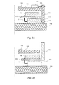
- FIG. 3A is a cross-sectional view of the power conversion apparatus 50 taken along the line IIIA-IIIA in FIG. 2A .
- FIG. 3B is a cross-sectional view of the power conversion apparatus 50 taken along the line IIIB-IIIB in FIG. 2A .
- the power conversion apparatus 50 includes a cooler 100 as a base section having a cylindrical shape and a flat top on the upper surface, and individual members stacked and arranged on the top side of the cooler 100.
- the power conversion apparatus 50 is arranged on, for example, one end side in an axial direction of the driving motor M having a cylindrical shape in the same manner.
- the cooler 100 and other members are not necessarily required to have a circular outer periphery shape and may have a polygonal outer periphery shape.
- the power module 110 is a module package including the power semiconductor 31, the diode 32, and the like encapsulated in the same package. In this embodiment, ten power modules 110 are placed on the top of the cooler 100.
- the power module 110 includes PN terminals 111 for receiving high voltage DC power supply, an AC terminal 112 for outputting AC high frequency power, and a plurality of control signal terminals 113 connected to a control substrate 150 described later.
- the power module 110 is placed on the top of the cooler 100 so that the PN terminals 111 face an inner circumferential side while the AC terminal 112 and the control signal terminals 113 face an outer circumferential side.
- the AC terminal 112 is provided with an AC bus bar 114 directed toward the outer circumferential side of the cooler 100 and extending upward of the cooler 100.
- the AC bus bar 114 is electrically connected to the driving motor M.
- the DC bus bar 120 On the upper side of the power module 110, there is arranged a DC bus bar 120 for supplying DC power to the power module 110.
- the DC bus bar 120 has an annular shape along the shape of the top of the cooler 100.
- the DC bus bar 120 includes a positive electrode and a negative electrode. The positive electrode and the negative electrode are respectively connected to the PN terminals of the power module 110.
- a set of pins 121 and 122 are arranged at two positions of the DC bus bar 120 on the outside in the circumferential direction so as to extend upward and be connected to the positive electrode and the negative electrode.
- a plurality of the smoothing capacitors 40 are placed at a predetermined interval in the circumferential direction. Each of the smoothing capacitors 40 is electrically connected to the positive electrode and the negative electrode of the DC bus bar 120.
- a first substrate 130 having substantially the same annular shape as the DC bus bar 120.
- light electrical components such as a current sensor 131 and a pad 132 are mounted so as to form a light electrical substrate. Cutout portions 135 and 136 are formed in the first substrate 130 so as to avoid contact with the pins 121 and 122 extending upward of the DC bus bar 120.
- a circular hollow portion 120a is formed in the inner circumferential side of the DC bus bar 120 and the first substrate 130.
- the current sensor 131 detects current output from the AC bus bar 114 of the power module 110.
- the current sensor 131 is formed of a Hall element, for example, and detects current of the AC bus bar 114 based on magnetic flux change of the AC bus bar 114 extending upward.
- the pad 132 is arranged in an annular shape on the inner circumferential side of the first substrate 130 and works as a connecting portion for connecting to a connection wiring electrically connected to the driving motor M (not shown).
- the pad 132 is electrically connected to a controller of the driving motor M via a cable, for example, so as to input thereto values of power to be input to the driving motor M, a rotation speed, temperature, and the like.
- control substrate 150 On the outer circumferential side of each of the plurality of power modules 110 placed on the cooler 100, the control substrate 150 (second substrate) is arranged.
- the control substrate 150 includes the control circuit 10 and controls operation of the power semiconductor 31 of the power module 110.
- the control substrate 150 is arranged in the vertical direction from the top of the cooler 100.
- the lower side of the control substrate 150 is connected to the control signal terminals 113 of the power module 110.
- the upper side of the control substrate 150 is connected to signal terminals 133 of the first substrate 130. Therefore, the lower side of the control substrate 150 is supported by the control signal terminals 113 of the power module 110, and the upper side of the control substrate 150 is supported by the signal terminals 133 of the first substrate 130.
- the power conversion apparatus 50 includes the power module 110 placed on the upper surface of the cooler 100 serving as the base section. On the upper side of the power module 110, the DC bus bar 120 and the first substrate 130 serving as the light electrical substrate are sequentially stacked. Further, the control substrate 150 is fixed and electrically connected to the power modules 110 and the first substrate 130.
- control substrate 150 is fixed at two positions on the upper and lower sides of the power module 110 and the first substrate 130, and therefore durability reliability of the control substrate 150 against external stress such as vibration or impact can be improved.
- control substrate 150 is arranged perpendicularly to the arranging direction of the power modules 110 including the power semiconductor 31, and hence influence of noise or heat of the power modules 110 can be suppressed.
- the first substrate 130 serving as the light electrical substrate on which the light electrical devices such as the current sensor 131 and the pad 132 are mounted is separated from the power module 110 and the control substrate 150, and hence influence of noise or heat on the light electrical devices can be suppressed.
- the smoothing capacitor 40 mounted on the DC bus bar 120 is arranged between the power module 110 and the first substrate 130 serving as the light electrical substrate, and therefore influence of noise or heat on the light electrical devices can be suppressed.
- the pad 132 connected to a signal line for sending and receiving a signal to and from the driving motor M is arranged on the inner circumferential side of the first substrate 130, and the AC bus bar 114 from which a high frequency high voltage of the power module 110 is output is arranged on the outer circumferential side of the first substrate 130.
- the AC bus bar 114 from which a high frequency high voltage of the power module 110 is output is arranged on the outer circumferential side of the first substrate 130.
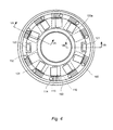
- FIG. 4 , FIG. 5A, and FIG. 5B are explanatory diagrams of the power conversion apparatus 50 according to the second embodiment of this invention.
- FIG. 4 is a top view of the power conversion apparatus 50.
- FIG. 5A is a cross-sectional view of the power conversion apparatus 50 taken along the line VA-VA in FIG. 4 .
- FIG. 5B is a cross-sectional view of the power conversion apparatus 50 taken along the line VB-VB in FIG. 4 .
- a basic structure of the second embodiment is the same as that of the first embodiment, and the same element as in the first embodiment is denoted by the same reference symbol so that overlapping description is omitted.
- control substrate 150 on which the control circuit 10 is mounted is formed of a flexible substrate, and the control substrate 150 is arranged on the outer circumferential side of the power module 110 and the first substrate 130 in a cylindrical manner.
- control substrate 150 in the power conversion apparatus 50, the control substrate 150 can be formed into an integral shape and is fixed at two positions on the upper and lower sides of the power module 110 and the first substrate 130. Therefore, durability reliability of the control substrate 150 against external stress such as vibration or impact can be improved.
- FIG. 6 , FIG. 7A, and FIG. 7B are explanatory diagrams of the power conversion apparatus 50 according to the third embodiment of this invention.
- FIG. 6 is a top view of the power conversion apparatus 50.
- FIG. 7A is a cross-sectional view of the power conversion apparatus 50 taken along the line VIIA-VIIA in FIG. 6 .
- FIG. 7B is a cross-sectional view of the power conversion apparatus 50 taken along the line VIIB-VIIB in FIG. 6 .
- a basic structure of the third embodiment is the same as that of the first embodiment, and the same element as in the first or second embodiment is denoted by the same reference symbol so that overlapping description is omitted.
- the current sensor 131 for detecting current of the AC bus bar 114 is mounted on the control substrate 150 on which the control circuit 10 is mounted.
- the current sensor 131 for detecting current of the AC bus bar 114 is mounted on the control substrate 150 side, and hence the AC bus bar 114 and the current sensor 131 can be arranged closer to each other. Therefore, it is possible to prevent a detection value from being varied due to influence of vibration or the like.
- the AC bus bar 114 and the first substrate 130 serving as the light electrical substrate can be separated from each other, and hence the first substrate 130 is hardly affected by the high frequency high voltage of the AC bus bar 114.
- FIG. 8 , FIG. 9A, and FIG. 9B are explanatory diagrams of the power conversion apparatus 50 according to the fourth embodiment of this invention.
- FIG. 8 is a top view of the power conversion apparatus 50.
- FIG. 9A is a cross-sectional view of the power conversion apparatus 50 taken along the line IXA-IXA in FIG. 8 .
- FIG. 9B is a cross-sectional view of the power conversion apparatus 50 taken along the line IXB-IXB in FIG. 8 .
- a basic structure of the fourth embodiment is the same as that of the first embodiment, and the same element as in the first to third embodiments is denoted by the same reference symbol so that overlapping description is omitted.
- a third substrate 160 having a signal wiring for connecting signals from the current sensor 131 and the pad 132 to the control substrate 150.
- the current sensor 131 and the pad 132 are mounted on the first substrate 130, the signal lines thereof are wired on the third substrate 160, and a signal terminal 161 connected to the third substrate 160 is connected to the control substrate 150.
- the first substrate 130 serving as the light electrical substrate and the control substrate serving as a heavy electrical substrate can be separated from each other via the third substrate 160. Therefore, influence of noise due to the control substrate 150 on the light electrical devices can be suppressed.
- the third substrate 160 is interposed between the power module 110 and the first substrate 130. Therefore, influence of noise or heat of the power module 110 on the light electrical devices mounted on the first substrate 130 can be suppressed.
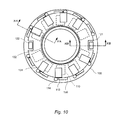
- FIG. 10 , FIG. 11A, and FIG. 11B are explanatory diagrams of the power conversion apparatus 50 according to the fifth embodiment of this invention.
- FIG. 10 is a top view of the power conversion apparatus 50.
- FIG. 11A is a cross-sectional view of the power conversion apparatus 50 taken along the line XIA-XIA in FIG. 10 .
- FIG. 11B is a cross-sectional view of the power conversion apparatus 50 taken along the line XIB-XIB in FIG. 10 .
- a basic structure of the fifth embodiment is the same as that of the first embodiment, and the same element as in the first to fourth embodiments is denoted by the same reference symbol so that overlapping description is omitted.
- the fifth embodiment is a modified example of the fourth embodiment described above, and has a structure in which the current sensor 131 is mounted on the first substrate 130 and the pad 132 is mounted on the third substrate 160.
- the current sensor 131 that may be easily affected by noise or heat in particular can be separated from the control substrate 150.
- the third substrate 160 is interposed between the power module 110 and the first substrate 130 in addition to the smoothing capacitor 40, and hence influence of noise or heat of the power module 110 on the current sensor 131 mounted on the first substrate 130 can be suppressed.
- the position of the pad 132 can be changed, and hence connectivity to the driving motor M can be improved.
- FIG. 12 , FIG. 13A, and FIG. 13B are explanatory diagrams of the power conversion apparatus 50 according to the sixth embodiment of this invention.
- FIG. 12 is a top view of the power conversion apparatus 50.
- FIG. 13A is a cross-sectional view of the power conversion apparatus 50 taken along the line XIIIA-XIIIA in FIG. 12 .
- FIG. 13B is a cross-sectional view of the power conversion apparatus 50 taken along the line XIIIB-XIIIB in FIG. 12 .
- a basic structure of the sixth embodiment is the same as that of the first embodiment, and the same element as in the first to fifth embodiments is denoted by the same reference symbol so that overlapping description is omitted.
- the sixth embodiment is a modified example of the fourth and fifth embodiments described above, and has a structure in which the current sensor 131 is mounted on the first substrate 130, and a first pad 132A and a second pad 132B are mounted on the first substrate 130 and the third substrate 160, respectively.
- the different pads 132 are arranged on the plurality of substrates in this way, and hence the degree of freedom of wiring the signal line is improved, and connectivity to the driving motor M can be improved.
- FIG. 14 , FIG. 15A, and FIG. 15B are explanatory diagrams of the power conversion apparatus 50 according to the seventh embodiment of this invention.
- FIG. 14 is a top view of the power conversion apparatus 50.
- FIG. 15A is a cross-sectional view of the power conversion apparatus 50 taken along the line XVA-XVA in FIG. 14 .
- FIG. 15B is a cross-sectional view of the power conversion apparatus 50 taken along the line XVB-XVB in FIG. 14 .
- a basic structure of the seventh embodiment is the same as that of the first embodiment, and the same element as in the first to sixth embodiments is denoted by the same reference symbol so that overlapping description is omitted.
- the seventh embodiment is different from the first to sixth embodiments described above in that the power module 110 is placed on the upper surface of the cooler 100 so that the AC bus bar 114 and the control signal terminals 113 are on the inner circumferential side while the PN terminals 111 are on the outer circumferential side.
- Ten power modules 110 are placed along the circular shape of the top of the cooler 100 at a predetermined interval along the circumferential direction.
- the control substrates 150 are respectively arranged correspondingly to positions of the power modules 110 on the inner circumferential side of the circle on which the power modules 110 are arranged.
- the DC bus bar 120 is arranged on the upper side of the power module 110, and the pins 121 and 122 are arranged to extend upward at two positions on the inner circumferential side of the annular DC bus bar 120.
- the first substrate 130 is arranged on the upper side of the DC bus bar 120, and the cutout portions 135 and 136 for avoiding contact with the pins 121 and 122 of the DC bus bar 120 are formed at two positions on the inner circumferential side of the first substrate 130.
- the pad 132 arranged on the first substrate 130 is arranged in an annular shape on the outer circumferential side of the first substrate 130.
- the AC bus bar 114 extending upward from the power module 110 extends upward from the circular hollow portion 120a on the inner circumferential side of the DC bus bar 120 and the first substrate 130.
- the pins 121 and 122 of the DC bus bar 120 also extend upward from the circular hollow portion 120a on the inner circumferential side of the DC bus bar 120 and the first substrate 130.
- the lower side of the control substrate 150 is fixed to the control signal terminals 113 of the power module 110 while the upper side of the control substrate 150 is fixed to the signal terminals 133 of the first substrate 130.
- the AC bus bar 114 and the DC bus bar 120 extend upward from the inner circumferential side, while the pad 132 connected to the signal line of the driving motor M is arranged on the outer circumferential side.
- the degree of freedom of wiring the signal line connected to the DC bus bar 120, the AC bus bar 114, and the pad 132 is improved, and connectivity to the driving motor M can be improved.
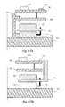
- FIG. 16 , FIG. 17A, and FIG. 17B are explanatory diagrams of the power conversion apparatus 50 according to the eighth embodiment of this invention.
- FIG. 16 is a top view of the power conversion apparatus 50.
- FIG. 17A is a cross-sectional view of the power conversion apparatus 50 taken along the line XVIIA-XVIIA in FIG. 16 .
- FIG. 17B is a cross-sectional view of the power conversion apparatus 50 taken along the line XVIIB-XVIIB in FIG. 16 .
- a basic structure of the eighth embodiment is the same as that of the first embodiment, and the same element as in the first to seventh embodiments is denoted by the same reference symbol so that overlapping description is omitted.
- the eighth embodiment is a modified example of the seventh embodiment described above.
- the control substrates 150 are arranged on the inner circumferential side of the circle on which the power modules 110 are arranged, and the AC bus bar 114 is arranged to extend upward on the inner circumferential side.
- the third substrate 160 is further arranged for connecting the signals of the current sensor 131 and the pad 132 to the control substrate 150.
- the control substrate 150 is arranged along the circular hollow portion 120a on the inner circumferential side of the DC bus bar 120 and the first substrate 130 so that the lower side thereof is fixed to the control signal terminals 113 of the power module 110 while the upper side thereof is fixed to the third substrate 160.
- the pins 121 and 122 of the DC bus bar 120 and the cutout portions 134 and 135 of the first substrate 130 are arranged on the outer circumferential side but may be arranged on the inner circumferential side as in the seventh embodiment described above.
- the third substrate 160 is provided besides the first substrate 130 in this way, the effect similar to that of the fourth embodiment can be obtained in addition to the effect of the seventh embodiment described above.
- FIG. 18 , FIG. 19A, and FIG. 19B are explanatory diagrams of the power conversion apparatus 50 according to the ninth embodiment of this invention.
- FIG. 18 is a top view of the power conversion apparatus 50.
- FIG. 19A is a cross-sectional view of the power conversion apparatus 50 taken along the line XIXA-XIXA in FIG. 18 .
- FIG. 19B is a cross-sectional view of the power conversion apparatus 50 taken along the line XIXB-XIXIB in FIG. 18 .
- a basic structure of the ninth embodiment is the same as that of the first embodiment, and the same element as in the first to eighth embodiments is denoted by the same reference symbol so that overlapping description is omitted.
- the ninth embodiment is a modified example of the seventh embodiment.
- the power modules 110 are placed on the upper surface of the cooler 100 so as to have different directions alternately.
- the power module 110 whose AC bus bar 114 and control signal terminals 113 are on the inner circumferential side and the power modules 110 whose AC bus bar 114 and control signal terminals 113 are on the outer circumferential side are arranged alternately.
- pins 121 and 122 of the DC bus bar 120 and the cutout portions 134 and 135 of the first substrate 130 are arranged on the outer circumferential side in the ninth embodiment but may be arranged on the inner circumferential side as in the seventh embodiment described above.
- the AC bus bar 114 extends upward from the inner circumferential side in this way.
- the degree of freedom of wiring the signal line or the like connected to the DC bus bar 120, the AC bus bar 114, and the pad 132 is improved, and hence connectivity to the driving motor M can be improved.
- the power conversion apparatus 50 including the power semiconductor 31 and the diode 32 so as to form the inverter, but this structure is not a limitation.
- the embodiments described above can be applied similarly to a semiconductor device including a semiconductor element, and a control substrate and a light electrical substrate relating to operation of the semiconductor element.
- control substrate 150 may be formed of a flexible substrate having flexibility.
Landscapes
- Engineering & Computer Science (AREA)
- Power Engineering (AREA)
- Microelectronics & Electronic Packaging (AREA)
- Inverter Devices (AREA)
- Physics & Mathematics (AREA)
- Thermal Sciences (AREA)
Abstract

Description
- This invention relates to a power conversion apparatus for converting electricity by a semiconductor element.
- A power conversion apparatus, which is used for inverter control of an electric motor or the like, includes a power semiconductor such as a switching element, and a control circuit for controlling operation of the power semiconductor device. The power semiconductor generates much heat, and hence it is necessary to construct so that the control circuit is free from being affected by the heat.
- As the power conversion apparatus described above,
JP4609504B - In the power conversion apparatus having the structure described in
JP 4609504 B - The present invention was developed in view of such a problem and aims to provide a power conversion apparatus including a power semiconductor element in which durability can be improved.
- One aspect of the present invention is applied to a power conversion apparatus, including: a power module including a power semiconductor; a base section including a cooler for cooling the power module; a control substrate, on which a control circuit for controlling the power module is mounted; a first bus bar for supplying power to the power module; a second bus bar for outputting power from the power module; a smoothing capacitor for smoothing power of the first bus bar; and a first substrate including a signal wiring.
- Embodiments and advantages of the present invention are described in detail below with reference to the accompanying drawings.
-
-
FIG. 1 is an explanatory diagram of a drive system including a semiconductor module according to a first embodiment of this invention. -
FIG. 2A is an explanatory diagram of a power conversion apparatus according to the first embodiment of this invention. -
FIG. 2B is an explanatory diagram of the power conversion apparatus according to the first embodiment of this invention. -
FIG. 3A is an explanatory diagram of the power conversion apparatus according to the first embodiment of this invention and is a cross-sectional view ofFIG. 2A . -
FIG. 3B is an explanatory diagram of the power conversion apparatus according to the first embodiment of this invention and is a cross-sectional view ofFIG. 2A . -
FIG. 4 is an explanatory diagram of a power conversion apparatus according to a second embodiment of this invention. -
FIG. 5A is an explanatory diagram of the power conversion apparatus according to the second embodiment of this invention and is a cross-sectional view ofFIG. 4 . -
FIG. 5B is an explanatory diagram of the power conversion apparatus according to the second embodiment of this invention and is a cross-sectional view ofFIG. 4 . -
FIG. 6 is an explanatory diagram of a power conversion apparatus according to a third embodiment of this invention. -
FIG. 7A is an explanatory diagram of the power conversion apparatus according to the third embodiment of this invention and is a cross-sectional view ofFIG. 6 . -
FIG. 7B is an explanatory diagram of the power conversion apparatus according to the third embodiment of this invention and is a cross-sectional view ofFIG. 6 . -
FIG. 8 is an explanatory diagram of a power conversion apparatus according to a fourth embodiment of this invention. -
FIG. 9A is an explanatory diagram of the power conversion apparatus according to the fourth embodiment of this invention and is a cross-sectional view ofFIG. 8 . -
FIG. 9B is an explanatory diagram of the power conversion apparatus according to the fourth embodiment of this invention and is a cross-sectional view ofFIG. 8 . -
FIG. 10 is an explanatory diagram of a power conversion apparatus according to a fifth embodiment of this invention. -
FIG. 11A is an explanatory diagram of the power conversion apparatus according to the fifth embodiment of this invention and is a cross-sectional view ofFIG. 10 . -
FIG. 11B is an explanatory diagram of the power conversion apparatus according to the fifth embodiment of this invention and is a cross-sectional view ofFIG. 10 . -
FIG. 12 is an explanatory diagram of a power conversion apparatus according to a sixth embodiment of this invention. -
FIG. 13A is an explanatory diagram of the power conversion apparatus according to the sixth embodiment of this invention and is a cross-sectional view ofFIG. 12 . -
FIG. 13B is an explanatory diagram of the power conversion apparatus according to the sixth embodiment of this invention and is a cross-sectional view ofFIG. 12 . -
FIG. 14 is an explanatory diagram of a power conversion apparatus according to a seventh embodiment of this invention. -
FIG. 15A is an explanatory diagram of the power conversion apparatus according to the seventh embodiment of this invention and is a cross-sectional view ofFIG. 14 . -
FIG. 15B is an explanatory diagram of the power conversion apparatus according to the seventh embodiment of this invention and is a cross-sectional view ofFIG. 14 . -
FIG. 16 is an explanatory diagram of a power conversion apparatus according to an eighth embodiment of this invention. -
FIG. 17A is an explanatory diagram of the power conversion apparatus according to the eighth embodiment of this invention and is a cross-sectional view ofFIG. 16 . -
FIG. 17B is an explanatory diagram of the power conversion apparatus according to the eighth embodiment of this invention and is a cross-sectional view ofFIG. 16 . -
FIG. 18 is an explanatory diagram of a power conversion apparatus according to a ninth embodiment of this invention. -
FIG. 19A is an explanatory diagram of the power conversion apparatus according to the ninth embodiment of this invention and is a cross-sectional view ofFIG. 18 . -
FIG. 19B is an explanatory diagram of the power conversion apparatus according to the ninth embodiment of this invention and is a cross-sectional view ofFIG. 18 . - Embodiments of this invention are described with reference to the drawings.
-
FIG. 1 is an explanatory diagram of adrive system 1 according to a first embodiment of this invention. - The
drive system 1 includes apower conversion apparatus 50, abattery 20, and a driving motor M. Thepower conversion apparatus 50 includes acontrol circuit 10, apower semiconductor 31, adiode 32, a smoothingcapacitor 40, and the like. Thecontrol circuit 10 controls an output of thepower semiconductor 31 so as to control the driving motor M. - The
battery 20 supplies electric power to the driving motor M and stores regenerative electric power from the driving motor M. Thebattery 20 is formed as a battery module, in which a plurality of secondary batteries, such as lead-acid batteries, nickel-hydrogen batteries, or lithium-ion batteries, are connected in series or in parallel. - The
power semiconductor 31 is formed of a semiconductor element such as an IGBT. Thediode 32 is formed of a semiconductor element such as a fast recovery diode (FRD). Thediode 32 prevents reverse current from being applied to thepower semiconductor 31 so as to protect thepower semiconductor 31. The smoothingcapacitor 40 smoothes power output from thepower semiconductor 31. - When increasing an output of the driving motor M, for example, the
control circuit 10 applies gate current to eachpower semiconductor 31. Thus, high current from thebattery 20 is supplied to the driving motor M. - The
control circuit 10 controls the gate current by a duty ratio or the like so as to control the output of the driving motor M. When the driving motor M regenerates power, the power is stored in thebattery 20 via thepower conversion apparatus 50. - Next, a structure of the
power conversion apparatus 50 according to the first embodiment of this invention is described. -
FIG. 2A, FIG. 2B ,FIG. 3A, and FIG. 3B are explanatory diagrams of thepower conversion apparatus 50 according to the first embodiment of this invention.FIG. 2A is a top view of thepower conversion apparatus 50.FIG. 2B illustrates a structure of apower module 110.FIG. 3A is a cross-sectional view of thepower conversion apparatus 50 taken along the line IIIA-IIIA inFIG. 2A .FIG. 3B is a cross-sectional view of thepower conversion apparatus 50 taken along the line IIIB-IIIB inFIG. 2A . - The
power conversion apparatus 50 includes a cooler 100 as a base section having a cylindrical shape and a flat top on the upper surface, and individual members stacked and arranged on the top side of the cooler 100. - The
power conversion apparatus 50 is arranged on, for example, one end side in an axial direction of the driving motor M having a cylindrical shape in the same manner. The cooler 100 and other members are not necessarily required to have a circular outer periphery shape and may have a polygonal outer periphery shape. - On the top of the cooler 100, a plurality of the
power modules 110 are placed along the circular shape of the top at a predetermined interval in the circumferential direction. Thepower module 110 is a module package including thepower semiconductor 31, thediode 32, and the like encapsulated in the same package. In this embodiment, tenpower modules 110 are placed on the top of the cooler 100. - The
power module 110 includesPN terminals 111 for receiving high voltage DC power supply, anAC terminal 112 for outputting AC high frequency power, and a plurality ofcontrol signal terminals 113 connected to acontrol substrate 150 described later. - The
power module 110 is placed on the top of the cooler 100 so that thePN terminals 111 face an inner circumferential side while theAC terminal 112 and thecontrol signal terminals 113 face an outer circumferential side. TheAC terminal 112 is provided with anAC bus bar 114 directed toward the outer circumferential side of the cooler 100 and extending upward of the cooler 100. TheAC bus bar 114 is electrically connected to the driving motor M. - On the upper side of the
power module 110, there is arranged aDC bus bar 120 for supplying DC power to thepower module 110. TheDC bus bar 120 has an annular shape along the shape of the top of the cooler 100. TheDC bus bar 120 includes a positive electrode and a negative electrode. The positive electrode and the negative electrode are respectively connected to the PN terminals of thepower module 110. - A set of
pins DC bus bar 120 on the outside in the circumferential direction so as to extend upward and be connected to the positive electrode and the negative electrode. - On the upper surface of the
DC bus bar 120, a plurality of the smoothingcapacitors 40 are placed at a predetermined interval in the circumferential direction. Each of the smoothingcapacitors 40 is electrically connected to the positive electrode and the negative electrode of theDC bus bar 120. - At a position further above the
DC bus bar 120, there is arranged afirst substrate 130 having substantially the same annular shape as theDC bus bar 120. On thefirst substrate 130, light electrical components such as acurrent sensor 131 and apad 132 are mounted so as to form a light electrical substrate.Cutout portions first substrate 130 so as to avoid contact with thepins DC bus bar 120. - A circular
hollow portion 120a is formed in the inner circumferential side of theDC bus bar 120 and thefirst substrate 130. - The
current sensor 131 detects current output from theAC bus bar 114 of thepower module 110. Thecurrent sensor 131 is formed of a Hall element, for example, and detects current of theAC bus bar 114 based on magnetic flux change of theAC bus bar 114 extending upward. - The
pad 132 is arranged in an annular shape on the inner circumferential side of thefirst substrate 130 and works as a connecting portion for connecting to a connection wiring electrically connected to the driving motor M (not shown). Thepad 132 is electrically connected to a controller of the driving motor M via a cable, for example, so as to input thereto values of power to be input to the driving motor M, a rotation speed, temperature, and the like. - On the outer circumferential side of each of the plurality of
power modules 110 placed on the cooler 100, the control substrate 150 (second substrate) is arranged. Thecontrol substrate 150 includes thecontrol circuit 10 and controls operation of thepower semiconductor 31 of thepower module 110. - The
control substrate 150 is arranged in the vertical direction from the top of the cooler 100. The lower side of thecontrol substrate 150 is connected to thecontrol signal terminals 113 of thepower module 110. The upper side of thecontrol substrate 150 is connected to signalterminals 133 of thefirst substrate 130. Therefore, the lower side of thecontrol substrate 150 is supported by thecontrol signal terminals 113 of thepower module 110, and the upper side of thecontrol substrate 150 is supported by thesignal terminals 133 of thefirst substrate 130. - As described above, in the first embodiment of this invention, the
power conversion apparatus 50 includes thepower module 110 placed on the upper surface of the cooler 100 serving as the base section. On the upper side of thepower module 110, theDC bus bar 120 and thefirst substrate 130 serving as the light electrical substrate are sequentially stacked. Further, thecontrol substrate 150 is fixed and electrically connected to thepower modules 110 and thefirst substrate 130. - With this structure, the
control substrate 150 is fixed at two positions on the upper and lower sides of thepower module 110 and thefirst substrate 130, and therefore durability reliability of thecontrol substrate 150 against external stress such as vibration or impact can be improved. - In addition, the
control substrate 150 is arranged perpendicularly to the arranging direction of thepower modules 110 including thepower semiconductor 31, and hence influence of noise or heat of thepower modules 110 can be suppressed. - In addition, the
first substrate 130 serving as the light electrical substrate on which the light electrical devices such as thecurrent sensor 131 and thepad 132 are mounted is separated from thepower module 110 and thecontrol substrate 150, and hence influence of noise or heat on the light electrical devices can be suppressed. - In addition, the smoothing
capacitor 40 mounted on theDC bus bar 120 is arranged between thepower module 110 and thefirst substrate 130 serving as the light electrical substrate, and therefore influence of noise or heat on the light electrical devices can be suppressed. - In addition, the
pad 132 connected to a signal line for sending and receiving a signal to and from the driving motor M is arranged on the inner circumferential side of thefirst substrate 130, and theAC bus bar 114 from which a high frequency high voltage of thepower module 110 is output is arranged on the outer circumferential side of thefirst substrate 130. With this structure, influence of noise or heat of theAC bus bar 114 on the signal line can be suppressed. Further, signal lines can be arranged in a concentrated manner on the upper side of thepower conversion apparatus 50, and hence workability in connection to the driving motor M can be improved. - Next, a
power conversion apparatus 50 according to a second embodiment of this invention is described. -
FIG. 4 ,FIG. 5A, and FIG. 5B are explanatory diagrams of thepower conversion apparatus 50 according to the second embodiment of this invention.FIG. 4 is a top view of thepower conversion apparatus 50.FIG. 5A is a cross-sectional view of thepower conversion apparatus 50 taken along the line VA-VA inFIG. 4 .FIG. 5B is a cross-sectional view of thepower conversion apparatus 50 taken along the line VB-VB inFIG. 4 . - Further, a basic structure of the second embodiment is the same as that of the first embodiment, and the same element as in the first embodiment is denoted by the same reference symbol so that overlapping description is omitted.
- In the second embodiment, the
control substrate 150 on which thecontrol circuit 10 is mounted is formed of a flexible substrate, and thecontrol substrate 150 is arranged on the outer circumferential side of thepower module 110 and thefirst substrate 130 in a cylindrical manner. - With this structure, in the
power conversion apparatus 50, thecontrol substrate 150 can be formed into an integral shape and is fixed at two positions on the upper and lower sides of thepower module 110 and thefirst substrate 130. Therefore, durability reliability of thecontrol substrate 150 against external stress such as vibration or impact can be improved. - Next, a
power conversion apparatus 50 according to a third embodiment of this invention is described. -
FIG. 6 ,FIG. 7A, and FIG. 7B are explanatory diagrams of thepower conversion apparatus 50 according to the third embodiment of this invention.FIG. 6 is a top view of thepower conversion apparatus 50.FIG. 7A is a cross-sectional view of thepower conversion apparatus 50 taken along the line VIIA-VIIA inFIG. 6 .FIG. 7B is a cross-sectional view of thepower conversion apparatus 50 taken along the line VIIB-VIIB inFIG. 6 . - Further, a basic structure of the third embodiment is the same as that of the first embodiment, and the same element as in the first or second embodiment is denoted by the same reference symbol so that overlapping description is omitted.
- In the third embodiment, the
current sensor 131 for detecting current of theAC bus bar 114 is mounted on thecontrol substrate 150 on which thecontrol circuit 10 is mounted. - In this way, in the third embodiment of this invention, the
current sensor 131 for detecting current of theAC bus bar 114 is mounted on thecontrol substrate 150 side, and hence theAC bus bar 114 and thecurrent sensor 131 can be arranged closer to each other. Therefore, it is possible to prevent a detection value from being varied due to influence of vibration or the like. - In addition, the
AC bus bar 114 and thefirst substrate 130 serving as the light electrical substrate can be separated from each other, and hence thefirst substrate 130 is hardly affected by the high frequency high voltage of theAC bus bar 114. - Next, a
power conversion apparatus 50 according to a fourth embodiment of this invention is described. -
FIG. 8 ,FIG. 9A, and FIG. 9B are explanatory diagrams of thepower conversion apparatus 50 according to the fourth embodiment of this invention.FIG. 8 is a top view of thepower conversion apparatus 50.FIG. 9A is a cross-sectional view of thepower conversion apparatus 50 taken along the line IXA-IXA inFIG. 8 .FIG. 9B is a cross-sectional view of thepower conversion apparatus 50 taken along the line IXB-IXB inFIG. 8 . - Further, a basic structure of the fourth embodiment is the same as that of the first embodiment, and the same element as in the first to third embodiments is denoted by the same reference symbol so that overlapping description is omitted.
- In the fourth embodiment, in addition to the
substrate 130 on which thecurrent sensor 131 and thepad 132 are mounted, there is further arranged athird substrate 160 having a signal wiring for connecting signals from thecurrent sensor 131 and thepad 132 to thecontrol substrate 150. - More specifically, the
current sensor 131 and thepad 132 are mounted on thefirst substrate 130, the signal lines thereof are wired on thethird substrate 160, and asignal terminal 161 connected to thethird substrate 160 is connected to thecontrol substrate 150. - In the fourth embodiment, in this way, the
first substrate 130 serving as the light electrical substrate and the control substrate serving as a heavy electrical substrate can be separated from each other via thethird substrate 160. Therefore, influence of noise due to thecontrol substrate 150 on the light electrical devices can be suppressed. - In addition, besides the smoothing
capacitor 40, thethird substrate 160 is interposed between thepower module 110 and thefirst substrate 130. Therefore, influence of noise or heat of thepower module 110 on the light electrical devices mounted on thefirst substrate 130 can be suppressed. - Next, a
power conversion apparatus 50 according to a fifth embodiment of this invention is described. -
FIG. 10 ,FIG. 11A, and FIG. 11B are explanatory diagrams of thepower conversion apparatus 50 according to the fifth embodiment of this invention.FIG. 10 is a top view of thepower conversion apparatus 50.FIG. 11A is a cross-sectional view of thepower conversion apparatus 50 taken along the line XIA-XIA inFIG. 10 .FIG. 11B is a cross-sectional view of thepower conversion apparatus 50 taken along the line XIB-XIB inFIG. 10 . - Further, a basic structure of the fifth embodiment is the same as that of the first embodiment, and the same element as in the first to fourth embodiments is denoted by the same reference symbol so that overlapping description is omitted.
- The fifth embodiment is a modified example of the fourth embodiment described above, and has a structure in which the
current sensor 131 is mounted on thefirst substrate 130 and thepad 132 is mounted on thethird substrate 160. - In the fifth embodiment, with this structure, the
current sensor 131 that may be easily affected by noise or heat in particular can be separated from thecontrol substrate 150. Further, thethird substrate 160 is interposed between thepower module 110 and thefirst substrate 130 in addition to the smoothingcapacitor 40, and hence influence of noise or heat of thepower module 110 on thecurrent sensor 131 mounted on thefirst substrate 130 can be suppressed. - In addition, the position of the
pad 132 can be changed, and hence connectivity to the driving motor M can be improved. - Next, a
power conversion apparatus 50 according to a sixth embodiment of this invention is described. -
FIG. 12 ,FIG. 13A, and FIG. 13B are explanatory diagrams of thepower conversion apparatus 50 according to the sixth embodiment of this invention.FIG. 12 is a top view of thepower conversion apparatus 50.FIG. 13A is a cross-sectional view of thepower conversion apparatus 50 taken along the line XIIIA-XIIIA inFIG. 12 .FIG. 13B is a cross-sectional view of thepower conversion apparatus 50 taken along the line XIIIB-XIIIB inFIG. 12 . - Further, a basic structure of the sixth embodiment is the same as that of the first embodiment, and the same element as in the first to fifth embodiments is denoted by the same reference symbol so that overlapping description is omitted.
- The sixth embodiment is a modified example of the fourth and fifth embodiments described above, and has a structure in which the
current sensor 131 is mounted on thefirst substrate 130, and afirst pad 132A and asecond pad 132B are mounted on thefirst substrate 130 and thethird substrate 160, respectively. - In the sixth embodiment, the
different pads 132 are arranged on the plurality of substrates in this way, and hence the degree of freedom of wiring the signal line is improved, and connectivity to the driving motor M can be improved. - Next, a
power conversion apparatus 50 according to a seventh embodiment of this invention is described. -
FIG. 14 ,FIG. 15A, and FIG. 15B are explanatory diagrams of thepower conversion apparatus 50 according to the seventh embodiment of this invention.FIG. 14 is a top view of thepower conversion apparatus 50.FIG. 15A is a cross-sectional view of thepower conversion apparatus 50 taken along the line XVA-XVA inFIG. 14 .FIG. 15B is a cross-sectional view of thepower conversion apparatus 50 taken along the line XVB-XVB inFIG. 14 . - Further, a basic structure of the seventh embodiment is the same as that of the first embodiment, and the same element as in the first to sixth embodiments is denoted by the same reference symbol so that overlapping description is omitted.
- The seventh embodiment is different from the first to sixth embodiments described above in that the
power module 110 is placed on the upper surface of the cooler 100 so that theAC bus bar 114 and thecontrol signal terminals 113 are on the inner circumferential side while thePN terminals 111 are on the outer circumferential side. Tenpower modules 110 are placed along the circular shape of the top of the cooler 100 at a predetermined interval along the circumferential direction. - The
control substrates 150 are respectively arranged correspondingly to positions of thepower modules 110 on the inner circumferential side of the circle on which thepower modules 110 are arranged. - The
DC bus bar 120 is arranged on the upper side of thepower module 110, and thepins DC bus bar 120. - The
first substrate 130 is arranged on the upper side of theDC bus bar 120, and thecutout portions pins DC bus bar 120 are formed at two positions on the inner circumferential side of thefirst substrate 130. Thepad 132 arranged on thefirst substrate 130 is arranged in an annular shape on the outer circumferential side of thefirst substrate 130. - The
AC bus bar 114 extending upward from thepower module 110 extends upward from the circularhollow portion 120a on the inner circumferential side of theDC bus bar 120 and thefirst substrate 130. Similarly, thepins DC bus bar 120 also extend upward from the circularhollow portion 120a on the inner circumferential side of theDC bus bar 120 and thefirst substrate 130. - Along this
hollow portion 120a, the lower side of thecontrol substrate 150 is fixed to thecontrol signal terminals 113 of thepower module 110 while the upper side of thecontrol substrate 150 is fixed to thesignal terminals 133 of thefirst substrate 130. - In the seventh embodiment, in this way, the
AC bus bar 114 and theDC bus bar 120 extend upward from the inner circumferential side, while thepad 132 connected to the signal line of the driving motor M is arranged on the outer circumferential side. With this structure, the degree of freedom of wiring the signal line connected to theDC bus bar 120, theAC bus bar 114, and thepad 132 is improved, and connectivity to the driving motor M can be improved. - Next, a
power conversion apparatus 50 according to an eighth embodiment of this invention is described. -
FIG. 16 ,FIG. 17A, and FIG. 17B are explanatory diagrams of thepower conversion apparatus 50 according to the eighth embodiment of this invention.FIG. 16 is a top view of thepower conversion apparatus 50.FIG. 17A is a cross-sectional view of thepower conversion apparatus 50 taken along the line XVIIA-XVIIA inFIG. 16 .FIG. 17B is a cross-sectional view of thepower conversion apparatus 50 taken along the line XVIIB-XVIIB inFIG. 16 . - Further, a basic structure of the eighth embodiment is the same as that of the first embodiment, and the same element as in the first to seventh embodiments is denoted by the same reference symbol so that overlapping description is omitted.
- The eighth embodiment is a modified example of the seventh embodiment described above. The
control substrates 150 are arranged on the inner circumferential side of the circle on which thepower modules 110 are arranged, and theAC bus bar 114 is arranged to extend upward on the inner circumferential side. - Further, in the eighth embodiment, similarly to the fourth embodiment described above, in addition to the
substrate 130 on which thecurrent sensor 131 and thepad 132 are mounted, thethird substrate 160 is further arranged for connecting the signals of thecurrent sensor 131 and thepad 132 to thecontrol substrate 150. - The
control substrate 150 is arranged along the circularhollow portion 120a on the inner circumferential side of theDC bus bar 120 and thefirst substrate 130 so that the lower side thereof is fixed to thecontrol signal terminals 113 of thepower module 110 while the upper side thereof is fixed to thethird substrate 160. - In the eighth embodiment, the
pins DC bus bar 120 and thecutout portions first substrate 130 are arranged on the outer circumferential side but may be arranged on the inner circumferential side as in the seventh embodiment described above. - In the eighth embodiment, because the
third substrate 160 is provided besides thefirst substrate 130 in this way, the effect similar to that of the fourth embodiment can be obtained in addition to the effect of the seventh embodiment described above. - Next, a
power conversion apparatus 50 according to a ninth embodiment of this invention is described. -
FIG. 18 ,FIG. 19A, and FIG. 19B are explanatory diagrams of thepower conversion apparatus 50 according to the ninth embodiment of this invention.FIG. 18 is a top view of thepower conversion apparatus 50.FIG. 19A is a cross-sectional view of thepower conversion apparatus 50 taken along the line XIXA-XIXA inFIG. 18 .FIG. 19B is a cross-sectional view of thepower conversion apparatus 50 taken along the line XIXB-XIXIB inFIG. 18 . - Further, a basic structure of the ninth embodiment is the same as that of the first embodiment, and the same element as in the first to eighth embodiments is denoted by the same reference symbol so that overlapping description is omitted.
- The ninth embodiment is a modified example of the seventh embodiment. The
power modules 110 are placed on the upper surface of the cooler 100 so as to have different directions alternately. In other words, thepower module 110 whoseAC bus bar 114 andcontrol signal terminals 113 are on the inner circumferential side and thepower modules 110 whoseAC bus bar 114 andcontrol signal terminals 113 are on the outer circumferential side are arranged alternately. - Further, the
pins DC bus bar 120 and thecutout portions first substrate 130 are arranged on the outer circumferential side in the ninth embodiment but may be arranged on the inner circumferential side as in the seventh embodiment described above. - In the ninth embodiment, the
AC bus bar 114 extends upward from the inner circumferential side in this way. With this structure, the degree of freedom of wiring the signal line or the like connected to theDC bus bar 120, theAC bus bar 114, and thepad 132 is improved, and hence connectivity to the driving motor M can be improved. - Further, the embodiments of this invention described above are merely examples of the structure embodying this invention, and this structure is not intended to be interpreted as a limitation. In addition, the structures of the first to ninth embodiments may be combined.
- In addition, in the embodiments of this invention, description has been given of the
power conversion apparatus 50 including thepower semiconductor 31 and thediode 32 so as to form the inverter, but this structure is not a limitation. The embodiments described above can be applied similarly to a semiconductor device including a semiconductor element, and a control substrate and a light electrical substrate relating to operation of the semiconductor element. - In addition, in the embodiments of this invention described above, the
control substrate 150 may be formed of a flexible substrate having flexibility. - Though a description has been given of the embodiments of this invention, the embodiments describe only a part of application examples of this invention, and are not intended to limit the technical scope of this invention to the specific configurations of the above-mentioned embodiments.
- This application claims priority from Japanese Patent Application No.
2012-50627 - Exclusive nature or features of the embodiments of this invention are claimed as follows.
Claims (4)
- A power conversion apparatus, comprising:a power module including a power semiconductor;a base section including a cooler adapted to cool the power module;a second substrate, on which a control circuit adapted to control the power module is mounted;a first bus bar adapted to supply power to the power module;a second bus bar adapted to output power from the power module;a smoothing capacitor adapted to smooth power of the first bus bar; anda first substrate including a signal wiring,wherein the power module is placed on an upper surface of the base section,wherein the first bus bar, the smoothing capacitor, and the first substrate are sequentially stacked on an upper side of the power module, andwherein the second substrate is arranged in an upright direction with respect to the base section and is fixed to the power module and the first substrate.
- The power conversion apparatus according to claim 1, further comprising a third substrate including a current detecting portion adapted to detect a current of the second bus bar,
wherein the first bus bar includes a pin extending upward, and
wherein the third substrate has a cutout portion formed at a position corresponding to the pin. - The power conversion apparatus according to claim 1 or 2, wherein the smoothing capacitor is mounted on the first bus bar and is arranged between the power module and the first substrate.
- The power conversion apparatus according to any one of claims 1 to 3,
wherein the first substrate or the third substrate includes a connecting portion to which a signal line is connected adapted to send and receive a signal to and from an external apparatus, and
wherein the connecting portion is arranged on an outer circumferential side or an inner circumferential side of the first substrate or the third substrate.
Applications Claiming Priority (2)
| Application Number | Priority Date | Filing Date | Title |
|---|---|---|---|
| JP2012050627A JP2013187998A (en) | 2012-03-07 | 2012-03-07 | Electric power conversion system |
| PCT/JP2013/055144 WO2013133104A1 (en) | 2012-03-07 | 2013-02-27 | Power conversion apparatus |
Publications (2)
| Publication Number | Publication Date |
|---|---|
| EP2824821A1 true EP2824821A1 (en) | 2015-01-14 |
| EP2824821A4 EP2824821A4 (en) | 2015-10-21 |
Family
ID=49116586
Family Applications (1)
| Application Number | Title | Priority Date | Filing Date |
|---|---|---|---|
| EP13757512.2A Withdrawn EP2824821A4 (en) | 2012-03-07 | 2013-02-27 | Power conversion apparatus |
Country Status (5)
| Country | Link |
|---|---|
| US (1) | US20150029672A1 (en) |
| EP (1) | EP2824821A4 (en) |
| JP (1) | JP2013187998A (en) |
| CN (1) | CN104205600A (en) |
| WO (1) | WO2013133104A1 (en) |
Families Citing this family (13)
| Publication number | Priority date | Publication date | Assignee | Title |
|---|---|---|---|---|
| JP5888010B2 (en) * | 2012-03-08 | 2016-03-16 | 日産自動車株式会社 | Inverter module |
| EP2790217A1 (en) * | 2013-04-09 | 2014-10-15 | ABB Technology AG | Power semiconductor module |
| JP2015050257A (en) * | 2013-08-30 | 2015-03-16 | 株式会社東芝 | Power conversion device for vehicle and railway vehicle |
| JP6383614B2 (en) * | 2014-09-08 | 2018-08-29 | 京セラ株式会社 | Capacitor module and power unit |
| JP6137421B2 (en) * | 2014-12-24 | 2017-05-31 | 日本精工株式会社 | Power semiconductor module and electric power steering apparatus using the same |
| JP6455154B2 (en) * | 2015-01-08 | 2019-01-23 | 株式会社デンソー | Vehicle electronics |
| DE102015113503A1 (en) * | 2015-08-14 | 2017-02-16 | Schweizer Electronic Ag | Electronic switching element and modular power converter |
| DE102015219867A1 (en) * | 2015-10-13 | 2017-04-13 | Lenze Drives Gmbh | Circuit board, B-end shield, engine kit and electric motor |
| JP6098705B1 (en) * | 2015-12-28 | 2017-03-22 | ダイキン工業株式会社 | Inverter |
| CN108966681B (en) * | 2016-03-02 | 2020-09-08 | 三菱电机株式会社 | Power conversion device |
| JP6143980B1 (en) * | 2016-03-02 | 2017-06-07 | 三菱電機株式会社 | Power converter |
| JP7239380B2 (en) * | 2019-04-16 | 2023-03-14 | 株式会社日立製作所 | power converter |
| CN114846600A (en) * | 2019-12-28 | 2022-08-02 | 丹佛斯硅动力有限责任公司 | Power module with improved electrical and thermal properties |
Family Cites Families (13)
| Publication number | Priority date | Publication date | Assignee | Title |
|---|---|---|---|---|
| US5907475A (en) * | 1996-04-16 | 1999-05-25 | Allen-Bradley Company, Llc | Circuit board system having a mounted board and a plurality of mounting boards |
| JP3949368B2 (en) * | 2000-10-17 | 2007-07-25 | 三菱電機株式会社 | AC generator for vehicles |
| WO2007080748A1 (en) * | 2006-01-16 | 2007-07-19 | Mitsubishi Electric Corporation | Drive circuit of motor and outdoor unit of air conditioner |
| JP4434181B2 (en) * | 2006-07-21 | 2010-03-17 | 株式会社日立製作所 | Power converter |
| US8008805B2 (en) * | 2006-12-07 | 2011-08-30 | Nissan Motor Co., Ltd. | Power conversion apparatus and motor drive system |
| JP4771972B2 (en) * | 2007-02-13 | 2011-09-14 | トヨタ自動車株式会社 | Power converter |
| JP4567029B2 (en) * | 2007-06-22 | 2010-10-20 | 日立オートモティブシステムズ株式会社 | Power converter |
| JP5264189B2 (en) * | 2008-01-10 | 2013-08-14 | 三菱電機株式会社 | Inverter device and manufacturing method thereof |
| JP4609504B2 (en) * | 2008-03-04 | 2011-01-12 | 株式会社豊田自動織機 | Electronics |
| JP5260347B2 (en) * | 2009-02-06 | 2013-08-14 | 日立オートモティブシステムズ株式会社 | Power converter |
| DE102010017522A1 (en) * | 2009-06-24 | 2011-02-03 | ASMO Co., Ltd., Kosai-city | Drive device and semiconductor module |
| JP5189120B2 (en) * | 2010-03-08 | 2013-04-24 | 日立オートモティブシステムズ株式会社 | Power converter |
| EP2662961B1 (en) * | 2011-01-06 | 2021-05-19 | Mitsubishi Electric Corporation | Dynamo-electric machine |
-
2012
- 2012-03-07 JP JP2012050627A patent/JP2013187998A/en not_active Withdrawn
-
2013
- 2013-02-27 EP EP13757512.2A patent/EP2824821A4/en not_active Withdrawn
- 2013-02-27 WO PCT/JP2013/055144 patent/WO2013133104A1/en not_active Ceased
- 2013-02-27 US US14/382,671 patent/US20150029672A1/en not_active Abandoned
- 2013-02-27 CN CN201380012461.4A patent/CN104205600A/en active Pending
Also Published As
| Publication number | Publication date |
|---|---|
| JP2013187998A (en) | 2013-09-19 |
| EP2824821A4 (en) | 2015-10-21 |
| US20150029672A1 (en) | 2015-01-29 |
| WO2013133104A1 (en) | 2013-09-12 |
| CN104205600A (en) | 2014-12-10 |
Similar Documents
| Publication | Publication Date | Title |
|---|---|---|
| US20150029672A1 (en) | Power conversion apparatus | |
| JP5029900B2 (en) | Motor control device | |
| US8508180B2 (en) | Motor drive apparatus | |
| US20120063187A1 (en) | Inverter device | |
| US9007767B2 (en) | Power inverter | |
| US9425707B2 (en) | Inverter device capable of appropriately fixing a power module having a switching element and a smoothing capacitor in a limited region | |
| US9117789B2 (en) | Semiconductor device | |
| JP2014090538A (en) | Power conversion device | |
| WO2014010061A1 (en) | Control board for on-board motor drive | |
| JP5531611B2 (en) | Power converter | |
| JP2012100457A (en) | Electric power conversion apparatus | |
| JP5394957B2 (en) | Capacitor device | |
| JPWO2016117403A1 (en) | Power converter | |
| JP5888014B2 (en) | Power converter | |
| JP6676497B2 (en) | Power module | |
| US20140167554A1 (en) | Squirrel Cage Rotor and Rotary Electric Machine | |
| US10790730B2 (en) | Power conversion device | |
| RU2330371C1 (en) | Drive mechanotronic module | |
| JP7334750B2 (en) | electrical equipment | |
| JP2010283934A (en) | Controller for three-phase ac motor | |
| JP2005278296A (en) | Capacitor device and power supply system having the same | |
| JP2011055663A (en) | Inverter device | |
| CN113541507B (en) | Power conversion device | |
| JP5704054B2 (en) | Power converter | |
| JP2020162226A (en) | Power conversion unit |
Legal Events
| Date | Code | Title | Description |
|---|---|---|---|
| PUAI | Public reference made under article 153(3) epc to a published international application that has entered the european phase |
Free format text: ORIGINAL CODE: 0009012 |
|
| 17P | Request for examination filed |
Effective date: 20141007 |
|
| AK | Designated contracting states |
Kind code of ref document: A1 Designated state(s): AL AT BE BG CH CY CZ DE DK EE ES FI FR GB GR HR HU IE IS IT LI LT LU LV MC MK MT NL NO PL PT RO RS SE SI SK SM TR |
|
| AX | Request for extension of the european patent |
Extension state: BA ME |
|
| DAX | Request for extension of the european patent (deleted) | ||
| RA4 | Supplementary search report drawn up and despatched (corrected) |
Effective date: 20150923 |
|
| RIC1 | Information provided on ipc code assigned before grant |
Ipc: H02M 7/48 20070101AFI20150917BHEP |
|
| STAA | Information on the status of an ep patent application or granted ep patent |
Free format text: STATUS: THE APPLICATION HAS BEEN WITHDRAWN |
|
| 18W | Application withdrawn |
Effective date: 20151223 |