EP2819304A1 - Doherty amplifier - Google Patents
Doherty amplifier Download PDFInfo
- Publication number
- EP2819304A1 EP2819304A1 EP13173865.0A EP13173865A EP2819304A1 EP 2819304 A1 EP2819304 A1 EP 2819304A1 EP 13173865 A EP13173865 A EP 13173865A EP 2819304 A1 EP2819304 A1 EP 2819304A1
- Authority
- EP
- European Patent Office
- Prior art keywords
- amplifier
- output
- peaking
- doherty
- network
- Prior art date
- Legal status (The legal status is an assumption and is not a legal conclusion. Google has not performed a legal analysis and makes no representation as to the accuracy of the status listed.)
- Granted
Links
Images




Classifications
-
- H—ELECTRICITY
- H03—ELECTRONIC CIRCUITRY
- H03F—AMPLIFIERS
- H03F3/00—Amplifiers with only discharge tubes or only semiconductor devices as amplifying elements
- H03F3/68—Combinations of amplifiers, e.g. multi-channel amplifiers for stereophonics
-
- H—ELECTRICITY
- H03—ELECTRONIC CIRCUITRY
- H03F—AMPLIFIERS
- H03F1/00—Details of amplifiers with only discharge tubes, only semiconductor devices or only unspecified devices as amplifying elements
- H03F1/02—Modifications of amplifiers to raise the efficiency, e.g. gliding Class A stages, use of an auxiliary oscillation
- H03F1/0205—Modifications of amplifiers to raise the efficiency, e.g. gliding Class A stages, use of an auxiliary oscillation in transistor amplifiers
- H03F1/0288—Modifications of amplifiers to raise the efficiency, e.g. gliding Class A stages, use of an auxiliary oscillation in transistor amplifiers using a main and one or several auxiliary peaking amplifiers whereby the load is connected to the main amplifier using an impedance inverter, e.g. Doherty amplifiers
-
- H—ELECTRICITY
- H03—ELECTRONIC CIRCUITRY
- H03F—AMPLIFIERS
- H03F1/00—Details of amplifiers with only discharge tubes, only semiconductor devices or only unspecified devices as amplifying elements
- H03F1/42—Modifications of amplifiers to extend the bandwidth
- H03F1/48—Modifications of amplifiers to extend the bandwidth of aperiodic amplifiers
- H03F1/483—Modifications of amplifiers to extend the bandwidth of aperiodic amplifiers with field-effect transistors
-
- H—ELECTRICITY
- H03—ELECTRONIC CIRCUITRY
- H03F—AMPLIFIERS
- H03F1/00—Details of amplifiers with only discharge tubes, only semiconductor devices or only unspecified devices as amplifying elements
- H03F1/56—Modifications of input or output impedances, not otherwise provided for
-
- H—ELECTRICITY
- H03—ELECTRONIC CIRCUITRY
- H03F—AMPLIFIERS
- H03F3/00—Amplifiers with only discharge tubes or only semiconductor devices as amplifying elements
- H03F3/189—High-frequency amplifiers, e.g. radio frequency amplifiers
- H03F3/19—High-frequency amplifiers, e.g. radio frequency amplifiers with semiconductor devices only
- H03F3/193—High-frequency amplifiers, e.g. radio frequency amplifiers with semiconductor devices only with field-effect devices
-
- H—ELECTRICITY
- H03—ELECTRONIC CIRCUITRY
- H03F—AMPLIFIERS
- H03F3/00—Amplifiers with only discharge tubes or only semiconductor devices as amplifying elements
- H03F3/20—Power amplifiers, e.g. Class B amplifiers, Class C amplifiers
- H03F3/24—Power amplifiers, e.g. Class B amplifiers, Class C amplifiers of transmitter output stages
- H03F3/245—Power amplifiers, e.g. Class B amplifiers, Class C amplifiers of transmitter output stages with semiconductor devices only
-
- H—ELECTRICITY
- H10—SEMICONDUCTOR DEVICES; ELECTRIC SOLID-STATE DEVICES NOT OTHERWISE PROVIDED FOR
- H10W—GENERIC PACKAGES, INTERCONNECTIONS, CONNECTORS OR OTHER CONSTRUCTIONAL DETAILS OF DEVICES COVERED BY CLASS H10
- H10W44/00—Electrical arrangements for controlling or matching impedance
- H10W44/20—Electrical arrangements for controlling or matching impedance at high-frequency [HF] or radio frequency [RF]
-
- H—ELECTRICITY
- H03—ELECTRONIC CIRCUITRY
- H03F—AMPLIFIERS
- H03F1/00—Details of amplifiers with only discharge tubes, only semiconductor devices or only unspecified devices as amplifying elements
- H03F1/02—Modifications of amplifiers to raise the efficiency, e.g. gliding Class A stages, use of an auxiliary oscillation
- H03F1/04—Modifications of amplifiers to raise the efficiency, e.g. gliding Class A stages, use of an auxiliary oscillation in discharge-tube amplifiers
- H03F1/06—Modifications of amplifiers to raise the efficiency, e.g. gliding Class A stages, use of an auxiliary oscillation in discharge-tube amplifiers to raise the efficiency of amplifying modulated radio frequency waves; to raise the efficiency of amplifiers acting also as modulators
- H03F1/07—Doherty-type amplifiers
-
- H—ELECTRICITY
- H03—ELECTRONIC CIRCUITRY
- H03F—AMPLIFIERS
- H03F2200/00—Indexing scheme relating to amplifiers
- H03F2200/111—Indexing scheme relating to amplifiers the amplifier being a dual or triple band amplifier, e.g. 900 and 1800 MHz, e.g. switched or not switched, simultaneously or not
-
- H—ELECTRICITY
- H03—ELECTRONIC CIRCUITRY
- H03F—AMPLIFIERS
- H03F2200/00—Indexing scheme relating to amplifiers
- H03F2200/222—A circuit being added at the input of an amplifier to adapt the input impedance of the amplifier
-
- H—ELECTRICITY
- H03—ELECTRONIC CIRCUITRY
- H03F—AMPLIFIERS
- H03F2200/00—Indexing scheme relating to amplifiers
- H03F2200/36—Indexing scheme relating to amplifiers the amplifier comprising means for increasing the bandwidth
-
- H—ELECTRICITY
- H03—ELECTRONIC CIRCUITRY
- H03F—AMPLIFIERS
- H03F2200/00—Indexing scheme relating to amplifiers
- H03F2200/387—A circuit being added at the output of an amplifier to adapt the output impedance of the amplifier
-
- H—ELECTRICITY
- H03—ELECTRONIC CIRCUITRY
- H03F—AMPLIFIERS
- H03F2203/00—Indexing scheme relating to amplifiers with only discharge tubes or only semiconductor devices as amplifying elements covered by H03F3/00
- H03F2203/20—Indexing scheme relating to power amplifiers, e.g. Class B amplifiers, Class C amplifiers
- H03F2203/21—Indexing scheme relating to power amplifiers, e.g. Class B amplifiers, Class C amplifiers with semiconductor devices only
- H03F2203/211—Indexing scheme relating to power amplifiers, e.g. Class B amplifiers, Class C amplifiers with semiconductor devices only using a combination of several amplifiers
- H03F2203/21103—An impedance adaptation circuit being added at the input of a power amplifier stage
-
- H—ELECTRICITY
- H03—ELECTRONIC CIRCUITRY
- H03F—AMPLIFIERS
- H03F2203/00—Indexing scheme relating to amplifiers with only discharge tubes or only semiconductor devices as amplifying elements covered by H03F3/00
- H03F2203/20—Indexing scheme relating to power amplifiers, e.g. Class B amplifiers, Class C amplifiers
- H03F2203/21—Indexing scheme relating to power amplifiers, e.g. Class B amplifiers, Class C amplifiers with semiconductor devices only
- H03F2203/211—Indexing scheme relating to power amplifiers, e.g. Class B amplifiers, Class C amplifiers with semiconductor devices only using a combination of several amplifiers
- H03F2203/21106—An input signal being distributed in parallel over the inputs of a plurality of power amplifiers
-
- H—ELECTRICITY
- H10—SEMICONDUCTOR DEVICES; ELECTRIC SOLID-STATE DEVICES NOT OTHERWISE PROVIDED FOR
- H10W—GENERIC PACKAGES, INTERCONNECTIONS, CONNECTORS OR OTHER CONSTRUCTIONAL DETAILS OF DEVICES COVERED BY CLASS H10
- H10W44/00—Electrical arrangements for controlling or matching impedance
- H10W44/20—Electrical arrangements for controlling or matching impedance at high-frequency [HF] or radio frequency [RF]
- H10W44/226—Electrical arrangements for controlling or matching impedance at high-frequency [HF] or radio frequency [RF] for HF amplifiers
- H10W44/234—Arrangements for impedance matching
Definitions
- the invention relates to an electronic device comprising a Doherty Amplifier ("DA") with an amplifier input and an amplifier output, wherein the amplifier has a main stage, and at least one peaking stage.
- DA Doherty Amplifier
- An amplifier of this type has an input network connecting the amplifier input to an input of the main stage and to an input of the peaking stage.
- An output network connects an output of the main stage and an output of the peaking stage to the amplifier output.
- a classical DA has two amplifying stages arranged in parallel and of the same power capability.
- the first one of the stages operates in a class - AB amplifier mode and the second one (peaking stage) operates in a class-C amplifier mode.
- the output phase shifting network has a specific characteristic impedance Zo which must be equal to the optimal load impedance RLm of the main stage.
- the input signal is split so as to drive the two amplifiers, and a summing network, known as an "impedance inverter” or a “Doherty combiner", is operative to:
- the Doherty amplifier addresses the problem that signals with significant amplitude modulation result in low average efficiency for the traditional power amplifier.
- the classical Doherty amplifier is a so-called 2-way amplifier with a main stage and a single peaking stage.
- a multi-way (or N-way) Doherty amplifier has a main stage and a plurality of peaking stages operating in parallel.
- An advantage of a multi-way Doherty system is that it extends the back-off level beyond the symmetrical two way design without exhibiting significant drop in efficiency between the efficiency peaking points. As a result, an improvement of efficiency is possible at 12dB power back-off, not at 6dB back-off as for a symmetrical 2-way Doherty amplifier.
- the 12dB power back-off is currently demanded by new communication systems such as 3 G-LTE (third generation long-term evolution) and WiMAX (Worldwide Interoperability for Microwave Access).
- the main stage and the peaking stages are implemented using a respective power transistor as each of the respective stages.
- FIG. 1 An equivalent circuit of the classical two-way Doherty architecture is shown in Figure 1 .
- Two Power Amplifiers (“PAs"); a main amplifier 10 and a peaking amplifier 12 of equal power capacity, are driven by the input, with a ⁇ /4 line at the input of the peaking amplifier 12 (not shown in the equivalent circuit). This functions as an impedance aligner.
- An impedance inverter 16 combines the output.
- Figure 2 shows the instantaneous efficiency of the two-way Doherty power amplifier of Figure 1 (plot 20) as well as the efficiency of an ideal class-B amplifier (plot 22).
- the input ⁇ /4 line dynamically modulates the load impedances of both main and peaking amplifiers as the input power level changes, improving the efficiency at back-off as shown in Figure 2 .
- Doherty amplification is thus a well known technique for improving the power efficiency of RF transmitters when dealing with modulated signals that have high peak-to-average ratios e.g. MC-GSM, WCDMA and OFDM.
- power efficiency is defined as the ratio of average output power of the power amplifier to the DC input power.
- the Doherty power amplifiers are applied to broadcast applications at sub-gigahertz frequencies for improving the average efficiency. The concept is very successful in improving the average efficiency of the transmitters and can provide average efficiencies more than 50% for the modern WCDMA and MC-GSM signals and is being widely used in the current cellular as well as broadcast base-station transmitters.
- microwave transmitters are now shifting towards wider RF bandwidths along with high average efficiencies.
- transmitted signals for the next generations of base-station transmitters have bandwidths in excess of 100 MHz and if the pre-distortion overhead on the bandwidth is included, the power amplifier for those signals need to handle signal bandwidths of more than 400MHz.
- multi-band high average efficiency power amplifiers there is also a growing demand for multi-band high average efficiency power amplifiers.
- a multi-band amplifier is required which can operate over a very wide bandwidth e.g. from 460MHz to 860MHz with an average efficiency drop of no more than 10 percentage points from its maximum value, and peak power drop of not more than 0.5dB in the band.
- the current Doherty power amplifier implementations can provide high average efficiency, but their bandwidth performance is inadequate for the future needs of the base-stations and broadcast transmitters.
- the current high-power implementations cannot provide fractional efficiency bandwidths of more than 10% (assuming 10% drop of efficiency within the band). Note that this bandwidth is calculated at the average power levels, as the Doherty PA shows worst bandwidth limitations at these power levels.
- the impedance inverter comprises the basic impedance inverter 16 shown in Figure 1 and another electromagnetically coupled transmission line which also connects to the load.
- this wideband impedance inverter with the basic schematic of Figure 1 , the bandwidth of the Doherty PA can be further improved.
- the bandwidth of the impedance inverter is not the only limiting factor for the bandwidth of the high-power Doherty PAs. It was also shown in US 2012/0126890 that if the amplifier is made with bare dies and the output capacitances can be absorbed in the impedance inverter, the bandwidth of the Doherty PA can approach the theoretical limit of what can be achieved by using the quarter wave transmission line. However the technique cannot be directly applied to an amplifier implemented using packaged high-power PA devices, in particular as a result of the parasitic impedances associated with the package leads.
- This invention aims to broaden the bandwidth of the high power Doherty PA by the use of a specialized layout and packaging.
- the invention provides a Doherty amplifier for driving a load comprising:
- the bandwidth of the Doherty Power Amplifier can be increased.
- One drain output is used with the main amplifier to form the wideband impedance inverter required for the Doherty PA operation and the other drain output is used to connect to the RF load.
- a transmission network can be provided between the second drain output and the load, in particular a wideband impedance transformation network.
- the choice of proper matching network at the second drain output can provide a relative bandwidth in excess of 45%.
- the output network can comprise a first phase shifting element between the output of the main amplifier and the Doherty amplifier output, and a second phase shifting element electromagnetically coupled to the first phase shifting element, and in series to the Doherty amplifier output.
- This output network (impedance inverter) gives improved operation of the wavelength band or enables an increased wavelength band.
- a third phase shifting element can be in series between the second phase shifting element and the Doherty amplifier output.
- the invention also provides an amplification method using a Doherty amplifier having a main amplifier and at least one peaking amplifier having first and second drain connections, the method comprising:
- the invention provides a Doherty amplifier which has at least one peaking amplifier which has first and second drain connections, wherein the first drain connection is connected to the output network, and the second drain connection is connection to the load.
- L b1 and L b2 represent the parasitic bond-wire inductances resulting from the connection of the RF power transistor to the package lead, C pkg represents the capacitance of the packaged lead and C d represents the output capacitance of the power amplifier ("PA”) devices.
- PA power amplifier
- the inductors Lb1, Lb2, the package capacitors Cpkg and the capacitors Cd are inside the package. Outside the package are transmission lines TN2 and TN2 which are connected between the main and peaking devices to form the remaining part of the impedance inverter.
- a passive transformation network (TN 1 ) is inserted between the impedance inverter and the package lead which makes the total transformation from the node 1 to the node 3 equal to zero or 180° at the operating frequency.
- a similar network (TN 2 ) is added at the peaking device, in order to present high impedance to the main device under power back-off conditions (when the peaking device is off).
- This approach works well at the designed frequency, but the frequency response of the networks TN 1 and TN 2 severely limits the bandwidth performance of the Doherty PA, and in practice the bandwidth of the Doherty PA is more limited by the bandwidth of the transformation networks TN 1 and TN 2 rather than the impedance inverter itself.
- This invention aims to eliminate the networks TN 1 and TN 2 by the use of specialized layout and packaging of the peaking device, including a circuit connection scheme, in order to improve the bandwidth of the Doherty PA constructed with this device.
- the invention provides a modified Doherty PA configuration which can directly benefit from the use of the improved wideband and multi-band impedance inverters disclosed in the references above, and provides a significantly improved bandwidth performance.
- the invention provides a peaking amplifier with two output leads as shown in Figure 4 .
- the power amplifier transistor is shown, with two drain connections Drain1 and Drain2. Each of these is associated with a bond wire with inductance and capacitance.
- C d in Figure 4 represents the output capacitance of the power amplifier device
- L b1 and L b2 are the bond-wire inductances
- C pkg1 and C pkg2 are the package parasitic capacitances.
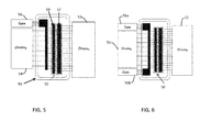
- the assembly of the package is shown in Figures 5 and 6 , and the assembly is designed to ensure uniform loading of the different cells in the RF power bar and RF losses will be reduced.
- Figure 5 shows a first assembly
- the RF power transistor 50 has a gate bar and a drain bar.
- the drain bar has a first set of connections to a first drain pad 52 on one side of the power amplifier transistor and a second set of connections to a second drain pad 54 on the opposite side.
- a single gate pad 56 connects to the gate bar.
- the bottom of the transistor structure is the source and is attached to the flange of the package.
- the source is shown as the region 55.
- the drain bar of the transistor is shown a 57 and the gate bar is shown as 59.
- Figure 6 shows a second assembly, which differs from Figure 5 only in that there is a double gate feed with two gate pads 56a,56b.
- the general structure is the same, with an input network 70 connecting the Doherty amplifier input to the input of the main amplifier 10 and to the input of the at least one peaking amplifier 12, and an output network 72 connecting an output of the main amplifier and an output of the at least one peaking amplifier to the Doherty amplifier output,
- the impedance inverter 72 Only one of the drain outputs of the peaking device (node 3) is used with the output of the main device (node 2) to form the impedance inverter 72.
- Any kind of impedance inverter can be formed by choosing the proper characteristics of the network TN 1n .
- the network TN 1n is designed such that the impedance inverter formed by the network device and the package parasitics of the main and peaking device (Lb1, Lb2, Cpkg) has a characteristic impedance equal to the real optimum loading conditions of the main power amplifier device.
- the design of the network TN 1n takes account of the parasitics at the first drain output.
- This structure has no impedance transformation before power combining.
- the characteristic impedance of the quarter wave transmission line formed by TN1n , Lb, Cpkg and Cdev should be also equal to Ropt so the transmission line does not perform any impedance transformation.
- the power combining of the main and peaking devices 10,12 really occurs at the internal device node (node 4).
- the second output of the peaking device (node 5) is used to connect to the RF load through an impedance transformation network TN 2n .
- the nodes 2,3 and 5 define the package terminals of the device.
- the capacitance Cpkg is the drain lead capacitance at each package terminal and Lb1, Lb2 and Lb3 are the bondwire inductances.
- the characteristics of the network TN 2n can be chosen in such a way that it provides the wideband impedance transformation over the desired bandwidth.
- the design of the network TN 2n takes account of the parasitics at the second drain output, and the design can be independent of the design of the impedance inverter 72.
- TN1n is a transmission line with a certain impedance and electrical length such that it forms a quarter wave transmission line along with the parasitic of the drains of the main and peaking devices.
- TN2n can be any wideband impedance matching circuit.
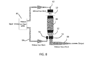
- Figure 8 shows one possible layout of a wideband broadcast power amplifier using the peaking amplifier of the invention.
- the input is provided to a wideband input signal splitter 80.
- Wideband input matching transmission lines 82, 84 connect to the main amplifier 10 and peaking amplifier 12.
- the transmission lines 82,84 provide the relative phase shifting of the input signal before amplification.
- the main amplifier and peaking amplifier have drain pads facing each other, in particular, the first drain pad 52 of the peaking amplifier.
- the impedance inverter is formed as a transmission line 86 between these drain pads, and this defines the impedance TN 1n of Figure 7 .
- the second drain pad 54 of the peaking amplifier 12 connects to the output load through a wideband output matching impedance 88, which defines the impedance TN 2n of Figure 7 .
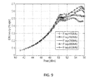
- Figure 9 shows a simulation of a broadcast Doherty power amplifier using the arrangement of Figure 8 , from 450Mhz to 850Mhz.
- the invention enables the wideband impedance inverters as disclosed in US 2012/0126890 to be used.
- Figures 10a and 10b show examples of the impedance inverter.
- it comprises the basic impedance inverter 100 and another electromagnetically coupled transmission line 102 which also connects to the an output node.
- the power combiner stage thus has two coupled transmission lines, each having a quarter wavelength based on the centre frequency of the amplifier.
- Coupled is meant that they share a common electric and magnetic field.
- the coupled lines 100,102 may be characterised by their even and odd mode impedances or alternatively by their geometrical dimensions.
- the transmission lines 100,102 may for example be implemented as symmetric strip lines or asymmetric micro strip lines.
- Figure 10a shows an optional third transmission line 104 with a length of at least a quarter wavelength connected between the second transmission line 102 of the coupled pair and the output node, which is thus also connected to the output of the main amplifier stage 12.
- one end of the transmission line 102 is open circuit.
- the third transmission line 104 may also be implemented be as symmetric strip lines or asymmetric micro strip lines.
- the third transmission line may is absent, and replaced by a short circuit, and the open end of the second transmission line 102 is connected to ground.
- the impedances of the transmission lines may be chosen such that the even and odd mode impedances of the coupled lines are 80 ⁇ (Zoe, or even mode impedance) and 44 ⁇ (Zoo, or odd mode impedance), and the impedance of the transmission line 75 ⁇ , and the electrical length of each of the lines selected to be one quarter wavelength. Other impedance values may alternatively be selected.
- the invention also enables the dual band inverters presented in the paper " A small dual-frequency transformer in two sections", C Monzon, IEEE Trans. on Microwave Theory and Tech. vol 51, April 2003, pp 1157-1161 to be used.
- the idea can be applied to the high-power amplifiers for cellular base-stations as well as multi-band broadcast amplifiers.
- the structure of the invention facilitates bandwidth improvement by allowing power combining in the Doherty amplifier at the peaking transistor die, thus eliminating the need for any additional network.
- the Doherty combiner is formed with the parasitics of the package.
Landscapes
- Engineering & Computer Science (AREA)
- Power Engineering (AREA)
- Amplifiers (AREA)
Abstract
Description
- The invention relates to an electronic device comprising a Doherty Amplifier ("DA") with an amplifier input and an amplifier output, wherein the amplifier has a main stage, and at least one peaking stage.
- An amplifier of this type has an input network connecting the amplifier input to an input of the main stage and to an input of the peaking stage. An output network connects an output of the main stage and an output of the peaking stage to the amplifier output.
- A classical DA has two amplifying stages arranged in parallel and of the same power capability. The first one of the stages (main stage) operates in a class - AB amplifier mode and the second one (peaking stage) operates in a class-C amplifier mode.
- These stages are separated at their inputs and at their outputs by 90 degree phase shifting networks. The output phase shifting network has a specific characteristic impedance Zo which must be equal to the optimal load impedance RLm of the main stage. The input signal is split so as to drive the two amplifiers, and a summing network, known as an "impedance inverter" or a "Doherty combiner", is operative to:
- a) combine the two output signals,
- b) correct for phase differences between the two output signals, and
- c) provide an inverted impedance at the output of the DA with respect to the impedance as seen from the output of the main stage.
- The Doherty amplifier addresses the problem that signals with significant amplitude modulation result in low average efficiency for the traditional power amplifier.
- The classical Doherty amplifier is a so-called 2-way amplifier with a main stage and a single peaking stage. A multi-way (or N-way) Doherty amplifier has a main stage and a plurality of peaking stages operating in parallel. An advantage of a multi-way Doherty system is that it extends the back-off level beyond the symmetrical two way design without exhibiting significant drop in efficiency between the efficiency peaking points. As a result, an improvement of efficiency is possible at 12dB power back-off, not at 6dB back-off as for a symmetrical 2-way Doherty amplifier. The 12dB power back-off is currently demanded by new communication systems such as 3 G-LTE (third generation long-term evolution) and WiMAX (Worldwide Interoperability for Microwave Access).
- Typically, the main stage and the peaking stages are implemented using a respective power transistor as each of the respective stages.
- An equivalent circuit of the classical two-way Doherty architecture is shown in
Figure 1 . Two Power Amplifiers ("PAs"); amain amplifier 10 and a peakingamplifier 12 of equal power capacity, are driven by the input, with a λ/4 line at the input of the peaking amplifier 12 (not shown in the equivalent circuit). This functions as an impedance aligner. Animpedance inverter 16 combines the output. -
Figure 2 shows the instantaneous efficiency of the two-way Doherty power amplifier ofFigure 1 (plot 20) as well as the efficiency of an ideal class-B amplifier (plot 22). The input λ/4 line dynamically modulates the load impedances of both main and peaking amplifiers as the input power level changes, improving the efficiency at back-off as shown inFigure 2 . - Doherty amplification is thus a well known technique for improving the power efficiency of RF transmitters when dealing with modulated signals that have high peak-to-average ratios e.g. MC-GSM, WCDMA and OFDM. In this context, power efficiency is defined as the ratio of average output power of the power amplifier to the DC input power. In these applications, the Doherty power amplifiers are applied to broadcast applications at sub-gigahertz frequencies for improving the average efficiency. The concept is very successful in improving the average efficiency of the transmitters and can provide average efficiencies more than 50% for the modern WCDMA and MC-GSM signals and is being widely used in the current cellular as well as broadcast base-station transmitters.
- However, the requirements of microwave transmitters are now shifting towards wider RF bandwidths along with high average efficiencies. For example, transmitted signals for the next generations of base-station transmitters have bandwidths in excess of 100 MHz and if the pre-distortion overhead on the bandwidth is included, the power amplifier for those signals need to handle signal bandwidths of more than 400MHz.
- Additionally, there is also a growing demand for multi-band high average efficiency power amplifiers. For example, in broadcast applications a multi-band amplifier is required which can operate over a very wide bandwidth e.g. from 460MHz to 860MHz with an average efficiency drop of no more than 10 percentage points from its maximum value, and peak power drop of not more than 0.5dB in the band.
- The current Doherty power amplifier implementations can provide high average efficiency, but their bandwidth performance is inadequate for the future needs of the base-stations and broadcast transmitters. For example the current high-power implementations cannot provide fractional efficiency bandwidths of more than 10% (assuming 10% drop of efficiency within the band). Note that this bandwidth is calculated at the average power levels, as the Doherty PA shows worst bandwidth limitations at these power levels.
- Fractional bandwidth is defined as

Δω =ω2-ω1 (ω1 and ω2 are frequencies where the relative efficiency drops by 10%. - It has been shown that the Doherty PA concept, in its most basic form, can provide the relative efficiency bandwidth of 28%.
- This bandwidth can be improved by using more complicated wideband impedance inverters. This approach is disclosed in
US 2012/0126890 . The impedance inverter comprises thebasic impedance inverter 16 shown inFigure 1 and another electromagnetically coupled transmission line which also connects to the load. When using this wideband impedance inverter with the basic schematic ofFigure 1 , the bandwidth of the Doherty PA can be further improved. - However, the bandwidth of the impedance inverter is not the only limiting factor for the bandwidth of the high-power Doherty PAs. It was also shown in
US 2012/0126890 that if the amplifier is made with bare dies and the output capacitances can be absorbed in the impedance inverter, the bandwidth of the Doherty PA can approach the theoretical limit of what can be achieved by using the quarter wave transmission line. However the technique cannot be directly applied to an amplifier implemented using packaged high-power PA devices, in particular as a result of the parasitic impedances associated with the package leads. - This invention aims to broaden the bandwidth of the high power Doherty PA by the use of a specialized layout and packaging.
- According to the invention, there is provided an amplifier as claimed in
claim 1. - The invention provides a Doherty amplifier for driving a load comprising:
- a main amplifier;
- at least one peaking amplifier;
- an input network connecting the Doherty amplifier input to the input of the main amplifier and to the input of the at least one peaking amplifier; and
- an output network connecting an output of the main amplifier and an output of the at least one peaking amplifier,
- wherein the at least one peaking amplifier comprises first and second drain connections, wherein the first drain connection is connected to the output network, and the second drain connection is connected to the load.
- By providing a peaking amplifier with two drain outputs, the bandwidth of the Doherty Power Amplifier can be increased. One drain output is used with the main amplifier to form the wideband impedance inverter required for the Doherty PA operation and the other drain output is used to connect to the RF load.
- A transmission network can be provided between the second drain output and the load, in particular a wideband impedance transformation network. The choice of proper matching network at the second drain output can provide a relative bandwidth in excess of 45%.
- The output network can comprise a first phase shifting element between the output of the main amplifier and the Doherty amplifier output, and a second phase shifting element electromagnetically coupled to the first phase shifting element, and in series to the Doherty amplifier output. This output network (impedance inverter) gives improved operation of the wavelength band or enables an increased wavelength band.
- A third phase shifting element can be in series between the second phase shifting element and the Doherty amplifier output.
- The invention also provides an amplification method using a Doherty amplifier having a main amplifier and at least one peaking amplifier having first and second drain connections, the method comprising:
- connecting the Doherty amplifier input to the input of the main amplifier and to the input of the at least one peaking amplifier through an input network;
- connecting an output of the main amplifier and an output of the at least one peaking amplifier using an output network; and
- connecting the first drain connection of the peaking amplifier to the output network and connecting the second drain connection of the at least one peaking amplifier to a load.
- Examples of the invention will now be described in detail with reference to the accompanying drawings, in which:
-
Figure 1 shows an equivalent circuit for the basic known two way Doherty Power Amplifier; -
Figure 2 compares the efficiency of the Doherty PA ofFigure 1 with an ideal Class-B amplifier; -
Figure 3 shows a known component layout for a packaged two way Doherty power amplifier circuit; -
Figure 4 shows a peaking amplifier stage in accordance with the invention; -
Figure 5 shows a first physical layout for the peaking amplifier; -
Figure 6 shows a second physical layout for the peaking amplifier; -
Figure 7 shows a component layout for a packaged two way Doherty power amplifier circuit of the invention; -
Figure 8 shows a physical layout for the whole Doherty amplifier; -
Figure 9 shows the efficiency as a function of output power at different frequencies; and -
Figures 10a and 10b show different possible impedance inverters that can be used in the circuit. - The invention provides a Doherty amplifier which has at least one peaking amplifier which has first and second drain connections, wherein the first drain connection is connected to the output network, and the second drain connection is connection to the load. By providing two drain connections, separate package leads to the peaking amplifier can be taken into account when designing the impedance inverter and an output impedance. In this way, the circuit operation can be optimised both for the impedance inversion function and for driving the output load.
- Before explaining the details of this invention a description will first be provided concerning the bandwidth limiting factors for a high-power Doherty PA constructed using packaged PA devices.
- For this purpose, a schematic diagram of a conventional high-power Doherty PA is shown in the
Figure 3 . - Lb1 and Lb2 represent the parasitic bond-wire inductances resulting from the connection of the RF power transistor to the package lead, Cpkg represents the capacitance of the packaged lead and Cd represents the output capacitance of the power amplifier ("PA") devices.
- Six nodes are labelled in
Figure 3 as 1 to 6. - The inductors Lb1, Lb2, the package capacitors Cpkg and the capacitors Cd are inside the package. Outside the package are transmission lines TN2 and TN2 which are connected between the main and peaking devices to form the remaining part of the impedance inverter.
- The device parasitic capacitance Cd along with the package parasitic Lb1 and Cpkg cause undesired rotation of the impedances from the
node 2 to the internal current source (node 1), thereby disturbing the Doherty PA operation. Therefore in order to apply correct load modulation at the internal current source, a passive transformation network (TN1) is inserted between the impedance inverter and the package lead which makes the total transformation from thenode 1 to thenode 3 equal to zero or 180° at the operating frequency. - Moreover, a similar network (TN2) is added at the peaking device, in order to present high impedance to the main device under power back-off conditions (when the peaking device is off). This approach works well at the designed frequency, but the frequency response of the networks TN1 and TN2 severely limits the bandwidth performance of the Doherty PA, and in practice the bandwidth of the Doherty PA is more limited by the bandwidth of the transformation networks TN1 and TN2 rather than the impedance inverter itself.
- Therefore, the use of a wideband impedance inverter as disclosed in
US 2012/0126890 in such conventionally designed Doherty PA circuits do not show optimum bandwidth improvements. Similarly, the dual band inverters presented in the paper "A small dual-frequency transformer in two sections", C Monzon, IEEE Trans. on Microwave Theory and Tech. vol 51, April 2003, pp 1157-1161 do not give rise to the desired bandwidth improvements. - This invention aims to eliminate the networks TN1 and TN2 by the use of specialized layout and packaging of the peaking device, including a circuit connection scheme, in order to improve the bandwidth of the Doherty PA constructed with this device.
- The invention provides a modified Doherty PA configuration which can directly benefit from the use of the improved wideband and multi-band impedance inverters disclosed in the references above, and provides a significantly improved bandwidth performance.
- The invention provides a peaking amplifier with two output leads as shown in
Figure 4 . - The power amplifier transistor is shown, with two drain connections Drain1 and Drain2. Each of these is associated with a bond wire with inductance and capacitance.
- Cd in
Figure 4 represents the output capacitance of the power amplifier device, Lb1 and Lb2 are the bond-wire inductances and Cpkg1 and Cpkg2 are the package parasitic capacitances. - The assembly of the package is shown in
Figures 5 and 6 , and the assembly is designed to ensure uniform loading of the different cells in the RF power bar and RF losses will be reduced. -
Figure 5 shows a first assembly. - The
RF power transistor 50 has a gate bar and a drain bar. The drain bar has a first set of connections to afirst drain pad 52 on one side of the power amplifier transistor and a second set of connections to asecond drain pad 54 on the opposite side. Asingle gate pad 56 connects to the gate bar. - The bottom of the transistor structure is the source and is attached to the flange of the package. The source is shown as the
region 55. The drain bar of the transistor is shown a 57 and the gate bar is shown as 59. -
Figure 6 shows a second assembly, which differs fromFigure 5 only in that there is a double gate feed with twogate pads - The complete circuit diagram of the modified Doherty PA using the peaking device of the invention is shown in
Figure 7 . This shows five nodes numbered 1 to 5. - The general structure is the same, with an
input network 70 connecting the Doherty amplifier input to the input of themain amplifier 10 and to the input of the at least one peakingamplifier 12, and an output network 72 connecting an output of the main amplifier and an output of the at least one peaking amplifier to the Doherty amplifier output, - Only one of the drain outputs of the peaking device (node 3) is used with the output of the main device (node 2) to form the impedance inverter 72. This includes a network TN1n. Any kind of impedance inverter (wideband impedance inverter or multi-band impedance inverter) can be formed by choosing the proper characteristics of the network TN1n.
- The network TN1n is designed such that the impedance inverter formed by the network device and the package parasitics of the main and peaking device (Lb1, Lb2, Cpkg) has a characteristic impedance equal to the real optimum loading conditions of the main power amplifier device. Thus, the design of the network TN1n takes account of the parasitics at the first drain output.
- This structure has no impedance transformation before power combining. For example if the optimum load of the PA devices is Ropt, the characteristic impedance of the quarter wave transmission line formed by TN1n , Lb, Cpkg and Cdev should be also equal to Ropt so the transmission line does not perform any impedance transformation.
- The power combining of the main and peaking
devices - The second output of the peaking device (node 5) is used to connect to the RF load through an impedance transformation network TN2n.
- The
nodes - The characteristics of the network TN2n can be chosen in such a way that it provides the wideband impedance transformation over the desired bandwidth.
- Thus, the design of the network TN2n takes account of the parasitics at the second drain output, and the design can be independent of the design of the impedance inverter 72.
- TN1n is a transmission line with a certain impedance and electrical length such that it forms a quarter wave transmission line along with the parasitic of the drains of the main and peaking devices. TN2n can be any wideband impedance matching circuit.
-
Figure 8 shows one possible layout of a wideband broadcast power amplifier using the peaking amplifier of the invention. - The input is provided to a wideband
input signal splitter 80. Wideband input matchingtransmission lines main amplifier 10 and peakingamplifier 12. Thetransmission lines - The main amplifier and peaking amplifier have drain pads facing each other, in particular, the
first drain pad 52 of the peaking amplifier. The impedance inverter is formed as atransmission line 86 between these drain pads, and this defines the impedance TN1n ofFigure 7 . Thesecond drain pad 54 of the peakingamplifier 12 connects to the output load through a widebandoutput matching impedance 88, which defines the impedance TN2n ofFigure 7 . -
Figure 9 shows a simulation of a broadcast Doherty power amplifier using the arrangement ofFigure 8 , from 450Mhz to 850Mhz. - As mentioned above, the invention enables the wideband impedance inverters as disclosed in
US 2012/0126890 to be used. -
Figures 10a and 10b show examples of the impedance inverter. In each case, it comprises thebasic impedance inverter 100 and another electromagnetically coupledtransmission line 102 which also connects to the an output node. The power combiner stage thus has two coupled transmission lines, each having a quarter wavelength based on the centre frequency of the amplifier. - By "coupled" is meant that they share a common electric and magnetic field.
- The coupled lines 100,102 may be characterised by their even and odd mode impedances or alternatively by their geometrical dimensions. The transmission lines 100,102 may for example be implemented as symmetric strip lines or asymmetric micro strip lines.
-
Figure 10a shows an optionalthird transmission line 104 with a length of at least a quarter wavelength connected between thesecond transmission line 102 of the coupled pair and the output node, which is thus also connected to the output of themain amplifier stage 12. InFigure 10a , one end of thetransmission line 102 is open circuit. - The
third transmission line 104 may also be implemented be as symmetric strip lines or asymmetric micro strip lines. - In an alternative embodiment shown in
Figure 10b , the third transmission line may is absent, and replaced by a short circuit, and the open end of thesecond transmission line 102 is connected to ground. - The impedances of the transmission lines may be chosen such that the even and odd mode impedances of the coupled lines are 80Ω (Zoe, or even mode impedance) and 44 Ω (Zoo, or odd mode impedance), and the impedance of the transmission line 75Ω, and the electrical length of each of the lines selected to be one quarter wavelength. Other impedance values may alternatively be selected.
- When using this wideband impedance inverter with the basic schematic of
Figure 1 , the bandwidth of the Doherty PA can be further improved. - The invention also enables the dual band inverters presented in the paper "A small dual-frequency transformer in two sections", C Monzon, IEEE Trans. on Microwave Theory and Tech. vol 51, April 2003, pp 1157-1161 to be used.
- The idea can be applied to the high-power amplifiers for cellular base-stations as well as multi-band broadcast amplifiers.
- The structure of the invention facilitates bandwidth improvement by allowing power combining in the Doherty amplifier at the peaking transistor die, thus eliminating the need for any additional network. The Doherty combiner is formed with the parasitics of the package.
- Other variations to the disclosed embodiments can be understood and effected by those skilled in the art in practicing the claimed invention, from a study of the drawings, the disclosure, and the appended claims. In the claims, the word "comprising" does not exclude other elements or steps, and the indefinite article "a" or "an" does not exclude a plurality. The mere fact that certain measures are recited in mutually different dependent claims does not indicate that a combination of these measured cannot be used to advantage. Any reference signs in the claims should not be construed as limiting the scope.
Claims (9)
- A Doherty amplifier for driving a load comprising:a main amplifier (10);at least one peaking amplifier (12);an input network(70) connecting the Doherty amplifier input to the input of the main amplifier (10) and to the input of the at least one peaking amplifier (12); andan output network (72) connecting an output of the main amplifier (10) and an output of the at least one peaking amplifier (12)wherein the at least one peaking amplifier (12) comprises first and second drain connections, wherein the first drain connection is connected to the output network (72), and the second drain connection is connected to the load.
- An amplifier as claimed in claim 1, wherein the output network (TN1n) comprises a transmission line with an impedance and electrical length such that it forms a quarter wave transmission line along with the parasitic capacitances and inductances (Lb1, Lb2, Cpkg) of the drain connection of the main amplifier and the first drain connection of the peaking amplifier.
- An amplifier as claimed in claim 1 or 2, comprising a transmission network (TN2n) between the second drain connection and the load.
- An amplifier as claimed in claim 3, wherein the transmission network is a wideband impedance matching circuit.
- An amplifier as claimed in any preceding claim, wherein the output network (72) comprises a first phase shifting element (100) between the output of the main amplifier (10) and an output node, and a second phase shifting element (102) electromagnetically coupled to the first phase shifting element, and in series to the output.
- An amplifier as claimed in claim 5, further comprising a third phase shifting element (104) in series between the second phase shifting element and the output node.
- A radio frequency transmitter comprising a Doherty amplifier as claimed in any preceding claim.
- An integrated circuit comprising a Doherty amplifier as claimed in any one of claims 1 to 6.
- An amplification method using a Doherty amplifier having a main amplifier and at least one peaking amplifier having first and second drain connections, the method comprising:connecting the Doherty amplifier input to the input of the main amplifier and to the input of the at least one peaking amplifier through an input network (70);connecting an output of the main amplifier (10) and an output of the at least one peaking amplifier (12) using an output network (72); andconnecting the first drain connection of the peaking amplifier to the output network (72) and connecting the second drain connection of the at least one peaking amplifier to a load.
Priority Applications (2)
| Application Number | Priority Date | Filing Date | Title |
|---|---|---|---|
| EP13173865.0A EP2819304B1 (en) | 2013-06-26 | 2013-06-26 | Doherty amplifier |
| US14/301,423 US9496837B2 (en) | 2013-06-26 | 2014-06-11 | Doherty amplifier |
Applications Claiming Priority (1)
| Application Number | Priority Date | Filing Date | Title |
|---|---|---|---|
| EP13173865.0A EP2819304B1 (en) | 2013-06-26 | 2013-06-26 | Doherty amplifier |
Publications (2)
| Publication Number | Publication Date |
|---|---|
| EP2819304A1 true EP2819304A1 (en) | 2014-12-31 |
| EP2819304B1 EP2819304B1 (en) | 2018-12-19 |
Family
ID=48670459
Family Applications (1)
| Application Number | Title | Priority Date | Filing Date |
|---|---|---|---|
| EP13173865.0A Active EP2819304B1 (en) | 2013-06-26 | 2013-06-26 | Doherty amplifier |
Country Status (2)
| Country | Link |
|---|---|
| US (1) | US9496837B2 (en) |
| EP (1) | EP2819304B1 (en) |
Cited By (3)
| Publication number | Priority date | Publication date | Assignee | Title |
|---|---|---|---|---|
| CN105874706A (en) * | 2014-01-06 | 2016-08-17 | 华为技术有限公司 | Doherty power amplifier, communication device and system |
| CN109818581A (en) * | 2017-12-04 | 2019-05-28 | 恩智浦美国有限公司 | The multichannel pmultiple amplifier of series component with the phase inverter between amplifier out |
| WO2023070474A1 (en) * | 2021-10-28 | 2023-05-04 | 华为技术有限公司 | Multi-band power amplification circuit, radio frequency transceiver, and base station |
Families Citing this family (17)
| Publication number | Priority date | Publication date | Assignee | Title |
|---|---|---|---|---|
| JP6812091B2 (en) * | 2014-05-29 | 2021-01-13 | 日東電工株式会社 | Soft magnetic resin composition and soft magnetic film |
| EP3264595B1 (en) * | 2016-06-30 | 2020-02-26 | Nxp B.V. | Doherty amplifiers |
| US11233483B2 (en) | 2017-02-02 | 2022-01-25 | Macom Technology Solutions Holdings, Inc. | 90-degree lumped and distributed Doherty impedance inverter |
| WO2018197918A1 (en) | 2017-04-24 | 2018-11-01 | Macom Technology Solutions Holdings, Inc. | Improved efficiency, symmetrical doherty power amplifier |
| US11159125B2 (en) | 2017-04-24 | 2021-10-26 | Macom Technology Solutions Holdings, Inc. | Inverted Doherty power amplifier with large RF fractional and instantaneous bandwidths |
| WO2018197919A1 (en) | 2017-04-24 | 2018-11-01 | Macom Technology Solutions Holdings, Inc. | Inverted doherty power amplifier with large rf and instantaneous bandwidths |
| US10033335B1 (en) | 2017-05-08 | 2018-07-24 | City University Of Hong Kong | Doherty power amplifier |
| FR3070100A1 (en) | 2017-08-14 | 2019-02-15 | Macom Technology Solutions Holdings, Inc. | POWERFUL AMPLIFIER ARCHITECTURE WITHOUT MODULATION, BROADBAND AND HIGH EFFICIENCY |
| US11283410B2 (en) * | 2017-10-02 | 2022-03-22 | Macom Technology Solutions Holdings, Inc. | No-load-modulation, high-efficiency power amplifier |
| US11705869B2 (en) | 2018-10-05 | 2023-07-18 | Macom Technology Solutions Holdings, Inc. | Low-load-modulation power amplifier |
| US11201591B2 (en) * | 2019-03-20 | 2021-12-14 | Cree, Inc. | Asymmetric Doherty amplifier circuit with shunt reactances |
| CN114430884B (en) * | 2019-10-02 | 2024-11-12 | 三菱电机株式会社 | Doherty Amplifier |
| US11888448B2 (en) | 2019-12-30 | 2024-01-30 | Macom Technology Solutions Holdings, Inc. | Low-load-modulation broadband amplifier |
| CN111510077A (en) * | 2020-04-24 | 2020-08-07 | 苏州远创达科技有限公司 | A Wideband Doherty Amplifier |
| US12028022B2 (en) | 2020-12-10 | 2024-07-02 | Macom Technology Solutions Holdings, Inc. | Hybrid power amplifier with GaN-on-Si and GaN-on-SiC circuits |
| US12603622B2 (en) | 2021-10-29 | 2026-04-14 | Analog Devices International Unlimited Company | Apparatus and methods for radio frequency amplifiers |
| CN119276230A (en) * | 2023-07-05 | 2025-01-07 | 苏州远创达科技有限公司 | A cascaded Doherty power amplifier |
Citations (4)
| Publication number | Priority date | Publication date | Assignee | Title |
|---|---|---|---|---|
| US20090045878A1 (en) * | 2003-09-17 | 2009-02-19 | Nec Corporation | Amplifier |
| US20100200979A1 (en) * | 2009-02-09 | 2010-08-12 | Infineon Technologies North America Corp. | Power Transistor Package with Integrated Bus Bar |
| US20120126890A1 (en) | 2010-04-23 | 2012-05-24 | Nxp B.V. | Power amplifier |
| EP2463905A1 (en) * | 2010-12-10 | 2012-06-13 | Nxp B.V. | Packaged RF transistor with special supply voltage leads |
Family Cites Families (6)
| Publication number | Priority date | Publication date | Assignee | Title |
|---|---|---|---|---|
| WO2008062371A2 (en) | 2006-11-23 | 2008-05-29 | Nxp B.V. | Integrated doherty type amplifier arrangement with high power efficiency |
| US8228123B2 (en) * | 2007-08-29 | 2012-07-24 | Nxp B.V. | Integrated Doherty amplifier |
| EP2339745A1 (en) * | 2009-12-15 | 2011-06-29 | Nxp B.V. | Doherty amplifier |
| US8314654B2 (en) * | 2010-05-17 | 2012-11-20 | Alcatel Lucent | Multi-band high-efficiency Doherty amplifier |
| EP2458730B8 (en) * | 2010-11-29 | 2015-08-05 | Nxp B.V. | Radiofrequency amplifier |
| US8717102B2 (en) * | 2011-09-27 | 2014-05-06 | Infineon Technologies Ag | RF device with compensatory resonator matching topology |
-
2013
- 2013-06-26 EP EP13173865.0A patent/EP2819304B1/en active Active
-
2014
- 2014-06-11 US US14/301,423 patent/US9496837B2/en active Active
Patent Citations (4)
| Publication number | Priority date | Publication date | Assignee | Title |
|---|---|---|---|---|
| US20090045878A1 (en) * | 2003-09-17 | 2009-02-19 | Nec Corporation | Amplifier |
| US20100200979A1 (en) * | 2009-02-09 | 2010-08-12 | Infineon Technologies North America Corp. | Power Transistor Package with Integrated Bus Bar |
| US20120126890A1 (en) | 2010-04-23 | 2012-05-24 | Nxp B.V. | Power amplifier |
| EP2463905A1 (en) * | 2010-12-10 | 2012-06-13 | Nxp B.V. | Packaged RF transistor with special supply voltage leads |
Non-Patent Citations (1)
| Title |
|---|
| C MONZON: "A small dual-frequency transformer in two sections", IEEE TRANS. ON MICROWAVE THEORY AND TECH, vol. 51, April 2003 (2003-04-01), pages 1157 - 1161, XP001145356, DOI: doi:10.1109/TMTT.2003.809675 |
Cited By (6)
| Publication number | Priority date | Publication date | Assignee | Title |
|---|---|---|---|---|
| CN105874706A (en) * | 2014-01-06 | 2016-08-17 | 华为技术有限公司 | Doherty power amplifier, communication device and system |
| JP2017501662A (en) * | 2014-01-06 | 2017-01-12 | ホアウェイ・テクノロジーズ・カンパニー・リミテッド | Doherty power amplifier, communication device, and system |
| US9876474B2 (en) | 2014-01-06 | 2018-01-23 | Huawei Technologies Co., Ltd | Doherty power amplifier, communications device, and system |
| CN105874706B (en) * | 2014-01-06 | 2020-03-20 | 华为技术有限公司 | Doherty power amplifier, communication device and system |
| CN109818581A (en) * | 2017-12-04 | 2019-05-28 | 恩智浦美国有限公司 | The multichannel pmultiple amplifier of series component with the phase inverter between amplifier out |
| WO2023070474A1 (en) * | 2021-10-28 | 2023-05-04 | 华为技术有限公司 | Multi-band power amplification circuit, radio frequency transceiver, and base station |
Also Published As
| Publication number | Publication date |
|---|---|
| US20150002230A1 (en) | 2015-01-01 |
| US9496837B2 (en) | 2016-11-15 |
| EP2819304B1 (en) | 2018-12-19 |
Similar Documents
| Publication | Publication Date | Title |
|---|---|---|
| EP2819304B1 (en) | Doherty amplifier | |
| EP2806557B1 (en) | Doherty amplifier | |
| CN102480272B (en) | Radiofrequency amplifier | |
| US10250192B2 (en) | Class-E outphasing power amplifier with efficiency and output power enhancement circuits and method | |
| US9048020B2 (en) | Bond wire transformer | |
| US9531328B2 (en) | Amplifiers with a short phase path, packaged RF devices for use therein, and methods of manufacture thereof | |
| US8174322B2 (en) | Power control of reconfigurable outphasing chireix amplifiers and methods | |
| US8203386B2 (en) | Reconfigurable outphasing Chireix amplifiers and methods | |
| EP1763921B1 (en) | Integrated doherty type amplifier arrangement with high power efficiency | |
| CN104601117B (en) | Doherty amplifier structure | |
| US20100001802A1 (en) | Integrated doherty type amplifier arrangement with high power efficiency | |
| EP2698918A1 (en) | Amplifier circuit | |
| US9071198B2 (en) | Amplifier circuit | |
| US20160308495A1 (en) | Wideband doherty amplifier circuit with integrated transformer line balun | |
| CN106664062B (en) | Integrated 3-way Doherty amplifier | |
| Lee et al. | A CMOS outphasing power amplifier with integrated single-ended Chireix combiner | |
| EP2958232A1 (en) | Doherty amplifier | |
| Hayakawa et al. | A total bandwidth expanded dual-band GaN Doherty PA toward the LTE-A carrier aggregation application | |
| Houssein et al. | A 70W dual-band high efficiency MMIC Doherty PA linearized over 200MHz iBW for 2.3-2.7 GHz macro base station driver applications |
Legal Events
| Date | Code | Title | Description |
|---|---|---|---|
| PUAI | Public reference made under article 153(3) epc to a published international application that has entered the european phase |
Free format text: ORIGINAL CODE: 0009012 |
|
| 17P | Request for examination filed |
Effective date: 20140326 |
|
| AK | Designated contracting states |
Kind code of ref document: A1 Designated state(s): AL AT BE BG CH CY CZ DE DK EE ES FI FR GB GR HR HU IE IS IT LI LT LU LV MC MK MT NL NO PL PT RO RS SE SI SK SM TR |
|
| AX | Request for extension of the european patent |
Extension state: BA ME |
|
| RBV | Designated contracting states (corrected) |
Designated state(s): AL AT BE BG CH CY CZ DE DK EE ES FI FR GB GR HR HU IE IS IT LI LT LU LV MC MK MT NL NO PL PT RO RS SE SI SK SM TR |
|
| 17Q | First examination report despatched |
Effective date: 20150630 |
|
| RAP1 | Party data changed (applicant data changed or rights of an application transferred) |
Owner name: SAMBA HOLDCO NETHERLANDS B.V. |
|
| RAP1 | Party data changed (applicant data changed or rights of an application transferred) |
Owner name: AMPLEON NETHERLANDS B.V. |
|
| STAA | Information on the status of an ep patent application or granted ep patent |
Free format text: STATUS: EXAMINATION IS IN PROGRESS |
|
| GRAP | Despatch of communication of intention to grant a patent |
Free format text: ORIGINAL CODE: EPIDOSNIGR1 |
|
| STAA | Information on the status of an ep patent application or granted ep patent |
Free format text: STATUS: GRANT OF PATENT IS INTENDED |
|
| INTG | Intention to grant announced |
Effective date: 20180629 |
|
| GRAS | Grant fee paid |
Free format text: ORIGINAL CODE: EPIDOSNIGR3 |
|
| GRAA | (expected) grant |
Free format text: ORIGINAL CODE: 0009210 |
|
| STAA | Information on the status of an ep patent application or granted ep patent |
Free format text: STATUS: THE PATENT HAS BEEN GRANTED |
|
| AK | Designated contracting states |
Kind code of ref document: B1 Designated state(s): AL AT BE BG CH CY CZ DE DK EE ES FI FR GB GR HR HU IE IS IT LI LT LU LV MC MK MT NL NO PL PT RO RS SE SI SK SM TR |
|
| REG | Reference to a national code |
Ref country code: GB Ref legal event code: FG4D |
|
| REG | Reference to a national code |
Ref country code: CH Ref legal event code: EP |
|
| REG | Reference to a national code |
Ref country code: IE Ref legal event code: FG4D |
|
| REG | Reference to a national code |
Ref country code: DE Ref legal event code: R096 Ref document number: 602013048348 Country of ref document: DE |
|
| REG | Reference to a national code |
Ref country code: AT Ref legal event code: REF Ref document number: 1079770 Country of ref document: AT Kind code of ref document: T Effective date: 20190115 |
|
| REG | Reference to a national code |
Ref country code: NL Ref legal event code: FP |
|
| PG25 | Lapsed in a contracting state [announced via postgrant information from national office to epo] |
Ref country code: LV Free format text: LAPSE BECAUSE OF FAILURE TO SUBMIT A TRANSLATION OF THE DESCRIPTION OR TO PAY THE FEE WITHIN THE PRESCRIBED TIME-LIMIT Effective date: 20181219 Ref country code: FI Free format text: LAPSE BECAUSE OF FAILURE TO SUBMIT A TRANSLATION OF THE DESCRIPTION OR TO PAY THE FEE WITHIN THE PRESCRIBED TIME-LIMIT Effective date: 20181219 Ref country code: BG Free format text: LAPSE BECAUSE OF FAILURE TO SUBMIT A TRANSLATION OF THE DESCRIPTION OR TO PAY THE FEE WITHIN THE PRESCRIBED TIME-LIMIT Effective date: 20190319 Ref country code: NO Free format text: LAPSE BECAUSE OF FAILURE TO SUBMIT A TRANSLATION OF THE DESCRIPTION OR TO PAY THE FEE WITHIN THE PRESCRIBED TIME-LIMIT Effective date: 20190319 Ref country code: HR Free format text: LAPSE BECAUSE OF FAILURE TO SUBMIT A TRANSLATION OF THE DESCRIPTION OR TO PAY THE FEE WITHIN THE PRESCRIBED TIME-LIMIT Effective date: 20181219 Ref country code: LT Free format text: LAPSE BECAUSE OF FAILURE TO SUBMIT A TRANSLATION OF THE DESCRIPTION OR TO PAY THE FEE WITHIN THE PRESCRIBED TIME-LIMIT Effective date: 20181219 |
|
| REG | Reference to a national code |
Ref country code: LT Ref legal event code: MG4D |
|
| REG | Reference to a national code |
Ref country code: AT Ref legal event code: MK05 Ref document number: 1079770 Country of ref document: AT Kind code of ref document: T Effective date: 20181219 |
|
| PG25 | Lapsed in a contracting state [announced via postgrant information from national office to epo] |
Ref country code: SE Free format text: LAPSE BECAUSE OF FAILURE TO SUBMIT A TRANSLATION OF THE DESCRIPTION OR TO PAY THE FEE WITHIN THE PRESCRIBED TIME-LIMIT Effective date: 20181219 Ref country code: GR Free format text: LAPSE BECAUSE OF FAILURE TO SUBMIT A TRANSLATION OF THE DESCRIPTION OR TO PAY THE FEE WITHIN THE PRESCRIBED TIME-LIMIT Effective date: 20190320 Ref country code: AL Free format text: LAPSE BECAUSE OF FAILURE TO SUBMIT A TRANSLATION OF THE DESCRIPTION OR TO PAY THE FEE WITHIN THE PRESCRIBED TIME-LIMIT Effective date: 20181219 Ref country code: RS Free format text: LAPSE BECAUSE OF FAILURE TO SUBMIT A TRANSLATION OF THE DESCRIPTION OR TO PAY THE FEE WITHIN THE PRESCRIBED TIME-LIMIT Effective date: 20181219 |
|
| PG25 | Lapsed in a contracting state [announced via postgrant information from national office to epo] |
Ref country code: PT Free format text: LAPSE BECAUSE OF FAILURE TO SUBMIT A TRANSLATION OF THE DESCRIPTION OR TO PAY THE FEE WITHIN THE PRESCRIBED TIME-LIMIT Effective date: 20190419 Ref country code: CZ Free format text: LAPSE BECAUSE OF FAILURE TO SUBMIT A TRANSLATION OF THE DESCRIPTION OR TO PAY THE FEE WITHIN THE PRESCRIBED TIME-LIMIT Effective date: 20181219 Ref country code: ES Free format text: LAPSE BECAUSE OF FAILURE TO SUBMIT A TRANSLATION OF THE DESCRIPTION OR TO PAY THE FEE WITHIN THE PRESCRIBED TIME-LIMIT Effective date: 20181219 Ref country code: PL Free format text: LAPSE BECAUSE OF FAILURE TO SUBMIT A TRANSLATION OF THE DESCRIPTION OR TO PAY THE FEE WITHIN THE PRESCRIBED TIME-LIMIT Effective date: 20181219 Ref country code: IT Free format text: LAPSE BECAUSE OF FAILURE TO SUBMIT A TRANSLATION OF THE DESCRIPTION OR TO PAY THE FEE WITHIN THE PRESCRIBED TIME-LIMIT Effective date: 20181219 |
|
| PG25 | Lapsed in a contracting state [announced via postgrant information from national office to epo] |
Ref country code: IS Free format text: LAPSE BECAUSE OF FAILURE TO SUBMIT A TRANSLATION OF THE DESCRIPTION OR TO PAY THE FEE WITHIN THE PRESCRIBED TIME-LIMIT Effective date: 20190419 Ref country code: SK Free format text: LAPSE BECAUSE OF FAILURE TO SUBMIT A TRANSLATION OF THE DESCRIPTION OR TO PAY THE FEE WITHIN THE PRESCRIBED TIME-LIMIT Effective date: 20181219 Ref country code: RO Free format text: LAPSE BECAUSE OF FAILURE TO SUBMIT A TRANSLATION OF THE DESCRIPTION OR TO PAY THE FEE WITHIN THE PRESCRIBED TIME-LIMIT Effective date: 20181219 Ref country code: SM Free format text: LAPSE BECAUSE OF FAILURE TO SUBMIT A TRANSLATION OF THE DESCRIPTION OR TO PAY THE FEE WITHIN THE PRESCRIBED TIME-LIMIT Effective date: 20181219 Ref country code: EE Free format text: LAPSE BECAUSE OF FAILURE TO SUBMIT A TRANSLATION OF THE DESCRIPTION OR TO PAY THE FEE WITHIN THE PRESCRIBED TIME-LIMIT Effective date: 20181219 |
|
| REG | Reference to a national code |
Ref country code: DE Ref legal event code: R097 Ref document number: 602013048348 Country of ref document: DE |
|
| PLBE | No opposition filed within time limit |
Free format text: ORIGINAL CODE: 0009261 |
|
| STAA | Information on the status of an ep patent application or granted ep patent |
Free format text: STATUS: NO OPPOSITION FILED WITHIN TIME LIMIT |
|
| PG25 | Lapsed in a contracting state [announced via postgrant information from national office to epo] |
Ref country code: DK Free format text: LAPSE BECAUSE OF FAILURE TO SUBMIT A TRANSLATION OF THE DESCRIPTION OR TO PAY THE FEE WITHIN THE PRESCRIBED TIME-LIMIT Effective date: 20181219 Ref country code: AT Free format text: LAPSE BECAUSE OF FAILURE TO SUBMIT A TRANSLATION OF THE DESCRIPTION OR TO PAY THE FEE WITHIN THE PRESCRIBED TIME-LIMIT Effective date: 20181219 |
|
| 26N | No opposition filed |
Effective date: 20190920 |
|
| PG25 | Lapsed in a contracting state [announced via postgrant information from national office to epo] |
Ref country code: MC Free format text: LAPSE BECAUSE OF FAILURE TO SUBMIT A TRANSLATION OF THE DESCRIPTION OR TO PAY THE FEE WITHIN THE PRESCRIBED TIME-LIMIT Effective date: 20181219 |
|
| REG | Reference to a national code |
Ref country code: CH Ref legal event code: PL |
|
| PG25 | Lapsed in a contracting state [announced via postgrant information from national office to epo] |
Ref country code: SI Free format text: LAPSE BECAUSE OF FAILURE TO SUBMIT A TRANSLATION OF THE DESCRIPTION OR TO PAY THE FEE WITHIN THE PRESCRIBED TIME-LIMIT Effective date: 20181219 |
|
| REG | Reference to a national code |
Ref country code: BE Ref legal event code: MM Effective date: 20190630 |
|
| PG25 | Lapsed in a contracting state [announced via postgrant information from national office to epo] |
Ref country code: TR Free format text: LAPSE BECAUSE OF FAILURE TO SUBMIT A TRANSLATION OF THE DESCRIPTION OR TO PAY THE FEE WITHIN THE PRESCRIBED TIME-LIMIT Effective date: 20181219 |
|
| PG25 | Lapsed in a contracting state [announced via postgrant information from national office to epo] |
Ref country code: LI Free format text: LAPSE BECAUSE OF NON-PAYMENT OF DUE FEES Effective date: 20190630 Ref country code: CH Free format text: LAPSE BECAUSE OF NON-PAYMENT OF DUE FEES Effective date: 20190630 Ref country code: LU Free format text: LAPSE BECAUSE OF NON-PAYMENT OF DUE FEES Effective date: 20190626 Ref country code: BE Free format text: LAPSE BECAUSE OF NON-PAYMENT OF DUE FEES Effective date: 20190630 |
|
| PG25 | Lapsed in a contracting state [announced via postgrant information from national office to epo] |
Ref country code: CY Free format text: LAPSE BECAUSE OF FAILURE TO SUBMIT A TRANSLATION OF THE DESCRIPTION OR TO PAY THE FEE WITHIN THE PRESCRIBED TIME-LIMIT Effective date: 20181219 |
|
| PG25 | Lapsed in a contracting state [announced via postgrant information from national office to epo] |
Ref country code: HU Free format text: LAPSE BECAUSE OF FAILURE TO SUBMIT A TRANSLATION OF THE DESCRIPTION OR TO PAY THE FEE WITHIN THE PRESCRIBED TIME-LIMIT; INVALID AB INITIO Effective date: 20130626 Ref country code: MT Free format text: LAPSE BECAUSE OF FAILURE TO SUBMIT A TRANSLATION OF THE DESCRIPTION OR TO PAY THE FEE WITHIN THE PRESCRIBED TIME-LIMIT Effective date: 20181219 |
|
| PG25 | Lapsed in a contracting state [announced via postgrant information from national office to epo] |
Ref country code: MK Free format text: LAPSE BECAUSE OF FAILURE TO SUBMIT A TRANSLATION OF THE DESCRIPTION OR TO PAY THE FEE WITHIN THE PRESCRIBED TIME-LIMIT Effective date: 20181219 |
|
| P01 | Opt-out of the competence of the unified patent court (upc) registered |
Effective date: 20230526 |
|
| PGFP | Annual fee paid to national office [announced via postgrant information from national office to epo] |
Ref country code: NL Payment date: 20230626 Year of fee payment: 11 Ref country code: IE Payment date: 20230627 Year of fee payment: 11 Ref country code: FR Payment date: 20230626 Year of fee payment: 11 |
|
| PGFP | Annual fee paid to national office [announced via postgrant information from national office to epo] |
Ref country code: GB Payment date: 20230627 Year of fee payment: 11 |
|
| REG | Reference to a national code |
Ref country code: NL Ref legal event code: MM Effective date: 20240701 |
|
| GBPC | Gb: european patent ceased through non-payment of renewal fee |
Effective date: 20240626 |
|
| PG25 | Lapsed in a contracting state [announced via postgrant information from national office to epo] |
Ref country code: NL Free format text: LAPSE BECAUSE OF NON-PAYMENT OF DUE FEES Effective date: 20240701 |
|
| PG25 | Lapsed in a contracting state [announced via postgrant information from national office to epo] |
Ref country code: NL Free format text: LAPSE BECAUSE OF NON-PAYMENT OF DUE FEES Effective date: 20240701 |
|
| PG25 | Lapsed in a contracting state [announced via postgrant information from national office to epo] |
Ref country code: IE Free format text: LAPSE BECAUSE OF NON-PAYMENT OF DUE FEES Effective date: 20240626 |
|
| PG25 | Lapsed in a contracting state [announced via postgrant information from national office to epo] |
Ref country code: FR Free format text: LAPSE BECAUSE OF NON-PAYMENT OF DUE FEES Effective date: 20240630 |
|
| PG25 | Lapsed in a contracting state [announced via postgrant information from national office to epo] |
Ref country code: GB Free format text: LAPSE BECAUSE OF NON-PAYMENT OF DUE FEES Effective date: 20240626 |
|
| PGFP | Annual fee paid to national office [announced via postgrant information from national office to epo] |
Ref country code: DE Payment date: 20250627 Year of fee payment: 13 |