EP2819290A2 - Resonant bidirectional DC/DC converter with the same input and output electrical potential - Google Patents
Resonant bidirectional DC/DC converter with the same input and output electrical potential Download PDFInfo
- Publication number
- EP2819290A2 EP2819290A2 EP20140173842 EP14173842A EP2819290A2 EP 2819290 A2 EP2819290 A2 EP 2819290A2 EP 20140173842 EP20140173842 EP 20140173842 EP 14173842 A EP14173842 A EP 14173842A EP 2819290 A2 EP2819290 A2 EP 2819290A2
- Authority
- EP
- European Patent Office
- Prior art keywords
- terminal
- switching element
- charging
- unit
- inductor
- Prior art date
- Legal status (The legal status is an assumption and is not a legal conclusion. Google has not performed a legal analysis and makes no representation as to the accuracy of the status listed.)
- Granted
Links
Images





Classifications
-
- H—ELECTRICITY
- H02—GENERATION; CONVERSION OR DISTRIBUTION OF ELECTRIC POWER
- H02M—APPARATUS FOR CONVERSION BETWEEN AC AND AC, BETWEEN AC AND DC, OR BETWEEN DC AND DC, AND FOR USE WITH MAINS OR SIMILAR POWER SUPPLY SYSTEMS; CONVERSION OF DC OR AC INPUT POWER INTO SURGE OUTPUT POWER; CONTROL OR REGULATION THEREOF
- H02M3/00—Conversion of DC power input into DC power output
- H02M3/02—Conversion of DC power input into DC power output without intermediate conversion into AC
- H02M3/04—Conversion of DC power input into DC power output without intermediate conversion into AC by static converters
- H02M3/10—Conversion of DC power input into DC power output without intermediate conversion into AC by static converters using discharge tubes with control electrode or semiconductor devices with control electrode
- H02M3/145—Conversion of DC power input into DC power output without intermediate conversion into AC by static converters using discharge tubes with control electrode or semiconductor devices with control electrode using devices of a triode or transistor type requiring continuous application of a control signal
- H02M3/155—Conversion of DC power input into DC power output without intermediate conversion into AC by static converters using discharge tubes with control electrode or semiconductor devices with control electrode using devices of a triode or transistor type requiring continuous application of a control signal using semiconductor devices only
- H02M3/156—Conversion of DC power input into DC power output without intermediate conversion into AC by static converters using discharge tubes with control electrode or semiconductor devices with control electrode using devices of a triode or transistor type requiring continuous application of a control signal using semiconductor devices only with automatic control of output voltage or current, e.g. switching regulators
- H02M3/158—Conversion of DC power input into DC power output without intermediate conversion into AC by static converters using discharge tubes with control electrode or semiconductor devices with control electrode using devices of a triode or transistor type requiring continuous application of a control signal using semiconductor devices only with automatic control of output voltage or current, e.g. switching regulators including plural semiconductor devices as final control devices for a single load
-
- H—ELECTRICITY
- H02—GENERATION; CONVERSION OR DISTRIBUTION OF ELECTRIC POWER
- H02M—APPARATUS FOR CONVERSION BETWEEN AC AND AC, BETWEEN AC AND DC, OR BETWEEN DC AND DC, AND FOR USE WITH MAINS OR SIMILAR POWER SUPPLY SYSTEMS; CONVERSION OF DC OR AC INPUT POWER INTO SURGE OUTPUT POWER; CONTROL OR REGULATION THEREOF
- H02M3/00—Conversion of DC power input into DC power output
- H02M3/02—Conversion of DC power input into DC power output without intermediate conversion into AC
- H02M3/04—Conversion of DC power input into DC power output without intermediate conversion into AC by static converters
-
- H—ELECTRICITY
- H02—GENERATION; CONVERSION OR DISTRIBUTION OF ELECTRIC POWER
- H02M—APPARATUS FOR CONVERSION BETWEEN AC AND AC, BETWEEN AC AND DC, OR BETWEEN DC AND DC, AND FOR USE WITH MAINS OR SIMILAR POWER SUPPLY SYSTEMS; CONVERSION OF DC OR AC INPUT POWER INTO SURGE OUTPUT POWER; CONTROL OR REGULATION THEREOF
- H02M3/00—Conversion of DC power input into DC power output
- H02M3/02—Conversion of DC power input into DC power output without intermediate conversion into AC
- H02M3/04—Conversion of DC power input into DC power output without intermediate conversion into AC by static converters
- H02M3/10—Conversion of DC power input into DC power output without intermediate conversion into AC by static converters using discharge tubes with control electrode or semiconductor devices with control electrode
- H02M3/145—Conversion of DC power input into DC power output without intermediate conversion into AC by static converters using discharge tubes with control electrode or semiconductor devices with control electrode using devices of a triode or transistor type requiring continuous application of a control signal
-
- H—ELECTRICITY
- H02—GENERATION; CONVERSION OR DISTRIBUTION OF ELECTRIC POWER
- H02M—APPARATUS FOR CONVERSION BETWEEN AC AND AC, BETWEEN AC AND DC, OR BETWEEN DC AND DC, AND FOR USE WITH MAINS OR SIMILAR POWER SUPPLY SYSTEMS; CONVERSION OF DC OR AC INPUT POWER INTO SURGE OUTPUT POWER; CONTROL OR REGULATION THEREOF
- H02M3/00—Conversion of DC power input into DC power output
- H02M3/02—Conversion of DC power input into DC power output without intermediate conversion into AC
- H02M3/04—Conversion of DC power input into DC power output without intermediate conversion into AC by static converters
- H02M3/10—Conversion of DC power input into DC power output without intermediate conversion into AC by static converters using discharge tubes with control electrode or semiconductor devices with control electrode
- H02M3/145—Conversion of DC power input into DC power output without intermediate conversion into AC by static converters using discharge tubes with control electrode or semiconductor devices with control electrode using devices of a triode or transistor type requiring continuous application of a control signal
- H02M3/155—Conversion of DC power input into DC power output without intermediate conversion into AC by static converters using discharge tubes with control electrode or semiconductor devices with control electrode using devices of a triode or transistor type requiring continuous application of a control signal using semiconductor devices only
-
- H—ELECTRICITY
- H02—GENERATION; CONVERSION OR DISTRIBUTION OF ELECTRIC POWER
- H02M—APPARATUS FOR CONVERSION BETWEEN AC AND AC, BETWEEN AC AND DC, OR BETWEEN DC AND DC, AND FOR USE WITH MAINS OR SIMILAR POWER SUPPLY SYSTEMS; CONVERSION OF DC OR AC INPUT POWER INTO SURGE OUTPUT POWER; CONTROL OR REGULATION THEREOF
- H02M1/00—Details of apparatus for conversion
- H02M1/0048—Circuits or arrangements for reducing losses
- H02M1/0054—Transistor switching losses
- H02M1/0058—Transistor switching losses by employing soft switching techniques, i.e. commutation of transistors when applied voltage is zero or when current flow is zero
-
- H—ELECTRICITY
- H02—GENERATION; CONVERSION OR DISTRIBUTION OF ELECTRIC POWER
- H02M—APPARATUS FOR CONVERSION BETWEEN AC AND AC, BETWEEN AC AND DC, OR BETWEEN DC AND DC, AND FOR USE WITH MAINS OR SIMILAR POWER SUPPLY SYSTEMS; CONVERSION OF DC OR AC INPUT POWER INTO SURGE OUTPUT POWER; CONTROL OR REGULATION THEREOF
- H02M1/00—Details of apparatus for conversion
- H02M1/32—Means for protecting converters other than automatic disconnection
-
- H—ELECTRICITY
- H02—GENERATION; CONVERSION OR DISTRIBUTION OF ELECTRIC POWER
- H02M—APPARATUS FOR CONVERSION BETWEEN AC AND AC, BETWEEN AC AND DC, OR BETWEEN DC AND DC, AND FOR USE WITH MAINS OR SIMILAR POWER SUPPLY SYSTEMS; CONVERSION OF DC OR AC INPUT POWER INTO SURGE OUTPUT POWER; CONTROL OR REGULATION THEREOF
- H02M3/00—Conversion of DC power input into DC power output
- H02M3/02—Conversion of DC power input into DC power output without intermediate conversion into AC
- H02M3/04—Conversion of DC power input into DC power output without intermediate conversion into AC by static converters
- H02M3/10—Conversion of DC power input into DC power output without intermediate conversion into AC by static converters using discharge tubes with control electrode or semiconductor devices with control electrode
- H02M3/145—Conversion of DC power input into DC power output without intermediate conversion into AC by static converters using discharge tubes with control electrode or semiconductor devices with control electrode using devices of a triode or transistor type requiring continuous application of a control signal
- H02M3/155—Conversion of DC power input into DC power output without intermediate conversion into AC by static converters using discharge tubes with control electrode or semiconductor devices with control electrode using devices of a triode or transistor type requiring continuous application of a control signal using semiconductor devices only
- H02M3/156—Conversion of DC power input into DC power output without intermediate conversion into AC by static converters using discharge tubes with control electrode or semiconductor devices with control electrode using devices of a triode or transistor type requiring continuous application of a control signal using semiconductor devices only with automatic control of output voltage or current, e.g. switching regulators
- H02M3/158—Conversion of DC power input into DC power output without intermediate conversion into AC by static converters using discharge tubes with control electrode or semiconductor devices with control electrode using devices of a triode or transistor type requiring continuous application of a control signal using semiconductor devices only with automatic control of output voltage or current, e.g. switching regulators including plural semiconductor devices as final control devices for a single load
- H02M3/1584—Conversion of DC power input into DC power output without intermediate conversion into AC by static converters using discharge tubes with control electrode or semiconductor devices with control electrode using devices of a triode or transistor type requiring continuous application of a control signal using semiconductor devices only with automatic control of output voltage or current, e.g. switching regulators including plural semiconductor devices as final control devices for a single load with a plurality of power processing stages connected in parallel
- H02M3/1586—Conversion of DC power input into DC power output without intermediate conversion into AC by static converters using discharge tubes with control electrode or semiconductor devices with control electrode using devices of a triode or transistor type requiring continuous application of a control signal using semiconductor devices only with automatic control of output voltage or current, e.g. switching regulators including plural semiconductor devices as final control devices for a single load with a plurality of power processing stages connected in parallel switched with a phase shift, i.e. interleaved
-
- Y—GENERAL TAGGING OF NEW TECHNOLOGICAL DEVELOPMENTS; GENERAL TAGGING OF CROSS-SECTIONAL TECHNOLOGIES SPANNING OVER SEVERAL SECTIONS OF THE IPC; TECHNICAL SUBJECTS COVERED BY FORMER USPC CROSS-REFERENCE ART COLLECTIONS [XRACs] AND DIGESTS
- Y02—TECHNOLOGIES OR APPLICATIONS FOR MITIGATION OR ADAPTATION AGAINST CLIMATE CHANGE
- Y02B—CLIMATE CHANGE MITIGATION TECHNOLOGIES RELATED TO BUILDINGS, e.g. HOUSING, HOUSE APPLIANCES OR RELATED END-USER APPLICATIONS
- Y02B70/00—Technologies for an efficient end-user side electric power management and consumption
- Y02B70/10—Technologies improving the efficiency by using switched-mode power supplies [SMPS], i.e. efficient power electronics conversion e.g. power factor correction or reduction of losses in power supplies or efficient standby modes
Definitions
- the present invention relates generally to a bidirectional direct current DC/DC converter and, more particularly, to a resonant bidirectional DC/DC converter, in which the input and output thereof are grounded in common to the chassis of a vehicle at the same input and output electrical potential and then double boost can be achieved, and in which a resonance destruction phenomenon, attributable to interference between inductor currents during parallel driving for quadruple boost, does not occur and thus an increase in output is facilitated, thereby being applied to a dual power supply system for a vehicle.
- stop-start system technology in which the operation of an engine is stopped during the no-load operation of a vehicle in an automobile system in order to reduce the consumption of energy.
- a stop-start system is necessarily applied to hybrid vehicles, and also the application of the system to general internal combustion engine vehicles is extending.
- stop-start systems necessarily employ an engine starting motor operating at a high voltage in order to maximize efficiency, and a 48-V voltage system is constructed in order to operate the engine starting motor.
- a dual power supply system in which an existing 12 V voltage system is employed for a low-level power demand, such as a demand for lighting, and a 48 V voltage system is constructed for a high-level power demand, such as a demand for a start system, a power steering system, and an air-conditioning and heating system.
- the same grounding is essential because a dual voltage system requires that input and output power sources are grounded in common to the chassis of a vehicle due to the characteristics of a vehicle electrical system, and an increase in the efficiency of a DC/DC converter is also essential because high boost, such as quadruple boost, is required.
- FIG. 1 is a diagram illustrating a conventional bidirectional DC/DC converter 10 having an input and output common ground.
- the conventional bidirectional DC/DC converter 10 having an input and output common ground includes an inductor 11 configured to perform the charging and discharging of power from an input power source 1; a charging switch 13 configured to connect the output terminal of the inductor 11 to a ground, and to allow the inductor 11 to be charged with the power from the input power source 1; a return switch 12 configured to return the power stored in the inductor 11 to an output side; and an output capacitor 14 configured to receive the power from the input power source 1 and the power stored in the inductor 11, and to supply output power to a load 2.
- the charging switch 13 and the return switch 12 are implemented as MOSFET switch elements, they are interlocked with each other and perform ON and OFF operations in order to reduce the saturated voltage of diodes, and act as buck capacitors in a direction from the output capacitor 14 to the input power source 1.
- the conventional bidirectional DC/DC converter 10 having an input and output common ground is limited in implementation as a high-efficiency power converter because when it operates as a quadruple or higher boost converter, the time it takes to transfer power to an output side is reduced due to the high time ratio of the switch.
- FIG. 2 is a diagram illustrating a conventional double boost-enabled soft switching-type bidirectional DC/DC converter 20.
- the conventional double boost-enabled soft switching-type bidirectional DC/DC converter 20 includes an inductor 21 directly connected to an input power source 1, and configured to perform the charging and discharging of input power; a first output capacitor 26 and a second output capacitor 27 connected in series to each other; a first switch 22 and a third switch 24 configured to supply the current of the inductor 21 to the first output capacitor 26 and then charge the first output capacitor 26 through series resonance; and a second switch 23 and a fourth switch 25 configured to operate in the state of being interlocked with the first switch 22 and the third switch 24, and to supply the current of the inductor 21 to the second output capacitor 27 and then charge the second output capacitor 27 through series resonance.
- the conventional double boost-enabled soft switching-type bidirectional DC/DC converter 20 is problematic in that it cannot be used in cases, such as a vehicle in which all power sources are grounded to a vehicle frame, because the reference electrical potential of the input power source 1 is different from the reference electrical potential of the output capacitors 26 and 27.
- the conventional double boost-enabled soft switching-type bidirectional DC/DC converter 20 has a structure incapable of parallel driving for an increase in current capacity because the two output capacitors are connected to an output, and inductor currents interfere with each other upon parallel driving, and thus a phenomenon of resonance destruction occurs.
- FIG. 3 is a diagram illustrating a conventional double boost-enabled identical electrical potential-type DC/DC converter 30.
- the conventional double boost-enabled identical electrical potential-type DC/DC converter 30 is configured such that in order to form the same reference electrical potential, a 1-1 switch 31, a 1-2 switch 32 and an input formation capacitor 33 are added to the input side of the conventional double boost-enabled soft switching-type bidirectional DC/DC converter 20 illustrated in FIG. 2 .
- the conventional double boost-enabled identical electrical potential-type DC/DC converter 30 is configured such that the input formation capacitor 33 is charged with the power from the input power source 1 by the 1-1 switch 31 and the 1-2 switch 32 and the output capacitors 38 and 39 are charged with the power stored in the input formation capacitor 33.
- an object of the present invention is to provide a DC/DC converter that is suitable for a dual power supply system for a vehicle because input and output electrical potentials are the same and thus common grounding is possible.
- Another object of the present invention is to provide a DC/DC converter that is capable of soft switching across an overall range and also capable of power conversion using a low-capacity inductor.
- Still another object of the present invention is to provide a DC/DC converter that is capable of easily increasing current capacity because interference does not occur upon parallel driving.
- a direct current DC/DC converter including, in boost mode, a charging and discharging unit configured to perform charging and discharging of input power; a switching unit provided between an input power source and the charging and discharging unit, and configured to charge the charging and discharging unit with the input power or return power stored in the charging and discharging unit to an output side; and an output unit connected to the output side of the charging and discharging unit, and configured to receive the input power and the power stored in the charging and discharging unit and provide output power; wherein the output unit and the input power are grounded in common at an identical electrical potential.
- the charging and discharging unit may be charged with the output power of the output unit and discharge the stored power to the input power; the switching unit may allow the output power of the output unit to be divided into the input power and to be stored in the charging and discharging unit, or may allow the power stored in the charging and discharging unit to be discharged to the input power; and the DC/DC converter may operate in boost mode in a direction from the input side to the output side and in buck mode in a direction from the output side and the input side, thereby enabling bidirectional power transmission.
- the charging and discharging unit may include a charging inductor, and a charging capacitor configured such that a first terminal thereof is connected to a first terminal of the charging inductor and a voltage is stored therein while an inductor current is forming series resonance;
- the switching unit may include a first switching element configured such that the first terminal thereof is connected to the first terminal of the output unit, a second switching element configured such that the first terminal thereof is connected to the second terminal of the first switching element and the second terminal thereof is connected to the input power source, a third switching element configured such that a first terminal thereof is connected to a second terminal of the second switching element, and a fourth switching element configured such that a first terminal thereof is connected to a second terminal of the third switching element and a second terminal thereof is grounded; a second terminal of the charging inductor is connected between the first switching element and the second switching element, and a second terminal of the charging capacitor is connected between the third switching element and the fourth switching element; and the first switching element and the third switching element are interlocked with the second switching element and the
- boost mode when the second switching element and the fourth switching element are turned on, the input power, the charging inductor and the charging capacitor are sequentially connected and form a closed loop, the inductor current forms series resonance and the charging capacitor is charged with a voltage by a zero current switching method; and, when the first switching element and the third switching element are turned on, the input power, the charging capacitor, the charging inductor and the output unit are sequentially connected and form a closed loop, and the power stored in the charging capacitor is added to the input power and is supplied to the output unit.
- the charging and discharging unit may include a charging inductor configured such that a first terminal thereof is connected to the input power source, an arm short protection inductor configured such that a first terminal thereof is connected to a first terminal of the charging inductor, and configured to prevent arm short of the switching unit, and a charging capacitor configured such that a first terminal thereof is connected to a second terminal of the charging inductor and a second terminal thereof is connected to a second terminal of the arm short protection inductor;
- the switching unit may include a first switching element configured such that a first terminal thereof is connected to a first terminal of the output unit, a second switching element configured to connect a second terminal of the charging inductor to a first terminal of the charging capacitor, and configured such that a first terminal of the second switching element is connected to a second terminal of the first switching element and a first terminal of the charging capacitor and a second terminal of the second switching element is connected to a second terminal of the charging inductor, a third switching element such that a first terminal thereof is connected to a
- a direct current DC/DC converter including a first charging and discharging unit configured to perform charging and discharging of input power; a first switching unit provided between an input power source and the first charging and discharging unit, and configured to charge the first charging and discharging unit with the input power or return power stored in the first charging and discharging unit to an output side; a second charging and discharging unit connected in parallel with the first charging and discharging unit, and to perform charging and discharging of the input power; a second switching unit provided between the input power and the second charging and discharging unit, and configured to allow the second charging and discharging unit to be charged with the input power or return power stored in the second charging and discharging unit to a first output unit; the first output unit connected to the first charging and discharging unit and the second charging and discharging unit, and configured to receive and store power of the first charging and discharging unit and the second charging and discharging unit; an output inductor connected to the first output unit
- the first charging and discharging unit may include a first charging inductor, and a first charging capacitor configured such that a first terminal thereof is connected to a first terminal of the first charging inductor and a voltage is stored therein while an inductor current is forming series resonance;
- the first switching unit may include a 1-1 switching element configured such that a first terminal thereof is connected to a first terminal of the first output unit, a 1-2 switching element configured such that a first terminal thereof is connected to a second terminal of the 1-1 switching element and the second terminal thereof is connected to the input power source, a 1-3 switching element configured such that a first terminal thereof is connected to a second terminal of the 1-2 switching element, and a 1-4 switching element configured such that a first terminal thereof is connected to a second terminal of the 1-3 switching element and a second terminal thereof is grounded;
- the second switching unit may include a 2-1 switching element configured such that a first terminal thereof is connected to a first terminal of the first output unit, a 2-2 switching element configured such that a first terminal
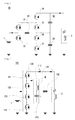
- a DC/DC converter 100 includes a charging and discharging unit 110, a switching unit 120, and an output unit 130.
- the DC/DC converter 100 operates in boost mode in a direction from an input side to an output side, that is, from an input power source 1 to the output unit 130, and operates in buck mode in a direction from the output side to the input side.
- the DC/DC converter 100 according to this embodiment of the present invention enables common grounding because the input power source 1 and the output unit 130 have the same reference electrical potential, and is thus suitable for a dual power supply system for an automobile.
- the charging and discharging unit 110 receives power from the input power source 1 and is charged with the power, or discharges charged power to the output unit 130, thereby transferring energy to the output unit 130.
- the charging and discharging unit 100 includes a charging inductor 111, and a charging capacitor 112 directly connected to the charging inductor 111 and configured such that voltage is stored by a zero current switching (ZCS) method while the inductor current of the charging inductor 111 is forming series resonance.
- ZCS zero current switching
- the switching unit 120 is disposed between the input power source 1 and the charging and discharging unit 110, and allows the charging and discharging unit 110 to be charged with power from the input power source 1 or return power stored therein to the output unit 130.
- the switching unit 120 includes four switching elements.
- the four switching elements include a first switching element 121 configured such that the first terminal thereof is connected to the first terminal of the output unit 130 and the second terminal thereof is connected to the charging inductor 111; a second switching element 122 configured such that the first terminal thereof is connected to the second terminal of the first switching element 121 and the second terminal thereof is connected to the input power source 1; a third switching element 123 configured such that the first terminal thereof is connected to the second terminal of the second switching element 122 and the second terminal thereof is connected to the charging capacitor 112; and a fourth switching element 124 configured such that the first terminal thereof is connected to the second terminal of the third switching element 123 and the second terminal thereof is connected to a ground.
- the output unit 130 receives power stored in the charging and discharging unit 110, and provides output power to a load 2.
- the output unit 130 includes a single capacitor configured to store voltage, and is grounded at the same reference electrical potential as the input power source 1.
- the boost mode of the DC/DC converter 100 will be described in detail with reference to FIG. 5 .
- the second switching element 122 and the fourth switching element 124 are turned on; the input power source 1, the second switching element 122, the charging inductor 111, the charging capacitor 112 and the fourth switching element 124 are connected to each other in the form of a closed loop, and the charging capacitor 112 is charged with an inductor current by a ZCS method while the inductor current is forming series resonance with the charging capacitor 112.
- the inductor current is forming series resonance with the charging capacitor 112
- the inductor current may be expressed by the following Equation 1
- Equation (1) i L is the inductor current, V in is input voltage, v c is the out voltage of the output unit 130, L 1 is the capacity of the charging inductor 111, and C 1 is the capacity of the charging capacitor 112.
- v c t V in - V in - v c t 0 ⁇ cos ⁇ r ⁇ t - t 0
- the second switching element 122 and the fourth switching element 124 are turned off, and the first switching element 121 and the third switching element 123 are turned on.
- the input power source 1, the third switching element 123, the charging capacitor 112, the charging inductor 111, the first switching element 121 and the output unit 130 are connected to each other in the form of a closed loop.
- the voltages of the input power source 1 and the charging capacitor 112 are added to each other and are then supplied to the output unit 130.
- the output unit 130 supplies the boosted power to the load 2.
- Equation 5 the inductor current of the charging inductor 111 is expressed by the following Equation 5 and the capacitor voltage of the charging capacitor 112 is expressed by the following Equation 6:
- i L V in - v c t 1 Z ⁇ sin ⁇ r ⁇ t - t 0 - T s / 2 where T s is the switching period.
- v c t V in - V in - v c t 1 ⁇ cos ⁇ r ⁇ t - t 0 - T s / 2
- V c _max V in + ⁇ ⁇ V c / 2
- V c _min V in - ⁇ ⁇ V c / 2
- Equation 9 the power that the charging capacitor 112 transfers to the output side is expressed by the following Equation 9
- the total power that is transferred to the output side in boost mode may be defined as the sum of the power transferred by the charging capacitor 112 and the power transferred by the input power source 1, as given by the following Equation 11:
- Equation 13 the condition under which the negative voltage does not occur in the charging capacitor 112 is given by the following Equation 13, and the capacitance that satisfies this condition is given by the following Equation 14: ⁇ ⁇ V c ⁇ 2 ⁇ V in C 1 ⁇ 3 R ⁇ f s
- FIG. 6 illustrates the buck mode of the DC/DC converter 100 according to an embodiment of the present invention.
- the first switching element 121 and the third switching element 123 are turned on, the output unit 130, the first switching element 121, the charging inductor 111, the charging capacitor 112 and the third switching element is connected to the input power source 1 in the form of a closed loop, and the inductor current is stored in the charging capacitor 112 by a ZCS method in the form of a voltage while forming series resonance with the charging capacitor 112.
- the capacitor voltage of the charging capacitor 112 corresponds to a voltage obtained by subtracting the voltage of the input power source 1 from the voltage of the output unit 130.
- the first switching element 121 and the third switching element 123 are turned off, the second switching element 122 and the fourth switching element 124 are turned off, the fourth switching element 124, the charging capacitor 112, the charging inductor 111, the second switching element 122 and the input power source 1 are connected in the form of a closed loop, and the voltage with which the charging capacitor 112 has been charged is supplied to the input power source 1.
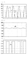
- FIGS. 7 to 12 illustrate simulation waveforms.
- the simulations were conducted under the conditions that the capacity of the charging inductor 111 was set to 0.17 ⁇ H, the capacity of the charging capacitor 112 was set to 22 ⁇ F, the resonance frequency was set to 82.3 kHz, and the switching frequency was set to 80 kHz.
- FIG. 7 illustrates the simulation waveform of the inductor current i L 1 of the charging inductor 111
- FIG. 8 illustrates the simulation waveform of the capacitor voltage V C 1 of the charging capacitor 112 and the simulation waveform of the voltage V in of the input power source 1
- FIG. 9 illustrates the simulation waveforms of the output current I do and load current I o of the DC/DC converter
- FIG. 10 illustrates the simulation waveforms of the voltage V Q 4 and current I Q 4 of the fourth switching element
- FIG. 11 illustrates the simulation waveform of the output power
- FIG. 12 illustrates the simulation waveform of the switching signal of the fourth switching element.
- ZCS zero current switching
- FIG. 13 is a diagram of a DC/DC converter according to another embodiment of the present invention, and illustrates a topology for the parallel driving of a DC/DC converter 100 according to the former embodiment of the present invention.
- the DC/DC converter 200 includes a first charging and discharging unit 210 configured to include a first charging capacitor 212 directly connected to a first charging inductor 211 on the input side thereof; a first switching unit 220 configured to include four switching elements 221, 222, 223 and 224, and to charge the first charging and discharging unit 210 with power from the input power source 1 or return the power to a first output unit 230; a second charging and discharging unit 210' connected in parallel to the first charging and discharging unit 210 and configured to include a second charging inductor 211' and a second charging capacitor 212' directly connected to each other; a second switching unit 220' configured to include four switching elements 221', 222', 223' and 224', and to charge the second charging and discharging unit 210' with power from the input power source 1 or return the power to the first output unit 230; and a first output unit 230 configured to store the voltages of the
- first charging and discharging unit 210 and the second charging and discharging unit 210' perform substantially the same function as the charging and discharging unit 110 of the DC/DC converter 100 according to the former embodiment of the present invention
- first switching unit 220 and the second switching unit 220' perform substantially the same function as the switching unit 120 of the DC/DC converter 100 according to the former embodiment of the present invention.
- the DC/DC converter 200 according to the other embodiment of the present invention is configured such that two DC/DC converters 100 according to the former embodiment of the present invention are connected and form two stages, and performs an interleave operation.
- the DC/DC converter 200 includes an output inductor 240 to charge the output side with power from the first output unit 230 or discharge charged power; a third switching unit 250 configured to charge the output inductor 240 with power from the first output unit 230 or discharge charged power to a second output unit 260, and to include two switching elements 251 and 252; and the second output unit 260 configured to provide the power of the output inductor 240 and the power of the first output unit 230 to a load 2.
- the output side configuration of the DC/DC converter 200 according to the other embodiment of the present invention is substantially the same as that of the conventional bidirectional DC/DC converter 10 having an input/output common ground illustrated in FIG. 1 , and their operations are substantially the same.
- the DC/DC converter 200 has the advantage of enabling parallel driving with high power conversion efficiency because the first and second charging inductors 211 and 211' are connected in series to the input power source 1 when power is transferred to the output side and thus there is no interference of the inductor current upon parallel driving.
- FIG. 14 illustrates a DC/DC converter 300 according to still another embodiment of the present invention.
- a charging and discharging unit 310 includes a charging inductor 311, an arm short protection inductor 312 and a charging capacitor 313, and a switching unit 320 includes a first switching element 321, a second switching element 322, a third switching element 323 and a fourth switching element 324.
- the arm short protection inductor 312 is added compared to the DC/DC converter 100 according to the first embodiment of the present invention.
- the first terminal of the charging inductor 311 is connected to the input power source 1
- the first terminal of the arm short protection inductor 312 is connected to the first terminal of the charging inductor 311
- the first terminal of the charging capacitor 313 is connected to the second terminal of the charging inductor 311 and the second terminal of the charging inductor 311 is connected to the second terminal of the arm short protection inductor 312.
- the first terminal of the first switching element 321 is connected to the first terminal of the output unit; the second switching element 322 connects the second terminal of the charging inductor 311 to the first terminal of the charging capacitor 313, the first terminal of the second switching element 322 is connected to the second terminal of the first switching element 321 and the first terminal of the charging capacitor 313, and the second terminal of the second switching element 322 is connected to the second terminal of the charging inductor 311; the first terminal of the third switching element 323 is connected to the second terminal of the arm short protection inductor 312, and the second terminal of the third switching element 323 is connected to the second terminal of the charging capacitor 313; and the first terminal of the fourth switching element 324 is connected to the second terminal of the third switching element 323 and the second terminal of the charging capacitor 313, and the second terminal of the fourth switching element 324 is grounded.
- the switching unit 320 of the DC/DC converter 300 is configured such that the second switching element 322 is not connected between the input power source 1 and the charging inductor 311 but is connected between the charging inductor 311 and the charging capacitor 313, compared to the switching unit 120 of the DC/DC converter 100 according to the first embodiment of the present invention.
- boost mode when the second switching element 322 and the fourth switching element 323 are turned on, the input power source 1 is directly connected to the charging inductor 311, the second switching element 322, the charging capacitor 313 and the fourth switching element 324 and forms series resonance, and the charging capacitor 313 is charged with the inductor current.
- the first switching element 321 and the third switching element 323 are turned on, the power of the input power source 1 and the charging capacitor 313 is returned and transferred to the output side.
- the DC/DC converter 100 should be provided with a specific dead time when the switching element is interlocked, and the dead time acts as a factor that deteriorates power conversion efficiency when the switching frequency increases.
- the DC/DC converter 100 has the advantages of reducing the risk of the damage of the element and preventing the occurrence of the peak current of the switching element because the arm short protection inductor 312 can buffer the flow of current even when the second switching element 322 and the fourth switching element 323, and the first switching element 321 or the third switching element 323 are simultaneously turned on, and can thus prevent an arm short, thereby eliminating the need for a dead time.
Landscapes
- Engineering & Computer Science (AREA)
- Power Engineering (AREA)
- Dc-Dc Converters (AREA)
Abstract
Description
- The present invention relates generally to a bidirectional direct current DC/DC converter and, more particularly, to a resonant bidirectional DC/DC converter, in which the input and output thereof are grounded in common to the chassis of a vehicle at the same input and output electrical potential and then double boost can be achieved, and in which a resonance destruction phenomenon, attributable to interference between inductor currents during parallel driving for quadruple boost, does not occur and thus an increase in output is facilitated, thereby being applied to a dual power supply system for a vehicle.
- Recently, as a need for high fuel efficiency has increased because of a concern about global warming, research has been actively conducted into stop-start system technology in which the operation of an engine is stopped during the no-load operation of a vehicle in an automobile system in order to reduce the consumption of energy.
- Since the fuel consumed by the no-load operation of a vehicle amounts to about 5-8% of the total fuel consumed, a stop-start system is necessarily applied to hybrid vehicles, and also the application of the system to general internal combustion engine vehicles is extending.
- In general, stop-start systems necessarily employ an engine starting motor operating at a high voltage in order to maximize efficiency, and a 48-V voltage system is constructed in order to operate the engine starting motor.
- Accordingly, in the case of hybrid vehicles, a dual power supply system has been introduced in which an existing 12 V voltage system is employed for a low-level power demand, such as a demand for lighting, and a 48 V voltage system is constructed for a high-level power demand, such as a demand for a start system, a power steering system, and an air-conditioning and heating system.
- The same grounding is essential because a dual voltage system requires that input and output power sources are grounded in common to the chassis of a vehicle due to the characteristics of a vehicle electrical system, and an increase in the efficiency of a DC/DC converter is also essential because high boost, such as quadruple boost, is required.
-
FIG. 1 is a diagram illustrating a conventional bidirectional DC/DC converter 10 having an input and output common ground. Referring toFIG. 1 , the conventional bidirectional DC/DC converter 10 having an input and output common ground includes aninductor 11 configured to perform the charging and discharging of power from aninput power source 1; acharging switch 13 configured to connect the output terminal of theinductor 11 to a ground, and to allow theinductor 11 to be charged with the power from theinput power source 1; areturn switch 12 configured to return the power stored in theinductor 11 to an output side; and anoutput capacitor 14 configured to receive the power from theinput power source 1 and the power stored in theinductor 11, and to supply output power to aload 2. - Furthermore, when the
charging switch 13 and thereturn switch 12 are implemented as MOSFET switch elements, they are interlocked with each other and perform ON and OFF operations in order to reduce the saturated voltage of diodes, and act as buck capacitors in a direction from theoutput capacitor 14 to theinput power source 1. - However, the conventional bidirectional DC/
DC converter 10 having an input and output common ground is limited in implementation as a high-efficiency power converter because when it operates as a quadruple or higher boost converter, the time it takes to transfer power to an output side is reduced due to the high time ratio of the switch. -
FIG. 2 is a diagram illustrating a conventional double boost-enabled soft switching-type bidirectional DC/DC converter 20. Referring toFIG. 2 , the conventional double boost-enabled soft switching-type bidirectional DC/DC converter 20 includes aninductor 21 directly connected to aninput power source 1, and configured to perform the charging and discharging of input power; afirst output capacitor 26 and asecond output capacitor 27 connected in series to each other; afirst switch 22 and athird switch 24 configured to supply the current of theinductor 21 to thefirst output capacitor 26 and then charge thefirst output capacitor 26 through series resonance; and asecond switch 23 and afourth switch 25 configured to operate in the state of being interlocked with thefirst switch 22 and thethird switch 24, and to supply the current of theinductor 21 to thesecond output capacitor 27 and then charge thesecond output capacitor 27 through series resonance. - However, the conventional double boost-enabled soft switching-type bidirectional DC/
DC converter 20 is problematic in that it cannot be used in cases, such as a vehicle in which all power sources are grounded to a vehicle frame, because the reference electrical potential of theinput power source 1 is different from the reference electrical potential of theoutput capacitors - Furthermore, the conventional double boost-enabled soft switching-type bidirectional DC/
DC converter 20 has a structure incapable of parallel driving for an increase in current capacity because the two output capacitors are connected to an output, and inductor currents interfere with each other upon parallel driving, and thus a phenomenon of resonance destruction occurs. -
FIG. 3 is a diagram illustrating a conventional double boost-enabled identical electrical potential-type DC/DC converter 30. Referring toFIG. 3 , the conventional double boost-enabled identical electrical potential-type DC/DC converter 30 is configured such that in order to form the same reference electrical potential, a 1-1switch 31, a 1-2switch 32 and an input formation capacitor 33 are added to the input side of the conventional double boost-enabled soft switching-type bidirectional DC/DC converter 20 illustrated inFIG. 2 . - That is, the conventional double boost-enabled identical electrical potential-type DC/
DC converter 30 is configured such that the input formation capacitor 33 is charged with the power from theinput power source 1 by the 1-1switch 31 and the 1-2switch 32 and theoutput capacitors - As the result of efforts to research and develop a DC/DC converter suitable for a dual power supply system, the inventors have attained a DC/DC converter in which common grounding can be achieved because input and output electrical potentials are the same, the efficiency of power conversion can be improved because switching loss is reduced using a zero current switching (ZCS) method, and charging can be performed through series resonance during parallel driving without the interference of a resonance circuit, thereby contriving the present invention.
- Accordingly, an object of the present invention is to provide a DC/DC converter that is suitable for a dual power supply system for a vehicle because input and output electrical potentials are the same and thus common grounding is possible.
- Another object of the present invention is to provide a DC/DC converter that is capable of soft switching across an overall range and also capable of power conversion using a low-capacity inductor.
- Still another object of the present invention is to provide a DC/DC converter that is capable of easily increasing current capacity because interference does not occur upon parallel driving.
- Objects of the present invention are not limited to the above-described objects, and other objects that have not been described above will be clearly understood by those skilled in the art from the following description.
- In accordance with an aspect of the present invention, there is provided a direct current DC/DC converter, including, in boost mode, a charging and discharging unit configured to perform charging and discharging of input power; a switching unit provided between an input power source and the charging and discharging unit, and configured to charge the charging and discharging unit with the input power or return power stored in the charging and discharging unit to an output side; and an output unit connected to the output side of the charging and discharging unit, and configured to receive the input power and the power stored in the charging and discharging unit and provide output power; wherein the output unit and the input power are grounded in common at an identical electrical potential.
- In buck mode, the charging and discharging unit may be charged with the output power of the output unit and discharge the stored power to the input power; the switching unit may allow the output power of the output unit to be divided into the input power and to be stored in the charging and discharging unit, or may allow the power stored in the charging and discharging unit to be discharged to the input power; and the DC/DC converter may operate in boost mode in a direction from the input side to the output side and in buck mode in a direction from the output side and the input side, thereby enabling bidirectional power transmission.
- The charging and discharging unit may include a charging inductor, and a charging capacitor configured such that a first terminal thereof is connected to a first terminal of the charging inductor and a voltage is stored therein while an inductor current is forming series resonance; the switching unit may include a first switching element configured such that the first terminal thereof is connected to the first terminal of the output unit, a second switching element configured such that the first terminal thereof is connected to the second terminal of the first switching element and the second terminal thereof is connected to the input power source, a third switching element configured such that a first terminal thereof is connected to a second terminal of the second switching element, and a fourth switching element configured such that a first terminal thereof is connected to a second terminal of the third switching element and a second terminal thereof is grounded; a second terminal of the charging inductor is connected between the first switching element and the second switching element, and a second terminal of the charging capacitor is connected between the third switching element and the fourth switching element; and the first switching element and the third switching element are interlocked with the second switching element and the fourth switching element and are selectively turned on and off.
- In boost mode, when the second switching element and the fourth switching element are turned on, the input power, the charging inductor and the charging capacitor are sequentially connected and form a closed loop, the inductor current forms series resonance and the charging capacitor is charged with a voltage by a zero current switching method; and, when the first switching element and the third switching element are turned on, the input power, the charging capacitor, the charging inductor and the output unit are sequentially connected and form a closed loop, and the power stored in the charging capacitor is added to the input power and is supplied to the output unit.
- In buck mode, when the first switching element and the third switching element are turned on, the output unit, the charging inductor, the charging capacitor and the input power are sequentially connected and form a closed loop, and the charging capacitor is charged with a voltage by a zero current switching method, the voltage corresponding to a voltage obtained by subtracting the input power from the output power of the output unit; and, when the second switching element and the fourth switching element are turned on, the charging capacitor, the charging inductor and the input power are sequentially connected and form a closed loop, and the power stored in the charging inductor is supplied to the input power.
- The charging and discharging unit may include a charging inductor configured such that a first terminal thereof is connected to the input power source, an arm short protection inductor configured such that a first terminal thereof is connected to a first terminal of the charging inductor, and configured to prevent arm short of the switching unit, and a charging capacitor configured such that a first terminal thereof is connected to a second terminal of the charging inductor and a second terminal thereof is connected to a second terminal of the arm short protection inductor; the switching unit may include a first switching element configured such that a first terminal thereof is connected to a first terminal of the output unit, a second switching element configured to connect a second terminal of the charging inductor to a first terminal of the charging capacitor, and configured such that a first terminal of the second switching element is connected to a second terminal of the first switching element and a first terminal of the charging capacitor and a second terminal of the second switching element is connected to a second terminal of the charging inductor, a third switching element such that a first terminal thereof is connected to a second terminal of the arm short protection inductor and a second terminal thereof is connected to a second terminal of the charging capacitor, and a fourth switching element configured such that a first terminal thereof is connected to a second terminal of the third switching element and a second terminal of the charging capacitor and a second terminal thereof is grounded; and the first switching element and the third switching element are interlocked with the second switching element and the fourth switching element and are selectively turned on and off.
- In accordance with another aspect of the present invention, there is provided a direct current DC/DC converter, including a first charging and discharging unit configured to perform charging and discharging of input power; a first switching unit provided between an input power source and the first charging and discharging unit, and configured to charge the first charging and discharging unit with the input power or return power stored in the first charging and discharging unit to an output side; a second charging and discharging unit connected in parallel with the first charging and discharging unit, and to perform charging and discharging of the input power; a second switching unit provided between the input power and the second charging and discharging unit, and configured to allow the second charging and discharging unit to be charged with the input power or return power stored in the second charging and discharging unit to a first output unit; the first output unit connected to the first charging and discharging unit and the second charging and discharging unit, and configured to receive and store power of the first charging and discharging unit and the second charging and discharging unit; an output inductor connected to the first output unit, and configured to perform charging and discharging of power of the first output unit; a third switching unit configured to make the output inductor grounded, and to charge the output inductor or return the power stored in the output inductor to a second output unit; and the second output unit connected to the third switching unit, and configured to receive the power of the first output unit and the output inductor and provide output power; wherein the input power, the first output unit and the second output unit are grounded in common at an identical electrical potential.
- The first charging and discharging unit may include a first charging inductor, and a first charging capacitor configured such that a first terminal thereof is connected to a first terminal of the first charging inductor and a voltage is stored therein while an inductor current is forming series resonance; the first switching unit may include a 1-1 switching element configured such that a first terminal thereof is connected to a first terminal of the first output unit, a 1-2 switching element configured such that a first terminal thereof is connected to a second terminal of the 1-1 switching element and the second terminal thereof is connected to the input power source, a 1-3 switching element configured such that a first terminal thereof is connected to a second terminal of the 1-2 switching element, and a 1-4 switching element configured such that a first terminal thereof is connected to a second terminal of the 1-3 switching element and a second terminal thereof is grounded; the second switching unit may include a 2-1 switching element configured such that a first terminal thereof is connected to a first terminal of the first output unit, a 2-2 switching element configured such that a first terminal thereof is connected to a second terminal of the 2-1 switching element and the second terminal thereof is connected to the input power source, a 2-3 switching element configured such that a first terminal thereof is connected to a second terminal of the 2-2 switching element, and a 2-4 switching element configured such that a first terminal thereof is connected to a second terminal of the 2-3 switching element and a second terminal thereof is grounded; a second terminal of the second charging inductor is connected between the 2-1 switching element and the 2-2 switching element, and a second terminal of the second charging capacitor is connected between the 2-3 switching element and the 2-4 switching element; and the 1-1 switching element, the 1-3 switching element, the 2-1 switching element and the 2-3 switching element are interlocked with the 1-2 switching element, the 1-4 switching element, the 2-2 switching element and the 2-4 switching element, and are selectively turned on and off.
- The above and other objects, features and advantages of the present invention will be more clearly understood from the following detailed description taken in conjunction with the accompanying drawings, in which:
-
FIG. 1 is a diagram illustrating a conventional bidirectional DC/DC converter having an input and output common ground; -
FIG. 2 is a diagram illustrating a conventional double boost-enabled soft switching-type bidirectional DC/DC converter; -
FIG. 3 is a diagram illustrating a conventional double boost-enabled identical electrical potential-type DC/DC converter; -
FIG. 4 is a diagram illustrating a DC/DC converter according to an embodiment of the present invention; -
FIG. 5 is a diagram illustrating the boost mode of the DC/DC converter according to the embodiment of the present invention; -
FIG. 6 is a diagram illustrating the buck mode of the DC/DC converter according to the embodiment of the present invention; -
FIGS. 7 to 12 are diagrams illustrating the simulation waveforms of the DC/DC converter according to the embodiment of the present invention; -
FIG. 13 is a diagram illustrating a DC/DC converter according to another embodiment of the present invention; and -
FIG. 14 is a diagram illustrating a DC/DC converter according to still another embodiment of the present invention. - Although general terms widely used currently are selected as the terms used herein as much as possible, the terms selected by the applicant as desired are also used in specific cases. In these cases, the meanings of the terms should be interpreted based on the meanings used and described in the following detailed description, rather than simply based on the names of the terms.
- The technical configuration of the present invention will be described in detail with reference to embodiments illustrated in the accompanying diagrams.
- However, the present invention is not limited to the described embodiments, and may be implemented in different forms. Throughout the specification, the same reference numerals designate the same or like components.
- Referring to
FIG. 4 , a DC/DC converter 100 according to an embodiment of the present invention includes a charging anddischarging unit 110, aswitching unit 120, and anoutput unit 130. - Furthermore, the DC/
DC converter 100 according to this embodiment of the present invention operates in boost mode in a direction from an input side to an output side, that is, from aninput power source 1 to theoutput unit 130, and operates in buck mode in a direction from the output side to the input side. - Furthermore, the DC/
DC converter 100 according to this embodiment of the present invention enables common grounding because theinput power source 1 and theoutput unit 130 have the same reference electrical potential, and is thus suitable for a dual power supply system for an automobile. - The charging and discharging
unit 110 receives power from theinput power source 1 and is charged with the power, or discharges charged power to theoutput unit 130, thereby transferring energy to theoutput unit 130. - Furthermore, the charging and discharging
unit 100 includes acharging inductor 111, and acharging capacitor 112 directly connected to thecharging inductor 111 and configured such that voltage is stored by a zero current switching (ZCS) method while the inductor current of thecharging inductor 111 is forming series resonance. - The
switching unit 120 is disposed between theinput power source 1 and the charging and dischargingunit 110, and allows the charging and dischargingunit 110 to be charged with power from theinput power source 1 or return power stored therein to theoutput unit 130. - Furthermore, the
switching unit 120 includes four switching elements. The four switching elements include afirst switching element 121 configured such that the first terminal thereof is connected to the first terminal of theoutput unit 130 and the second terminal thereof is connected to thecharging inductor 111; asecond switching element 122 configured such that the first terminal thereof is connected to the second terminal of thefirst switching element 121 and the second terminal thereof is connected to theinput power source 1; athird switching element 123 configured such that the first terminal thereof is connected to the second terminal of thesecond switching element 122 and the second terminal thereof is connected to thecharging capacitor 112; and afourth switching element 124 configured such that the first terminal thereof is connected to the second terminal of thethird switching element 123 and the second terminal thereof is connected to a ground. - The
output unit 130 receives power stored in the charging and dischargingunit 110, and provides output power to aload 2. - Furthermore, the
output unit 130 includes a single capacitor configured to store voltage, and is grounded at the same reference electrical potential as theinput power source 1. - The boost mode of the DC/
DC converter 100 according to an embodiment of the present invention will be described in detail with reference toFIG. 5 . - Referring to
FIG. 5A , in boost mode, thesecond switching element 122 and thefourth switching element 124 are turned on; theinput power source 1, thesecond switching element 122, thecharging inductor 111, thecharging capacitor 112 and thefourth switching element 124 are connected to each other in the form of a closed loop, and thecharging capacitor 112 is charged with an inductor current by a ZCS method while the inductor current is forming series resonance with thecharging capacitor 112. - Furthermore, while the inductor current is forming series resonance with the charging
capacitor 112, the inductor current may be expressed by the followingEquation 1 and the capacitor voltage of the chargingcapacitor 112 may be expressed by the following Equation 2:
- In Equation (1), iL is the inductor current, Vin is input voltage, vc is the out voltage of the
output unit 130, L 1 is the capacity of the charginginductor 111, and C 1 is the capacity of the chargingcapacitor 112.
- Furthermore, the
output unit 130 is responsible for the output current output to the load, in which case a variation in output voltage is expressed by the following Equation 3:
where V 0 is the voltage of theoutput unit 130, R is the load, C 0 is the capacitance of theoutput unit 130, and fs is the series resonance frequency. - Accordingly, when the ripple factor of the output voltage is determined, the capacitance of the
output unit 130 corresponding to the ripple factor is determined by the following Equation 4:
- Next, referring to
FIG. 5B , thesecond switching element 122 and thefourth switching element 124 are turned off, and thefirst switching element 121 and thethird switching element 123 are turned on. In this case, theinput power source 1, thethird switching element 123, the chargingcapacitor 112, the charginginductor 111, thefirst switching element 121 and theoutput unit 130 are connected to each other in the form of a closed loop. The voltages of theinput power source 1 and the chargingcapacitor 112 are added to each other and are then supplied to theoutput unit 130. Theoutput unit 130 supplies the boosted power to theload 2. - In this case, the inductor current of the charging
inductor 111 is expressed by the followingEquation 5 and the capacitor voltage of the chargingcapacitor 112 is expressed by the following Equation 6:

- Furthermore, the voltage average value of the charging
capacitor 112 is the input voltage, and the maximum voltage and the minimum voltage are expressed by the following Equation 7:
- Accordingly, a variation in the energy of the charging
capacitor 112 is expressed by the following Equation 8:
- Furthermore, the power that the charging
capacitor 112 transfers to the output side is expressed by the following Equation 9, and the power that theinput power source 1 transfers to the output side is expressed by the following Equation 10:

- Accordingly, the total power that is transferred to the output side in boost mode may be defined as the sum of the power transferred by the charging
capacitor 112 and the power transferred by theinput power source 1, as given by the following Equation 11:
- Furthermore, when power conversion loss is negligible, it can be assumed that the power transferred from the input side to the output side is the same as the power consumption of the output side, and thus the voltage ripple of the charging
capacitor 112 can be defined as the following Equation 12:
- Furthermore, the condition under which the negative voltage does not occur in the charging
capacitor 112 is given by the followingEquation 13, and the capacitance that satisfies this condition is given by the following Equation 14:

-
FIG. 6 illustrates the buck mode of the DC/DC converter 100 according to an embodiment of the present invention. Referring toFIG. 6A , in buck mode, thefirst switching element 121 and thethird switching element 123 are turned on, theoutput unit 130, thefirst switching element 121, the charginginductor 111, the chargingcapacitor 112 and the third switching element is connected to theinput power source 1 in the form of a closed loop, and the inductor current is stored in the chargingcapacitor 112 by a ZCS method in the form of a voltage while forming series resonance with the chargingcapacitor 112. - Furthermore, the capacitor voltage of the charging
capacitor 112 corresponds to a voltage obtained by subtracting the voltage of theinput power source 1 from the voltage of theoutput unit 130. - Furthermore, Referring to
FIG. 6B , thefirst switching element 121 and thethird switching element 123 are turned off, thesecond switching element 122 and thefourth switching element 124 are turned off, thefourth switching element 124, the chargingcapacitor 112, the charginginductor 111, thesecond switching element 122 and theinput power source 1 are connected in the form of a closed loop, and the voltage with which the chargingcapacitor 112 has been charged is supplied to theinput power source 1. -
FIGS. 7 to 12 illustrate simulation waveforms. The simulations were conducted under the conditions that the capacity of the charginginductor 111 was set to 0.17 µH, the capacity of the chargingcapacitor 112 was set to 22 µF, the resonance frequency was set to 82.3 kHz, and the switching frequency was set to 80 kHz. - Furthermore,
FIG. 7 illustrates the simulation waveform of the inductor current i L1 of the charginginductor 111,FIG. 8 illustrates the simulation waveform of the capacitor voltage V C1 of the chargingcapacitor 112 and the simulation waveform of the voltage Vin of theinput power source 1,FIG. 9 illustrates the simulation waveforms of the output current Ido and load current Io of the DC/DC converter,FIG. 10 illustrates the simulation waveforms of the voltage V Q4 and current I Q4 of the fourth switching element,FIG. 11 illustrates the simulation waveform of the output power, andFIG. 12 illustrates the simulation waveform of the switching signal of the fourth switching element. - Referring to
FIGS. 7 and12 , since the resonance circuit having a resonance frequency of 82.3 kHz applied a switching signal of 80.0 kHz, regions 'a' in which the resonance current was discontinuous were present. Referring toFIGS. 7 and 8 , the difference in phase between the charging voltage V C1 and the inductor current i L1 of thecapacitor 112 was 90 degrees, and the voltage ripple was 0.1 V. - Furthermore, referring to
FIG. 9 , the output current Ido appeared in the form of an approximate sine wave half-wave rectified waveform, and the peak value thereof is given as the following Equation 15:
- Furthermore, from
FIGS. 10 and 12 , it can be seen that zero current switching (ZCS) was performed when the switching element was turned on and off. - Furthermore, from
FIG. 11 , it can be seen that a ripple of 0.1 occurred with respect to an average output of about 192 W and thus extremely desired output was achieved. -
FIG. 13 is a diagram of a DC/DC converter according to another embodiment of the present invention, and illustrates a topology for the parallel driving of a DC/DC converter 100 according to the former embodiment of the present invention. - Referring to
FIG. 13 , the DC/DC converter 200 according to another embodiment of the present invention includes a first charging and dischargingunit 210 configured to include afirst charging capacitor 212 directly connected to afirst charging inductor 211 on the input side thereof; afirst switching unit 220 configured to include four switchingelements unit 210 with power from theinput power source 1 or return the power to afirst output unit 230; a second charging and discharging unit 210' connected in parallel to the first charging and dischargingunit 210 and configured to include a second charging inductor 211' and a second charging capacitor 212' directly connected to each other; a second switching unit 220' configured to include four switching elements 221', 222', 223' and 224', and to charge the second charging and discharging unit 210' with power from theinput power source 1 or return the power to thefirst output unit 230; and afirst output unit 230 configured to store the voltages of the first charging and dischargingunit 210 and the second charging and discharging unit 210'. - Furthermore, the first charging and discharging
unit 210 and the second charging and discharging unit 210' perform substantially the same function as the charging and dischargingunit 110 of the DC/DC converter 100 according to the former embodiment of the present invention, and thefirst switching unit 220 and the second switching unit 220' perform substantially the same function as theswitching unit 120 of the DC/DC converter 100 according to the former embodiment of the present invention. - That is, the DC/
DC converter 200 according to the other embodiment of the present invention is configured such that two DC/DC converters 100 according to the former embodiment of the present invention are connected and form two stages, and performs an interleave operation. - The DC/
DC converter 200 according to the other embodiment of the present invention includes anoutput inductor 240 to charge the output side with power from thefirst output unit 230 or discharge charged power; athird switching unit 250 configured to charge theoutput inductor 240 with power from thefirst output unit 230 or discharge charged power to asecond output unit 260, and to include two switchingelements second output unit 260 configured to provide the power of theoutput inductor 240 and the power of thefirst output unit 230 to aload 2. - That is, the output side configuration of the DC/
DC converter 200 according to the other embodiment of the present invention is substantially the same as that of the conventional bidirectional DC/DC converter 10 having an input/output common ground illustrated inFIG. 1 , and their operations are substantially the same. - Furthermore, the DC/
DC converter 200 according to the other embodiment of the present invention has the advantage of enabling parallel driving with high power conversion efficiency because the first andsecond charging inductors 211 and 211' are connected in series to theinput power source 1 when power is transferred to the output side and thus there is no interference of the inductor current upon parallel driving. - Furthermore,
FIG. 14 illustrates a DC/DC converter 300 according to still another embodiment of the present invention. Referring toFIG. 14 , in the DC/DC converter 300 according to this embodiment of the present invention, a charging and dischargingunit 310 includes a charginginductor 311, an armshort protection inductor 312 and a chargingcapacitor 313, and aswitching unit 320 includes afirst switching element 321, asecond switching element 322, athird switching element 323 and afourth switching element 324. - That is, the arm
short protection inductor 312 is added compared to the DC/DC converter 100 according to the first embodiment of the present invention. - Furthermore, the first terminal of the charging
inductor 311 is connected to theinput power source 1, the first terminal of the armshort protection inductor 312 is connected to the first terminal of the charginginductor 311, and the first terminal of the chargingcapacitor 313 is connected to the second terminal of the charginginductor 311 and the second terminal of the charginginductor 311 is connected to the second terminal of the armshort protection inductor 312. - Furthermore, the first terminal of the
first switching element 321 is connected to the first terminal of the output unit; thesecond switching element 322 connects the second terminal of the charginginductor 311 to the first terminal of the chargingcapacitor 313, the first terminal of thesecond switching element 322 is connected to the second terminal of thefirst switching element 321 and the first terminal of the chargingcapacitor 313, and the second terminal of thesecond switching element 322 is connected to the second terminal of the charginginductor 311; the first terminal of thethird switching element 323 is connected to the second terminal of the armshort protection inductor 312, and the second terminal of thethird switching element 323 is connected to the second terminal of the chargingcapacitor 313; and the first terminal of thefourth switching element 324 is connected to the second terminal of thethird switching element 323 and the second terminal of the chargingcapacitor 313, and the second terminal of thefourth switching element 324 is grounded. - That is, the
switching unit 320 of the DC/DC converter 300 according to this embodiment of the present invention is configured such that thesecond switching element 322 is not connected between theinput power source 1 and the charginginductor 311 but is connected between the charginginductor 311 and the chargingcapacitor 313, compared to theswitching unit 120 of the DC/DC converter 100 according to the first embodiment of the present invention. - Furthermore, in boost mode, when the
second switching element 322 and thefourth switching element 323 are turned on, theinput power source 1 is directly connected to the charginginductor 311, thesecond switching element 322, the chargingcapacitor 313 and thefourth switching element 324 and forms series resonance, and the chargingcapacitor 313 is charged with the inductor current. When thefirst switching element 321 and thethird switching element 323 are turned on, the power of theinput power source 1 and the chargingcapacitor 313 is returned and transferred to the output side. - Meanwhile, when the
first switching element 321 and thethird switching element 323 are interlocked with thesecond switching element 322 and thefourth switching element 323, thesecond switching element 322 and thefourth switching element 323, and thefirst switching element 321 or thethird switching element 323 are simultaneously turned on, and thus an arm short phenomenon in which a plus terminal and a minus terminal are directly connected may occur. Since this arm short phenomenon may cause the damage of an element attributable to a peak current, the DC/DC converter 100 according to the first embodiment of the present invention should be provided with a specific dead time when the switching element is interlocked, and the dead time acts as a factor that deteriorates power conversion efficiency when the switching frequency increases. - In contrast, the DC/
DC converter 100 according to this embodiment of the present invention has the advantages of reducing the risk of the damage of the element and preventing the occurrence of the peak current of the switching element because the armshort protection inductor 312 can buffer the flow of current even when thesecond switching element 322 and thefourth switching element 323, and thefirst switching element 321 or thethird switching element 323 are simultaneously turned on, and can thus prevent an arm short, thereby eliminating the need for a dead time. - The present invention has the following advantages:
- First, the DC/DC converter according to at least one embodiment of the present invention has the advantage of being suitably applied to a dual power supply system for a vehicle because the input and the output are grounded in common and, thus, soft switching is enabled across an overall range and power conversion is also enabled using a low-capacity inductor.
- Furthermore, the DC/DC converter according to at least one embodiment of the present invention has the advantages of easily increasing current capacity and power conversion efficiency because the charging inductor is connected in series to the input power upon parallel driving and, thus, interference does not occur between the resonance circuits.
- Although the preferred embodiments of the present invention have been disclosed for illustrative purposes, those skilled in the art will appreciate that various modifications, additions and substitutions are possible, without departing from the scope and spirit of the invention as disclosed in the accompanying claims.
Claims (8)
- A direct current DC/DC converter, comprising:in boost mode:a charging and discharging unit configured to perform charging and discharging of input power;a switching unit provided between an input power source and the charging and discharging unit, and configured to charge the charging and discharging unit with the input power or return power stored in the charging and discharging unit to an output side; andan output unit connected to an output side of the charging and discharging unit, and configured to receive the input power and the power stored in the charging and discharging unit and provide output power;wherein the output unit and the input power are grounded in common at an identical electrical potential.
- The DC/DC converter of claim 1, wherein:in buck mode:the charging and discharging unit is charged with the output power of the output unit and discharges the stored power to the input power;the switching unit allows the output power of the output unit to be divided into the input power and to be stored in the charging and discharging unit, or allows the power stored in the charging and discharging unit to be discharged to the input power; andthe DC/DC converter operates in boost mode in a direction from the input side to the output side and in buck mode in a direction from the output side and the input side, thereby enabling bidirectional power transmission.
- The DC/DC converter of claim 1 or 2, wherein:the charging and discharging unit comprises:a charging inductor, anda charging capacitor configured such that a first terminal thereof is connected to a first terminal of the charging inductor and a voltage is stored therein while an inductor current is forming series resonance;the switching unit comprises:a first switching element configured such that a first terminal thereof is connected to a first terminal of the output unit,a second switching element configured such that a first terminal thereof is connected to a second terminal of the first switching element and a second terminal thereof is connected to the input power source,a third switching element configured such that a first terminal thereof is connected to a second terminal of the second switching element, anda fourth switching element configured such that a first terminal thereof is connected to a second terminal of the third switching element and a second terminal thereof is grounded;a second terminal of the charging inductor is connected between the first switching element and the second switching element, and a second terminal of the charging capacitor is connected between the third switching element and the fourth switching element; andthe first switching element and the third switching element are interlocked with the second switching element and the fourth switching element and are selectively turned on and off.
- The DC/DC converter of claim 3, wherein:in boost mode:when the second switching element and the fourth switching element are turned on, the input power, the charging inductor and the charging capacitor are sequentially connected and form a closed loop, the inductor current forms series resonance and the charging capacitor is charged with a voltage by a zero current switching method; andwhen the first switching element and the third switching element are turned on, the input power, the charging capacitor, the charging inductor and the output unit are sequentially connected and form a closed loop, and the power stored in the charging capacitor is added to the input power and is supplied to the output unit.
- The DC/DC converter of claim 4, wherein:in buck mode:when the first switching element and the third switching element are turned on, the output unit, the charging inductor, the charging capacitor and the input power are sequentially connected and form a closed loop, and the charging capacitor is charged with a voltage by a zero current switching method, the voltage corresponding to a voltage obtained by subtracting the input power from the output power of the output unit; andwhen the second switching element and the fourth switching element are turned on, the charging capacitor, the charging inductor and the input power are sequentially connected and form a closed loop, and the power stored in the charging inductor is supplied to the input power.
- The DC/DC converter of claim 1, wherein:the charging and discharging unit comprises:a charging inductor configured such that a first terminal thereof is connected to the input power source,an arm short protection inductor configured such that a first terminal thereof is connected to a first terminal of the charging inductor, and configured to prevent arm short of the switching unit, anda charging capacitor configured such that a first terminal thereof is connected to a second terminal of the charging inductor and a second terminal thereof is connected to a second terminal of the arm short protection inductor;the switching unit comprises:a first switching element configured such that a first terminal thereof is connected to a first terminal of the output unit,a second switching element configured to connect a second terminal of the charging inductor to a first terminal of the charging capacitor, and configured such that a first terminal of the second switching element is connected to a second terminal of the first switching element and a first terminal of the charging capacitor and a second terminal of the second switching element is connected to a second terminal of the charging inductor,a third switching element such that a first terminal thereof is connected to a second terminal of the arm short protection inductor and a second terminal thereof is connected to a second terminal of the charging capacitor, anda fourth switching element configured such that a first terminal thereof is connected to a second terminal of the third switching element and a second terminal of the charging capacitor and a second terminal thereof is grounded; andthe first switching element and the third switching element are interlocked with the second switching element and the fourth switching element and are selectively turned on and off.
- A direct current DC/DC converter, comprising:a first charging and discharging unit configured to perform charging and discharging of input power;a first switching unit provided between an input power source and the first charging and discharging unit, and configured to charge the first charging and discharging unit with the input power or return power stored in the first charging and discharging unit to an output side;a second charging and discharging unit connected in parallel with the first charging and discharging unit, and to perform charging and discharging of the input power;a second switching unit provided between the input power and the second charging and discharging unit, and configured to allow the second charging and discharging unit to be charged with the input power or return power stored in the second charging and discharging unit to a first output unit;the first output unit connected to the first charging and discharging unit and the second charging and discharging unit, and configured to receive and store power of the first charging and discharging unit and the second charging and discharging unit;an output inductor connected to the first output unit, and configured to perform charging and discharging of power of the first output unit;a third switching unit configured to make the output inductor grounded, and to charge the output inductor or return the power stored in the output inductor to a second output unit; andthe second output unit connected to the third switching unit, and configured to receive the power of the first output unit and the output inductor and provide output power;wherein the input power, the first output unit and the second output unit are grounded in common at an identical electrical potential.
- The DC/DC converter of claim 7, wherein:the first charging and discharging unit comprises:a first charging inductor, anda first charging capacitor configured such that a first terminal thereof is connected to a first terminal of the first charging inductor and a voltage is stored therein while an inductor current is forming series resonance;the first switching unit comprises:a 1-1 switching element configured such that a first terminal thereof is connected to a first terminal of the first output unit,a 1-2 switching element configured such that a first terminal thereof is connected to a second terminal of the 1-1 switching element and the second terminal thereof is connected to the input power source,a 1-3 switching element configured such that a first terminal thereof is connected to a second terminal of the 1-2 switching element, anda 1-4 switching element configured such that a first terminal thereof is connected to a second terminal of the 1-3 switching element and a second terminal thereof is grounded;the second switching unit comprises:a 2-1 switching element configured such that a first terminal thereof is connected to a first terminal of the first output unit,a 2-2 switching element configured such that a first terminal thereof is connected to a second terminal of the 2-1 switching element and the second terminal thereof is connected to the input power source,a 2-3 switching element configured such that a first terminal thereof is connected to a second terminal of the 2-2 switching element, anda 2-4 switching element configured such that a first terminal thereof is connected to a second terminal of the 2-3 switching element and a second terminal thereof is grounded;a second terminal of the second charging inductor is connected between the 2-1 switching element and the 2-2 switching element, and a second terminal of the second charging capacitor is connected between the 2-3 switching element and the 2-4 switching element; andthe 1-1 switching element, the 1-3 switching element, the 2-1 switching element and the 2-3 switching element are interlocked with the 1-2 switching element, the 1-4 switching element, the 2-2 switching element and the 2-4 switching element, and are selectively turned on and off.
Applications Claiming Priority (1)
| Application Number | Priority Date | Filing Date | Title |
|---|---|---|---|
| KR1020130073903A KR101395569B1 (en) | 2013-06-26 | 2013-06-26 | Resonant dc/dc converter using the source |
Publications (3)
| Publication Number | Publication Date |
|---|---|
| EP2819290A2 true EP2819290A2 (en) | 2014-12-31 |
| EP2819290A3 EP2819290A3 (en) | 2015-04-08 |
| EP2819290B1 EP2819290B1 (en) | 2017-08-23 |
Family
ID=50894240
Family Applications (1)
| Application Number | Title | Priority Date | Filing Date |
|---|---|---|---|
| EP14173842.7A Not-in-force EP2819290B1 (en) | 2013-06-26 | 2014-06-25 | Resonant bidirectional DC/DC converter with the same input and output electrical potential |
Country Status (2)
| Country | Link |
|---|---|
| EP (1) | EP2819290B1 (en) |
| KR (1) | KR101395569B1 (en) |
Cited By (2)
| Publication number | Priority date | Publication date | Assignee | Title |
|---|---|---|---|---|
| KR20170072234A (en) * | 2014-10-02 | 2017-06-26 | 메루스 오디오 에이피에스 | A multiple output boost dc-dc power converter |
| US10778105B2 (en) | 2017-12-11 | 2020-09-15 | Ford Global Technologies, Llc | Interleaved DC-DC converter for electrified vehicles |
Families Citing this family (1)
| Publication number | Priority date | Publication date | Assignee | Title |
|---|---|---|---|---|
| CN108347167B (en) | 2017-01-25 | 2021-07-13 | 通用电气公司 | System and method for soft-switching DC-DC converters |
Family Cites Families (8)
| Publication number | Priority date | Publication date | Assignee | Title |
|---|---|---|---|---|
| US5657219A (en) * | 1995-08-29 | 1997-08-12 | Crown International, Inc. | Opposed current power converter |
| US6984967B2 (en) | 2003-10-29 | 2006-01-10 | Allegro Microsystems, Inc. | Multi-mode switching regulator |
| US7466112B2 (en) | 2005-02-08 | 2008-12-16 | Linear Technology Corporation | Variable frequency current-mode control for switched step up-step down regulators |
| JP4768498B2 (en) * | 2006-04-14 | 2011-09-07 | 日立コンピュータ機器株式会社 | Bidirectional DC-DC converter and power supply device using the same |
| WO2008032362A1 (en) * | 2006-09-12 | 2008-03-20 | Mitsubishi Electric Corporation | Dc/dc converter device |
| WO2010007771A1 (en) * | 2008-07-17 | 2010-01-21 | 三菱電機株式会社 | Power supply device |
| EP2597764B1 (en) | 2011-11-22 | 2016-04-13 | ABB Technology AG | Method for handling failures in a modular multilevel converter and such a converter |
| DE102012216691A1 (en) * | 2012-09-18 | 2014-03-20 | Bombardier Transportation Gmbh | Converter circuit and method for controlling the converter circuit |
-
2013
- 2013-06-26 KR KR1020130073903A patent/KR101395569B1/en active Active
-
2014
- 2014-06-25 EP EP14173842.7A patent/EP2819290B1/en not_active Not-in-force
Non-Patent Citations (1)
| Title |
|---|
| None |
Cited By (4)
| Publication number | Priority date | Publication date | Assignee | Title |
|---|---|---|---|---|
| KR20170072234A (en) * | 2014-10-02 | 2017-06-26 | 메루스 오디오 에이피에스 | A multiple output boost dc-dc power converter |
| US10063147B2 (en) | 2014-10-02 | 2018-08-28 | Infineon Technologies Austria Ag | Multiple output boost DC-DC power converter |
| EP3202025B1 (en) * | 2014-10-02 | 2020-05-27 | Infineon Technologies Austria AG | A multiple output boost dc-dc power converter |
| US10778105B2 (en) | 2017-12-11 | 2020-09-15 | Ford Global Technologies, Llc | Interleaved DC-DC converter for electrified vehicles |
Also Published As
| Publication number | Publication date |
|---|---|
| EP2819290A3 (en) | 2015-04-08 |
| KR101395569B1 (en) | 2014-05-21 |
| EP2819290B1 (en) | 2017-08-23 |
Similar Documents
| Publication | Publication Date | Title |
|---|---|---|
| US7408794B2 (en) | Triple voltage dc-to-dc converter and method | |
| EP3255771B1 (en) | Bidirectional dc-dc convertor | |
| JP4546296B2 (en) | DC / DC converter device | |
| US20220103003A1 (en) | Integrated High-Voltage-Low-Voltage DC-DC Converter and Charger with Active Filter | |
| Farzanehfard et al. | A bidirectional soft switched ultracapacitor interface circuit for hybrid electric vehicles | |
| US10211734B1 (en) | Bidirectional DC-DC converter | |
| KR101355339B1 (en) | Apparatus and method for controlling bi-directional dc-dc converter | |
| US20150131330A1 (en) | Bidirectional dc-dc converter system and circuit thereof | |
| CN103825458A (en) | DC-DC converter and pre-charging method | |
| JP2015534446A (en) | Power supply system with dual electrical energy storage device for automobile or hybrid vehicle | |
| US20160303984A1 (en) | Charging device for vehicle | |
| WO2018070496A1 (en) | Power conversion system | |
| KR101734210B1 (en) | Bidirectional dc-dc converter | |
| JP7464925B2 (en) | Charger | |
| JP4454444B2 (en) | Bidirectional DC-DC converter | |
| Navinchandran et al. | Bidirectional on-board single phase electric vehicle charger with high gain boost converter for v2g application | |
| Chen et al. | A new bidirectional DC-DC converter with a high step-up/down conversion ratio for renewable energy applications | |
| EP2819290B1 (en) | Resonant bidirectional DC/DC converter with the same input and output electrical potential | |
| CN111746318B (en) | Charging circuit for battery module of electric vehicle | |
| Hou et al. | Dual active bridge-based full-integrated active filter auxiliary power module for electrified vehicle applications with single-phase onboard chargers | |
| KR102131948B1 (en) | Variable capacity power bank system | |
| KR20200083789A (en) | High-voltage direct current converters for automobiles | |
| KR101602818B1 (en) | Torque Assist System for Mild Hybrid Vehicle | |
| KR101849626B1 (en) | High efficiency electric vehicles battery charger | |
| Župan et al. | Power converter circuits for recuperation of the regenerative braking energy in rail vehicles |
Legal Events
| Date | Code | Title | Description |
|---|---|---|---|
| PUAI | Public reference made under article 153(3) epc to a published international application that has entered the european phase |
Free format text: ORIGINAL CODE: 0009012 |
|
| 17P | Request for examination filed |
Effective date: 20140625 |
|
| AK | Designated contracting states |
Kind code of ref document: A2 Designated state(s): AL AT BE BG CH CY CZ DE DK EE ES FI FR GB GR HR HU IE IS IT LI LT LU LV MC MK MT NL NO PL PT RO RS SE SI SK SM TR |
|
| AX | Request for extension of the european patent |
Extension state: BA ME |
|
| PUAL | Search report despatched |
Free format text: ORIGINAL CODE: 0009013 |
|
| AK | Designated contracting states |
Kind code of ref document: A3 Designated state(s): AL AT BE BG CH CY CZ DE DK EE ES FI FR GB GR HR HU IE IS IT LI LT LU LV MC MK MT NL NO PL PT RO RS SE SI SK SM TR |
|
| AX | Request for extension of the european patent |
Extension state: BA ME |
|
| RIC1 | Information provided on ipc code assigned before grant |
Ipc: H02M 1/00 20070101ALI20150303BHEP Ipc: H02M 3/158 20060101AFI20150303BHEP Ipc: H02M 1/32 20070101ALN20150303BHEP |
|
| RBV | Designated contracting states (corrected) |
Designated state(s): AL AT BE BG CH CY CZ DE DK EE ES FI FR GB GR HR HU IE IS IT LI LT LU LV MC MK MT NL NO PL PT RO RS SE SI SK SM TR |
|
| GRAP | Despatch of communication of intention to grant a patent |
Free format text: ORIGINAL CODE: EPIDOSNIGR1 |
|
| RIC1 | Information provided on ipc code assigned before grant |
Ipc: H02M 3/158 20060101AFI20170223BHEP Ipc: H02M 1/32 20070101ALN20170223BHEP Ipc: H02M 1/00 20070101ALI20170223BHEP |
|
| RIC1 | Information provided on ipc code assigned before grant |
Ipc: H02M 1/00 20070101ALI20170224BHEP Ipc: H02M 1/32 20070101ALN20170224BHEP Ipc: H02M 3/158 20060101AFI20170224BHEP |
|
| INTG | Intention to grant announced |
Effective date: 20170316 |
|
| GRAS | Grant fee paid |
Free format text: ORIGINAL CODE: EPIDOSNIGR3 |
|
| GRAA | (expected) grant |
Free format text: ORIGINAL CODE: 0009210 |
|
| AK | Designated contracting states |
Kind code of ref document: B1 Designated state(s): AL AT BE BG CH CY CZ DE DK EE ES FI FR GB GR HR HU IE IS IT LI LT LU LV MC MK MT NL NO PL PT RO RS SE SI SK SM TR |
|
| REG | Reference to a national code |
Ref country code: GB Ref legal event code: FG4D |
|
| REG | Reference to a national code |
Ref country code: CH Ref legal event code: EP |
|
| REG | Reference to a national code |
Ref country code: AT Ref legal event code: REF Ref document number: 922311 Country of ref document: AT Kind code of ref document: T Effective date: 20170915 |
|
| REG | Reference to a national code |
Ref country code: IE Ref legal event code: FG4D |
|
| REG | Reference to a national code |
Ref country code: DE Ref legal event code: R096 Ref document number: 602014013390 Country of ref document: DE |
|
| REG | Reference to a national code |
Ref country code: NL Ref legal event code: MP Effective date: 20170823 |
|
| REG | Reference to a national code |
Ref country code: LT Ref legal event code: MG4D |
|
| REG | Reference to a national code |
Ref country code: AT Ref legal event code: MK05 Ref document number: 922311 Country of ref document: AT Kind code of ref document: T Effective date: 20170823 |
|
| PG25 | Lapsed in a contracting state [announced via postgrant information from national office to epo] |
Ref country code: FI Free format text: LAPSE BECAUSE OF FAILURE TO SUBMIT A TRANSLATION OF THE DESCRIPTION OR TO PAY THE FEE WITHIN THE PRESCRIBED TIME-LIMIT Effective date: 20170823 Ref country code: LT Free format text: LAPSE BECAUSE OF FAILURE TO SUBMIT A TRANSLATION OF THE DESCRIPTION OR TO PAY THE FEE WITHIN THE PRESCRIBED TIME-LIMIT Effective date: 20170823 Ref country code: NL Free format text: LAPSE BECAUSE OF FAILURE TO SUBMIT A TRANSLATION OF THE DESCRIPTION OR TO PAY THE FEE WITHIN THE PRESCRIBED TIME-LIMIT Effective date: 20170823 Ref country code: AT Free format text: LAPSE BECAUSE OF FAILURE TO SUBMIT A TRANSLATION OF THE DESCRIPTION OR TO PAY THE FEE WITHIN THE PRESCRIBED TIME-LIMIT Effective date: 20170823 Ref country code: NO Free format text: LAPSE BECAUSE OF FAILURE TO SUBMIT A TRANSLATION OF THE DESCRIPTION OR TO PAY THE FEE WITHIN THE PRESCRIBED TIME-LIMIT Effective date: 20171123 Ref country code: SE Free format text: LAPSE BECAUSE OF FAILURE TO SUBMIT A TRANSLATION OF THE DESCRIPTION OR TO PAY THE FEE WITHIN THE PRESCRIBED TIME-LIMIT Effective date: 20170823 Ref country code: HR Free format text: LAPSE BECAUSE OF FAILURE TO SUBMIT A TRANSLATION OF THE DESCRIPTION OR TO PAY THE FEE WITHIN THE PRESCRIBED TIME-LIMIT Effective date: 20170823 |
|
| PG25 | Lapsed in a contracting state [announced via postgrant information from national office to epo] |
Ref country code: BG Free format text: LAPSE BECAUSE OF FAILURE TO SUBMIT A TRANSLATION OF THE DESCRIPTION OR TO PAY THE FEE WITHIN THE PRESCRIBED TIME-LIMIT Effective date: 20171123 Ref country code: RS Free format text: LAPSE BECAUSE OF FAILURE TO SUBMIT A TRANSLATION OF THE DESCRIPTION OR TO PAY THE FEE WITHIN THE PRESCRIBED TIME-LIMIT Effective date: 20170823 Ref country code: ES Free format text: LAPSE BECAUSE OF FAILURE TO SUBMIT A TRANSLATION OF THE DESCRIPTION OR TO PAY THE FEE WITHIN THE PRESCRIBED TIME-LIMIT Effective date: 20170823 Ref country code: GR Free format text: LAPSE BECAUSE OF FAILURE TO SUBMIT A TRANSLATION OF THE DESCRIPTION OR TO PAY THE FEE WITHIN THE PRESCRIBED TIME-LIMIT Effective date: 20171124 Ref country code: IS Free format text: LAPSE BECAUSE OF FAILURE TO SUBMIT A TRANSLATION OF THE DESCRIPTION OR TO PAY THE FEE WITHIN THE PRESCRIBED TIME-LIMIT Effective date: 20171223 Ref country code: LV Free format text: LAPSE BECAUSE OF FAILURE TO SUBMIT A TRANSLATION OF THE DESCRIPTION OR TO PAY THE FEE WITHIN THE PRESCRIBED TIME-LIMIT Effective date: 20170823 Ref country code: PL Free format text: LAPSE BECAUSE OF FAILURE TO SUBMIT A TRANSLATION OF THE DESCRIPTION OR TO PAY THE FEE WITHIN THE PRESCRIBED TIME-LIMIT Effective date: 20170823 |
|
| PG25 | Lapsed in a contracting state [announced via postgrant information from national office to epo] |
Ref country code: RO Free format text: LAPSE BECAUSE OF FAILURE TO SUBMIT A TRANSLATION OF THE DESCRIPTION OR TO PAY THE FEE WITHIN THE PRESCRIBED TIME-LIMIT Effective date: 20170823 Ref country code: CZ Free format text: LAPSE BECAUSE OF FAILURE TO SUBMIT A TRANSLATION OF THE DESCRIPTION OR TO PAY THE FEE WITHIN THE PRESCRIBED TIME-LIMIT Effective date: 20170823 Ref country code: DK Free format text: LAPSE BECAUSE OF FAILURE TO SUBMIT A TRANSLATION OF THE DESCRIPTION OR TO PAY THE FEE WITHIN THE PRESCRIBED TIME-LIMIT Effective date: 20170823 |
|
| REG | Reference to a national code |
Ref country code: DE Ref legal event code: R097 Ref document number: 602014013390 Country of ref document: DE |
|
| PG25 | Lapsed in a contracting state [announced via postgrant information from national office to epo] |
Ref country code: EE Free format text: LAPSE BECAUSE OF FAILURE TO SUBMIT A TRANSLATION OF THE DESCRIPTION OR TO PAY THE FEE WITHIN THE PRESCRIBED TIME-LIMIT Effective date: 20170823 Ref country code: SM Free format text: LAPSE BECAUSE OF FAILURE TO SUBMIT A TRANSLATION OF THE DESCRIPTION OR TO PAY THE FEE WITHIN THE PRESCRIBED TIME-LIMIT Effective date: 20170823 Ref country code: IT Free format text: LAPSE BECAUSE OF FAILURE TO SUBMIT A TRANSLATION OF THE DESCRIPTION OR TO PAY THE FEE WITHIN THE PRESCRIBED TIME-LIMIT Effective date: 20170823 Ref country code: SK Free format text: LAPSE BECAUSE OF FAILURE TO SUBMIT A TRANSLATION OF THE DESCRIPTION OR TO PAY THE FEE WITHIN THE PRESCRIBED TIME-LIMIT Effective date: 20170823 |
|
| PLBE | No opposition filed within time limit |
Free format text: ORIGINAL CODE: 0009261 |
|
| REG | Reference to a national code |
Ref country code: FR Ref legal event code: PLFP Year of fee payment: 5 |
|
| STAA | Information on the status of an ep patent application or granted ep patent |
Free format text: STATUS: NO OPPOSITION FILED WITHIN TIME LIMIT |
|
| 26N | No opposition filed |
Effective date: 20180524 |
|
| PG25 | Lapsed in a contracting state [announced via postgrant information from national office to epo] |
Ref country code: SI Free format text: LAPSE BECAUSE OF FAILURE TO SUBMIT A TRANSLATION OF THE DESCRIPTION OR TO PAY THE FEE WITHIN THE PRESCRIBED TIME-LIMIT Effective date: 20170823 |
|
| REG | Reference to a national code |
Ref country code: CH Ref legal event code: PL |
|
| REG | Reference to a national code |
Ref country code: BE Ref legal event code: MM Effective date: 20180630 |
|
| REG | Reference to a national code |
Ref country code: IE Ref legal event code: MM4A |
|
| PG25 | Lapsed in a contracting state [announced via postgrant information from national office to epo] |
Ref country code: MC Free format text: LAPSE BECAUSE OF FAILURE TO SUBMIT A TRANSLATION OF THE DESCRIPTION OR TO PAY THE FEE WITHIN THE PRESCRIBED TIME-LIMIT Effective date: 20170823 Ref country code: LU Free format text: LAPSE BECAUSE OF NON-PAYMENT OF DUE FEES Effective date: 20180625 |
|
| PG25 | Lapsed in a contracting state [announced via postgrant information from national office to epo] |
Ref country code: LI Free format text: LAPSE BECAUSE OF NON-PAYMENT OF DUE FEES Effective date: 20180630 Ref country code: CH Free format text: LAPSE BECAUSE OF NON-PAYMENT OF DUE FEES Effective date: 20180630 Ref country code: IE Free format text: LAPSE BECAUSE OF NON-PAYMENT OF DUE FEES Effective date: 20180625 |
|
| PG25 | Lapsed in a contracting state [announced via postgrant information from national office to epo] |
Ref country code: BE Free format text: LAPSE BECAUSE OF NON-PAYMENT OF DUE FEES Effective date: 20180630 |
|
| PG25 | Lapsed in a contracting state [announced via postgrant information from national office to epo] |
Ref country code: MT Free format text: LAPSE BECAUSE OF NON-PAYMENT OF DUE FEES Effective date: 20180625 |
|
| PG25 | Lapsed in a contracting state [announced via postgrant information from national office to epo] |
Ref country code: TR Free format text: LAPSE BECAUSE OF FAILURE TO SUBMIT A TRANSLATION OF THE DESCRIPTION OR TO PAY THE FEE WITHIN THE PRESCRIBED TIME-LIMIT Effective date: 20170823 |
|
| PG25 | Lapsed in a contracting state [announced via postgrant information from national office to epo] |
Ref country code: PT Free format text: LAPSE BECAUSE OF FAILURE TO SUBMIT A TRANSLATION OF THE DESCRIPTION OR TO PAY THE FEE WITHIN THE PRESCRIBED TIME-LIMIT Effective date: 20170823 Ref country code: HU Free format text: LAPSE BECAUSE OF FAILURE TO SUBMIT A TRANSLATION OF THE DESCRIPTION OR TO PAY THE FEE WITHIN THE PRESCRIBED TIME-LIMIT; INVALID AB INITIO Effective date: 20140625 |
|
| PG25 | Lapsed in a contracting state [announced via postgrant information from national office to epo] |
Ref country code: CY Free format text: LAPSE BECAUSE OF FAILURE TO SUBMIT A TRANSLATION OF THE DESCRIPTION OR TO PAY THE FEE WITHIN THE PRESCRIBED TIME-LIMIT Effective date: 20170823 Ref country code: MK Free format text: LAPSE BECAUSE OF NON-PAYMENT OF DUE FEES Effective date: 20170823 |
|
| PG25 | Lapsed in a contracting state [announced via postgrant information from national office to epo] |
Ref country code: AL Free format text: LAPSE BECAUSE OF FAILURE TO SUBMIT A TRANSLATION OF THE DESCRIPTION OR TO PAY THE FEE WITHIN THE PRESCRIBED TIME-LIMIT Effective date: 20170823 |
|
| PGFP | Annual fee paid to national office [announced via postgrant information from national office to epo] |
Ref country code: FR Payment date: 20210629 Year of fee payment: 8 |
|
| PGFP | Annual fee paid to national office [announced via postgrant information from national office to epo] |
Ref country code: GB Payment date: 20210629 Year of fee payment: 8 |
|
| PGFP | Annual fee paid to national office [announced via postgrant information from national office to epo] |
Ref country code: DE Payment date: 20210629 Year of fee payment: 8 |
|
| REG | Reference to a national code |
Ref country code: DE Ref legal event code: R119 Ref document number: 602014013390 Country of ref document: DE |
|
| GBPC | Gb: european patent ceased through non-payment of renewal fee |
Effective date: 20220625 |
|
| PG25 | Lapsed in a contracting state [announced via postgrant information from national office to epo] |
Ref country code: FR Free format text: LAPSE BECAUSE OF NON-PAYMENT OF DUE FEES Effective date: 20220630 |
|
| PG25 | Lapsed in a contracting state [announced via postgrant information from national office to epo] |
Ref country code: GB Free format text: LAPSE BECAUSE OF NON-PAYMENT OF DUE FEES Effective date: 20220625 Ref country code: DE Free format text: LAPSE BECAUSE OF NON-PAYMENT OF DUE FEES Effective date: 20230103 |