EP2819287A2 - Adjustment circuit and electronic device thereof - Google Patents
Adjustment circuit and electronic device thereof Download PDFInfo
- Publication number
- EP2819287A2 EP2819287A2 EP14157976.3A EP14157976A EP2819287A2 EP 2819287 A2 EP2819287 A2 EP 2819287A2 EP 14157976 A EP14157976 A EP 14157976A EP 2819287 A2 EP2819287 A2 EP 2819287A2
- Authority
- EP
- European Patent Office
- Prior art keywords
- transistor
- electronic device
- switching element
- power supply
- detection unit
- Prior art date
- Legal status (The legal status is an assumption and is not a legal conclusion. Google has not performed a legal analysis and makes no representation as to the accuracy of the status listed.)
- Withdrawn
Links
- 238000001514 detection method Methods 0.000 claims abstract description 17
- 230000007423 decrease Effects 0.000 claims description 7
- 238000010586 diagram Methods 0.000 description 2
- 230000003247 decreasing effect Effects 0.000 description 1
- 230000007257 malfunction Effects 0.000 description 1
- 238000000034 method Methods 0.000 description 1
Images

Classifications
-
- H—ELECTRICITY
- H02—GENERATION; CONVERSION OR DISTRIBUTION OF ELECTRIC POWER
- H02M—APPARATUS FOR CONVERSION BETWEEN AC AND AC, BETWEEN AC AND DC, OR BETWEEN DC AND DC, AND FOR USE WITH MAINS OR SIMILAR POWER SUPPLY SYSTEMS; CONVERSION OF DC OR AC INPUT POWER INTO SURGE OUTPUT POWER; CONTROL OR REGULATION THEREOF
- H02M3/00—Conversion of DC power input into DC power output
- H02M3/02—Conversion of DC power input into DC power output without intermediate conversion into AC
- H02M3/04—Conversion of DC power input into DC power output without intermediate conversion into AC by static converters
- H02M3/10—Conversion of DC power input into DC power output without intermediate conversion into AC by static converters using discharge tubes with control electrode or semiconductor devices with control electrode
- H02M3/145—Conversion of DC power input into DC power output without intermediate conversion into AC by static converters using discharge tubes with control electrode or semiconductor devices with control electrode using devices of a triode or transistor type requiring continuous application of a control signal
- H02M3/155—Conversion of DC power input into DC power output without intermediate conversion into AC by static converters using discharge tubes with control electrode or semiconductor devices with control electrode using devices of a triode or transistor type requiring continuous application of a control signal using semiconductor devices only
- H02M3/156—Conversion of DC power input into DC power output without intermediate conversion into AC by static converters using discharge tubes with control electrode or semiconductor devices with control electrode using devices of a triode or transistor type requiring continuous application of a control signal using semiconductor devices only with automatic control of output voltage or current, e.g. switching regulators
-
- H—ELECTRICITY
- H02—GENERATION; CONVERSION OR DISTRIBUTION OF ELECTRIC POWER
- H02M—APPARATUS FOR CONVERSION BETWEEN AC AND AC, BETWEEN AC AND DC, OR BETWEEN DC AND DC, AND FOR USE WITH MAINS OR SIMILAR POWER SUPPLY SYSTEMS; CONVERSION OF DC OR AC INPUT POWER INTO SURGE OUTPUT POWER; CONTROL OR REGULATION THEREOF
- H02M1/00—Details of apparatus for conversion
- H02M1/32—Means for protecting converters other than automatic disconnection
-
- H—ELECTRICITY
- H02—GENERATION; CONVERSION OR DISTRIBUTION OF ELECTRIC POWER
- H02M—APPARATUS FOR CONVERSION BETWEEN AC AND AC, BETWEEN AC AND DC, OR BETWEEN DC AND DC, AND FOR USE WITH MAINS OR SIMILAR POWER SUPPLY SYSTEMS; CONVERSION OF DC OR AC INPUT POWER INTO SURGE OUTPUT POWER; CONTROL OR REGULATION THEREOF
- H02M1/00—Details of apparatus for conversion
- H02M1/32—Means for protecting converters other than automatic disconnection
- H02M1/327—Means for protecting converters other than automatic disconnection against abnormal temperatures
Definitions
- the present disclosure relates to an electronic device with an adjustment circuit.
- Some electronic devices include at least one high power switching element. When the switching element operates, heat is generated and this increases the temperature inside of the electronic device. However, as the temperature increases, other elements in the electronic device may decrease in performance or even malfunction.
- an electronic device detects the heat generated by a switching element for adjusting the power of the switching element by an adjustment circuit.
- the adjustment circuit includes a detection unit and a control unit which are parallel connected between the power supply and the switching element.
- the control unit generates PWM signal to drive the switching element.
- the detection unit detects the heat generated by the switching element and outputs a detected voltage to control the control unit to adjust the duty cycle of the PWM signal in real time.
- FIG. 1 shows an embodiment of an electronic device 100.
- the electronic device 100 includes at least one high power switching element 30.
- the electronic device 100 detects a heat generated by the operated switching element 30 to automatically adjust the power of the switching element 30 to prevent a temperature inside of the electronic device 100 from being too high.
- the electronic device 100 can be a computer, an air conditioner, or a television.
- the electronic device 100 further includes a power supply 10 and an adjustment circuit 20.
- the power supply 10 provides a working voltage to the adjustment circuit 20.
- the working voltage is 5 volt (V).
- the adjustment circuit 20 connects between the power supply 10 and the switching element 30.
- the adjustment circuit 20 generates a pulse width modulation (PWM) signal to drive the switching element 30.
- PWM pulse width modulation
- the adjustment circuit 20 further detects the heat generated by the switching element 30 to adjust the duty cycle of the PWM signal.
- the adjustment circuit 20 includes a detection unit 21 and a control unit 23.
- the detection unit 21 detects the heat generated by the switching element 30 and outputs a detected voltage to the control unit 23.
- the detected voltage is changed in a linear manner. In one embodiment, for each one degree of the temperature increase, the detected voltage detected by the detection unit 21 decreases 2-2.5 millivolt (mV).
- the control unit 23 generates a variable duty cycle of the PWM signal to drive the switching element 30 based on the detected voltage.
- the PWM signal includes a logic-low signal and a logic-high signal. In one duty cycle, the logic-low signal lasts for a first duration, and the logic-high signal lasts for a second duration. The ratio between the first duration and the second duration is constant in each variable duty cycles of the PWM signal.
- the switching element 30 operates based on the PWM signal and the heat generated by the switch element 30 can be controlled.
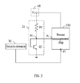
- FIG. 2 shows that the power supply 10 includes a power source V1.
- the detection unit 21 includes a transistor Q1 and a first resistor R1.
- a base of the transistor Q1 is connected to the power source V1 through the resistor R1.
- An emitter of the transistor Q1 is grounded.
- a collector of the transistor Q1 is connected to the base of the transistor Q1.
- a turned-on voltage of the transistor Q1 is variably changed by the temperature. When the voltage difference between the base and the emitter exceeds the turned-on voltage, the transistor Q1 turns on.
- the transistor Q1 is an npn type bipolar junction transistor.
- the control unit 23 includes a power management chip 230.
- the power management chip 230 includes an adjusting pin P1 and an output pin P2.
- the adjusting pin P1 is connected to the base of the transistor Q1.
- the output pin P2 is connected to the switching element 30.
- a working method of the electronic device 100 is described as follows.
- the power supply 10 outputs the working voltage
- the voltage difference between the base and the emitter of the transistor Q1 is more than the turned-on voltage
- the transistor Q1 turns on.
- the voltage of the detecting pin P1 is equal to the turned-on voltage of the transistor Q1.
- the power management chip 230 outputs the PWM signal based on the voltage of the detecting pin P1 to control the power of the switching element 30.
- the switching element 30 operates and generates heat.
- the heat generated by the switching element 30 is increased, the turned-on voltage of the transistor Q1 decreases.
- the voltage of the detecting pin P1 is decreased, the power management chip 230 decreases the power of the PWM signal to decrease the heat generated by the switching element 30.
- the power of the switching element 30 is automatically adjusted based on the heat generated by the switching element 30, such that the temperature of the electronic device 100 is being controlled, and the performance of the electronic device 100 is improved.
Landscapes
- Engineering & Computer Science (AREA)
- Power Engineering (AREA)
- Dc-Dc Converters (AREA)
- Electronic Switches (AREA)
Abstract
Description
- The present disclosure relates to an electronic device with an adjustment circuit.
- Some electronic devices include at least one high power switching element. When the switching element operates, heat is generated and this increases the temperature inside of the electronic device. However, as the temperature increases, other elements in the electronic device may decrease in performance or even malfunction.
- Therefore, there is room for improvement in the art.
- According to an exemplary embodiment of the invention, an electronic device detects the heat generated by a switching element for adjusting the power of the switching element by an adjustment circuit. The adjustment circuit includes a detection unit and a control unit which are parallel connected between the power supply and the switching element. The control unit generates PWM signal to drive the switching element. The detection unit detects the heat generated by the switching element and outputs a detected voltage to control the control unit to adjust the duty cycle of the PWM signal in real time.
- Many aspects of the embodiments can be better understood with reference to the following drawings. The components in the drawings are not necessarily drawn to scale, the emphasis instead being placed upon clearly illustrating the principles of the embodiments. Moreover, in the drawings, like reference numerals designate corresponding parts throughout two views.
-
FIG. 1 is a block diagram of an embodiment of an electronic device. -
FIG. 2 is a circuit diagram of an embodiment of the electronic device ofFIG. 1 . -
FIG. 1 shows an embodiment of anelectronic device 100. Theelectronic device 100 includes at least one highpower switching element 30. Theelectronic device 100 detects a heat generated by the operatedswitching element 30 to automatically adjust the power of theswitching element 30 to prevent a temperature inside of theelectronic device 100 from being too high. In one embodiment, theelectronic device 100 can be a computer, an air conditioner, or a television. - The
electronic device 100 further includes apower supply 10 and anadjustment circuit 20. - The
power supply 10 provides a working voltage to theadjustment circuit 20. In the embodiment, the working voltage is 5 volt (V). - The
adjustment circuit 20 connects between thepower supply 10 and theswitching element 30. Theadjustment circuit 20 generates a pulse width modulation (PWM) signal to drive theswitching element 30. Theadjustment circuit 20 further detects the heat generated by theswitching element 30 to adjust the duty cycle of the PWM signal. Theadjustment circuit 20 includes adetection unit 21 and acontrol unit 23. - The
detection unit 21 detects the heat generated by theswitching element 30 and outputs a detected voltage to thecontrol unit 23. The detected voltage is changed in a linear manner. In one embodiment, for each one degree of the temperature increase, the detected voltage detected by thedetection unit 21 decreases 2-2.5 millivolt (mV). - The
control unit 23 generates a variable duty cycle of the PWM signal to drive theswitching element 30 based on the detected voltage. The PWM signal includes a logic-low signal and a logic-high signal. In one duty cycle, the logic-low signal lasts for a first duration, and the logic-high signal lasts for a second duration. The ratio between the first duration and the second duration is constant in each variable duty cycles of the PWM signal. - The
switching element 30 operates based on the PWM signal and the heat generated by theswitch element 30 can be controlled. -
FIG. 2 shows that thepower supply 10 includes a power source V1. - The
detection unit 21 includes a transistor Q1 and a first resistor R1. A base of the transistor Q1 is connected to the power source V1 through the resistor R1. An emitter of the transistor Q1 is grounded. A collector of the transistor Q1 is connected to the base of the transistor Q1. A turned-on voltage of the transistor Q1 is variably changed by the temperature. When the voltage difference between the base and the emitter exceeds the turned-on voltage, the transistor Q1 turns on. In one embodiment, the transistor Q1 is an npn type bipolar junction transistor. - The
control unit 23 includes apower management chip 230. Thepower management chip 230 includes an adjusting pin P1 and an output pin P2. The adjusting pin P1 is connected to the base of the transistor Q1. The output pin P2 is connected to theswitching element 30. - A working method of the
electronic device 100 is described as follows. When thepower supply 10 outputs the working voltage, the voltage difference between the base and the emitter of the transistor Q1 is more than the turned-on voltage, the transistor Q1 turns on. The voltage of the detecting pin P1 is equal to the turned-on voltage of the transistor Q1. Thepower management chip 230 outputs the PWM signal based on the voltage of the detecting pin P1 to control the power of theswitching element 30. Theswitching element 30 operates and generates heat. When the heat generated by theswitching element 30 is increased, the turned-on voltage of the transistor Q1 decreases. The voltage of the detecting pin P1 is decreased, thepower management chip 230 decreases the power of the PWM signal to decrease the heat generated by theswitching element 30. - In use, the power of the
switching element 30 is automatically adjusted based on the heat generated by theswitching element 30, such that the temperature of theelectronic device 100 is being controlled, and the performance of theelectronic device 100 is improved. - It is to be understood, however, that even though information and advantages of the present embodiments have been set forth in the foregoing description, together with details of the structures and functions of the present embodiments, the disclosure is illustrative only; and changes may be made in detail, especially in the matters of shape, size, and arrangement of parts within the principles of the present embodiments to the full extent indicated by the broad general meaning of the terms in which the appended claims are expressed.
Claims (12)
- An electronic device, comprising:a power supply for providing a working voltage;a switching element capable of generating heat when operating;an adjustment circuit connected between the power supply and the switching element, capable of generating a pulse width modulation (PWM) signal to drive the switching element to work;wherein the adjustment circuit powered by the working voltage comprises a detection unit and a control unit which are connected between the power supply and the switching element; the detection unit detects the heat generated by the switching element and outputs a detected voltage; the control unit adjusts the duty cycle of the PWM signal based on the detected voltage.
- The electronic device of claim 1, wherein the PWM signal includes a logic-low signal and a logic-high signal; the logic-low signal lasts for a first duration in one duty cycle, and the logic-high signal lasts for a second duration in one duty cycle; the ratio between the first duration and the second duration is constant in different duty cycles.
- The electronic device of claim 1 or 2, wherein for each one degree of the temperature increase, the detected voltage detected by the detection unit decreases 2-2.5 millivolt (mV).
- The electronic device of claim 1, 2, or 3, wherein the detected voltage is changed in a linear manner.
- The electronic device of claim 1, 2, 3, or 4, wherein the detection unit includes a transistor and a first resistor; a base of the transistor is connected to the power supply through the resistor; an emitter of the transistor is grounded; a collector of the transistor is connected to the base of the transistor, a turned-on voltage of the transistor is variable changed by the fluctuation in temperature.
- The electronic device of claim 5, wherein the transistor is an npn type bipolar junction transistor.
- An adjustment circuit connected between a power supply and a switching element which generates heat when operates; the power supply generating a working voltage; the adjustment circuit comprising:a detection unit powered by the working voltage; anda control unit powered by the working voltage, for generating a pulse width modulation (PWM) signal to drive the switching element to work;wherein the detection unit and the control unit are connected between the power supply and the switching element; the detection unit detects the heat generated by the switching element and outputs a detected voltage; the control unit adjusts the duty cycle of the PWM signal based on the detected voltage.
- The electronic device of claim 7, wherein the PWM signal includes a logic-low signal and a logic-high signal; the logic-low signal lasts for a first duration in one duty cycle, and the logic-high signal lasts for a second duration in one duty cycle; the ratio between the first duration and the second duration is constant in different duty cycles.
- The electronic device of claim 7 or 8, wherein for each one degree of the temperature increase, the detected voltage detected by the detection unit decreases 2-2.5 millivolt (mV).
- The electronic device of claim 7, 8, or 9, wherein the detected voltage is changed in a linear manner.
- The electronic device of claim 7, 8, 9, or 10, wherein the detection unit includes a transistor and a first resistor; a base of the transistor is connected to the power supply through the resistor; an emitter of the transistor is grounded; a collector of the transistor is connected to the base of the transistor, a turned-on voltage of the transistor is variable changed by the fluctuation in temperature.
- The electronic device of claim 11, wherein the transistor is an npn type bipolar junction transistor.
Applications Claiming Priority (1)
| Application Number | Priority Date | Filing Date | Title |
|---|---|---|---|
| CN201310262186.3A CN104253605A (en) | 2013-06-27 | 2013-06-27 | Adjustment circuit and electronic device with same |
Publications (2)
| Publication Number | Publication Date |
|---|---|
| EP2819287A2 true EP2819287A2 (en) | 2014-12-31 |
| EP2819287A3 EP2819287A3 (en) | 2015-07-22 |
Family
ID=50389190
Family Applications (1)
| Application Number | Title | Priority Date | Filing Date |
|---|---|---|---|
| EP14157976.3A Withdrawn EP2819287A3 (en) | 2013-06-27 | 2014-03-05 | Adjustment circuit and electronic device thereof |
Country Status (4)
| Country | Link |
|---|---|
| US (1) | US20150002120A1 (en) |
| EP (1) | EP2819287A3 (en) |
| CN (1) | CN104253605A (en) |
| TW (1) | TW201500884A (en) |
Families Citing this family (1)
| Publication number | Priority date | Publication date | Assignee | Title |
|---|---|---|---|---|
| CN111782026A (en) * | 2019-04-04 | 2020-10-16 | 鸿富锦精密工业(武汉)有限公司 | Mainboard protection circuit and electronic device with mainboard protection circuit |
Family Cites Families (6)
| Publication number | Priority date | Publication date | Assignee | Title |
|---|---|---|---|---|
| JP5161641B2 (en) * | 2008-04-18 | 2013-03-13 | 株式会社東芝 | Temperature detection circuit |
| KR101656774B1 (en) * | 2009-12-16 | 2016-09-12 | 삼성전자주식회사 | Method and Apparatus for controlling temperature of the fusing system in image forming apparatus, and image forming apparatus having it |
| JP2012048552A (en) * | 2010-08-27 | 2012-03-08 | On Semiconductor Trading Ltd | Control circuit of switching device |
| US20130187619A1 (en) * | 2012-01-19 | 2013-07-25 | Fairchild Semiconductor Corporation | Shunt regulator |
| US9506817B2 (en) * | 2012-05-12 | 2016-11-29 | Integrated Device Technology, Inc | Temperature detection method and device with improved accuracy and conversion time |
| JP5408316B1 (en) * | 2012-09-11 | 2014-02-05 | オムロン株式会社 | Electromagnetic relay control unit and electromagnetic relay control method |
-
2013
- 2013-06-27 CN CN201310262186.3A patent/CN104253605A/en active Pending
- 2013-07-04 TW TW102123958A patent/TW201500884A/en unknown
-
2014
- 2014-01-06 US US14/147,622 patent/US20150002120A1/en not_active Abandoned
- 2014-03-05 EP EP14157976.3A patent/EP2819287A3/en not_active Withdrawn
Non-Patent Citations (1)
| Title |
|---|
| None |
Also Published As
| Publication number | Publication date |
|---|---|
| US20150002120A1 (en) | 2015-01-01 |
| EP2819287A3 (en) | 2015-07-22 |
| CN104253605A (en) | 2014-12-31 |
| TW201500884A (en) | 2015-01-01 |
Similar Documents
| Publication | Publication Date | Title |
|---|---|---|
| US8410405B2 (en) | Temperature control system | |
| US7702223B2 (en) | Circuit for controlling rotation speed of computer fan | |
| US20140147289A1 (en) | Fan control circuit | |
| US9176200B2 (en) | Power supply test device | |
| US9229033B2 (en) | Voltage detecting system | |
| US8248016B2 (en) | Fan circuit | |
| TW201422917A (en) | Fan control circuit of computer | |
| US20120068652A1 (en) | Fan drive circuit for electronic device | |
| US11523481B2 (en) | Combinational circuit and control circuit | |
| US20130147632A1 (en) | Indicator light control circuit | |
| US8896253B2 (en) | Control circuit for fan | |
| US9488183B2 (en) | Fan rotation speed controlling device | |
| US20120098438A1 (en) | Illumination adjustment circuit | |
| US9109604B2 (en) | Fan control circuit | |
| TW201534022A (en) | Electronic device power supply system | |
| US20150002120A1 (en) | Adjustment circuit and electronic device thereof | |
| US20130265718A1 (en) | Heat dissipation circuit and electronic device having the same | |
| CN102734200A (en) | Temperature Control and Speed Regulation System of DC Fan | |
| US9593689B2 (en) | Fan control circuit | |
| US9901006B2 (en) | Control circuit for fan | |
| CN202673736U (en) | A temperature control and speed regulation system for a DC fan | |
| US9695833B2 (en) | Rotational speed control system for fan | |
| US20160265544A1 (en) | Adjustable fan speed | |
| CN119107895B (en) | Drive current regulation circuit, gate driver chip and electronic equipment | |
| US20130175951A1 (en) | Control circuit for light emitting diode of display |
Legal Events
| Date | Code | Title | Description |
|---|---|---|---|
| PUAI | Public reference made under article 153(3) epc to a published international application that has entered the european phase |
Free format text: ORIGINAL CODE: 0009012 |
|
| 17P | Request for examination filed |
Effective date: 20140305 |
|
| AK | Designated contracting states |
Kind code of ref document: A2 Designated state(s): AL AT BE BG CH CY CZ DE DK EE ES FI FR GB GR HR HU IE IS IT LI LT LU LV MC MK MT NL NO PL PT RO RS SE SI SK SM TR |
|
| AX | Request for extension of the european patent |
Extension state: BA ME |
|
| PUAL | Search report despatched |
Free format text: ORIGINAL CODE: 0009013 |
|
| AK | Designated contracting states |
Kind code of ref document: A3 Designated state(s): AL AT BE BG CH CY CZ DE DK EE ES FI FR GB GR HR HU IE IS IT LI LT LU LV MC MK MT NL NO PL PT RO RS SE SI SK SM TR |
|
| AX | Request for extension of the european patent |
Extension state: BA ME |
|
| RIC1 | Information provided on ipc code assigned before grant |
Ipc: H02M 1/32 20070101AFI20150612BHEP Ipc: G01K 7/01 20060101ALI20150612BHEP |
|
| STAA | Information on the status of an ep patent application or granted ep patent |
Free format text: STATUS: THE APPLICATION IS DEEMED TO BE WITHDRAWN |
|
| 18D | Application deemed to be withdrawn |
Effective date: 20160123 |