EP2815587B1 - Physical layer management (plm) in an optical distribution frame - Google Patents
Physical layer management (plm) in an optical distribution frame Download PDFInfo
- Publication number
- EP2815587B1 EP2815587B1 EP13708082.6A EP13708082A EP2815587B1 EP 2815587 B1 EP2815587 B1 EP 2815587B1 EP 13708082 A EP13708082 A EP 13708082A EP 2815587 B1 EP2815587 B1 EP 2815587B1
- Authority
- EP
- European Patent Office
- Prior art keywords
- tray
- connections
- rfid
- positions
- circuit board
- Prior art date
- Legal status (The legal status is an assumption and is not a legal conclusion. Google has not performed a legal analysis and makes no representation as to the accuracy of the status listed.)
- Active
Links
Images


Classifications
-
- G—PHYSICS
- G06—COMPUTING OR CALCULATING; COUNTING
- G06Q—INFORMATION AND COMMUNICATION TECHNOLOGY [ICT] SPECIALLY ADAPTED FOR ADMINISTRATIVE, COMMERCIAL, FINANCIAL, MANAGERIAL OR SUPERVISORY PURPOSES; SYSTEMS OR METHODS SPECIALLY ADAPTED FOR ADMINISTRATIVE, COMMERCIAL, FINANCIAL, MANAGERIAL OR SUPERVISORY PURPOSES, NOT OTHERWISE PROVIDED FOR
- G06Q10/00—Administration; Management
- G06Q10/08—Logistics, e.g. warehousing, loading or distribution; Inventory or stock management
- G06Q10/087—Inventory or stock management, e.g. order filling, procurement or balancing against orders
-
- G—PHYSICS
- G02—OPTICS
- G02B—OPTICAL ELEMENTS, SYSTEMS OR APPARATUS
- G02B6/00—Light guides; Structural details of arrangements comprising light guides and other optical elements, e.g. couplings
- G02B6/44—Mechanical structures for providing tensile strength and external protection for fibres, e.g. optical transmission cables
- G02B6/4439—Auxiliary devices
- G02B6/444—Systems or boxes with surplus lengths
- G02B6/4452—Distribution frames
- G02B6/44524—Distribution frames with frame parts or auxiliary devices mounted on the frame and collectively not covering a whole width of the frame or rack
-
- G—PHYSICS
- G02—OPTICS
- G02B—OPTICAL ELEMENTS, SYSTEMS OR APPARATUS
- G02B6/00—Light guides; Structural details of arrangements comprising light guides and other optical elements, e.g. couplings
- G02B6/44—Mechanical structures for providing tensile strength and external protection for fibres, e.g. optical transmission cables
- G02B6/4439—Auxiliary devices
- G02B6/444—Systems or boxes with surplus lengths
- G02B6/44528—Patch-cords; Connector arrangements in the system or in the box
-
- G—PHYSICS
- G02—OPTICS
- G02B—OPTICAL ELEMENTS, SYSTEMS OR APPARATUS
- G02B6/00—Light guides; Structural details of arrangements comprising light guides and other optical elements, e.g. couplings
- G02B6/44—Mechanical structures for providing tensile strength and external protection for fibres, e.g. optical transmission cables
- G02B6/4439—Auxiliary devices
- G02B6/444—Systems or boxes with surplus lengths
- G02B6/4453—Cassettes
-
- H—ELECTRICITY
- H04—ELECTRIC COMMUNICATION TECHNIQUE
- H04Q—SELECTING
- H04Q1/00—Details of selecting apparatus or arrangements
- H04Q1/02—Constructional details
- H04Q1/13—Patch panels for monitoring, interconnecting or testing circuits, e.g. patch bay, patch field or jack field; Patching modules
- H04Q1/135—Patch panels for monitoring, interconnecting or testing circuits, e.g. patch bay, patch field or jack field; Patching modules characterized by patch cord details
- H04Q1/136—Patch panels for monitoring, interconnecting or testing circuits, e.g. patch bay, patch field or jack field; Patching modules characterized by patch cord details having patch field management or physical layer management arrangements
- H04Q1/138—Patch panels for monitoring, interconnecting or testing circuits, e.g. patch bay, patch field or jack field; Patching modules characterized by patch cord details having patch field management or physical layer management arrangements using RFID
-
- H—ELECTRICITY
- H04—ELECTRIC COMMUNICATION TECHNIQUE
- H04Q—SELECTING
- H04Q1/00—Details of selecting apparatus or arrangements
- H04Q1/02—Constructional details
- H04Q1/15—Backplane arrangements
- H04Q1/155—Backplane arrangements characterised by connection features
-
- H—ELECTRICITY
- H05—ELECTRIC TECHNIQUES NOT OTHERWISE PROVIDED FOR
- H05K—PRINTED CIRCUITS; CASINGS OR CONSTRUCTIONAL DETAILS OF ELECTRIC APPARATUS; MANUFACTURE OF ASSEMBLAGES OF ELECTRICAL COMPONENTS
- H05K5/00—Casings, cabinets or drawers for electric apparatus
- H05K5/02—Details
- H05K5/0256—Details of interchangeable modules or receptacles therefor, e.g. cartridge mechanisms
- H05K5/0286—Receptacles therefor, e.g. card slots, module sockets, card groundings
-
- H—ELECTRICITY
- H05—ELECTRIC TECHNIQUES NOT OTHERWISE PROVIDED FOR
- H05K—PRINTED CIRCUITS; CASINGS OR CONSTRUCTIONAL DETAILS OF ELECTRIC APPARATUS; MANUFACTURE OF ASSEMBLAGES OF ELECTRICAL COMPONENTS
- H05K7/00—Constructional details common to different types of electric apparatus
- H05K7/14—Mounting supporting structure in casing or on frame or rack
- H05K7/1485—Servers; Data center rooms, e.g. 19-inch computer racks
- H05K7/1488—Cabinets therefor, e.g. chassis or racks or mechanical interfaces between blades and support structures
- H05K7/1491—Cabinets therefor, e.g. chassis or racks or mechanical interfaces between blades and support structures having cable management arrangements
-
- G—PHYSICS
- G02—OPTICS
- G02B—OPTICAL ELEMENTS, SYSTEMS OR APPARATUS
- G02B6/00—Light guides; Structural details of arrangements comprising light guides and other optical elements, e.g. couplings
- G02B6/44—Mechanical structures for providing tensile strength and external protection for fibres, e.g. optical transmission cables
- G02B6/4439—Auxiliary devices
- G02B6/444—Systems or boxes with surplus lengths
- G02B6/4453—Cassettes
- G02B6/4455—Cassettes characterised by the way of extraction or insertion of the cassette in the distribution frame, e.g. pivoting, sliding, rotating or gliding
-
- Y—GENERAL TAGGING OF NEW TECHNOLOGICAL DEVELOPMENTS; GENERAL TAGGING OF CROSS-SECTIONAL TECHNOLOGIES SPANNING OVER SEVERAL SECTIONS OF THE IPC; TECHNICAL SUBJECTS COVERED BY FORMER USPC CROSS-REFERENCE ART COLLECTIONS [XRACs] AND DIGESTS
- Y10—TECHNICAL SUBJECTS COVERED BY FORMER USPC
- Y10T—TECHNICAL SUBJECTS COVERED BY FORMER US CLASSIFICATION
- Y10T29/00—Metal working
- Y10T29/49—Method of mechanical manufacture
- Y10T29/49002—Electrical device making
- Y10T29/49004—Electrical device making including measuring or testing of device or component part
Definitions
- This application relates to providing physical layer management in an optical distribution frame.
- One embodiment is directed to a tray for use in a subrack of a rack.
- the tray comprises a printed circuit board configured so that a plurality of connections can be made at a plurality of positions on the printed circuit board, each of the plurality of connections involving at least one connector positioned on a patch side of the plurality of positions and the least one connector having a device associated therewith in which information is stored.
- the tray is configured so that either side of the positions can be used as the patch side.
- the tray is configured so that the devices associated with the connectors involved in making the connections at the patch side can be read via the tray.
- the devices associated with the connections can be implemented, for example, using RFID tags or connection point identifier (CPID) storage devices (such as EEPROMs).
- CPID connection point identifier
- the tray comprises a printed circuit board configured so that a plurality of connections can be made at a plurality of positions on the printed circuit board, each of the positions having at least two sides.
- the method comprises selecting one of the sides as a patch side and making the plurality of connections using the tray.
- Each of the plurality of connections involves at least one connector having a device associated therewith in which information is stored.
- the selected patch side is used as the patch side for each of the plurality of connections.
- the method further comprises reading, via the tray, information stored in the devices associated with the connectors involved in making the connections.
- the devices associated with the connections can be implemented, for example, using RFID tags or connection point identifier (CPID) storage devices (such as EEPROMs).
- CPID connection point identifier
- Another embodiment is directed to a subrack comprising a backplate and at least one tray configured so that a plurality of connections can be made at a plurality of positions on the tray.
- Each of the plurality of connections involves at least one connector having information stored in a device associated therewith that can be read.
- the backplate and the tray are configured so that the tray can be selectively attached and removed from the backplate.
- the backplate and the tray are configured so that the devices associated with the connectors involved in making the connections can be read via the tray.
- the devices associated with the connections can be implemented, for example, using RFID tags or connection point identifier (CPID) storage devices (such as EEPROMs).
- CPID connection point identifier
- Another embodiment is directed to a method of using a subrack that comprises a backplate and at least one tray configured so that a plurality of connections can be made at a plurality of positions on the tray.
- Each of the plurality of connections involves at least one connector having information stored in a device associated therewith.
- the method comprises attaching the tray to the backplate; reading, via the tray, the devices associated with the connectors involved in making the connections; and removing the tray from the backplate and thereafter re-attaching the tray to the backplate.
- the devices associated with the connections can be implemented, for example, using RFID tags or connection point identifier (CPID) storage devices (such as EEPROMs).
- CPID connection point identifier
- a further embodiment is directed to a tray for use in a subrack of a rack, the tray comprising a printed circuit board configured so that a plurality of connections can be made at a plurality of positions on the printed circuit board. Each of the plurality of connections involves at least one connector having an RFID tag associated therewith.
- the tray further comprises a plurality of RFID antennas integrated into the printed circuit board, each the RFID antennas associated with a respective one of the positions.
- the printed circuit board is configured to localize a field emitted from each RFID antenna so that only the RFID tag associated with that RFID antenna is energized and read.
- the tray comprises a printed circuit board and a plurality of RFID antennas integrated into the printed circuit board. Each the RFID antennas associated with a respective one of a plurality of positions on the printed circuit board.
- the method comprises making a plurality of connections at the plurality of positions on the printed circuit board. Each of the plurality of connections involves at least one connector having an RFID tag associated therewith.
- the method further comprises energizing and reading the RFID tags using the RFID antennas and localizing a field emitted from each RFID antenna so that only the RFID tag associated with that RFID antenna is energized and read.
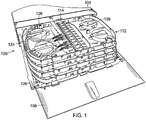
- FIG. 1 illustrates one exemplary embodiment of a subrack 100 (also referred to as a general patch splice patch tray or "GPST").
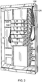
- an optical distribution frame comprises one or more racks in which one or more subracks 100 are mounted.
- a frame 102 in which multiple subracks are mounted is shown in FIG. 2 .
- Each subrack 100 comprises an enclosure 104 and a shelf 106.
- Each subrack 100 is configured so that the shelf 106 can slide in and out of an opening formed in the front of the enclosure 104.
- a front panel 108 is attached to the front of the shelf 106 so that when the shelf 106 has been completely pushed into the enclosure 104, the front panel 108 can be flipped up to close the front opening of the enclosure 104. Also, the front panel 108 can be flipped done to allow the shelf 106 to slide out of the enclosure 104.
- Each subrack 100 includes a backplate 110 that extends generally vertically from the top of the shelf 106.
- Each subrack 100 includes multiple trays 112 that are vertically stacked.
- Each tray 112 is rotatably mounted to the backplate 110 so that the tray 112 can flipped up in order to provide access to the tray 112 that is underneath it (if there is one).
- each tray 112 is removably mounted to the backplate 110 so that the tray 112 can be easily removed from the subrack 100 in order to assist in providing access to that tray or to trays 112 that are underneath it.
- the tray 112 can also be easily re-mounted to the backplate 110.
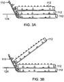
- the backplate 110 is vertically disposed at angle so that the trays 112 are arranged in a stair step configuration (though this need not be the case).
- each tray 112 incorporates managed connectivity technology.
- a plurality of connections can be made at a plurality of positions on the tray 112, where each of the plurality of connections involves at least one connector.
- the managed connectivity technology generally takes the form of a device (for example, an RFID tag or an EEPROM) that is attached to or integrated into at least one connector used to make each such connection. Information is stored in the managed connectivity connector device.
- the tray 112 is configured so that either side of the tray can be used as the patch side of the tray 112. Also, the tray 112 is configured to read the information stored in the managed connectivity devices.
- each tray 112 is configured to hold multiple fiber optic adapters 114 (where each adapter 114 is associated with one of the plurality of positions where a connection can be made).
- Each adapter 114 is configured to optically couple each optical fiber in a set of one or more optical fibers to a respective optical fiber in another set of one or more optical fibers.
- each such set of one or more optical fibers is terminated with a connector 116.
- each such adapter 114 is used to couple a single fiber to another single fiber.
- Each adapter 114 comprises two ports 118 to receive and hold the two connectors 116 in place while optically coupling the fibers.
- fiber optic adapters 114 and connectors 116 examples include SC, LC, FC, LX.5, MTP, or MPO connectors. Other adapters and connectors can used.
- the fiber optic adapters 114 are arranged and held on the tray 112 so that the ports 118 on each side of the adapters 114 all face the same direction and are aligned with one another.
- each tray 112 and the adapters 114 held by that tray 112 are described as having a first or left side and a second or right side.
- each adapter 114 is held on the tray 112 by a plastic clip 120. This allows each fiber optic adapter 114 to be easily removed and attached to the tray 112.
- each tray 112 can be configured to have one side of the tray 112 and adapters 114 serve as the "patch field" or "patch side".
- the patch side is the side of the tray and adapters where the optical patching is performed.
- the other side of the tray 112 and adapters 114 serve as the "fixed side”.
- connectors 116 attached to one end of optical patch cords 122 are attached to the ports 118 on the patch side.
- Connectors attached to the other end of the patch cords exit that tray and are typically connected to a port on the patch side of another adapter or another device in the network.
- the fixed optical cabling 124 can be an optical pigtail, in which case the other end of the pigtail comprises a fiber that is spliced (for example, using a smooth) to another longer optical fiber that exits the tray 112.
- the other end of the longer cable is connected as appropriate (for example, at another optical node located somewhere else in the network).
- the fixed optical cables 124 that are connected to the ports 118 on the fixed side of the tray 112 can themselves exit the tray 112 (like the patch cords 122 attached to the ports 118 on the patch side of the tray 112) and can be connected as appropriate (for example, at another optical node located somewhere else in the network).
- each tray 112 typically is configured to include two removable island assemblies 126, where one island assembly 126 is attached to the patch side of the tray 112 and the other island assembly 126 is attached to the fixed side of the tray 112.
- the island assemblies 126 are configured to facilitate the routing and/or splicing of the fiber optic cabling that is attached to the ports 118 on that side.
- the island assemblies 126 in each tray can be reconfigured as needed by removing and inserting appropriate island assemblies 126.
- the connectors 116 attached to the patch side of the adapters 114 have RFID tags 128 (shown in FIG. 4 ) attached, or integrated into, them.
- the RFID tags 128 store a unique identifier for the connector 116 and/or the patch cord 122 that can be used to identify which patch cord 122 is attached to each patch port 118.
- the RFID tags 128 can store other information, and can be written to as well as read from.
- a printed circuit board 130 (also referred to here as the "tray PCB" 130) is attached to the bottom of each tray 112.
- the tray PCB 130 includes a respective RFID antenna or coil 132 and respective LED (or other visual indicator) 134 positioned near each side of each fiber optic adapter 114. That is, each fiber optic adapter 114 has a associated pair of RFID antennas 132, a first one of which is located near a first one port 118 of the adapter 114 and second one of which is located near the other port 118 of the adapter 114.
- Each RFID antenna or coil 132 is used for reading an RFID tag 130 inserted into the respective port 118, and each LED or other visual indicator 134 is used for visually identifying the respective port 118 (for example, in connection with guiding a technician in carrying out a work order).
- the ports 118 on only one side of the tray 112 are used as the patch ports at any given time, there are RFID antennas or coils 132 and LEDs (or other visual indicators) 134 positioned on each side of the adapters 114 so that the same tray 112 and tray PCB 130 can be used to support patching on either side of the tray 112.
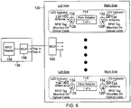
- a PCB 136 is mounted in the shelf 106 of each subrack 100.
- This PCB 136 is also referred to here as the "subrack PCB” 136 or the “subrack controller card” 136.
- Components of the subrack PCB 136 are coupled to components on each of the tray PCBs 130 using a backplane PCB 138.
- the subrack PCB 136 includes a flexible circuit or ribbon cable 140 to which a suitable backplane connector 142 is attached. This backplane connector 142 is attached to a connector on the backplane PCB 144.
- each tray PCB 130 includes a flexible circuit or ribbon cable 144 to which a suitable backplane connector 146 is attached.
- This backplane connector 146 is attached to a connector 148 on the backplane PCB 138.
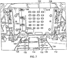
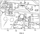
- the backplane connector 148 of each tray 112 is held in place by a pair of tethers 150 (for example, plastic tethers typically used for attaching price tags to items of clothing and the like) that are attached to both the tray 112 and the backplane connector 146. See FIGS. 7-11 .
- the tethers 150 and backplane connector 146 are configured so that when the tray 118 is removed from the backplate 110 (backplane PCB 138), the tethers 150 will pull the backplane connector 146 out of the connector 148 on the backplane 138 before the flexible circuit or ribbon cable 144 is pulled on. This is done to protect the flexible circuit or ribbon cable 144 from being damaged by removing the tray 112 from the backplane 138. Also, the tethers 150 help hold the backplane connector 146 in place to ease insertion of the backplane connector 146 onto the connector 148 on the backplane PCB 138 when the tray 112 is re-attached.
- the backplate 110 to which the trays 112 are attached comprises the backplane PCB 138. That is, the functions of the backplate 110 are performed at least in part by the backplane PCB 138. Moreover, the backplane PCB 138 includes cut outs 152 to which plastic strain relief cables 154 can be attached. Strain relief cables 154 are used to hold the fiber optic cabling attached to the ports 118 of that tray 112 in place so as to relieve the strain (for example, due to pulling on the cables) that otherwise might affect the cables or the connections provided at the ports 118 or splices housed in the tray 112.
- the subrack PCB 136 includes an RFID reader 156.
- the RFID reader 156 can be selectively coupled to the pair of RFID antennas or coils 132 positioned near each of the adapters 114 in each subrack 100.
- the subrack PCB 136 includes a first multiplexer 158 to couple the RF I/O port of the RFID reader 156 to another multiplexer 160 located on one of the tray PCBs 130.
- a multiplexer 160 located on each tray PCB 130 is used to selectively couple the RF I/O port of the RFID reader 156 to one of the RFID antenna pairs 132 included on that tray PCB 130.
- a controller 162 is located on the subrack PCB 136, and a controller 164 is located on each of the tray PCBs 130.
- Each controller 162 and 164 can be implemented using a suitable programmable processor for executing software.
- the software executing on the programmable processor performs at least some of the processing described here as being performed by each of the controllers 162 and 164.
- the subrack controller 162 is coupled to the RFID reader 156, the subrack multiplexer 158, and an LED 166 that is mounted to the subrack 100 (for example, to the front panel 108 of the subrack 100). Also, the subrack controller 162 is coupled to each of the tray controllers 164 via the backplane 138.
- Each tray controller 164 is coupled to the tray multiplexer 160 on that tray 112 and the LEDs (or other visual indicators) 134 on that tray 112.
- the subrack controller 162 is coupled to an overall rack controller 168 (also referred to here as the "analyzer").
- the analyzer 168 is configured to cause the subrack controller 162 and the tray controllers 164 to read the RFID tag 128 that is attached to any connector 116 inserted into each patch port 118. This can be done in a polling manner, where periodically each such patch port 118 is read. This can be done in other ways as well. Reading of a particular RFID tag 128 is done by instructing the subrack controller 162 and tray controller 164 to configure the multiplexers 158 and 160 to couple the RFID reader 156 to the appropriate RFID antennas or coils 132.
- the RFID antennas 132 and LEDs 134 on both sides of the adapter 114 are coupled to the tray controller 164 and to power and ground using the same PCB traces.
- a first set of PCB traces for coupling the RFID antennas 132 and LEDs 134 on the left side of each adapter 114 and a second, separate set of PCB for coupling the RFID antennas 132 and LEDs 134 on the right side of that adapter 114 need not be provided; instead, for each adapter 114, only a single set of PCB traces need be provided for coupling the RFID antennas 132 and LEDs 134 on both sides of each adapter 114 to the tray controller 164 and power and ground.
- the analyzer 168 is also configured to communicate the information read from the RFID tags 128 to middleware software 170 in the manner described in the following US Patent Applications: United States Provisional Patent Application Serial No. 61/152,624, filed on February 13, 2009 , titled “MANAGED CONNECTIVITY SYSTEMS AND METHODS" (also referred to here as the "'624 Application”); United States Patent Application Serial No. 12/705,497, filed on February 12, 2010 , titled “AGGREGATION OF PHYSICAL LAYER INFORMATION RELATED TO A NETWORK” (is also referred to here as the '497 Application); United States Patent Application Serial No.
- the middleware software 170 includes, or is coupled to a database or other data store (not shown) for storing the information provided to it.
- the middleware software 170 also includes functionality that provides an interface for external devices or entities to access the information maintained by the middleware software 170. This access can include retrieving information from the middleware software 170 as well as supplying information to the middleware software 170.
- the middleware software 170 is implemented as "middleware" that is able to provide such external devices and entities with transparent and convenient access to the information maintained by the middleware software 170.
- the middleware software 170 aggregates information from the relevant devices in the network and provides external devices and entities with access to such information, the external devices and entities do not need to individually interact with all of the devices in the network that provide such information, nor do such devices need to have the capacity to respond to requests from such external devices and entities.
- the middleware software 170 implements an application programming interface (API) by which application-layer functionality can gain access to the physical layer information maintained by the middleware software 170 using a software development kit (SDK) that describes and documents the API.
- API application programming interface
- SDK software development kit
- ICM Infrastructure Configuration Manager
- the analyzer 168 is also configured to instruct the subrack controller 162 and/or the tray controllers 164 to turn on the LEDs (or other visual indicators) 134 as appropriate (for example, in connection with instructing a technician in carrying out a work order or to signal an error condition).
- the analyzer 168 can be configured to guide a technician in carrying out a work order by visually signally which ports 118 are to be affected by a particular step in the work order using the LEDs 134.
- the LEDs 134 can be used to provide a visual indication as to whether each step was properly carried out. Data read from the RFID tags 18 is also used to determine if each step was properly carried out (for example, in similar manner as is described in the previously mentioned US patent applications).
- data can be written to the RFID tags 128 in the same manner.
- these two connectors 174 can be oriented at an angle (for example, 30 degrees to 45 degrees) to facilitate routing this cable 172 in a manner that is compatible with the fiber optic cables in the rack 102. Either of the two connectors 174 can be used depending on what is more convenient for connecting to the analyzer 168. Also, the two connectors 174 can be used to connect multiple subracks 100 to the analyzer 168 using a daisy chain topology.
- the tray 112 can include pockets 176 in the plastic of the tray 112 to accommodate components that are mounted to the underside of the tray PCB board 130. This enables the tray PCB 130 to lay flat in the tray 112.
- the ground planes surround the conductive plane in which the RFID inductors (coil or antenna) are formed. Openings are formed in the upper ground plane in order to enable RF signals to pass between the RFID antenna 134 and any RFID tag 128 positioned above it. The rest of the ground plane serves to constrain the RFID signals. Also, in this example, the openings formed in the bottom of the ground plane serve to let some of the RFID signals escape through the bottom to reduce the size of the field that is created above the tray PCB 130.
- FIG. 14 illustrates another way in which radio frequency fields emitted by RFID antennas can be constrained that is suitable for use in the exemplary subrack of FIG. 1 .
- the layers of the tray PCB 130 are configured so that, for each RFID antenna 132 on each tray 113, the tray PCB 130 includes a multi-layer coil assembly 1404 that implements that RFID antenna 132.
- the layers of the tray PCB 130 are also configured so that, for each RFID antenna 132 on each tray 113, the tray PCB 130 includes a respective C-shaped open copper track feature 1402 and a respective O-shaped closed copper track feature 1404 that concentrically surround the coil assembly 1404.
- the C-shaped open feature 1404 is located inside of the O-shaped closed feature 1406.
- Each respective coil assembly 1402, C-shaped open feature 1404, and O-shaped closed feature 1406 are isolated from each another.
- Each C-shaped open feature 1402 provides a dampening field for producing a rectangular region of interest (ROI) box for addressing misalignment problems that may otherwise occur in general usage.
- Each C-shaped open feature 1042 also provides rear field dampening to the tray 112 below.
- Each O-shaped closed features 1406 provides protection against cross-talk that may otherwise occur among adjacent RFID antennas 132, where each such O-shaped closed feature 1406 is implemented as shorted turn that produces a corresponding nulling field.
- a daughter board 200 it is necessary to position a daughter board 200 onto the tray PCBs 130.
- a storage device such as an EEPROM
- EEPROM electrically erasable programmable read-only memory
- QUAREO QUAREO technology that is commercially available from TE Connectivity. This technology is also referred to here as "Connection Point Identifier" or "CPID" technology.
- the storage device interface comprises four leads -- a power lead, a ground lead, a data lead, and an extra lead that is reserved for future use.
- a suitable protocol for example, the UNI/O protocol
- each adapter 114 that are configured to come into electrical contact with the four corresponding storage-device leads on a connector inserted in that adapter 114.
- Appropriate traces are provided on the tray PCB 130 in the tray 112 to couple these adapter contacts to the tray controller 164 via multiplexer 160 and to power and ground.
- the connectivity between the subrack controller 162 and the tray controllers 164 is provided in the manner described above. In this way, the QUAREO (or similar CPID) technology can be integrated into what is otherwise an RFID subrack 100 to support the mixing and matching of CPID and RFID trays in the field.
- the contacts for reading the storage devices can be attached to a daughter board 200 (shown in FIGS. 12 and 13 ). It is helpful to precisely align this daughter board 200 while attaching it to an appropriate daughter-board connector 202 on the tray PCB 136. One way of doing this is shown in FIGS. 12 and 13 .
- One side of the daughter board 200 has one or more metal pins 204 extending from it.
- the tray PCB 136 includes a corresponding plastic post 206.
- the pins 204 and posts 206 are arranged so that each pin 204 can be inserted into the top of a corresponding one of the posts 206 on the tray PCB 136.
- the connectors 210 and 208 on the daughterboard 200 and tray PCB 136 can more easily be connected while providing more precise alignment of the items on the daughter board 200 (for example, the interfaces for reading the EEPROMS, which in this example are positioned above the fiber optic adapters 114, which are preferably precisely aligned in order to read the EEPROMS).
- the CPID contacts 220 can be placed on both sides of the adapters 114 so that either side of the adapters 114 can be used as the patch field in the manner described above connection with RFID versions of trays.
- CPID contacts 220 on both sides of the adapter 114 are coupled to the tray controller 164 and to power and ground using the same PCB traces.
- a first set of PCB traces for coupling the CPID contacts 220 on the left side of each adapter 114 and a second, separate set of PCB for coupling the CPID contacts 22- on the right side of that adapter 114 need not be provided; instead, for each adapter 114, only a single set of PCB traces need be provided for coupling the CPID contacts 220 on both sides of each adapter 114 to the tray controller 164 and power and ground.
- Example 1 includes a tray for use in a subrack of a rack, the tray comprising: a printed circuit board configured so that a plurality of connections can be made at a plurality of positions on the printed circuit board, each of the plurality of connections involving at least one connector positioned on a patch side of the plurality of positions and the least one connector having a device associated therewith in which information is stored; wherein the tray is configured so that either side of the positions can be used as the patch side; and wherein the tray is configured so that the devices associated with the connectors involved in making the connections at the patch side can be read via the tray.
- Example 2 includes the tray of Example 1, wherein each of the plurality of connections involves at least one connector having an RFID tag associated therewith; and wherein the tray further comprises a plurality of pairs of RFID antennas, each pair of RFID antennas being associated with a respective one of the positions, wherein a respective one of each pair of RFID antennas is associated with each side; wherein the tray is configured so that the RFID antennas associated with the side used as the patch side are used to read the RFID tags associated with the connectors involved in making the connections.
- Example 3 includes the tray of Example 2, wherein each of the plurality of RFID antennas can be selectively coupled to an RFID reader in order to read the RFID tags associated with the connectors involved in making the connections.
- Example 4 includes the tray of Example 1, wherein each of the plurality of connections involves at least one connector having a connection point identifier (CPID) storage device associated therewith, the CPID storage device comprising one or more contacts used for reading the CPID storage device; and wherein the tray further comprises a plurality of pairs of contacts, each pair of contacts being associated with a respective one of the positions; wherein the tray is configured so that contacts of the tray associated with the side used as the patch side are used to read the CPID storage devices associated with the connectors involved in making the connections.
- CPID connection point identifier
- Example 5 includes the tray of any of the Examples 1-4, further comprising a plurality of pairs of visual indicators each pair of visual indicators being associated with a respective one of the positions, wherein a respective one of the pair of visual indicators is associated with a respective side of the positions.
- Example 6 includes the tray of Example 5, wherein at least some of the visual indicators comprise a light emitting diode.
- Example 7 includes the tray of any of the Examples 1-6, wherein the printed circuit board is configured so that a plurality of fiber optic adapters can be attached to the printed circuit board, each of the plurality of fiber optic adapters associated with a respective one of the positions.
- Example 8 includes the tray of Example 7, wherein a plurality of clips is attached to the printed circuit board so that each of the plurality of fiber optic adapters can be removably attached to the printed circuit board.
- Example 9 includes the tray of any of the Examples 1-8, further comprising: a tray controller; at least two communication ports each of which is coupled to the tray controller, wherein the tray is configured so that the tray controller can be coupled to a controller external to the tray via one or more of the communication ports.
- Example 10 includes the tray of Example 9, wherein the communication ports are angled.
- Example 11 includes the tray of any of the Examples 1-10, wherein the each of the plurality of connections is made using at least one of optical cabling and metallic cabling.
- Example 12 includes the tray of any of the Examples 1-11, wherein the tray includes pockets formed in the tray to accommodate components.
- Example 13 includes a method of using a tray, the tray comprising a printed circuit board configured so that a plurality of connections can be made at a plurality of positions on the printed circuit board, each of the positions having at least two sides, wherein the method comprises: selecting one of the sides as a patch side; making the plurality of connections using the tray, each of the plurality of connections involving at least one connector having a device associated therewith in which information is stored and wherein the selected patch side is used as the patch side for each of the plurality of connections; and reading, via the tray, information stored in the devices associated with the connectors involved in making the connections.
- Example 14 includes the method of Example 13, wherein each of the plurality of connections involves at least one connector having an RFID tag associated therewith; and wherein the tray further comprises a plurality of pairs of RFID antennas, each pair of RFID antennas being associated with a respective one of the positions, wherein a respective one of the pair of RFID antennas is associated with a respective side of the positions; and wherein reading, via the tray, information stored in the devices associated with the connectors involved in making the connections comprises: reading the RFID tags associated with the connectors involved in making the connections using the RFID antennas associated with the selected patch side.
- Example 15 includes the method of Example 14, further comprising selectively coupling each of the plurality of RFID antennas to an RFID reader in order to read any RFID tag associated with the connector involved in making the associated connection.
- Example 16 includes the method of Example 13, wherein each of the plurality of connections involves at least one connector having a connection point identifier (CPID) storage device associated therewith, the CPID storage device comprising one or more contacts used for reading the CPID storage device; and wherein the tray further comprises a plurality of pairs of contacts, each pair of contacts being associated with a respective one of the positions; and wherein reading, via the tray, information stored in the devices associated with the connectors involved in making the connections comprises: reading the CPID storage devices associated with the connectors involved in making the connections using the contacts of the tray associated with the selected patch side.
- CPID connection point identifier
- Example 17 includes the method of any of the Examples 13-16, wherein the tray further comprises a plurality of pairs of visual indicators, each pair of visual indicators being associated with a respective one of the positions, wherein a respective one of the pair of visual indicators is associated with a respective side of the positions; and wherein the method further comprises providing visual indications using the visual indicators using the visual indicators associated with the selected patch side.
- Example 18 includes the method of any of the Examples 13-17, wherein the printed circuit board is configured so that a plurality of fiber optic adapters can be attached to the printed circuit board, each of the plurality of fiber optic adapters associated with a respective one of the positions.
- Example 19 includes the method of Example 18, further comprising removably attaching each of the plurality of fiber optic adapters to the tray.
- Example 20 includes a subrack comprising: a backplate; at least one tray configured so that a plurality of connections can be made at a plurality of positions on the tray, each of the plurality of connections involving at least one connector having information stored in a device associated therewith that can be read; wherein the backplate and the tray are configured so that the tray can be selectively attached and removed from the backplate; and wherein the backplate and the tray are configured so that the devices associated with the connectors involved in making the connections can be read via the tray.
- Example 21 includes the subrack of Example 20, wherein the devices associated with each connector comprises RFID tags, wherein the backplate and the tray are configured so that the RFID tags associated with the connectors involved in making the connections can be read via the tray.
- Example 22 includes the subrack of Example 21, wherein each tray comprises a plurality of RFID antennas, each of the RFID antennas being associated with a respective one of the positions, wherein each of the plurality of RFID antennas can be selectively coupled to an RFID reader in order to read the RFID tags associated with the connectors involved in making the connections.
- Example 23 includes the subrack of Example 20, wherein the devices associated each connector comprises connection point identifier (CPID) storage devices, wherein the backplate and the tray are configured so that the CPID storage devices associated with the connectors involved in making the connections can be read via the tray.
- CPID connection point identifier
- Example 24 includes the subrack of any of the Examples 20 to 23, wherein the backplate is implemented as a backplane printed circuit board.
- Example 25 includes the subrack of Example 24, wherein the backplane printed circuit board comprises a tray connector, wherein the tray has attached thereto a backplane connector that is configured to be connected to the tray connector of the backplane printed circuit board in connection with the tray being attached to the backplate; and wherein the tray further comprises at least one plastic tether attached to the backplane connector, wherein the plastic tether is configured to pull the backplane connector out of the tray connector on the backplane printed circuit board in connection with the tray being removed from the backplate.
- Example 26 includes the subrack of any of the Examples 24 or 25, wherein the backplane printed circuit board comprises at least one cut out to which a strain relief cable can be attached.
- Example 27 includes the subrack of any of the Examples 20 to 26, further comprising a plurality of trays.
- Example 28 includes the subrack of any of the Examples 20 to 27 wherein each tray comprises a plurality of visual indicators, each of the visual indicators being associated with a respective one of the positions.
- Example 29 includes the subrack of any of the Examples 20 to 28, wherein each tray is configured so that a plurality of fiber optic adapters can be attached to the printed circuit board, each of the plurality of fiber optic adapters associated with a respective one of the positions.
- Example 30 includes the subrack of any of the Examples 20 to 29, further comprising a subrack controller, wherein each tray comprises: a tray controller; and at least two communication ports, each of which is coupled to the tray controller, wherein the subrack is configured so that the tray controller can be coupled to the subrack controller via one or more of the communication ports.
- Example 31 includes the subrack of Example 30, wherein the communication ports are angled.
- Example 32 includes the subrack of any of the Examples 20 to 31, wherein each tray includes pockets formed in the tray to accommodate electronics.
- Example 33 includes the subrack of any of the Examples 20 to 32, wherein the each of the plurality of connections is made using at least one of optical cabling and metallic cabling.
- Example 34 includes a method of using a subrack that comprises a backplate and at least one tray configured so that a plurality of connections can be made at a plurality of positions on the tray, each of the plurality of connections involving at least one connector having information stored in a device associated therewith, the method comprising: attaching the tray to the backplate; reading, via the tray, the devices associated with the connectors involved in making the connections; and removing the tray from the backplate and thereafter re-attaching the tray to the backplate.
- Example 35 includes the method of Example 34, wherein the devices associated each connector comprises RFID tags; and wherein reading, via the tray, the devices associated with the connectors involved in making the connections comprises reading, via the tray, the RFID tags associated with the connectors involved in making the connections.
- Example 36 includes the method of Example 35, wherein each tray comprises a plurality of RFID antennas, each of the RFID antennas being associated with a respective one of the positions; and wherein reading the RFID tags associated with the connectors involved in making the connections via the tray comprises selectively coupling each of the plurality of RFID antennas to an RFID reader in order to read the RFID tags associated with the connectors involved in making the connections.
- Example 37 includes the method of Example 34, wherein the devices associated each connector comprises connection point identifier (CPID) storage devices; and wherein reading, via the tray, the devices associated with the connectors involved in making the connections comprises reading the CPID storage devices associated with the connectors involved in making the connections via the tray.
- CPID connection point identifier
- Example 38 includes the method of any of the Examples 34 to 37, wherein the backplate is implemented as a backplane printed circuit board.
- Example 39 includes the method of Example 38, wherein the backplane printed circuit board comprises a tray connector, wherein the tray has attached thereto a backplane connector that is configured to be connected to the tray connector of the backplane printed circuit board in connection with the tray being attached to the backplate; and wherein the tray further comprises at least one plastic tether attached to the backplane connector, wherein the plastic tether is configured to pull the backplane connector out of the tray connector on the backplane printed circuit board in connection with the tray being removed from the backplate.
- Example 40 includes the method of any of the Examples 38 to 39, further comprising attaching a strain relief cable to the tray using a cut out formed in the backplane printed circuit board.
- Example 41 includes a tray for use in a subrack of a rack, the tray comprising: a printed circuit board configured so that a plurality of connections can be made at a plurality of positions on the printed circuit board, each of the plurality of connections involving at least one connector having an RFID tag associated therewith; a plurality of RFID antennas integrated into the printed circuit board, each the RFID antennas associated with a respective one of the positions; and wherein the printed circuit board is configured to localize a field emitted from each RFID antenna so that only the RFID tag associated with that RFID antenna is energized and read.
- Example 42 includes the tray of Example 41, wherein the printed circuit board comprises a conductive plane surrounded on an upper side by a first ground plane and surrounded on a bottom side by a second ground plane; and wherein the RFID antennas are formed in the conductive layer of the printed circuit board.
- Example 43 includes the tray Example 42, wherein, for each RFID antenna, a respective opening is formed in the upper ground plane so that radio frequency signals can pass between the respective RFID antenna and any RFID tag positioned near the opening, wherein the rest of the ground plane is configured to constrain the radio frequency signals emitted from the RFID antennas.
- Example 44 includes the tray of Example 43, wherein, for each RFID antenna, a respective opening is formed in the bottom ground plane so that radio frequency signals can escape out through the respective opening in the bottom ground plane in order to reduce the size of the field created above the printed circuit board.
- Example 45 includes the tray of any of the Examples 41-44, wherein the tray includes pockets formed in the tray to accommodate electronics.
- Example 46 includes the tray of any of the Examples 41-45, wherein the tray comprises at least one of: a plurality of RFID antennas, each of the RFID antennas being associated with a respective one of the positions, wherein each of the plurality of RFID antennas can be selectively coupled to an RFID reader in order to read the RFID tags associated with the connectors involved in making the connections; and a plurality of visual indicators, each of the visual indicators being associated with a respective one of the positions.
- Example 47 includes the tray of any of the Examples 41-46, wherein the tray is configured so that a plurality of fiber optic adapters can be attached to the printed circuit board, each of the plurality of fiber optic adapters associated with a respective one of the positions.
- Example 48 includes the tray of any of the Examples 41-47, further comprising: a tray controller; and at least two communication ports, each of which is coupled to the tray controller, wherein the tray is configured so that the tray controller can be coupled to a controller external to the tray via one or more of the communication ports.
- Example 49 includes the tray of Example 48, wherein the communication ports are angled.
- Example 50 includes the tray of any of the Examples 41-49, wherein the each of the plurality of connections is made using between at least one of optical cabling and metallic cabling.
- Example 51 includes the tray of any of the Examples 41-50, wherein the each of the plurality of connections is made using at least one of optical cabling and metallic cabling.
- Example 52 includes a method of using a tray, the tray comprising a printed circuit board and a plurality of RFID antennas integrated into the printed circuit board, each the RFID antennas associated with a respective one of a plurality of positions on the printed circuit board, the method comprising: making a plurality of connections at the plurality of positions on the printed circuit board, each of the plurality of connections involving at least one connector having an RFID tag associated therewith; energizing and reading the RFID tags using the RFID antennas; and localizing a field emitted from each RFID antenna so that only the RFID tag associated with that RFID antenna is energized and read.
- Example 53 includes the method of Example 52, wherein the printed circuit board comprises a conductive plane surrounded on an upper side by a first ground plane and surrounded on a bottom side by a second ground plane; and wherein the RFID antennas are formed in the conductive layer of the printed circuit board.
- Example 54 includes the method of Example 53, wherein, for each RFID antenna, a respective opening is formed in the upper ground plane so that radio frequency signals can pass between the respective RFID antenna and any RFID tag positioned near the opening, wherein the rest of the ground plane is configured to constrain the radio frequency signals emitted from the RFID antennas.
- Example 55 includes the method of Example 54, wherein, for each RFID antenna, a respective opening is formed in the bottom ground plane so that radio frequency signals can escape out through the respective opening in the bottom ground plane in order to reduce the size of the field created above the printed circuit board.
Landscapes
- Engineering & Computer Science (AREA)
- Physics & Mathematics (AREA)
- Business, Economics & Management (AREA)
- General Physics & Mathematics (AREA)
- Optics & Photonics (AREA)
- Economics (AREA)
- Computer Networks & Wireless Communication (AREA)
- Microelectronics & Electronic Packaging (AREA)
- Theoretical Computer Science (AREA)
- General Engineering & Computer Science (AREA)
- Operations Research (AREA)
- Computer Hardware Design (AREA)
- Finance (AREA)
- Entrepreneurship & Innovation (AREA)
- Human Resources & Organizations (AREA)
- Marketing (AREA)
- Accounting & Taxation (AREA)
- Quality & Reliability (AREA)
- Strategic Management (AREA)
- Tourism & Hospitality (AREA)
- General Business, Economics & Management (AREA)
- Development Economics (AREA)
- Light Guides In General And Applications Therefor (AREA)
- Electromagnetism (AREA)
- Health & Medical Sciences (AREA)
- Toxicology (AREA)
- Human Computer Interaction (AREA)
- General Health & Medical Sciences (AREA)
- Artificial Intelligence (AREA)
- Computer Vision & Pattern Recognition (AREA)
- Structure Of Telephone Exchanges (AREA)
- Coupling Device And Connection With Printed Circuit (AREA)
- Pallets (AREA)
Description
- This application relates to providing physical layer management in an optical distribution frame.
- One embodiment is directed to a tray for use in a subrack of a rack. The tray comprises a printed circuit board configured so that a plurality of connections can be made at a plurality of positions on the printed circuit board, each of the plurality of connections involving at least one connector positioned on a patch side of the plurality of positions and the least one connector having a device associated therewith in which information is stored. The tray is configured so that either side of the positions can be used as the patch side. The tray is configured so that the devices associated with the connectors involved in making the connections at the patch side can be read via the tray. The devices associated with the connections can be implemented, for example, using RFID tags or connection point identifier (CPID) storage devices (such as EEPROMs). A similar device is disclosed in the document us2010/210135.
- Another embodiment is directed to a method of using a tray. The tray comprises a printed circuit board configured so that a plurality of connections can be made at a plurality of positions on the printed circuit board, each of the positions having at least two sides. The method comprises selecting one of the sides as a patch side and making the plurality of connections using the tray.
- Each of the plurality of connections involves at least one connector having a device associated therewith in which information is stored. The selected patch side is used as the patch side for each of the plurality of connections. The method further comprises reading, via the tray, information stored in the devices associated with the connectors involved in making the connections. The devices associated with the connections can be implemented, for example, using RFID tags or connection point identifier (CPID) storage devices (such as EEPROMs).
- Another embodiment is directed to a subrack comprising a backplate and at least one tray configured so that a plurality of connections can be made at a plurality of positions on the tray.
- Each of the plurality of connections involves at least one connector having information stored in a device associated therewith that can be read. The backplate and the tray are configured so that the tray can be selectively attached and removed from the backplate. The backplate and the tray are configured so that the devices associated with the connectors involved in making the connections can be read via the tray. The devices associated with the connections can be implemented, for example, using RFID tags or connection point identifier (CPID) storage devices (such as EEPROMs).
- Another embodiment is directed to a method of using a subrack that comprises a backplate and at least one tray configured so that a plurality of connections can be made at a plurality of positions on the tray. Each of the plurality of connections involves at least one connector having information stored in a device associated therewith. The method comprises attaching the tray to the backplate; reading, via the tray, the devices associated with the connectors involved in making the connections; and removing the tray from the backplate and thereafter re-attaching the tray to the backplate. The devices associated with the connections can be implemented, for example, using RFID tags or connection point identifier (CPID) storage devices (such as EEPROMs).
- A further embodiment is directed to a tray for use in a subrack of a rack, the tray comprising a printed circuit board configured so that a plurality of connections can be made at a plurality of positions on the printed circuit board. Each of the plurality of connections involves at least one connector having an RFID tag associated therewith. The tray further comprises a plurality of RFID antennas integrated into the printed circuit board, each the RFID antennas associated with a respective one of the positions. The printed circuit board is configured to localize a field emitted from each RFID antenna so that only the RFID tag associated with that RFID antenna is energized and read.
- Another embodiment is directed to a method of using a tray. The tray comprises a printed circuit board and a plurality of RFID antennas integrated into the printed circuit board. Each the RFID antennas associated with a respective one of a plurality of positions on the printed circuit board.
- The method comprises making a plurality of connections at the plurality of positions on the printed circuit board. Each of the plurality of connections involves at least one connector having an RFID tag associated therewith. The method further comprises energizing and reading the RFID tags using the RFID antennas and localizing a field emitted from each RFID antenna so that only the RFID tag associated with that RFID antenna is energized and read.
- The embodiments and/or examples described below are only useful for defining the invention. The scope of protection is only defined by the appended claims.
-
-
FIG. 1 illustrates one exemplary embodiment of a subrack. -
FIG. 2 illustrates one exemplary embodiment of a rack in which the exemplary subrack ofFIG. 1 can be used. -
FIGS. 3A-3B illustrate the stacking of trays in the exemplary subrack ofFIG. 1 . -
FIG. 4 illustrates how a fiber adapter can be removably attached to a tray in the exemplary subrack ofFIG. 1 as well as the structure of a printed circuit board used in the tray. -
FIGS. 5-6 are block diagrams illustrating one example of how active components can be integrated into the exemplary subrack ofFIG. 1 . -
FIGS. 7-11 illustrate the use of plastic tethers and cut-outs in the exemplary subrack ofFIG. 1 . -
FIGS. 12-13 illustrate one way to attach a daughter board to a tray that is suitable for use with the exemplary subrack ofFIG. 1 . -
FIG. 14 illustrates another way in which radio frequency fields emitted by RFID antennas can be constrained that is suitable for use in the exemplary subrack ofFIG. 1 . -
FIG. 1 illustrates one exemplary embodiment of a subrack 100 (also referred to as a general patch splice patch tray or "GPST"). In one example, an optical distribution frame comprises one or more racks in which one ormore subracks 100 are mounted. One example of aframe 102 in which multiple subracks are mounted is shown inFIG. 2 . - Each
subrack 100 comprises anenclosure 104 and ashelf 106. Eachsubrack 100 is configured so that theshelf 106 can slide in and out of an opening formed in the front of theenclosure 104. Afront panel 108 is attached to the front of theshelf 106 so that when theshelf 106 has been completely pushed into theenclosure 104, thefront panel 108 can be flipped up to close the front opening of theenclosure 104. Also, thefront panel 108 can be flipped done to allow theshelf 106 to slide out of theenclosure 104. - Each
subrack 100 includes abackplate 110 that extends generally vertically from the top of theshelf 106. Eachsubrack 100 includesmultiple trays 112 that are vertically stacked. Eachtray 112 is rotatably mounted to thebackplate 110 so that thetray 112 can flipped up in order to provide access to thetray 112 that is underneath it (if there is one). Also, eachtray 112 is removably mounted to thebackplate 110 so that thetray 112 can be easily removed from thesubrack 100 in order to assist in providing access to that tray or to trays 112 that are underneath it. Thetray 112 can also be easily re-mounted to thebackplate 110. - In this example, as shown in
FIGS. 3A-3B , thebackplate 110 is vertically disposed at angle so that thetrays 112 are arranged in a stair step configuration (though this need not be the case). - In the exemplary embodiments described here, each
tray 112 incorporates managed connectivity technology. Generally, a plurality of connections can be made at a plurality of positions on thetray 112, where each of the plurality of connections involves at least one connector. The managed connectivity technology generally takes the form of a device (for example, an RFID tag or an EEPROM) that is attached to or integrated into at least one connector used to make each such connection. Information is stored in the managed connectivity connector device. In these examples, as explained in more detail below, thetray 112 is configured so that either side of the tray can be used as the patch side of thetray 112. Also, thetray 112 is configured to read the information stored in the managed connectivity devices. - More specifically, in the example describe here, each
tray 112 is configured to hold multiple fiber optic adapters 114 (where eachadapter 114 is associated with one of the plurality of positions where a connection can be made). Eachadapter 114 is configured to optically couple each optical fiber in a set of one or more optical fibers to a respective optical fiber in another set of one or more optical fibers. Typically, each such set of one or more optical fibers is terminated with aconnector 116. Most typically, eachsuch adapter 114 is used to couple a single fiber to another single fiber. Eachadapter 114 comprises two ports 118 to receive and hold the twoconnectors 116 in place while optically coupling the fibers. - Examples of
fiber optic adapters 114 andconnectors 116 that can be used include SC, LC, FC, LX.5, MTP, or MPO connectors. Other adapters and connectors can used. - In this example, the
fiber optic adapters 114 are arranged and held on thetray 112 so that the ports 118 on each side of theadapters 114 all face the same direction and are aligned with one another. In the following description eachtray 112 and theadapters 114 held by thattray 112 are described as having a first or left side and a second or right side. - Also, as shown in
FIG. 4 , in this example, eachadapter 114 is held on thetray 112 by aplastic clip 120. This allows eachfiber optic adapter 114 to be easily removed and attached to thetray 112. - In this example, each
tray 112 can be configured to have one side of thetray 112 andadapters 114 serve as the "patch field" or "patch side". The patch side is the side of the tray and adapters where the optical patching is performed. The other side of thetray 112 andadapters 114 serve as the "fixed side". Typically,connectors 116 attached to one end of optical patch cords 122 are attached to the ports 118 on the patch side. Connectors attached to the other end of the patch cords exit that tray and are typically connected to a port on the patch side of another adapter or another device in the network. -
Connectors 116 attached to one end of the fixedoptical cabling 124 are attached to the ports 118 on the fixed sides. The fixedoptical cabling 124 can be an optical pigtail, in which case the other end of the pigtail comprises a fiber that is spliced (for example, using a smooth) to another longer optical fiber that exits thetray 112. The other end of the longer cable is connected as appropriate (for example, at another optical node located somewhere else in the network). The fixedoptical cables 124 that are connected to the ports 118 on the fixed side of thetray 112 can themselves exit the tray 112 (like the patch cords 122 attached to the ports 118 on the patch side of the tray 112) and can be connected as appropriate (for example, at another optical node located somewhere else in the network). - As shown in
FIG. 1 , eachtray 112 typically is configured to include tworemovable island assemblies 126, where oneisland assembly 126 is attached to the patch side of thetray 112 and theother island assembly 126 is attached to the fixed side of thetray 112. Theisland assemblies 126 are configured to facilitate the routing and/or splicing of the fiber optic cabling that is attached to the ports 118 on that side. Theisland assemblies 126 in each tray can be reconfigured as needed by removing and insertingappropriate island assemblies 126. - In this example, the
connectors 116 attached to the patch side of theadapters 114 have RFID tags 128 (shown inFIG. 4 ) attached, or integrated into, them. The RFID tags 128 store a unique identifier for theconnector 116 and/or the patch cord 122 that can be used to identify which patch cord 122 is attached to each patch port 118. The RFID tags 128 can store other information, and can be written to as well as read from. - A printed circuit board 130 (also referred to here as the "tray PCB" 130) is attached to the bottom of each
tray 112. Thetray PCB 130 includes a respective RFID antenna orcoil 132 and respective LED (or other visual indicator) 134 positioned near each side of eachfiber optic adapter 114. That is, eachfiber optic adapter 114 has a associated pair ofRFID antennas 132, a first one of which is located near a first one port 118 of theadapter 114 and second one of which is located near the other port 118 of theadapter 114. - Each RFID antenna or
coil 132 is used for reading anRFID tag 130 inserted into the respective port 118, and each LED or othervisual indicator 134 is used for visually identifying the respective port 118 (for example, in connection with guiding a technician in carrying out a work order). - Even though the ports 118 on only one side of the
tray 112 are used as the patch ports at any given time, there are RFID antennas or coils 132 and LEDs (or other visual indicators) 134 positioned on each side of theadapters 114 so that thesame tray 112 andtray PCB 130 can be used to support patching on either side of thetray 112. - A
PCB 136 is mounted in theshelf 106 of eachsubrack 100. ThisPCB 136 is also referred to here as the "subrack PCB" 136 or the "subrack controller card" 136. Components of thesubrack PCB 136 are coupled to components on each of thetray PCBs 130 using abackplane PCB 138. Thesubrack PCB 136 includes a flexible circuit or ribbon cable 140 to which a suitable backplane connector 142 is attached. This backplane connector 142 is attached to a connector on thebackplane PCB 144. - Likewise, each
tray PCB 130 includes a flexible circuit orribbon cable 144 to which asuitable backplane connector 146 is attached. Thisbackplane connector 146 is attached to aconnector 148 on thebackplane PCB 138. In this example, thebackplane connector 148 of eachtray 112 is held in place by a pair of tethers 150 (for example, plastic tethers typically used for attaching price tags to items of clothing and the like) that are attached to both thetray 112 and thebackplane connector 146. SeeFIGS. 7-11 . Thetethers 150 andbackplane connector 146 are configured so that when the tray 118 is removed from the backplate 110 (backplane PCB 138), thetethers 150 will pull thebackplane connector 146 out of theconnector 148 on thebackplane 138 before the flexible circuit orribbon cable 144 is pulled on. This is done to protect the flexible circuit orribbon cable 144 from being damaged by removing thetray 112 from thebackplane 138. Also, thetethers 150 help hold thebackplane connector 146 in place to ease insertion of thebackplane connector 146 onto theconnector 148 on thebackplane PCB 138 when thetray 112 is re-attached. - In this example, the
backplate 110 to which thetrays 112 are attached comprises thebackplane PCB 138. That is, the functions of thebackplate 110 are performed at least in part by thebackplane PCB 138. Moreover, thebackplane PCB 138 includes cutouts 152 to which plastic strain relief cables 154 can be attached. Strain relief cables 154 are used to hold the fiber optic cabling attached to the ports 118 of thattray 112 in place so as to relieve the strain (for example, due to pulling on the cables) that otherwise might affect the cables or the connections provided at the ports 118 or splices housed in thetray 112. - As shown in
FIGS. 5 and6 , thesubrack PCB 136 includes anRFID reader 156. TheRFID reader 156 can be selectively coupled to the pair of RFID antennas or coils 132 positioned near each of theadapters 114 in eachsubrack 100. To do this, thesubrack PCB 136 includes afirst multiplexer 158 to couple the RF I/O port of theRFID reader 156 to anothermultiplexer 160 located on one of thetray PCBs 130. Amultiplexer 160 located on eachtray PCB 130 is used to selectively couple the RF I/O port of theRFID reader 156 to one of the RFID antenna pairs 132 included on thattray PCB 130. - In this way, only one
RFID reader 156 is needed to readRFID tags 128 associated with each of the manyfiber optic adapters 114 held on themany trays 112 of thesubrack 100. - A
controller 162 is located on thesubrack PCB 136, and acontroller 164 is located on each of thetray PCBs 130. Eachcontroller controllers - The
subrack controller 162 is coupled to theRFID reader 156, thesubrack multiplexer 158, and anLED 166 that is mounted to the subrack 100 (for example, to thefront panel 108 of the subrack 100). Also, thesubrack controller 162 is coupled to each of thetray controllers 164 via thebackplane 138. - Each
tray controller 164 is coupled to thetray multiplexer 160 on thattray 112 and the LEDs (or other visual indicators) 134 on thattray 112. - The
subrack controller 162 is coupled to an overall rack controller 168 (also referred to here as the "analyzer"). Theanalyzer 168 is configured to cause thesubrack controller 162 and thetray controllers 164 to read theRFID tag 128 that is attached to anyconnector 116 inserted into each patch port 118. This can be done in a polling manner, where periodically each such patch port 118 is read. This can be done in other ways as well. Reading of aparticular RFID tag 128 is done by instructing thesubrack controller 162 andtray controller 164 to configure themultiplexers RFID reader 156 to the appropriate RFID antennas or coils 132. - In order to reduce the I/O pin count and trace routing complexity, for a given
adapter 114, theRFID antennas 132 andLEDs 134 on both sides of theadapter 114 are coupled to thetray controller 164 and to power and ground using the same PCB traces. That is, a first set of PCB traces for coupling theRFID antennas 132 andLEDs 134 on the left side of eachadapter 114 and a second, separate set of PCB for coupling theRFID antennas 132 andLEDs 134 on the right side of thatadapter 114 need not be provided; instead, for eachadapter 114, only a single set of PCB traces need be provided for coupling theRFID antennas 132 andLEDs 134 on both sides of eachadapter 114 to thetray controller 164 and power and ground. - The analyzer 168 is also configured to communicate the information read from the RFID tags 128 to middleware software 170 in the manner described in the following US Patent Applications: United States Provisional Patent Application Serial No.
61/152,624, filed on February 13, 2009 12/705,497, filed on February 12, 2010 12/705,501, filed on February 12, 2010 12/705,506, filed on February 12, 2010 12/705,514, filed on February 12, 2010 61/252,395, filed on October 16, 2009 61/253,208, filed on October 20, 2009 61/252,964, filed on October 19, 2009 61/252,386, filed on October 16, 2009 61/303,961, filed on February 12, 2010 61/303,948, filed on February 12, 2010 - In one example, the middleware software 170 includes, or is coupled to a database or other data store (not shown) for storing the information provided to it. The middleware software 170 also includes functionality that provides an interface for external devices or entities to access the information maintained by the middleware software 170. This access can include retrieving information from the middleware software 170 as well as supplying information to the middleware software 170. In this example, the middleware software 170 is implemented as "middleware" that is able to provide such external devices and entities with transparent and convenient access to the information maintained by the middleware software 170. Because the middleware software 170 aggregates information from the relevant devices in the network and provides external devices and entities with access to such information, the external devices and entities do not need to individually interact with all of the devices in the network that provide such information, nor do such devices need to have the capacity to respond to requests from such external devices and entities.
- The middleware software 170, in this example, implements an application programming interface (API) by which application-layer functionality can gain access to the physical layer information maintained by the middleware software 170 using a software development kit (SDK) that describes and documents the API.
- One example of such middleware software 170 is the Infrastructure Configuration Manager (ICM) that is commercially available from TE Connectivity.
- The
analyzer 168 is also configured to instruct thesubrack controller 162 and/or thetray controllers 164 to turn on the LEDs (or other visual indicators) 134 as appropriate (for example, in connection with instructing a technician in carrying out a work order or to signal an error condition). For example, theanalyzer 168 can be configured to guide a technician in carrying out a work order by visually signally which ports 118 are to be affected by a particular step in the work order using theLEDs 134. Also, theLEDs 134 can be used to provide a visual indication as to whether each step was properly carried out. Data read from the RFID tags 18 is also used to determine if each step was properly carried out (for example, in similar manner as is described in the previously mentioned US patent applications). - Also, data can be written to the RFID tags 128 in the same manner.
- Communications occur between the
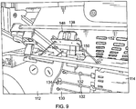
analyzer 168 and the subrack andtray PCBs cable 172 that connects theanalyzer 168 to thesubrack PCB 136. Also, power is supplied to the components on the subrack andtray PCBs analyzer 168 on thiscable 172. In one example, this connection is implemented as a RS422 serial connection. In this example, as shown inFIG. 9 , thesubrack PCB 136 includes twoconnectors 174 that can be used for connecting thecable 172 from theanalyzer 168 to thesubrack PCB 136. Also, these twoconnectors 174 can be oriented at an angle (for example, 30 degrees to 45 degrees) to facilitate routing thiscable 172 in a manner that is compatible with the fiber optic cables in therack 102. Either of the twoconnectors 174 can be used depending on what is more convenient for connecting to theanalyzer 168. Also, the twoconnectors 174 can be used to connectmultiple subracks 100 to theanalyzer 168 using a daisy chain topology. - As shown in
FIGS. 4 and10 , thetray 112 can includepockets 176 in the plastic of thetray 112 to accommodate components that are mounted to the underside of thetray PCB board 130. This enables thetray PCB 130 to lay flat in thetray 112. - In order to support a high density of
RFID antennas 132 andfiber optic adapters 114, it is helpful to be able to localize or constrain the field emitted from eachRFID antenna 134 so that only theappropriate RFID tag 128 is energized and read. One of example of how to do this is shown inFIG. 4 . The ground planes surround the conductive plane in which the RFID inductors (coil or antenna) are formed. Openings are formed in the upper ground plane in order to enable RF signals to pass between theRFID antenna 134 and anyRFID tag 128 positioned above it. The rest of the ground plane serves to constrain the RFID signals. Also, in this example, the openings formed in the bottom of the ground plane serve to let some of the RFID signals escape through the bottom to reduce the size of the field that is created above thetray PCB 130. -
FIG. 14 illustrates another way in which radio frequency fields emitted by RFID antennas can be constrained that is suitable for use in the exemplary subrack ofFIG. 1 . In the example shown inFIG. 14 , the layers of thetray PCB 130 are configured so that, for eachRFID antenna 132 on each tray 113, thetray PCB 130 includes amulti-layer coil assembly 1404 that implements thatRFID antenna 132. - The layers of the
tray PCB 130 are also configured so that, for eachRFID antenna 132 on each tray 113, thetray PCB 130 includes a respective C-shaped opencopper track feature 1402 and a respective O-shaped closedcopper track feature 1404 that concentrically surround thecoil assembly 1404. In the particular example shown inFIG. 14 , the C-shapedopen feature 1404 is located inside of the O-shapedclosed feature 1406. Eachrespective coil assembly 1402, C-shapedopen feature 1404, and O-shapedclosed feature 1406 are isolated from each another. - Each C-shaped
open feature 1402 provides a dampening field for producing a rectangular region of interest (ROI) box for addressing misalignment problems that may otherwise occur in general usage. Each C-shaped open feature 1042 also provides rear field dampening to thetray 112 below. Each O-shapedclosed features 1406 provides protection against cross-talk that may otherwise occur amongadjacent RFID antennas 132, where each such O-shapedclosed feature 1406 is implemented as shorted turn that produces a corresponding nulling field. - In some embodiments, it is necessary to position a
daughter board 200 onto thetray PCBs 130. For example, in some embodiments, a storage device (such as an EEPROM) is attached to each of thefiber optic connectors 116, which is read in the manner described in the United States Patent Applications cited above. This is done instead of using RFID technology to read RFID tags 128. One example of this type of technology is the QUAREO technology that is commercially available from TE Connectivity. This technology is also referred to here as "Connection Point Identifier" or "CPID" technology. - In this example (which can be implemented using QUAREO technology), the storage device interface comprises four leads -- a power lead, a ground lead, a data lead, and an extra lead that is reserved for future use. A suitable protocol (for example, the UNI/O protocol) can be used for communicating over the single data lead.
- In such an example, four contacts are positioned above each
adapter 114 that are configured to come into electrical contact with the four corresponding storage-device leads on a connector inserted in thatadapter 114. Appropriate traces are provided on thetray PCB 130 in thetray 112 to couple these adapter contacts to thetray controller 164 viamultiplexer 160 and to power and ground. The connectivity between thesubrack controller 162 and thetray controllers 164 is provided in the manner described above. In this way, the QUAREO (or similar CPID) technology can be integrated into what is otherwise anRFID subrack 100 to support the mixing and matching of CPID and RFID trays in the field. - The contacts for reading the storage devices (also referred to here as "CPID contacts" 220) can be attached to a daughter board 200 (shown in
FIGS. 12 and13 ). It is helpful to precisely align thisdaughter board 200 while attaching it to an appropriate daughter-board connector 202 on thetray PCB 136. One way of doing this is shown inFIGS. 12 and13 . One side of thedaughter board 200 has one ormore metal pins 204 extending from it. Thetray PCB 136 includes a correspondingplastic post 206. Thepins 204 andposts 206 are arranged so that eachpin 204 can be inserted into the top of a corresponding one of theposts 206 on thetray PCB 136. In this way, theconnectors daughterboard 200 andtray PCB 136 can more easily be connected while providing more precise alignment of the items on the daughter board 200 (for example, the interfaces for reading the EEPROMS, which in this example are positioned above thefiber optic adapters 114, which are preferably precisely aligned in order to read the EEPROMS). - Also, the
CPID contacts 220 can be placed on both sides of theadapters 114 so that either side of theadapters 114 can be used as the patch field in the manner described above connection with RFID versions of trays. In order to reduce the I/O pin count and trace routing complexity, for a givenadapter 114,CPID contacts 220 on both sides of theadapter 114 are coupled to thetray controller 164 and to power and ground using the same PCB traces. That is, a first set of PCB traces for coupling theCPID contacts 220 on the left side of eachadapter 114 and a second, separate set of PCB for coupling the CPID contacts 22- on the right side of thatadapter 114 need not be provided; instead, for eachadapter 114, only a single set of PCB traces need be provided for coupling theCPID contacts 220 on both sides of eachadapter 114 to thetray controller 164 and power and ground. - Although the preceding examples have been described above in connection with optical connectors and adapters, one of ordinary skill in the art can recognize that the techniques described here can be used with other types of communication media, such as copper communication media, connectors, and jacks and plugs (for example, those described in the United States Patent Applications described above).
- A number of embodiments have been described. Nevertheless, it will be understood that various modifications to the described embodiments may be made without departing from the scope of the claimed invention.
- Example 1 includes a tray for use in a subrack of a rack, the tray comprising: a printed circuit board configured so that a plurality of connections can be made at a plurality of positions on the printed circuit board, each of the plurality of connections involving at least one connector positioned on a patch side of the plurality of positions and the least one connector having a device associated therewith in which information is stored; wherein the tray is configured so that either side of the positions can be used as the patch side; and wherein the tray is configured so that the devices associated with the connectors involved in making the connections at the patch side can be read via the tray.
- Example 2 includes the tray of Example 1, wherein each of the plurality of connections involves at least one connector having an RFID tag associated therewith; and wherein the tray further comprises a plurality of pairs of RFID antennas, each pair of RFID antennas being associated with a respective one of the positions, wherein a respective one of each pair of RFID antennas is associated with each side; wherein the tray is configured so that the RFID antennas associated with the side used as the patch side are used to read the RFID tags associated with the connectors involved in making the connections.
- Example 3 includes the tray of Example 2, wherein each of the plurality of RFID antennas can be selectively coupled to an RFID reader in order to read the RFID tags associated with the connectors involved in making the connections.
- Example 4 includes the tray of Example 1, wherein each of the plurality of connections involves at least one connector having a connection point identifier (CPID) storage device associated therewith, the CPID storage device comprising one or more contacts used for reading the CPID storage device; and wherein the tray further comprises a plurality of pairs of contacts, each pair of contacts being associated with a respective one of the positions; wherein the tray is configured so that contacts of the tray associated with the side used as the patch side are used to read the CPID storage devices associated with the connectors involved in making the connections.
- Example 5 includes the tray of any of the Examples 1-4, further comprising a plurality of pairs of visual indicators each pair of visual indicators being associated with a respective one of the positions, wherein a respective one of the pair of visual indicators is associated with a respective side of the positions.
- Example 6 includes the tray of Example 5, wherein at least some of the visual indicators comprise a light emitting diode.
- Example 7 includes the tray of any of the Examples 1-6, wherein the printed circuit board is configured so that a plurality of fiber optic adapters can be attached to the printed circuit board, each of the plurality of fiber optic adapters associated with a respective one of the positions.
- Example 8 includes the tray of Example 7, wherein a plurality of clips is attached to the printed circuit board so that each of the plurality of fiber optic adapters can be removably attached to the printed circuit board.
- Example 9 includes the tray of any of the Examples 1-8, further comprising: a tray controller; at least two communication ports each of which is coupled to the tray controller, wherein the tray is configured so that the tray controller can be coupled to a controller external to the tray via one or more of the communication ports.
- Example 10 includes the tray of Example 9, wherein the communication ports are angled.
- Example 11 includes the tray of any of the Examples 1-10, wherein the each of the plurality of connections is made using at least one of optical cabling and metallic cabling.
- Example 12 includes the tray of any of the Examples 1-11, wherein the tray includes pockets formed in the tray to accommodate components.
- Example 13 includes a method of using a tray, the tray comprising a printed circuit board configured so that a plurality of connections can be made at a plurality of positions on the printed circuit board, each of the positions having at least two sides, wherein the method comprises: selecting one of the sides as a patch side; making the plurality of connections using the tray, each of the plurality of connections involving at least one connector having a device associated therewith in which information is stored and wherein the selected patch side is used as the patch side for each of the plurality of connections; and reading, via the tray, information stored in the devices associated with the connectors involved in making the connections.
- Example 14 includes the method of Example 13, wherein each of the plurality of connections involves at least one connector having an RFID tag associated therewith; and wherein the tray further comprises a plurality of pairs of RFID antennas, each pair of RFID antennas being associated with a respective one of the positions, wherein a respective one of the pair of RFID antennas is associated with a respective side of the positions; and wherein reading, via the tray, information stored in the devices associated with the connectors involved in making the connections comprises: reading the RFID tags associated with the connectors involved in making the connections using the RFID antennas associated with the selected patch side.
- Example 15 includes the method of Example 14, further comprising selectively coupling each of the plurality of RFID antennas to an RFID reader in order to read any RFID tag associated with the connector involved in making the associated connection.
- Example 16 includes the method of Example 13, wherein each of the plurality of connections involves at least one connector having a connection point identifier (CPID) storage device associated therewith, the CPID storage device comprising one or more contacts used for reading the CPID storage device; and wherein the tray further comprises a plurality of pairs of contacts, each pair of contacts being associated with a respective one of the positions; and wherein reading, via the tray, information stored in the devices associated with the connectors involved in making the connections comprises: reading the CPID storage devices associated with the connectors involved in making the connections using the contacts of the tray associated with the selected patch side.
- Example 17 includes the method of any of the Examples 13-16, wherein the tray further comprises a plurality of pairs of visual indicators, each pair of visual indicators being associated with a respective one of the positions, wherein a respective one of the pair of visual indicators is associated with a respective side of the positions; and wherein the method further comprises providing visual indications using the visual indicators using the visual indicators associated with the selected patch side.
- Example 18 includes the method of any of the Examples 13-17, wherein the printed circuit board is configured so that a plurality of fiber optic adapters can be attached to the printed circuit board, each of the plurality of fiber optic adapters associated with a respective one of the positions.
- Example 19 includes the method of Example 18, further comprising removably attaching each of the plurality of fiber optic adapters to the tray.
- Example 20 includes a subrack comprising: a backplate; at least one tray configured so that a plurality of connections can be made at a plurality of positions on the tray, each of the plurality of connections involving at least one connector having information stored in a device associated therewith that can be read; wherein the backplate and the tray are configured so that the tray can be selectively attached and removed from the backplate; and wherein the backplate and the tray are configured so that the devices associated with the connectors involved in making the connections can be read via the tray.
- Example 21 includes the subrack of Example 20, wherein the devices associated with each connector comprises RFID tags, wherein the backplate and the tray are configured so that the RFID tags associated with the connectors involved in making the connections can be read via the tray.
- Example 22 includes the subrack of Example 21, wherein each tray comprises a plurality of RFID antennas, each of the RFID antennas being associated with a respective one of the positions, wherein each of the plurality of RFID antennas can be selectively coupled to an RFID reader in order to read the RFID tags associated with the connectors involved in making the connections.
- Example 23 includes the subrack of Example 20, wherein the devices associated each connector comprises connection point identifier (CPID) storage devices, wherein the backplate and the tray are configured so that the CPID storage devices associated with the connectors involved in making the connections can be read via the tray.
- Example 24 includes the subrack of any of the Examples 20 to 23, wherein the backplate is implemented as a backplane printed circuit board.
- Example 25 includes the subrack of Example 24, wherein the backplane printed circuit board comprises a tray connector, wherein the tray has attached thereto a backplane connector that is configured to be connected to the tray connector of the backplane printed circuit board in connection with the tray being attached to the backplate; and wherein the tray further comprises at least one plastic tether attached to the backplane connector, wherein the plastic tether is configured to pull the backplane connector out of the tray connector on the backplane printed circuit board in connection with the tray being removed from the backplate.
- Example 26 includes the subrack of any of the Examples 24 or 25, wherein the backplane printed circuit board comprises at least one cut out to which a strain relief cable can be attached.
- Example 27 includes the subrack of any of the Examples 20 to 26, further comprising a plurality of trays.
- Example 28 includes the subrack of any of the Examples 20 to 27 wherein each tray comprises a plurality of visual indicators, each of the visual indicators being associated with a respective one of the positions.
- Example 29 includes the subrack of any of the Examples 20 to 28, wherein each tray is configured so that a plurality of fiber optic adapters can be attached to the printed circuit board, each of the plurality of fiber optic adapters associated with a respective one of the positions.
- Example 30 includes the subrack of any of the Examples 20 to 29, further comprising a subrack controller, wherein each tray comprises: a tray controller; and at least two communication ports, each of which is coupled to the tray controller, wherein the subrack is configured so that the tray controller can be coupled to the subrack controller via one or more of the communication ports.
- Example 31 includes the subrack of Example 30, wherein the communication ports are angled.
- Example 32 includes the subrack of any of the Examples 20 to 31, wherein each tray includes pockets formed in the tray to accommodate electronics.
- Example 33 includes the subrack of any of the Examples 20 to 32, wherein the each of the plurality of connections is made using at least one of optical cabling and metallic cabling.
- Example 34 includes a method of using a subrack that comprises a backplate and at least one tray configured so that a plurality of connections can be made at a plurality of positions on the tray, each of the plurality of connections involving at least one connector having information stored in a device associated therewith, the method comprising: attaching the tray to the backplate; reading, via the tray, the devices associated with the connectors involved in making the connections; and removing the tray from the backplate and thereafter re-attaching the tray to the backplate.
- Example 35 includes the method of Example 34, wherein the devices associated each connector comprises RFID tags; and wherein reading, via the tray, the devices associated with the connectors involved in making the connections comprises reading, via the tray, the RFID tags associated with the connectors involved in making the connections.
- Example 36 includes the method of Example 35, wherein each tray comprises a plurality of RFID antennas, each of the RFID antennas being associated with a respective one of the positions; and wherein reading the RFID tags associated with the connectors involved in making the connections via the tray comprises selectively coupling each of the plurality of RFID antennas to an RFID reader in order to read the RFID tags associated with the connectors involved in making the connections.
- Example 37 includes the method of Example 34, wherein the devices associated each connector comprises connection point identifier (CPID) storage devices; and wherein reading, via the tray, the devices associated with the connectors involved in making the connections comprises reading the CPID storage devices associated with the connectors involved in making the connections via the tray.
- Example 38 includes the method of any of the Examples 34 to 37, wherein the backplate is implemented as a backplane printed circuit board.
- Example 39 includes the method of Example 38, wherein the backplane printed circuit board comprises a tray connector, wherein the tray has attached thereto a backplane connector that is configured to be connected to the tray connector of the backplane printed circuit board in connection with the tray being attached to the backplate; and wherein the tray further comprises at least one plastic tether attached to the backplane connector, wherein the plastic tether is configured to pull the backplane connector out of the tray connector on the backplane printed circuit board in connection with the tray being removed from the backplate.
- Example 40 includes the method of any of the Examples 38 to 39, further comprising attaching a strain relief cable to the tray using a cut out formed in the backplane printed circuit board.
- Example 41 includes a tray for use in a subrack of a rack, the tray comprising: a printed circuit board configured so that a plurality of connections can be made at a plurality of positions on the printed circuit board, each of the plurality of connections involving at least one connector having an RFID tag associated therewith; a plurality of RFID antennas integrated into the printed circuit board, each the RFID antennas associated with a respective one of the positions; and wherein the printed circuit board is configured to localize a field emitted from each RFID antenna so that only the RFID tag associated with that RFID antenna is energized and read.
- Example 42 includes the tray of Example 41, wherein the printed circuit board comprises a conductive plane surrounded on an upper side by a first ground plane and surrounded on a bottom side by a second ground plane; and wherein the RFID antennas are formed in the conductive layer of the printed circuit board.
- Example 43 includes the tray Example 42, wherein, for each RFID antenna, a respective opening is formed in the upper ground plane so that radio frequency signals can pass between the respective RFID antenna and any RFID tag positioned near the opening, wherein the rest of the ground plane is configured to constrain the radio frequency signals emitted from the RFID antennas.
- Example 44 includes the tray of Example 43, wherein, for each RFID antenna, a respective opening is formed in the bottom ground plane so that radio frequency signals can escape out through the respective opening in the bottom ground plane in order to reduce the size of the field created above the printed circuit board.
- Example 45 includes the tray of any of the Examples 41-44, wherein the tray includes pockets formed in the tray to accommodate electronics.
- Example 46 includes the tray of any of the Examples 41-45, wherein the tray comprises at least one of: a plurality of RFID antennas, each of the RFID antennas being associated with a respective one of the positions, wherein each of the plurality of RFID antennas can be selectively coupled to an RFID reader in order to read the RFID tags associated with the connectors involved in making the connections; and a plurality of visual indicators, each of the visual indicators being associated with a respective one of the positions.
- Example 47 includes the tray of any of the Examples 41-46, wherein the tray is configured so that a plurality of fiber optic adapters can be attached to the printed circuit board, each of the plurality of fiber optic adapters associated with a respective one of the positions.
- Example 48 includes the tray of any of the Examples 41-47, further comprising: a tray controller; and at least two communication ports, each of which is coupled to the tray controller, wherein the tray is configured so that the tray controller can be coupled to a controller external to the tray via one or more of the communication ports.
- Example 49 includes the tray of Example 48, wherein the communication ports are angled.
- Example 50 includes the tray of any of the Examples 41-49, wherein the each of the plurality of connections is made using between at least one of optical cabling and metallic cabling.
- Example 51 includes the tray of any of the Examples 41-50, wherein the each of the plurality of connections is made using at least one of optical cabling and metallic cabling.
- Example 52 includes a method of using a tray, the tray comprising a printed circuit board and a plurality of RFID antennas integrated into the printed circuit board, each the RFID antennas associated with a respective one of a plurality of positions on the printed circuit board, the method comprising: making a plurality of connections at the plurality of positions on the printed circuit board, each of the plurality of connections involving at least one connector having an RFID tag associated therewith; energizing and reading the RFID tags using the RFID antennas; and localizing a field emitted from each RFID antenna so that only the RFID tag associated with that RFID antenna is energized and read.
- Example 53 includes the method of Example 52, wherein the printed circuit board comprises a conductive plane surrounded on an upper side by a first ground plane and surrounded on a bottom side by a second ground plane; and wherein the RFID antennas are formed in the conductive layer of the printed circuit board.
- Example 54 includes the method of Example 53, wherein, for each RFID antenna, a respective opening is formed in the upper ground plane so that radio frequency signals can pass between the respective RFID antenna and any RFID tag positioned near the opening, wherein the rest of the ground plane is configured to constrain the radio frequency signals emitted from the RFID antennas.
- Example 55 includes the method of Example 54, wherein, for each RFID antenna, a respective opening is formed in the bottom ground plane so that radio frequency signals can escape out through the respective opening in the bottom ground plane in order to reduce the size of the field created above the printed circuit board.
Claims (15)
- A tray (112) for use in a subrack (100) of a rack, the tray (112) comprising:a printed circuit board (130) configured so that a plurality of connections can be made at a plurality of positions (114) on the printed circuit board (130), each of the plurality of connections involving at least one connector (116) positioned on a patch side of the plurality of positions (114) and the least one connector (116) having a device (128) associated therewith in which information is stored, where each of the plurality of connections is made using at least one of optical cabling and metallic cabling; and wherein the tray (112) is configured so that either side of the positions (114) can be used as the patch side;characterized in thatthe tray (112) is configured so that the devices (128) associated with the connectors (116) involved in making the connections at the patch side can be read via the tray (112) from whichever side of the positions (114) is selected as the patch side.
- The tray according to claim 1, wherein the subrack (100) includes a backplate (110) that extends vertically and is adapted to receive a plurality of vertically stacked trays (112);
wherein the tray (112) is configured to be rotatably mounted to the backplane (110) of the subrack (100) so that it can be flipped up, preferably, wherein the tray (112) is configured to be removably mounted to the backplate (110). - The tray according to claim 1 or 2, wherein each device (128) comprises an RFID tag (128); and
wherein the tray (112) further comprises a plurality of pairs of RFID antennas (132), each pair of RFID antennas (132) being associated with a respective one of the positions (114), wherein a respective one of each pair of RFID antennas (132) is associated with each side of the positions (114);
wherein the tray (112) is further configured so that the RFID antennas (132) associated with the side of the positions (114) used as the patch side are used to read the RFID tags (128) associated with the connectors (116) involved in making the connections. - The tray according to claim 3, wherein the printed circuit board (130) is configured to localize a field emitted from each RFID antenna (132) so that only the RFID tag (128) associated with that RFID antenna (132) is energized and read.
- The tray according to claim 4, wherein the printed circuit board (130) comprises a conductive plane surrounded on an upper side by a first ground plane and surrounded on a bottom side by a second ground plane; and
wherein the RFID antennas (132) are formed in the conductive layer of the printed circuit board (130). - The tray according to claim 5, wherein, for each RFID antenna (132), a respective opening is formed in the first ground plane so that radio frequency signals can pass between the respective RFID antenna (132) and any RFID tag (128) positioned near the opening, wherein the rest of the first ground plane is configured to constrain the radio frequency signals emitted from the RFID antennas (132), preferably, wherein, for each RFID antenna (132), a respective opening is formed in the second ground plane so that radio frequency signals can escape out through the respective opening in the second ground plane in order to reduce the size of the field created above the printed circuit board (130).
- The tray according to any of claims 3 to 6, wherein each RFID antenna (132) can be selectively coupled to an RFID reader (156) in order to read the RFID tags (128) associated with the connectors (116) involved in making the connections.
- The tray according to claim 1 or 2, wherein each of the plurality of connections involves at least one connector (116) having a connection point identifier (CPID) storage device associated therewith, the CPID storage device comprising one or more contacts used for reading the CPID storage device; and
wherein the tray (112) further comprises a plurality of pairs of contacts (208), each pair of contacts (208) being associated with a respective one of the positions (114);
wherein the tray (112) is configured so that contacts (208) of the tray (112) associated with the side used as the patch side are used to read the CPID storage devices associated with the connectors (116) involved in making the connections. - The tray according to any of claims 1 to 8, further comprising a plurality of pairs of visual indicators (134), each pair of visual indicators (134) being associated with a respective one of the positions (114), wherein a respective one of the pair of visual indicators (134) is associated with a respective side of the positions (114), preferably, wherein at least some of the visual indicators (134) comprise a light emitting diode.
- The tray according to any of claims 1 to 9, wherein the printed circuit board (130) is configured so that a plurality of fiber optic adapters can be attached to the printed circuit board, each of the plurality of fiber optic adapters associated with a respective one of the positions (114), preferably, a plurality of clips (120) are attached to the printed circuit board (130) so that each of the plurality of fiber optic adapters can be removably attached to the printed circuit board (130).
- The tray according to any of claims 1 to 11, further comprising:a tray controller (164); andat least two communication ports each of which is coupled to the tray controller (164), wherein the tray (112) is configured so that the tray controller (164) can be coupled to a an external controller via one or more of the communication ports, preferably, the communication ports are angled.
- The tray according to any of claims 1 to 11, wherein the tray (112) includes pockets (176) formed in the tray (112) to accommodate components.
- A method of using a tray (112), the tray (112) comprising a printed circuit board (130) configured so that a plurality of connections can be made at a plurality of positions (114) on the printed circuit board (130), each of the positions (114) having at least two sides, wherein the method comprises:selecting one of the sides as a patch side; andmaking the plurality of connections using the tray (112), each of the plurality of connections involving at least one connector (116) having a device (128) associated therewith in which information is stored and wherein the selected patch side is used as the patch side for each of the plurality of connections;characterized in thatthe method further comprises reading, via the tray (112) from whichever side of the positions (114) is selected as the patch side, information stored in the devices (128) associated with the connectors (116) involved in making the connections.
- The method according to claim 13, wherein the tray (112) is used in a subrack (100) that includes a backplate (100) that extends vertically and is adapted to receive a plurality of vertically stacked trays (112);
wherein the method further comprises mounting the tray (112) to the backplate (110) of the subrack (100);
wherein the tray (112) is rotatably mounted to the backplate (110) of the subrack (100) so that it can be flipped up, preferably, wherein the tray (112) is removably mounted to the backplate (110). - The method according to claim 13 or 14, wherein the backplate (110) of the subrack (100) receives a plurality of vertically stacked trays (112), preferably the backplate (110) is disposed at an angle relative to the vertical so that the plurality of trays (112) is arranged in a stair step configuration, the method further comprising flipping up a first tray (112) in order to provide access to a second tray (112) that is underneath the first tray (112).
Applications Claiming Priority (2)
| Application Number | Priority Date | Filing Date | Title |
|---|---|---|---|
| US201261598713P | 2012-02-14 | 2012-02-14 | |
| PCT/EP2013/000441 WO2013120616A2 (en) | 2012-02-14 | 2013-02-14 | Physical layer management (plm) in an optical distribution frame |
Publications (2)
| Publication Number | Publication Date |
|---|---|
| EP2815587A2 EP2815587A2 (en) | 2014-12-24 |
| EP2815587B1 true EP2815587B1 (en) | 2017-10-18 |
Family
ID=47843227
Family Applications (1)
| Application Number | Title | Priority Date | Filing Date |
|---|---|---|---|
| EP13708082.6A Active EP2815587B1 (en) | 2012-02-14 | 2013-02-14 | Physical layer management (plm) in an optical distribution frame |
Country Status (9)
| Country | Link |
|---|---|
| US (3) | US9111249B2 (en) |
| EP (1) | EP2815587B1 (en) |
| CN (1) | CN104380759B (en) |
| AU (1) | AU2013220736B2 (en) |
| BR (1) | BR112014020121A2 (en) |
| CL (1) | CL2014002161A1 (en) |
| MX (1) | MX336311B (en) |
| NZ (1) | NZ628612A (en) |
| WO (1) | WO2013120616A2 (en) |
Families Citing this family (22)
| Publication number | Priority date | Publication date | Assignee | Title |
|---|---|---|---|---|
| US9111249B2 (en) * | 2012-02-14 | 2015-08-18 | Tyco Electronics Uk Ltd | Physical layer management (PLM) system for use with an optical distribution frame using RFID antennas with localized fields |
| CN102752672B (en) * | 2012-06-06 | 2015-07-08 | 华为技术有限公司 | Method, device and system for optical fiber distribution |
| WO2014049361A1 (en) | 2012-09-27 | 2014-04-03 | Tyco Electronics Uk Ltd. | Mobile application for assisting a technician in carrying out an electronic work order |
| WO2014076198A2 (en) | 2012-11-16 | 2014-05-22 | Tyco Electronics Uk Ltd. | Localized reading of rfid tags and rfid managed connectivity |
| CN203444504U (en) * | 2013-08-26 | 2014-02-19 | 鸿富锦精密工业(深圳)有限公司 | Reader |
| EP3042355A4 (en) | 2013-09-04 | 2017-04-19 | CommScope Technologies LLC | Physical layer system with support for multiple active work orders and/or multiple active technicians |
| US9279945B2 (en) | 2014-02-10 | 2016-03-08 | Avago Technologies General Ip (Singapore) Pte. Ltd. | Methods, apparatuses and systems for blind mating arrays of multi-optical fiber connector modules |
| CN106461897B (en) * | 2014-02-14 | 2020-01-21 | 泰科电子英国有限公司 | Managed Connections for Optical Patch Panels |
| US9258916B2 (en) * | 2014-03-07 | 2016-02-09 | Go!Foton Holdings, Inc. | High density cassette storage system |
| CN204129294U (en) * | 2014-09-17 | 2015-01-28 | 中兴通讯股份有限公司 | A kind of fiber optic network distributing equipment |
| US9451716B1 (en) * | 2015-06-27 | 2016-09-20 | Intel Corporation | Serviceable chassis for devices |
| EP3360290B1 (en) | 2015-10-08 | 2022-11-02 | Commscope Technologies LLC | Communication media and methods for providing indication of signal power to a network entity |
| KR102460453B1 (en) * | 2016-02-19 | 2022-10-28 | 삼성전자주식회사 | Electronic device attachable outside storage media |
| US10346654B2 (en) | 2016-10-05 | 2019-07-09 | Mox Networks, LLC | RFID-based rack inventory management systems |
| WO2018195588A1 (en) * | 2017-04-26 | 2018-11-01 | The Yield Technology Solutions Pty Ltd | An electronics holder |
| CN107404673A (en) * | 2017-08-31 | 2017-11-28 | 苏州惠华电子科技有限公司 | A kind of electronic wiring frame of the RFID based on EMI |
| CN107529099A (en) * | 2017-08-31 | 2017-12-29 | 苏州惠华电子科技有限公司 | A kind of electrical harnesses frame control system based on RFID |
| CN110049652B (en) * | 2018-01-16 | 2021-07-09 | 联想企业解决方案(新加坡)有限公司 | Server racks and cabinets including server racks |
| CN208705520U (en) * | 2018-09-25 | 2019-04-05 | 中兴通讯股份有限公司 | Fiber splicing tray |
| US11353662B2 (en) * | 2019-04-26 | 2022-06-07 | Hewlett Packard Enterprise Development Lp | Smart carriers and smart adapters for automatic discovery of fiber assemblies |
| US11464131B2 (en) * | 2020-02-07 | 2022-10-04 | Seagate Technology Llc | Cable management assembly |
| CN111511139B (en) * | 2020-04-30 | 2021-03-16 | 陇东学院 | A new type of multifunctional maintenance device for electrical automation |
Family Cites Families (43)
| Publication number | Priority date | Publication date | Assignee | Title |
|---|---|---|---|---|
| US5910776A (en) | 1994-10-24 | 1999-06-08 | Id Technologies, Inc. | Method and apparatus for identifying locating or monitoring equipment or other objects |
| CA2162515C (en) | 1994-12-22 | 2000-03-21 | Leonard George Cohen | Jumper tracing system |
| EP0917377B1 (en) | 1997-11-11 | 2007-07-04 | CCS Technology, Inc. | Method for managing and documentation of contact points of a wiring network |
| US6002331A (en) | 1998-07-20 | 1999-12-14 | Laor; Herzel | Method and apparatus for identifying and tracking connections of communication lines |
| US6499861B1 (en) | 1999-09-23 | 2002-12-31 | Avaya Technology Corp. | Illuminated patch cord connector ports for use in a telecommunications patch closet having patch cord tracing capabilities |
| US6784802B1 (en) | 1999-11-04 | 2004-08-31 | Nordx/Cdt, Inc. | Real time monitoring of cable patch panel |
| JP3925032B2 (en) | 2000-03-14 | 2007-06-06 | 富士ゼロックス株式会社 | Printed wiring board |
| US6808116B1 (en) | 2002-05-29 | 2004-10-26 | At&T Corp. | Fiber jumpers with data storage method and apparatus |
| US6882525B2 (en) | 2003-02-27 | 2005-04-19 | Storcase Technology, Inc. | Universal receptacles for interchangeably receiving different removable computer drive carriers |
| US6847856B1 (en) | 2003-08-29 | 2005-01-25 | Lucent Technologies Inc. | Method for determining juxtaposition of physical components with use of RFID tags |
| US7046899B2 (en) | 2004-03-02 | 2006-05-16 | Furukawa Electric North America, Inc. | Universal apparatus for incorporating intelligence into an optical fiber distribution frame |
| US7197214B2 (en) | 2004-05-24 | 2007-03-27 | Corning Cable Systems Llc | Methods and apparatus for facilitating cable locating |
| US7246746B2 (en) | 2004-08-03 | 2007-07-24 | Avaya Technology Corp. | Integrated real-time automated location positioning asset management system |
| AU2005314108A1 (en) | 2004-12-06 | 2006-06-15 | Commscope, Inc. Of North Carolina | Telecommunications patching system that utilizes RFID tags to detect and identify patch cord interconnections |
| US7403396B2 (en) | 2005-01-20 | 2008-07-22 | Hewlett-Packard Development Company, L.P. | Communicating with an electronic module that is slidably mounted in a system |
| US8050939B2 (en) | 2005-02-11 | 2011-11-01 | Avaya Inc. | Methods and systems for use in the provision of services in an institutional setting such as a healthcare facility |
| US7468669B1 (en) | 2005-06-21 | 2008-12-23 | Avaya Technology Corp. | RFID patch panels and cables |
| US7406231B1 (en) | 2005-06-21 | 2008-07-29 | Avaya Technology Corp. | Electroluminescent patch cable |
| US7772975B2 (en) | 2006-10-31 | 2010-08-10 | Corning Cable Systems, Llc | System for mapping connections using RFID function |
| US7782202B2 (en) | 2006-10-31 | 2010-08-24 | Corning Cable Systems, Llc | Radio frequency identification of component connections |
| US8264366B2 (en) | 2009-03-31 | 2012-09-11 | Corning Incorporated | Components, systems, and methods for associating sensor data with component location |
| US8116434B2 (en) | 2006-11-29 | 2012-02-14 | Commscope, Inc. Of North Carolina | Telecommunications patching system that facilitates detection and identification of patch cords |
| US7760094B1 (en) | 2006-12-14 | 2010-07-20 | Corning Cable Systems Llc | RFID systems and methods for optical fiber network deployment and maintenance |
| US8264355B2 (en) | 2006-12-14 | 2012-09-11 | Corning Cable Systems Llc | RFID systems and methods for optical fiber network deployment and maintenance |
| US7667574B2 (en) | 2006-12-14 | 2010-02-23 | Corning Cable Systems, Llc | Signal-processing systems and methods for RFID-tag signals |
| US7965186B2 (en) | 2007-03-09 | 2011-06-21 | Corning Cable Systems, Llc | Passive RFID elements having visual indicators |
| US7547150B2 (en) | 2007-03-09 | 2009-06-16 | Corning Cable Systems, Llc | Optically addressed RFID elements |
| US7855697B2 (en) | 2007-08-13 | 2010-12-21 | Corning Cable Systems, Llc | Antenna systems for passive RFID tags |
| US8203450B2 (en) | 2008-01-02 | 2012-06-19 | Commscope, Inc. | Intelligent MPO-to-MPO patch panels having connectivity tracking capabilities and related methods |
| US8138925B2 (en) | 2008-01-15 | 2012-03-20 | Corning Cable Systems, Llc | RFID systems and methods for automatically detecting and/or directing the physical configuration of a complex system |
| US8181229B2 (en) | 2008-03-25 | 2012-05-15 | Commscope, Inc. Of North Carolina | Methods, systems and computer program products for operating a communications network with enhanced security |
| US8248208B2 (en) | 2008-07-15 | 2012-08-21 | Corning Cable Systems, Llc. | RFID-based active labeling system for telecommunication systems |
| US7856166B2 (en) | 2008-09-02 | 2010-12-21 | Corning Cable Systems Llc | High-density patch-panel assemblies for optical fiber telecommunications |
| US7729586B2 (en) | 2008-10-07 | 2010-06-01 | Commscope Inc. Of North Carolina | Telecommunications patching systems with vertically-oriented patching modules |
| WO2010096544A1 (en) | 2009-02-19 | 2010-08-26 | Commscope Inc. Of North Carolina | Patch panel cable information detection systems and methods |
| CN101521575B (en) | 2009-04-09 | 2011-01-05 | 华为终端有限公司 | Method, control point, equipment and communication system for collocating accessing authority |
| US8075348B2 (en) | 2009-04-23 | 2011-12-13 | Commscope Inc. Of North Carolina | Assembly and system of datacommunication cables and connectors |
| US8478099B2 (en) | 2009-11-13 | 2013-07-02 | Reflex Photonics Inc. | Optical backplane rack assembly with external optical connectors |
| US8172468B2 (en) | 2010-05-06 | 2012-05-08 | Corning Incorporated | Radio frequency identification (RFID) in communication connections, including fiber optic components |
| US20110273892A1 (en) * | 2010-05-07 | 2011-11-10 | Tyco Electronics Corporation | Solid state lighting assembly |
| US8410909B2 (en) | 2010-07-09 | 2013-04-02 | Corning Incorporated | Cables and connector assemblies employing a furcation tube(s) for radio-frequency identification (RFID)-equipped connectors, and related systems and methods |
| US8582302B2 (en) | 2011-11-15 | 2013-11-12 | Microsoft Corporation | Modular equipment rack system for data center |
| US9111249B2 (en) | 2012-02-14 | 2015-08-18 | Tyco Electronics Uk Ltd | Physical layer management (PLM) system for use with an optical distribution frame using RFID antennas with localized fields |
-
2013
- 2013-02-13 US US13/766,151 patent/US9111249B2/en active Active
- 2013-02-13 US US13/766,120 patent/US9805332B2/en not_active Expired - Fee Related
- 2013-02-13 US US13/766,137 patent/US9361600B2/en not_active Expired - Fee Related
- 2013-02-14 WO PCT/EP2013/000441 patent/WO2013120616A2/en not_active Ceased
- 2013-02-14 NZ NZ628612A patent/NZ628612A/en not_active IP Right Cessation
- 2013-02-14 CN CN201380019932.4A patent/CN104380759B/en not_active Expired - Fee Related
- 2013-02-14 EP EP13708082.6A patent/EP2815587B1/en active Active
- 2013-02-14 MX MX2014009775A patent/MX336311B/en unknown
- 2013-02-14 BR BR112014020121A patent/BR112014020121A2/en not_active IP Right Cessation
- 2013-02-14 AU AU2013220736A patent/AU2013220736B2/en not_active Ceased
-
2014
- 2014-08-13 CL CL2014002161A patent/CL2014002161A1/en unknown
Non-Patent Citations (1)
| Title |
|---|
| None * |
Also Published As
| Publication number | Publication date |
|---|---|
| MX336311B (en) | 2016-01-13 |
| CL2014002161A1 (en) | 2015-06-05 |
| CN104380759B (en) | 2018-07-03 |
| AU2013220736A1 (en) | 2014-09-04 |
| MX2014009775A (en) | 2014-11-25 |
| EP2815587A2 (en) | 2014-12-24 |
| BR112014020121A2 (en) | 2019-09-24 |
| US20130207782A1 (en) | 2013-08-15 |
| WO2013120616A3 (en) | 2013-10-10 |
| US20130205579A1 (en) | 2013-08-15 |
| AU2013220736B2 (en) | 2017-05-11 |
| US9111249B2 (en) | 2015-08-18 |
| WO2013120616A2 (en) | 2013-08-22 |
| US9805332B2 (en) | 2017-10-31 |
| CN104380759A (en) | 2015-02-25 |
| NZ628612A (en) | 2016-06-24 |
| US9361600B2 (en) | 2016-06-07 |
| US20130306723A1 (en) | 2013-11-21 |
Similar Documents
| Publication | Publication Date | Title |
|---|---|---|
| EP2815587B1 (en) | Physical layer management (plm) in an optical distribution frame | |
| US12235505B2 (en) | Fiber optic cassette arrangement | |
| US10871618B2 (en) | Connectivity appliance | |
| US10101542B2 (en) | Managed connectivity systems | |
| US20100079248A1 (en) | Optical fiber connector assembly with wire-based RFID antenna | |
| US20150060539A1 (en) | Telecommunications systems with managed connectivity | |
| US20130195396A1 (en) | Optical physical interface module | |
| US9995883B2 (en) | Optical adapter module with managed connectivity | |
| US7636506B2 (en) | Optical fiber management in a chassis-based network system | |
| US10101551B2 (en) | Multi-core/single-core conversion module and multi-core/single-core conversion apparatus | |
| US20200341201A1 (en) | Smart carriers and smart adapters for automatic discovery of fiber assemblies |
Legal Events
| Date | Code | Title | Description |
|---|---|---|---|
| PUAI | Public reference made under article 153(3) epc to a published international application that has entered the european phase |
Free format text: ORIGINAL CODE: 0009012 |
|
| 17P | Request for examination filed |
Effective date: 20140912 |
|
| AK | Designated contracting states |
Kind code of ref document: A2 Designated state(s): AL AT BE BG CH CY CZ DE DK EE ES FI FR GB GR HR HU IE IS IT LI LT LU LV MC MK MT NL NO PL PT RO RS SE SI SK SM TR |
|
| AX | Request for extension of the european patent |
Extension state: BA ME |
|
| DAX | Request for extension of the european patent (deleted) | ||
| GRAP | Despatch of communication of intention to grant a patent |
Free format text: ORIGINAL CODE: EPIDOSNIGR1 |
|
| INTG | Intention to grant announced |
Effective date: 20170616 |
|
| GRAS | Grant fee paid |
Free format text: ORIGINAL CODE: EPIDOSNIGR3 |
|
| GRAA | (expected) grant |
Free format text: ORIGINAL CODE: 0009210 |
|
| AK | Designated contracting states |
Kind code of ref document: B1 Designated state(s): AL AT BE BG CH CY CZ DE DK EE ES FI FR GB GR HR HU IE IS IT LI LT LU LV MC MK MT NL NO PL PT RO RS SE SI SK SM TR |
|
| REG | Reference to a national code |
Ref country code: GB Ref legal event code: FG4D |
|
| REG | Reference to a national code |
Ref country code: CH Ref legal event code: EP |
|
| REG | Reference to a national code |
Ref country code: AT Ref legal event code: REF Ref document number: 938887 Country of ref document: AT Kind code of ref document: T Effective date: 20171115 Ref country code: IE Ref legal event code: FG4D |
|
| REG | Reference to a national code |
Ref country code: DE Ref legal event code: R096 Ref document number: 602013028065 Country of ref document: DE |
|
| REG | Reference to a national code |
Ref country code: DE Ref legal event code: R081 Ref document number: 602013028065 Country of ref document: DE Owner name: COMMSCOPE CONNECTIVITY BELGIUM BVBA, BE Free format text: FORMER OWNER: TYCO ELECTRONICS RAYCHEM BVBA, KESSEL-LO, BE Ref country code: DE Ref legal event code: R081 Ref document number: 602013028065 Country of ref document: DE Owner name: COMMSCOPE CONNECTIVITY UK LTD., SWINDON, GB Free format text: FORMER OWNER: TYCO ELECTRONICS RAYCHEM BVBA, KESSEL-LO, BE Ref country code: DE Ref legal event code: R082 Ref document number: 602013028065 Country of ref document: DE Representative=s name: MURGITROYD & COMPANY, DE |
|
| REG | Reference to a national code |
Ref country code: NL Ref legal event code: MP Effective date: 20171018 |
|
| REG | Reference to a national code |
Ref country code: FR Ref legal event code: PLFP Year of fee payment: 6 |
|
| REG | Reference to a national code |
Ref country code: LT Ref legal event code: MG4D |
|
| REG | Reference to a national code |
Ref country code: AT Ref legal event code: MK05 Ref document number: 938887 Country of ref document: AT Kind code of ref document: T Effective date: 20171018 |
|
| PG25 | Lapsed in a contracting state [announced via postgrant information from national office to epo] |
Ref country code: NL Free format text: LAPSE BECAUSE OF FAILURE TO SUBMIT A TRANSLATION OF THE DESCRIPTION OR TO PAY THE FEE WITHIN THE PRESCRIBED TIME-LIMIT Effective date: 20171018 |
|
| PG25 | Lapsed in a contracting state [announced via postgrant information from national office to epo] |
Ref country code: NO Free format text: LAPSE BECAUSE OF FAILURE TO SUBMIT A TRANSLATION OF THE DESCRIPTION OR TO PAY THE FEE WITHIN THE PRESCRIBED TIME-LIMIT Effective date: 20180118 Ref country code: ES Free format text: LAPSE BECAUSE OF FAILURE TO SUBMIT A TRANSLATION OF THE DESCRIPTION OR TO PAY THE FEE WITHIN THE PRESCRIBED TIME-LIMIT Effective date: 20171018 Ref country code: SE Free format text: LAPSE BECAUSE OF FAILURE TO SUBMIT A TRANSLATION OF THE DESCRIPTION OR TO PAY THE FEE WITHIN THE PRESCRIBED TIME-LIMIT Effective date: 20171018 Ref country code: FI Free format text: LAPSE BECAUSE OF FAILURE TO SUBMIT A TRANSLATION OF THE DESCRIPTION OR TO PAY THE FEE WITHIN THE PRESCRIBED TIME-LIMIT Effective date: 20171018 Ref country code: LT Free format text: LAPSE BECAUSE OF FAILURE TO SUBMIT A TRANSLATION OF THE DESCRIPTION OR TO PAY THE FEE WITHIN THE PRESCRIBED TIME-LIMIT Effective date: 20171018 |
|
| PG25 | Lapsed in a contracting state [announced via postgrant information from national office to epo] |
Ref country code: HR Free format text: LAPSE BECAUSE OF FAILURE TO SUBMIT A TRANSLATION OF THE DESCRIPTION OR TO PAY THE FEE WITHIN THE PRESCRIBED TIME-LIMIT Effective date: 20171018 Ref country code: RS Free format text: LAPSE BECAUSE OF FAILURE TO SUBMIT A TRANSLATION OF THE DESCRIPTION OR TO PAY THE FEE WITHIN THE PRESCRIBED TIME-LIMIT Effective date: 20171018 Ref country code: LV Free format text: LAPSE BECAUSE OF FAILURE TO SUBMIT A TRANSLATION OF THE DESCRIPTION OR TO PAY THE FEE WITHIN THE PRESCRIBED TIME-LIMIT Effective date: 20171018 Ref country code: AT Free format text: LAPSE BECAUSE OF FAILURE TO SUBMIT A TRANSLATION OF THE DESCRIPTION OR TO PAY THE FEE WITHIN THE PRESCRIBED TIME-LIMIT Effective date: 20171018 Ref country code: GR Free format text: LAPSE BECAUSE OF FAILURE TO SUBMIT A TRANSLATION OF THE DESCRIPTION OR TO PAY THE FEE WITHIN THE PRESCRIBED TIME-LIMIT Effective date: 20180119 Ref country code: BG Free format text: LAPSE BECAUSE OF FAILURE TO SUBMIT A TRANSLATION OF THE DESCRIPTION OR TO PAY THE FEE WITHIN THE PRESCRIBED TIME-LIMIT Effective date: 20180118 Ref country code: IS Free format text: LAPSE BECAUSE OF FAILURE TO SUBMIT A TRANSLATION OF THE DESCRIPTION OR TO PAY THE FEE WITHIN THE PRESCRIBED TIME-LIMIT Effective date: 20180218 |
|
| PGFP | Annual fee paid to national office [announced via postgrant information from national office to epo] |
Ref country code: FR Payment date: 20180227 Year of fee payment: 6 |
|
| REG | Reference to a national code |
Ref country code: DE Ref legal event code: R026 Ref document number: 602013028065 Country of ref document: DE |
|
| PLBI | Opposition filed |
Free format text: ORIGINAL CODE: 0009260 |
|
| PG25 | Lapsed in a contracting state [announced via postgrant information from national office to epo] |
Ref country code: CZ Free format text: LAPSE BECAUSE OF FAILURE TO SUBMIT A TRANSLATION OF THE DESCRIPTION OR TO PAY THE FEE WITHIN THE PRESCRIBED TIME-LIMIT Effective date: 20171018 Ref country code: EE Free format text: LAPSE BECAUSE OF FAILURE TO SUBMIT A TRANSLATION OF THE DESCRIPTION OR TO PAY THE FEE WITHIN THE PRESCRIBED TIME-LIMIT Effective date: 20171018 Ref country code: DK Free format text: LAPSE BECAUSE OF FAILURE TO SUBMIT A TRANSLATION OF THE DESCRIPTION OR TO PAY THE FEE WITHIN THE PRESCRIBED TIME-LIMIT Effective date: 20171018 Ref country code: SK Free format text: LAPSE BECAUSE OF FAILURE TO SUBMIT A TRANSLATION OF THE DESCRIPTION OR TO PAY THE FEE WITHIN THE PRESCRIBED TIME-LIMIT Effective date: 20171018 |
|
| PLAX | Notice of opposition and request to file observation + time limit sent |
Free format text: ORIGINAL CODE: EPIDOSNOBS2 |
|
| 26 | Opposition filed |
Opponent name: TKM TELEKOMMUNIKATION UND ELEKTRONIK GMBH Effective date: 20180717 |
|
| PG25 | Lapsed in a contracting state [announced via postgrant information from national office to epo] |
Ref country code: RO Free format text: LAPSE BECAUSE OF FAILURE TO SUBMIT A TRANSLATION OF THE DESCRIPTION OR TO PAY THE FEE WITHIN THE PRESCRIBED TIME-LIMIT Effective date: 20171018 Ref country code: IT Free format text: LAPSE BECAUSE OF FAILURE TO SUBMIT A TRANSLATION OF THE DESCRIPTION OR TO PAY THE FEE WITHIN THE PRESCRIBED TIME-LIMIT Effective date: 20171018 Ref country code: SM Free format text: LAPSE BECAUSE OF FAILURE TO SUBMIT A TRANSLATION OF THE DESCRIPTION OR TO PAY THE FEE WITHIN THE PRESCRIBED TIME-LIMIT Effective date: 20171018 Ref country code: PL Free format text: LAPSE BECAUSE OF FAILURE TO SUBMIT A TRANSLATION OF THE DESCRIPTION OR TO PAY THE FEE WITHIN THE PRESCRIBED TIME-LIMIT Effective date: 20171018 |
|
| PG25 | Lapsed in a contracting state [announced via postgrant information from national office to epo] |
Ref country code: MC Free format text: LAPSE BECAUSE OF FAILURE TO SUBMIT A TRANSLATION OF THE DESCRIPTION OR TO PAY THE FEE WITHIN THE PRESCRIBED TIME-LIMIT Effective date: 20171018 |
|
| REG | Reference to a national code |
Ref country code: IE Ref legal event code: MM4A |
|
| REG | Reference to a national code |
Ref country code: BE Ref legal event code: MM Effective date: 20180228 |
|
| PG25 | Lapsed in a contracting state [announced via postgrant information from national office to epo] |
Ref country code: LU Free format text: LAPSE BECAUSE OF NON-PAYMENT OF DUE FEES Effective date: 20180214 Ref country code: SI Free format text: LAPSE BECAUSE OF FAILURE TO SUBMIT A TRANSLATION OF THE DESCRIPTION OR TO PAY THE FEE WITHIN THE PRESCRIBED TIME-LIMIT Effective date: 20171018 |
|
| PLBB | Reply of patent proprietor to notice(s) of opposition received |
Free format text: ORIGINAL CODE: EPIDOSNOBS3 |
|
| PG25 | Lapsed in a contracting state [announced via postgrant information from national office to epo] |
Ref country code: IE Free format text: LAPSE BECAUSE OF NON-PAYMENT OF DUE FEES Effective date: 20180214 |
|
| PG25 | Lapsed in a contracting state [announced via postgrant information from national office to epo] |
Ref country code: BE Free format text: LAPSE BECAUSE OF NON-PAYMENT OF DUE FEES Effective date: 20180228 |
|
| RAP2 | Party data changed (patent owner data changed or rights of a patent transferred) |
Owner name: COMMSCOPE CONNECTIVITY UK LIMITED Owner name: COMMSCOPE CONNECTIVITY BELGIUM BVBA |
|
| REG | Reference to a national code |
Ref country code: DE Ref legal event code: R100 Ref document number: 602013028065 Country of ref document: DE |
|
| PLCK | Communication despatched that opposition was rejected |
Free format text: ORIGINAL CODE: EPIDOSNREJ1 |
|
| REG | Reference to a national code |
Ref country code: DE Ref legal event code: R082 Ref document number: 602013028065 Country of ref document: DE Representative=s name: MURGITROYD & COMPANY, DE Ref country code: DE Ref legal event code: R081 Ref document number: 602013028065 Country of ref document: DE Owner name: COMMSCOPE CONNECTIVITY BELGIUM BVBA, BE Free format text: FORMER OWNERS: TYCO ELECTRONICS RAYCHEM BVBA, KESSEL-LO, BE; TYCO ELECTRONICS UK LTD., SWINDON, WILTSHIRE, GB Ref country code: DE Ref legal event code: R081 Ref document number: 602013028065 Country of ref document: DE Owner name: COMMSCOPE CONNECTIVITY UK LTD., SWINDON, GB Free format text: FORMER OWNERS: TYCO ELECTRONICS RAYCHEM BVBA, KESSEL-LO, BE; TYCO ELECTRONICS UK LTD., SWINDON, WILTSHIRE, GB |
|
| PG25 | Lapsed in a contracting state [announced via postgrant information from national office to epo] |
Ref country code: MT Free format text: LAPSE BECAUSE OF NON-PAYMENT OF DUE FEES Effective date: 20180214 |
|
| PLBN | Opposition rejected |
Free format text: ORIGINAL CODE: 0009273 |
|
| STAA | Information on the status of an ep patent application or granted ep patent |
Free format text: STATUS: OPPOSITION REJECTED |
|
| PG25 | Lapsed in a contracting state [announced via postgrant information from national office to epo] |
Ref country code: FR Free format text: LAPSE BECAUSE OF NON-PAYMENT OF DUE FEES Effective date: 20190228 |
|
| 27O | Opposition rejected |
Effective date: 20191007 |
|
| PG25 | Lapsed in a contracting state [announced via postgrant information from national office to epo] |
Ref country code: TR Free format text: LAPSE BECAUSE OF FAILURE TO SUBMIT A TRANSLATION OF THE DESCRIPTION OR TO PAY THE FEE WITHIN THE PRESCRIBED TIME-LIMIT Effective date: 20171018 |
|
| PG25 | Lapsed in a contracting state [announced via postgrant information from national office to epo] |
Ref country code: HU Free format text: LAPSE BECAUSE OF FAILURE TO SUBMIT A TRANSLATION OF THE DESCRIPTION OR TO PAY THE FEE WITHIN THE PRESCRIBED TIME-LIMIT; INVALID AB INITIO Effective date: 20130214 Ref country code: PT Free format text: LAPSE BECAUSE OF FAILURE TO SUBMIT A TRANSLATION OF THE DESCRIPTION OR TO PAY THE FEE WITHIN THE PRESCRIBED TIME-LIMIT Effective date: 20171018 |
|
| REG | Reference to a national code |
Ref country code: GB Ref legal event code: 732E Free format text: REGISTERED BETWEEN 20200507 AND 20200513 |
|
| PG25 | Lapsed in a contracting state [announced via postgrant information from national office to epo] |
Ref country code: MK Free format text: LAPSE BECAUSE OF NON-PAYMENT OF DUE FEES Effective date: 20171018 Ref country code: CY Free format text: LAPSE BECAUSE OF FAILURE TO SUBMIT A TRANSLATION OF THE DESCRIPTION OR TO PAY THE FEE WITHIN THE PRESCRIBED TIME-LIMIT Effective date: 20171018 |
|
| PG25 | Lapsed in a contracting state [announced via postgrant information from national office to epo] |
Ref country code: AL Free format text: LAPSE BECAUSE OF FAILURE TO SUBMIT A TRANSLATION OF THE DESCRIPTION OR TO PAY THE FEE WITHIN THE PRESCRIBED TIME-LIMIT Effective date: 20171018 |
|
| PGFP | Annual fee paid to national office [announced via postgrant information from national office to epo] |
Ref country code: CH Payment date: 20230307 Year of fee payment: 11 |
|
| PGFP | Annual fee paid to national office [announced via postgrant information from national office to epo] |
Ref country code: GB Payment date: 20230227 Year of fee payment: 11 Ref country code: DE Payment date: 20230223 Year of fee payment: 11 |
|
| P01 | Opt-out of the competence of the unified patent court (upc) registered |
Effective date: 20230530 |
|
| REG | Reference to a national code |
Ref country code: DE Ref legal event code: R119 Ref document number: 602013028065 Country of ref document: DE |
|
| REG | Reference to a national code |
Ref country code: CH Ref legal event code: PL |
|
| PG25 | Lapsed in a contracting state [announced via postgrant information from national office to epo] |
Ref country code: CH Free format text: LAPSE BECAUSE OF NON-PAYMENT OF DUE FEES Effective date: 20240229 |
|
| GBPC | Gb: european patent ceased through non-payment of renewal fee |
Effective date: 20240214 |
|
| PG25 | Lapsed in a contracting state [announced via postgrant information from national office to epo] |
Ref country code: CH Free format text: LAPSE BECAUSE OF NON-PAYMENT OF DUE FEES Effective date: 20240229 |
|
| PG25 | Lapsed in a contracting state [announced via postgrant information from national office to epo] |
Ref country code: DE Free format text: LAPSE BECAUSE OF NON-PAYMENT OF DUE FEES Effective date: 20240903 |
|
| PG25 | Lapsed in a contracting state [announced via postgrant information from national office to epo] |
Ref country code: GB Free format text: LAPSE BECAUSE OF NON-PAYMENT OF DUE FEES Effective date: 20240214 |
|
| PG25 | Lapsed in a contracting state [announced via postgrant information from national office to epo] |
Ref country code: GB Free format text: LAPSE BECAUSE OF NON-PAYMENT OF DUE FEES Effective date: 20240214 Ref country code: DE Free format text: LAPSE BECAUSE OF NON-PAYMENT OF DUE FEES Effective date: 20240903 |