EP2814210A1 - System and method for bit processing in a central network component - Google Patents
System and method for bit processing in a central network component Download PDFInfo
- Publication number
- EP2814210A1 EP2814210A1 EP14161146.7A EP14161146A EP2814210A1 EP 2814210 A1 EP2814210 A1 EP 2814210A1 EP 14161146 A EP14161146 A EP 14161146A EP 2814210 A1 EP2814210 A1 EP 2814210A1
- Authority
- EP
- European Patent Office
- Prior art keywords
- bit
- network component
- central network
- oversampled
- communication
- Prior art date
- Legal status (The legal status is an assumption and is not a legal conclusion. Google has not performed a legal analysis and makes no representation as to the accuracy of the status listed.)
- Granted
Links
- 238000000034 method Methods 0.000 title claims abstract description 27
- 238000012545 processing Methods 0.000 title claims abstract description 11
- 238000004891 communication Methods 0.000 claims abstract description 155
- 238000007493 shaping process Methods 0.000 description 21
- 239000000872 buffer Substances 0.000 description 10
- 230000008901 benefit Effects 0.000 description 9
- 238000010586 diagram Methods 0.000 description 7
- 230000008569 process Effects 0.000 description 6
- 238000012937 correction Methods 0.000 description 4
- 230000001934 delay Effects 0.000 description 3
- 230000003287 optical effect Effects 0.000 description 3
- 238000005070 sampling Methods 0.000 description 3
- 240000007320 Pinus strobus Species 0.000 description 2
- XUIMIQQOPSSXEZ-UHFFFAOYSA-N Silicon Chemical compound [Si] XUIMIQQOPSSXEZ-UHFFFAOYSA-N 0.000 description 2
- 230000006399 behavior Effects 0.000 description 2
- 230000008859 change Effects 0.000 description 2
- 230000000630 rising effect Effects 0.000 description 2
- 239000004065 semiconductor Substances 0.000 description 2
- 229910052710 silicon Inorganic materials 0.000 description 2
- 239000010703 silicon Substances 0.000 description 2
- 230000007704 transition Effects 0.000 description 2
- 230000003044 adaptive effect Effects 0.000 description 1
- 230000005540 biological transmission Effects 0.000 description 1
- 238000001914 filtration Methods 0.000 description 1
- 239000000446 fuel Substances 0.000 description 1
- 230000006870 function Effects 0.000 description 1
- 230000002035 prolonged effect Effects 0.000 description 1
- 238000004904 shortening Methods 0.000 description 1
- 239000007787 solid Substances 0.000 description 1
- 230000003068 static effect Effects 0.000 description 1
- 239000000725 suspension Substances 0.000 description 1
- 238000012546 transfer Methods 0.000 description 1
Images




Classifications
-
- H—ELECTRICITY
- H04—ELECTRIC COMMUNICATION TECHNIQUE
- H04B—TRANSMISSION
- H04B1/00—Details of transmission systems, not covered by a single one of groups H04B3/00 - H04B13/00; Details of transmission systems not characterised by the medium used for transmission
- H04B1/38—Transceivers, i.e. devices in which transmitter and receiver form a structural unit and in which at least one part is used for functions of transmitting and receiving
- H04B1/3822—Transceivers, i.e. devices in which transmitter and receiver form a structural unit and in which at least one part is used for functions of transmitting and receiving specially adapted for use in vehicles
-
- H—ELECTRICITY
- H04—ELECTRIC COMMUNICATION TECHNIQUE
- H04L—TRANSMISSION OF DIGITAL INFORMATION, e.g. TELEGRAPHIC COMMUNICATION
- H04L12/00—Data switching networks
- H04L12/28—Data switching networks characterised by path configuration, e.g. LAN [Local Area Networks] or WAN [Wide Area Networks]
- H04L12/40—Bus networks
- H04L12/40006—Architecture of a communication node
- H04L12/40013—Details regarding a bus controller
Definitions
- Embodiments of the invention relate generally to processing systems and methods and, more particularly, to systems and methods for bit processing for a central network component.
- Communication devices in an application system can communicate with each other directly or through a communication hub device.
- Signals that are transmitted from a transmitter device can be distorted before being received by a receiver device.
- Shortening or prolonging of the length of a transmitted bit is referred to as a bit length distortion.
- the bit length distortion may be caused by static delays due to, such as, topology or terminators, or stochastic delays due to, such as, Electromagnetic interference (EMI) or clock jitters. Because of the bit length distortion, the receiver device may not be able to correctly recognize the received bit. To deal with the bit length distortion, the receiver device typically performs some form of bit length correction.
- a buffer such as a First In First Out (FIFO) buffer
- FIFO First In First Out
- a buffer can be added between a decoder and a subsequent encoder to temporarily store data (e.g., data bits) that is transferred from the decoder to the encoder. Saving the decoded bits in the buffer allows the decoded bits to be correctly encoded and transmitted to other devices.
- having such a buffer introduces a delay in the signal path.
- a time budget is allocated for the bit processing of a central component. The delay introduced by the buffer may cause the total delay in the central component to exceed the time budget.
- the added buffer also increases the silicon area of the receiver device. For example, if a central component has to allow simultaneous communication in parallel, it needs a buffer for each parallel communication. However, having multiple buffers increases the silicon area.
- a central network component for facilitating communication among communication nodes includes a bit oversampling module configured to oversample bits received from a first communication node of the communication nodes with an oversampling factor to generate oversampled bit streams, a time point selection module configured to select time points in the oversampled bit streams, where the time points correspond to inner samples of the oversampled bit streams with respect to the oversampling factor, and a bit outputting module configured to output the inner samples to a second communication node of the communication nodes between the time points.
- bit oversampling module configured to oversample bits received from a first communication node of the communication nodes with an oversampling factor to generate oversampled bit streams
- a time point selection module configured to select time points in the oversampled bit streams, where the time points correspond to inner samples of the oversampled bit streams with respect to the oversampling factor
- a bit outputting module configured to output the inner samples to a second communication node of the communication nodes between the time points
- a FlexRay-compatible central network component for facilitating communication among FlexRay-compatible communication nodes in an automobile system includes a bit processing unit comprising: a bit oversampling module configured to oversample bits received from a first FlexRay-compatible communication node of the FlexRay-compatible communication nodes with an oversampling factor to generate oversampled bit streams, a time point selection module configured to select time points in the oversampled bit streams, where the time points correspond to inner samples of the oversampled bit streams with respect to the oversampling factor, and a bit outputting module configured to output the inner samples to a second FlexRay-compatible communication node of the FlexRay-compatible communication nodes between the time points.
- a method for bit processing in a central network component for facilitating communication among communication nodes involves oversampling bits received at the central network component from a first communication node of the communication nodes with an oversampling factor to generate oversampled bit streams, selecting time points in the oversampled bit streams, where the time points correspond to inner samples of the oversampled bit streams with respect to the oversampling factor, and outputting the inner samples out of the central network component to a second communication node of the communication nodes between the time points.
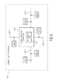
- Fig. 1 is a schematic block diagram of a communication network 100 in accordance with an embodiment of the invention.
- the communication network is configured to facilitate communication among communication devices.
- the communication network 100 includes a transmitter device 102 configured to transmit data and a receiver device configured to receive data 104.
- the data transmitted by the transmitter device and received by the receiver device can be in any suitable format.
- the data transmitted and received are data frames.
- a data frame may include a header segment, a payload segment used to convey application data, and a trailer segment.
- each of the transmitter device and the receiver device may be configured to perform at least one additional function.
- the transmitter device and/or the receiver device may perform an automotive application.
- the transmitter device may also be able to receive signals, for example, from the receiver device.
- the receiver device may also be able to transmit signals, for example, to the transmitter device.
- Signals that are transmitted from the transmitter device 102 can be distorted before being received by the receiver device 104.
- different factors within the communication network 100 can shorten or prolong the length of a transmitted bit. Due to the bit length distortion, the receiver device may not be able to correctly recognize the received bit.
- the receiver device performs an operation for correction of the bit length distortion, which is also referred to as bit reshaping, to reshape shortened and prolonged bits.
- the receiver device 104 includes a bit shaping unit 106 configured to perform bit length correction.
- the bit shaping unit can perform the bit length adjustment using various techniques, such as, oversampling, majority voting, bit strobe and sample counter adjustment.
- the bit shaping unit oversamples digital bits received at the receiver device to generate oversampled bit streams, selects strobing time points that correspond to inner samples in the oversampled bit streams, and outputs the inner samples out of the communication device between the strobing time points.
- An inner sample of an oversampled bit stream is a bit sample that is located between the outer or end samples of the oversampled bit stream.
- an inner sample can be the second bit sample, the third bit sample, or the fourth sample of the bit stream.
- an inner sample can be the second bit sample, the third bit sample, the fourth sample, or the fifth sample of the bit stream.
- an inner sample of an oversampled bit stream is a middle sample where the sample counter is near the half of an oversampling factor.
- the receiver device uses the strobing point based bit reshaping technique, which does not require any additional buffer.
- the transmitter device 102 and the receiver device 104 agree on an oversampling factor and a fixed number of bits between which a synchronization edge (e.g., a rising signal edge or a falling signal edge) is transmitted.
- the receiver device sets a sample counter to one and increments the sample counter every time a new sample is received.
- the receiver device resets the sample counter back to one when the value of the sample counter becomes equal to the oversampling factor or when a synchronization edge is received.
- the value of the sample counter becomes equal to the over sampling factor, which indicates that all samples related to the current bit have been received.
- the sample counter is reset to one such that the first sample of the next bit is properly numbered.
- the sample counter is reset back to one. If there is a deviation between the clocks of the receiver device and transmitter device, the sample counter will not read one at this moment. In this case, the sample counter is reset to align the receiver device to the clock speed of the transmitter device. If there is no deviation between the clocks of the receiver device and the transmitter device, the sample counter will become one at the moment of a transition that marks the beginning of the next bit level.
- Fig. 2 depicts a first embodiment of the bit shaping unit 106.
- a bit shaping unit 206 includes a bit oversampling module 212, a bit majority voting module 214, a strobing point selection module 216, and a bit outputting module 218.
- the bit oversampling module 212 is configured to oversample digital bits received at the receiver device to generate oversampled bit streams with an oversampling factor.
- the bit majority voting module 214 is configured to perform majority voting on each of the oversampled bit streams.
- the bit majority voting module 214 is optional. Thus, in some embodiments, the bit shaping unit 206 does not include the bit majority voting module 214.
- the strobing point selection module 216 is configured to select strobing time points in the oversampled bit streams after the optional majority voting, which correspond to inner samples of the oversampled bit streams with respect to the oversampling factor.
- the bit outputting module 218 is configured to output the inner samples out of the communication device between the strobing time points.
- the bit oversampling module 212 oversamples a bit received at the receiver device 104 to generate an oversampled bit stream and the bit majority voting module 214 performs majority voting on the oversampled bit stream.
- the strobing point selection module 216 selects the current strobing time point from an inner sample in the oversampled bit stream after majority voting and the bit outputting module 218, from the current strobing time point, keeps the inner sample as the output bit of the receiver device until a next strobing time point.
- the next strobing time point can be generated in the same fashion as the current strobing time point, for example, the bit oversampling module 212 oversamples the next bit received at the receiver device to generate the oversampled bit stream and the bit majority voting module 214 performs majority voting on the subsequent oversampled bit stream.
- the strobing time point selection module 216 selects the next strobing time point from an inner sample in the second oversampled bit stream after majority voting.
- Fig. 3 illustrates an example operation of the bit shaping unit 206 depicted in Fig. 2 .
- the example operation includes an oversampling and majority voting process 322 and a bit strobing process 324 that is based on a sample counter.
- the bits from the transmitter device 102 are oversampled at the input of the receiver device 104, e.g., at the bit oversampling module 212, with an oversampling factor.
- the oversampling factor is a positive integer that is typically set to at least 3 or higher.
- one bit can be oversampled with an oversampling factor of 5 to a bit stream having 5 bits.
- the oversampling factor may be known to the transmitter device or even designated by the transmitter device.
- short duration glitches may appear in the oversampled bits. Short duration glitches can cause distortion in the oversampled bits, such as, changing of the value of a bit.
- a majority voting of the oversampled bits may be performed.
- a sliding window consisting of odd number of samples is used for majority voting.
- the value of the majority of the samples within the sliding window is chosen as the output of the bit majority voting unit 214. For example, a sliding window of 3 samples can be used for filtering out in a single erroneous bit.
- majority voting generally cannot cure bit length distortion. Although the majority voted output will be glitch free, the duration of the consecutive bits may still be different from each other.
- a bit strobing technique is used.
- the majority voting does not change the oversampling factor. Consequently, whether the majority voting takes place or not, the strobing point selection module 216 receives as many samples per transmitted bit as the oversampling factor.
- the strobing point selection module 216 strobes the oversampled values at a strobing time point and the bit outputting module 218 keeps outputting that strobed bit value until the next strobing time point. Because a strobed bit value is kept as the output of the receiver device 104 until the next strobing time point, the length of an output bit is the same as the spacing between two consecutive strobing time points.
- the strobing time point is selected such that the strobed bit corresponds to nearly the inner sample with respect to the over sampling factor. Such a strobing time point corresponds to the inner of the eye diagram of the received bits, where a clean signal appears.
- the eye diagram is an oscilloscope display of a digital signal, repetitively sampled to get a good representation of its behavior.
- the strobing time point selection module uses a sample counter, which is set to '1' at the beginning, and increments with the arrival of each oversampled value. At the strobing time point, the received sample becomes the output of the receiver device and is held until the next strobing time point.
- the strobing point selection module 216 selects the oversampled value as the output when the sample counter becomes half (or nearly the half) of the oversampling factor. For example, in an oversampling scheme without an oversampling factor of 8, the strobing point selection module will select the 4 th or the 5 th sample to the output, and the bit outputting module holds the selected sample as output until the next strobing time point. However, in some embodiments, the strobing time point may not be in exactly the middle of the bit stream. For example, for an oversampling factor of 16, the 11 th sample can be chosen as the strobing time point if a cleaner eye opening in the eye diagram is seen slightly after the mid-sample.
- a bit strobing point is selected when the sample counter reaches a particular value, such as around the middle of the oversampling factor.
- the speed of the sample counter depends on the clock of the receiver device 104. Consequently, the spacing period between two consecutive strobing time points depends on the clock of the receiver device.
- the operation described in Fig. 3 is based on the assumption that, when the sample counter becomes half the oversampling factor, the corresponding sample represents the middle of the transmitted bit. However, the assumption only holds when the clocks of both the transmitter device 102 and the receiver device are identical. Typically, clocks of the transmitter device and the receiver device show a certain amount of frequency deviation. To account for the clock deviation, the sample counter of the receiver device needs to be adjusted over time. Fig.
- a bit shaping unit 406 depicted in Fig. 4 includes a strobing point selection module 416, which includes an additional sample clock adjustment module 420 configured to adjust the sample counter.
- the sample clock adjustment module can adjust the sample counter in view of the clock deviation between the transmitter device and the receiver device. For example, the clock deviation between the transmitter device and the receiver device can cause the irregularity of the sample counter and the sample clock adjustment module can adjust the sample counter in view of the irregularity of the sample counter.
- the transmitter device 102 can transmit bits stream having a bit pattern that is known to the receiver device 104 for clock synchronization purpose.
- a synchronization edge e.g., a rising edge or a falling edge
- a known bit edge can be added.
- the sample counter is reset to '1'.
- Fig. 5 illustrates an example operation of the bit shaping unit depicted in Fig. 4 .
- the example operation includes the oversampling and majority voting process 322 and a bit strobing process 524 that is based on sample counter adjustment.
- output bits are generated using the adjusted sample counter.
- the communication network 100 can be used for various applications.
- the communication network 100 is used for an automotive application.
- automotive applications include, without limitation, vehicle dynamics such as braking, suspension, steering, driver assistance, intelligent parking assist, adaptive cruise control, fuel control, traction control, intelligent power assisted steering, lane departure warning, electronic power assisted steering and electronic stability control.
- vehicle dynamics such as braking, suspension, steering, driver assistance, intelligent parking assist, adaptive cruise control, fuel control, traction control, intelligent power assisted steering, lane departure warning, electronic power assisted steering and electronic stability control.
- the communication network 100 facilitates communication among communication devices such as electronic controller nodes in an automobile system, which may be located within a single vehicle or distributed across multiple vehicles.
- Fig. 6 depicts an embodiment of the communication network 100 depicted in Fig. 1 that can be used for an automotive application.
- a communication network 600 includes communication nodes 602-1, 602-2, 602-3, 602-4, 602-5, 602-6 and a central network component 604.
- the communication network 600 is configured to facilitate communication among the communication nodes.
- the communication network 600 is configured to facilitate critical communication (e.g., safety critical communication) among the communication nodes.
- critical communication e.g., safety critical communication
- the communication network 600 is shown in Fig. 6 as including eight communication nodes, in some other embodiments, the communication network 600 includes more than or less than eight communication nodes.
- the communication network 600 is shown in Fig. 6 as including only one central network component, in some other embodiments, the communication network 600 includes multiple central network component.
- the communication nodes 602-1, 602-2, 602-3, 602-4, 602-5, 602-6 of the communication network 600 are configured to transmit and receive data.
- the data transmitted and received by the communication nodes can be in any suitable format.
- the data transmitted and received are data frames.
- each of the communication nodes may be configured to perform an automotive application.
- the communication nodes are electronic controller nodes in an automobile system.
- An electronic controller node contains an electronic control unit (ECU), which may be connected to sensors and actuators. The ECU typically collects data from the sensors, runs application software, controls the actuators, and communicates to other electronic controller nodes via the communication network.
- ECU electronice control unit
- the communication nodes 602-1, 602-2, 602-3, 602-4, 602-5, 602-6 transmit data frames to the buses or branches 608-1, 608-2, 608-3, 608-4 to which they are connected. Likewise, the nodes receive data frames from the bus/branch to which they are connected.
- the central network component 604 may forward a data frame from one branch to one or more destination branches in a number of different ways. For example, the central network component may not forward a data frame to any other branch except one destination branch. The central network component may forward a data frame to multiple branches, such as, to all other branches except the originating branch from which the data frame is received.
- the central network component 604 of the communication network 600 is configured to facilitate critical communication (e.g., safety critical communication) among the communication nodes 602-1, 602-2, 602-3, 602-4, 602-5, 602-6 in the communication network 600.
- the central network component 604 controls communication data transmitted on buses or branches in the communication network 600.
- the central network component 604 selectively blocks and selectively forwards data received on different data transmission buses or branches in the communication network.
- the communication nodes 602-1, 602-2, 602-3, 602-4, 602-5, 602-6 communicate with other nodes exclusively through the central network component 604.
- the central network component 604 may be further configured to store a communication schedule of the communication nodes 602-1, 602-2, 602-3, 602-4, 602-5, 602-6 and configuration parameters.
- the central network component 604 can support a given number of buses in the communication network 600.
- a sub-bus or other communication link/device is connected to a bus in the communication network and communication nodes that perform non-critical applications are connected to the sub-bus or the other communication link/device.
- the central network component 604 is connected to four buses 608-1, 608-2, 608-3, 608-4 in the communication network 600.
- the communication nodes 602-1, 602-2 are connected to the bus 608-1
- the communication node 602-3 is connected to the bus 608-2
- the communication nodes 602-4, 602-5 are connected to the bus 608-3
- the communication node 602-6 is connected to the bus 608-4.
- the four buses are serial communication buses in the communication network.
- the central network component may be a part of an In-Vehicle Network (IVN) system. Although the central network component is shown in Fig. 6 as being connected to four buses, in some other embodiments, the central network component is connected to more than or less than four buses.
- IVN In-Vehicle Network
- At least one of the communication nodes 602-1, 602-2, 602-3, 602-4, 602-5, 602-6 is directly connected to a bus in the communication network.
- at least one of the communication nodes is connected to a bus in the communication network 600 without any intermediate device.
- the robustness of safety critical communication of an application system can be improved by connecting communication nodes in the application system to the central network component 604.
- the central network component 604 can block unwanted communication in the automobile system and protect the safety critical communication.
- the communication nodes 602-1, 602-2, 602-3, 602-4, 602-5, 602-6 are possible implementations of the transmitter device 102. However, the transmitter device can be implemented differently from the communication nodes depicted in Fig. 6 .
- the central network component 604 is one of possible implementations of the receiver device 104. However, the receiver device can be implemented differently from the central network component depicted in Fig. 6 .
- the invention is not restricted to the particular implementation of the communication nodes and the central network component depicted in Fig. 6 .
- all of the communication nodes 602-1, 602-2, 602-3, 602-4, 602-5, 602-6 are communication nodes of a FlexRayTM communication system in accordance to the FlexRayTM communication system specifications developed by the FlexRayTM Consortium.
- a FlexRayTM communication system is a robust, scalable, deterministic and fault-tolerant digital serial bus system for automotive applications.
- a FlexRayTM communication system can be used by a car manufacturer to adopt an in-vehicle network (IVN) with high data communication speeds to accommodate advanced features in automobiles.
- the central network component 604 is connected to a channel of the FlexRayTM communication system to enable data transfer on the channel and to increase fault tolerance.
- a channel of the FlexRayTM communication system is a single communication medium, e.g., one network.
- the FlexRayTM communication system specifications distinguish between two independent, parallel communication media, a channel A and a channel B.
- the central network component 604 may be implemented as a FlexRay-compatible central network component, such as a FlexRay-compatible switch or a FlexRay-compatible central bus guardian (CBG), which is designed, developed, manufactured, and/or configured compatibly with or in accordance to the FlexRayTM communication system specifications developed by the FlexRayTM Consortium.
- CBG central bus guardian
- central network component When the central network component is used to protect a channel of a FlexRayTM communication system, some critical faults (e.g., short circuited bus lines or erroneous behavior of a communication node) can be tolerated by the FlexRayTM communication system.
- multiple central network components are cascaded on one channel of a FlexRayTM communication system. For example, if a single central network component is not connected to a sufficient number of buses/branches for a certain FlexRayTM communication system, multiple central network component can be cascaded on one channel of the FlexRayTM communication system such that a sufficient number of buses are provided.
- Different factors within the communication network 600 can shorten or prolong the length of a transmitted bit. Due to the bit length distortion, a receiving communication node 602-1, 602-2, 602-3, 602-4, 602-5, or 602-6 may not be able to recognize the received bits correctly. If the central network component 604 forwards the distorted bit stream to other buses/branches 608-1, 608-2, 608-3, 608-4 of the communication network 600, interferences may cause more distortions and the nodes on the other buses/branches may not be able to recognize the bit stream correctly. The central network component can reshape the received bits from the communication nodes 602-1, 602-2, 602-3, 602-4, 602-5, 602-6 before forwarding them to other network nodes.
- the central network component includes a bit shaping unit 606, which is the same as or similar to the bit shaping units 106, 206, 406 depicted in Figs. 1 , 2 and 4 .
- the bit shaping unit 606 can shorten and prolong bits based on bit strobing with edge based sample counter adjustment. Consequently, the signal quality on different buses 608-1, 608-2, 608-3, 608-4 and more reliable communication between the communication nodes 602-1, 602-2, 602-3, 602-4, 602-5, 602-6 can be ensured.
- Figs. 7 and 8 show some examples of transmitted bits, sample counter values, voted bit samples and strobed output bits in the communication network 600.
- the oversampling factor is 8.
- a communication node 602-1, 602-2, 602-3, 602-4, 602-5, or 602-6 sends a '0,' followed by a '1,' to the central network component 604. If there is no bit length distortion, the central network component will sample 8 zeros, followed by 8 ones. However, due to disturbances, the length of the received bit samples may change.
- Fig. 7 shows some examples of transmitted bits, sample counter values, voted bit samples and strobed output bits in the communication network 600.
- the oversampling factor is 8.
- a communication node 602-1, 602-2, 602-3, 602-4, 602-5, or 602-6 sends a '0,' followed by a '1,' to the central network component 604. If there is no bit length distortion, the central network component will sample 8 zeros, followed by 8 ones. However,
- the oversampled bit stream of the first bit, '0,' has 10 bits and the oversampled bit stream of the second bit, '1,' has 6 bits.
- Short duration glitches may cause a '1' in between the run of zeros, and a '0' in between the run of ones.
- a majority voting with a sliding window of 5 samples can remove such glitches.
- a bit strobing time point is selected from the voted samples. Because the input is oversampled 8 times, the 5 th bit of each bit stream can be selected as the bit strobing time point and is outputted out of the central network component. In some embodiments, instead of the 5th bit of each bit stream, the 4th bit of each bit stream is selected as the bit strobing time point. Consequently, the length of each output bit becomes equal, which are 8 sample clocks of the central network component.
- the bit strobing introduces delay into the relaying of the received bits.
- the delay, "dl,” due to the strobing technique is equal to 4 sample clocks.
- additional delays can be incurred due to the majority voting and sample register at the input.
- the total digital delay for the relaying of the received bits is equal to the sum of the input sample register delay, the majority voting delay and the strobing delay. For a majority voting between 5 samples, the voting delay is 3 sample clocks.
- the total digital delay is 8 (i.e., 1+3+4) sample clocks.
- a communication node 602-1, 602-2, 602-3, 602-4, 602-5, or 602-6 sends a Byte Start Sequence (BSS) that includes a HIGH bit, '1,' followed by a LOW bit, '0,' to the central network component 604.
- BSS Byte Start Sequence
- the FlexRay protocol uses a Byte Start Sequence (BSS) at the beginning of each byte.
- the falling edge of the BSS which is the transition from HIGH bit to LOW bit, is used as the synchronization edge. If there is no bit length distortion, the sample counter of the will read 8, which is the oversampling factor, when the last sample of the HIGH bit is received.
- the sample counter is reset to 1 and the central network component takes the first sample of the LOW bit. If the transmitting communication node has a faster clock than the central network component, the sample counter will read less than 8 when the last sample of the HIGH bit is received. In the example shown in Fig. 8 , the sample counter reads 7 when the last sample of the HIGH bit is received. When the edge is received, the sample counter becomes 8. Because the central network component is aware of the synchronization edge, the central network component resets the sample counter to 1. The central network component adjusts the sample counter so that it becomes 2 with the arrival of the next voted sample.
- the 5th bit of each bit stream can be selected as the bit strobing time point and is outputted out of the central network component, which causes the first bit of the BSS to have a shorter duration of 7 samples, instead of the nominal 8 samples.
- the 4th bit of each bit stream is selected as the bit strobing time point.
- Fig. 9 is a process flow diagram of a method for bit processing in a central network component for facilitating communication among communication nodes in accordance with an embodiment of the invention.
- the central network component may be similar to or same as the central network component 604 depicted in Fig. 6 .
- bits received at the central network component from a first communication node of the communication nodes are oversampled with an oversampling factor to generate oversampled bit streams.
- time points are selected in the oversampled bit streams, where the time points correspond to inner samples of the oversampled bit streams with respect to the oversampling factor.
- the inner samples are outputted out of the central network component to a second communication node of the communication nodes between the time points.
- the various components or units of the embodiments that have been described or depicted may be implemented in hardware, software that is stored in a non-transitory computer readable medium or a combination of hardware and software that is stored in a non-transitory computer readable medium.
- the non-transitory computer readable medium can be an electronic, magnetic, optical, electromagnetic, infrared, or semiconductor system (or apparatus or device), or a propagation medium. Examples of a non-transitory computer-readable medium include a semiconductor or solid state memory, magnetic tape, a removable computer diskette, a random access memory (RAM), a read-only memory (ROM), a rigid magnetic disk, and an optical disk.
- optical disks include a compact disk with read only memory (CD-ROM), a compact disk with read/write (CD-R/W), a digital video disk (DVD), and a Blu-ray disk.
- CD-ROM compact disk with read only memory
- CD-R/W compact disk with read/write
- DVD digital video disk
- Blu-ray disk a Blu-ray disk.
- the various components or units of the embodiments e.g., the bit shaping unit 106, 206, 406, or 606
- a processor may include a multifunction processor and/or an application-specific processor.
Landscapes
- Engineering & Computer Science (AREA)
- Computer Networks & Wireless Communication (AREA)
- Signal Processing (AREA)
- Small-Scale Networks (AREA)
Abstract
Description
- Embodiments of the invention relate generally to processing systems and methods and, more particularly, to systems and methods for bit processing for a central network component.
- Communication devices in an application system can communicate with each other directly or through a communication hub device. Signals that are transmitted from a transmitter device can be distorted before being received by a receiver device. Shortening or prolonging of the length of a transmitted bit is referred to as a bit length distortion. The bit length distortion may be caused by static delays due to, such as, topology or terminators, or stochastic delays due to, such as, Electromagnetic interference (EMI) or clock jitters. Because of the bit length distortion, the receiver device may not be able to correctly recognize the received bit. To deal with the bit length distortion, the receiver device typically performs some form of bit length correction. The situation gets even worse when the transmitter and receiver nodes are connected via a central network component and the central component forwards the distorted bit stream from the transmitter to the receiver. Further interferences in the link between the central component and the receiver may cause more distortions and the receiver may not be able to recover the received bit stream correctly.
- Conventionally, a buffer, such as a First In First Out (FIFO) buffer, is used in a central component for bit length correction purpose. For example, a buffer can be added between a decoder and a subsequent encoder to temporarily store data (e.g., data bits) that is transferred from the decoder to the encoder. Saving the decoded bits in the buffer allows the decoded bits to be correctly encoded and transmitted to other devices. However, having such a buffer introduces a delay in the signal path. Typically, a time budget is allocated for the bit processing of a central component. The delay introduced by the buffer may cause the total delay in the central component to exceed the time budget. In addition to the delay, the added buffer also increases the silicon area of the receiver device. For example, if a central component has to allow simultaneous communication in parallel, it needs a buffer for each parallel communication. However, having multiple buffers increases the silicon area.
- A central network component, a FlexRay-compatible central network component, and a method for bit processing in a central network component are described. In one embodiment, a central network component for facilitating communication among communication nodes includes a bit oversampling module configured to oversample bits received from a first communication node of the communication nodes with an oversampling factor to generate oversampled bit streams, a time point selection module configured to select time points in the oversampled bit streams, where the time points correspond to inner samples of the oversampled bit streams with respect to the oversampling factor, and a bit outputting module configured to output the inner samples to a second communication node of the communication nodes between the time points. Other embodiments are also described.
- In one embodiment, a FlexRay-compatible central network component for facilitating communication among FlexRay-compatible communication nodes in an automobile system includes a bit processing unit comprising: a bit oversampling module configured to oversample bits received from a first FlexRay-compatible communication node of the FlexRay-compatible communication nodes with an oversampling factor to generate oversampled bit streams, a time point selection module configured to select time points in the oversampled bit streams, where the time points correspond to inner samples of the oversampled bit streams with respect to the oversampling factor, and a bit outputting module configured to output the inner samples to a second FlexRay-compatible communication node of the FlexRay-compatible communication nodes between the time points.
- In one embodiment, a method for bit processing in a central network component for facilitating communication among communication nodes involves oversampling bits received at the central network component from a first communication node of the communication nodes with an oversampling factor to generate oversampled bit streams, selecting time points in the oversampled bit streams, where the time points correspond to inner samples of the oversampled bit streams with respect to the oversampling factor, and outputting the inner samples out of the central network component to a second communication node of the communication nodes between the time points.
- Other aspects and advantages of embodiments of the present invention will become apparent from the following detailed description, taken in conjunction with the accompanying drawings, depicted by way of example of the principles of the invention.
-
Fig. 1 is a schematic block diagram of a communication network in accordance with an embodiment of the invention. -
Fig. 2 depicts a first embodiment of a bit shaping unit of a receiver device of the communication network depicted inFig. 1 . -
Fig. 3 illustrates an example operation of the bit shaping unit depicted inFig. 2 . -
Fig. 4 depicts a second embodiment of the bit shaping unit of the receiver device of the communication network depicted inFig. 1 . -
Fig. 5 illustrates an example operation of the bit shaping unit depicted inFig. 4 . -
Fig. 6 depicts an embodiment of the communication network depicted inFig. 1 that can be used for an automotive application. -
Figs. 7 and8 show some examples of transmitted bits, sample counter values, voted bit samples and output bits in the communication network depicted inFig. 6 . -
Fig. 9 is a process flow diagram of a method for bit processing in a communication device in accordance with an embodiment of the invention. - Throughout the description, similar reference numbers may be used to identify similar elements.
- It will be readily understood that the components of the embodiments as generally described herein and illustrated in the appended figures could be arranged and designed in a wide variety of different configurations. Thus, the following detailed description of various embodiments, as represented in the figures, is not intended to limit the scope of the present disclosure, but is merely representative of various embodiments. While the various aspects of the embodiments are presented in drawings, the drawings are not necessarily drawn to scale unless specifically indicated.
- The described embodiments are to be considered in all respects only as illustrative and not restrictive. The scope of the invention is, therefore, indicated by the appended claims rather than by this detailed description. All changes which come within the meaning and range of equivalency of the claims are to be embraced within their scope.
- Reference throughout this specification to features, advantages, or similar language does not imply that all of the features and advantages that may be realized with the present invention should be or are in any single embodiment. Rather, language referring to the features and advantages is understood to mean that a specific feature, advantage, or characteristic described in connection with an embodiment is included in at least one embodiment. Thus, discussions of the features and advantages, and similar language, throughout this specification may, but do not necessarily, refer to the same embodiment.
- Furthermore, the described features, advantages, and characteristics of the invention may be combined in any suitable manner in one or more embodiments. One skilled in the relevant art will recognize, in light of the description herein, that the invention can be practiced without one or more of the specific features or advantages of a particular embodiment. In other instances, additional features and advantages may be recognized in certain embodiments that may not be present in all embodiments of the invention.
- Reference throughout this specification to "one embodiment," "an embodiment," or similar language means that a particular feature, structure, or characteristic described in connection with the indicated embodiment is included in at least one embodiment. Thus, the phrases "in one embodiment," "in an embodiment," and similar language throughout this specification may, but do not necessarily, all refer to the same embodiment.
-
Fig. 1 is a schematic block diagram of acommunication network 100 in accordance with an embodiment of the invention. The communication network is configured to facilitate communication among communication devices. In the embodiment depicted inFig. 1 , thecommunication network 100 includes atransmitter device 102 configured to transmit data and a receiver device configured to receivedata 104. The data transmitted by the transmitter device and received by the receiver device can be in any suitable format. In an embodiment, the data transmitted and received are data frames. A data frame may include a header segment, a payload segment used to convey application data, and a trailer segment. In addition to communication, each of the transmitter device and the receiver device may be configured to perform at least one additional function. For example, the transmitter device and/or the receiver device may perform an automotive application. The transmitter device may also be able to receive signals, for example, from the receiver device. The receiver device may also be able to transmit signals, for example, to the transmitter device. - Signals that are transmitted from the
transmitter device 102 can be distorted before being received by thereceiver device 104. For example, different factors within thecommunication network 100 can shorten or prolong the length of a transmitted bit. Due to the bit length distortion, the receiver device may not be able to correctly recognize the received bit. To tackle the bit length distortion, the receiver device performs an operation for correction of the bit length distortion, which is also referred to as bit reshaping, to reshape shortened and prolonged bits. - In the embodiment depicted in
Fig. 1 , thereceiver device 104 includes abit shaping unit 106 configured to perform bit length correction. The bit shaping unit can perform the bit length adjustment using various techniques, such as, oversampling, majority voting, bit strobe and sample counter adjustment. In an embodiment, the bit shaping unit oversamples digital bits received at the receiver device to generate oversampled bit streams, selects strobing time points that correspond to inner samples in the oversampled bit streams, and outputs the inner samples out of the communication device between the strobing time points. An inner sample of an oversampled bit stream is a bit sample that is located between the outer or end samples of the oversampled bit stream. For example, for a bit stream that has five bit samples, an inner sample can be the second bit sample, the third bit sample, or the fourth sample of the bit stream. In another example, for a bit stream that has six bit samples, an inner sample can be the second bit sample, the third bit sample, the fourth sample, or the fifth sample of the bit stream. In some embodiment, an inner sample of an oversampled bit stream is a middle sample where the sample counter is near the half of an oversampling factor. The receiver device uses the strobing point based bit reshaping technique, which does not require any additional buffer. - In an exemplary operation of the
communication network 100, thetransmitter device 102 and thereceiver device 104 agree on an oversampling factor and a fixed number of bits between which a synchronization edge (e.g., a rising signal edge or a falling signal edge) is transmitted. The receiver device sets a sample counter to one and increments the sample counter every time a new sample is received. The receiver device resets the sample counter back to one when the value of the sample counter becomes equal to the oversampling factor or when a synchronization edge is received. Specifically, when the number of samples received becomes equal to the over sampling factor, the value of the sample counter becomes equal to the over sampling factor, which indicates that all samples related to the current bit have been received. Consequently, the sample counter is reset to one such that the first sample of the next bit is properly numbered. When a synchronization edge is received, the sample counter is reset back to one. If there is a deviation between the clocks of the receiver device and transmitter device, the sample counter will not read one at this moment. In this case, the sample counter is reset to align the receiver device to the clock speed of the transmitter device. If there is no deviation between the clocks of the receiver device and the transmitter device, the sample counter will become one at the moment of a transition that marks the beginning of the next bit level. - Two embodiments of the
bit shaping unit 106 are described with respect toFigs. 2-5 .Fig. 2 depicts a first embodiment of thebit shaping unit 106. In the embodiment depicted inFig. 2 , abit shaping unit 206 includes abit oversampling module 212, a bitmajority voting module 214, a strobingpoint selection module 216, and abit outputting module 218. - The
bit oversampling module 212 is configured to oversample digital bits received at the receiver device to generate oversampled bit streams with an oversampling factor. The bitmajority voting module 214 is configured to perform majority voting on each of the oversampled bit streams. The bitmajority voting module 214 is optional. Thus, in some embodiments, thebit shaping unit 206 does not include the bitmajority voting module 214. The strobingpoint selection module 216 is configured to select strobing time points in the oversampled bit streams after the optional majority voting, which correspond to inner samples of the oversampled bit streams with respect to the oversampling factor. Thebit outputting module 218 is configured to output the inner samples out of the communication device between the strobing time points. - In an embodiment, the
bit oversampling module 212 oversamples a bit received at thereceiver device 104 to generate an oversampled bit stream and the bitmajority voting module 214 performs majority voting on the oversampled bit stream. The strobingpoint selection module 216 selects the current strobing time point from an inner sample in the oversampled bit stream after majority voting and thebit outputting module 218, from the current strobing time point, keeps the inner sample as the output bit of the receiver device until a next strobing time point. The next strobing time point can be generated in the same fashion as the current strobing time point, for example, thebit oversampling module 212 oversamples the next bit received at the receiver device to generate the oversampled bit stream and the bitmajority voting module 214 performs majority voting on the subsequent oversampled bit stream. The strobing timepoint selection module 216 selects the next strobing time point from an inner sample in the second oversampled bit stream after majority voting. -
Fig. 3 illustrates an example operation of thebit shaping unit 206 depicted inFig. 2 . In the embodiment depicted inFig. 3 , the example operation includes an oversampling andmajority voting process 322 and abit strobing process 324 that is based on a sample counter. The bits from thetransmitter device 102 are oversampled at the input of thereceiver device 104, e.g., at thebit oversampling module 212, with an oversampling factor. For example, a single bit is oversampled to a bit stream and the number of bits in the bit stream is equal to the oversampling factor. The oversampling factor is a positive integer that is typically set to at least 3 or higher. For example, one bit can be oversampled with an oversampling factor of 5 to a bit stream having 5 bits. The oversampling factor may be known to the transmitter device or even designated by the transmitter device. - In some cases, short duration glitches may appear in the oversampled bits. Short duration glitches can cause distortion in the oversampled bits, such as, changing of the value of a bit. To remove short duration glitches, a majority voting of the oversampled bits may be performed. In an embodiment, a sliding window consisting of odd number of samples is used for majority voting. In this embodiment, the value of the majority of the samples within the sliding window is chosen as the output of the bit
majority voting unit 214. For example, a sliding window of 3 samples can be used for filtering out in a single erroneous bit. However, majority voting generally cannot cure bit length distortion. Although the majority voted output will be glitch free, the duration of the consecutive bits may still be different from each other. - To reshape the bit length, a bit strobing technique is used. The majority voting does not change the oversampling factor. Consequently, whether the majority voting takes place or not, the strobing
point selection module 216 receives as many samples per transmitted bit as the oversampling factor. The strobingpoint selection module 216 strobes the oversampled values at a strobing time point and thebit outputting module 218 keeps outputting that strobed bit value until the next strobing time point. Because a strobed bit value is kept as the output of thereceiver device 104 until the next strobing time point, the length of an output bit is the same as the spacing between two consecutive strobing time points. The strobing time point is selected such that the strobed bit corresponds to nearly the inner sample with respect to the over sampling factor. Such a strobing time point corresponds to the inner of the eye diagram of the received bits, where a clean signal appears. The eye diagram is an oscilloscope display of a digital signal, repetitively sampled to get a good representation of its behavior. In an embodiment, the strobing time point selection module uses a sample counter, which is set to '1' at the beginning, and increments with the arrival of each oversampled value. At the strobing time point, the received sample becomes the output of the receiver device and is held until the next strobing time point. The strobingpoint selection module 216 selects the oversampled value as the output when the sample counter becomes half (or nearly the half) of the oversampling factor. For example, in an oversampling scheme without an oversampling factor of 8, the strobing point selection module will select the 4th or the 5th sample to the output, and the bit outputting module holds the selected sample as output until the next strobing time point. However, in some embodiments, the strobing time point may not be in exactly the middle of the bit stream. For example, for an oversampling factor of 16, the 11th sample can be chosen as the strobing time point if a cleaner eye opening in the eye diagram is seen slightly after the mid-sample. - A bit strobing point is selected when the sample counter reaches a particular value, such as around the middle of the oversampling factor. The speed of the sample counter depends on the clock of the
receiver device 104. Consequently, the spacing period between two consecutive strobing time points depends on the clock of the receiver device. The operation described inFig. 3 is based on the assumption that, when the sample counter becomes half the oversampling factor, the corresponding sample represents the middle of the transmitted bit. However, the assumption only holds when the clocks of both thetransmitter device 102 and the receiver device are identical. Typically, clocks of the transmitter device and the receiver device show a certain amount of frequency deviation. To account for the clock deviation, the sample counter of the receiver device needs to be adjusted over time.Fig. 4 depicts a second embodiment of thebit shaping unit 106 that can adjust the sample counter. Compared to thebit shaping unit 206 depicted inFig. 2 , abit shaping unit 406 depicted inFig. 4 includes a strobingpoint selection module 416, which includes an additional sampleclock adjustment module 420 configured to adjust the sample counter. The sample clock adjustment module can adjust the sample counter in view of the clock deviation between the transmitter device and the receiver device. For example, the clock deviation between the transmitter device and the receiver device can cause the irregularity of the sample counter and the sample clock adjustment module can adjust the sample counter in view of the irregularity of the sample counter. - The
transmitter device 102 can transmit bits stream having a bit pattern that is known to thereceiver device 104 for clock synchronization purpose. In an embodiment, a synchronization edge (e.g., a rising edge or a falling edge) is transmitted between a fixed number of bits. For example, at the beginning of each transmitted byte or a number of transmitted bytes, a known bit edge can be added. When the known bit edge is received, the sample counter is reset to '1'.Fig. 5 illustrates an example operation of the bit shaping unit depicted inFig. 4 . In the embodiment depicted inFig. 5 , the example operation includes the oversampling andmajority voting process 322 and abit strobing process 524 that is based on sample counter adjustment. Compared to the example operation described with reference toFig. 3 , in the example operation illustrated inFig. 5 , output bits are generated using the adjusted sample counter. - Turning back to
Fig. 1 , thecommunication network 100 can be used for various applications. In an embodiment, thecommunication network 100 is used for an automotive application. Examples of automotive applications include, without limitation, vehicle dynamics such as braking, suspension, steering, driver assistance, intelligent parking assist, adaptive cruise control, fuel control, traction control, intelligent power assisted steering, lane departure warning, electronic power assisted steering and electronic stability control. For example, thecommunication network 100 facilitates communication among communication devices such as electronic controller nodes in an automobile system, which may be located within a single vehicle or distributed across multiple vehicles. -
Fig. 6 depicts an embodiment of thecommunication network 100 depicted inFig. 1 that can be used for an automotive application. In the embodiment depicted inFig. 6 , acommunication network 600 includes communication nodes 602-1, 602-2, 602-3, 602-4, 602-5, 602-6 and acentral network component 604. Thecommunication network 600 is configured to facilitate communication among the communication nodes. In an embodiment, thecommunication network 600 is configured to facilitate critical communication (e.g., safety critical communication) among the communication nodes. Although thecommunication network 600 is shown inFig. 6 as including eight communication nodes, in some other embodiments, thecommunication network 600 includes more than or less than eight communication nodes. Although thecommunication network 600 is shown inFig. 6 as including only one central network component, in some other embodiments, thecommunication network 600 includes multiple central network component. - The communication nodes 602-1, 602-2, 602-3, 602-4, 602-5, 602-6 of the
communication network 600 are configured to transmit and receive data. The data transmitted and received by the communication nodes can be in any suitable format. In an embodiment, the data transmitted and received are data frames. In addition to communication, each of the communication nodes may be configured to perform an automotive application. In an embodiment, the communication nodes are electronic controller nodes in an automobile system. An electronic controller node contains an electronic control unit (ECU), which may be connected to sensors and actuators. The ECU typically collects data from the sensors, runs application software, controls the actuators, and communicates to other electronic controller nodes via the communication network. - The communication nodes 602-1, 602-2, 602-3, 602-4, 602-5, 602-6 transmit data frames to the buses or branches 608-1, 608-2, 608-3, 608-4 to which they are connected. Likewise, the nodes receive data frames from the bus/branch to which they are connected. The
central network component 604 may forward a data frame from one branch to one or more destination branches in a number of different ways. For example, the central network component may not forward a data frame to any other branch except one destination branch. The central network component may forward a data frame to multiple branches, such as, to all other branches except the originating branch from which the data frame is received. Thecentral network component 604 of thecommunication network 600 is configured to facilitate critical communication (e.g., safety critical communication) among the communication nodes 602-1, 602-2, 602-3, 602-4, 602-5, 602-6 in thecommunication network 600. For example, thecentral network component 604 controls communication data transmitted on buses or branches in thecommunication network 600. In an embodiment, thecentral network component 604 selectively blocks and selectively forwards data received on different data transmission buses or branches in the communication network. In some embodiments, the communication nodes 602-1, 602-2, 602-3, 602-4, 602-5, 602-6 communicate with other nodes exclusively through thecentral network component 604. Thecentral network component 604 may be further configured to store a communication schedule of the communication nodes 602-1, 602-2, 602-3, 602-4, 602-5, 602-6 and configuration parameters. Thecentral network component 604 can support a given number of buses in thecommunication network 600. In an embodiment, a sub-bus or other communication link/device is connected to a bus in the communication network and communication nodes that perform non-critical applications are connected to the sub-bus or the other communication link/device. In the embodiment depicted inFig. 6 , thecentral network component 604 is connected to four buses 608-1, 608-2, 608-3, 608-4 in thecommunication network 600. Specifically, the communication nodes 602-1, 602-2 are connected to the bus 608-1, the communication node 602-3 is connected to the bus 608-2, the communication nodes 602-4, 602-5 are connected to the bus 608-3, the communication node 602-6 is connected to the bus 608-4. In an embodiment, the four buses are serial communication buses in the communication network. The central network component may be a part of an In-Vehicle Network (IVN) system. Although the central network component is shown inFig. 6 as being connected to four buses, in some other embodiments, the central network component is connected to more than or less than four buses. In an embodiment, at least one of the communication nodes 602-1, 602-2, 602-3, 602-4, 602-5, 602-6 is directly connected to a bus in the communication network. In other words, at least one of the communication nodes is connected to a bus in thecommunication network 600 without any intermediate device. In an embodiment, the robustness of safety critical communication of an application system such as an automobile system can be improved by connecting communication nodes in the application system to thecentral network component 604. For example, thecentral network component 604 can block unwanted communication in the automobile system and protect the safety critical communication. - The communication nodes 602-1, 602-2, 602-3, 602-4, 602-5, 602-6 are possible implementations of the
transmitter device 102. However, the transmitter device can be implemented differently from the communication nodes depicted inFig. 6 . In addition, thecentral network component 604 is one of possible implementations of thereceiver device 104. However, the receiver device can be implemented differently from the central network component depicted inFig. 6 . The invention is not restricted to the particular implementation of the communication nodes and the central network component depicted inFig. 6 . - In an embodiment, all of the communication nodes 602-1, 602-2, 602-3, 602-4, 602-5, 602-6 are communication nodes of a FlexRay™ communication system in accordance to the FlexRay™ communication system specifications developed by the FlexRay™ Consortium. A FlexRay™ communication system is a robust, scalable, deterministic and fault-tolerant digital serial bus system for automotive applications. For example, a FlexRay™ communication system can be used by a car manufacturer to adopt an in-vehicle network (IVN) with high data communication speeds to accommodate advanced features in automobiles. In this embodiment, the
central network component 604 is connected to a channel of the FlexRay™ communication system to enable data transfer on the channel and to increase fault tolerance. A channel of the FlexRay™ communication system is a single communication medium, e.g., one network. For example, the FlexRay™ communication system specifications distinguish between two independent, parallel communication media, a channel A and a channel B. Thecentral network component 604 may be implemented as a FlexRay-compatible central network component, such as a FlexRay-compatible switch or a FlexRay-compatible central bus guardian (CBG), which is designed, developed, manufactured, and/or configured compatibly with or in accordance to the FlexRay™ communication system specifications developed by the FlexRay™ Consortium. When the central network component is used to protect a channel of a FlexRay™ communication system, some critical faults (e.g., short circuited bus lines or erroneous behavior of a communication node) can be tolerated by the FlexRay™ communication system. In an embodiment, multiple central network components are cascaded on one channel of a FlexRay™ communication system. For example, if a single central network component is not connected to a sufficient number of buses/branches for a certain FlexRay™ communication system, multiple central network component can be cascaded on one channel of the FlexRay™ communication system such that a sufficient number of buses are provided. - Different factors within the
communication network 600 can shorten or prolong the length of a transmitted bit. Due to the bit length distortion, a receiving communication node 602-1, 602-2, 602-3, 602-4, 602-5, or 602-6 may not be able to recognize the received bits correctly. If thecentral network component 604 forwards the distorted bit stream to other buses/branches 608-1, 608-2, 608-3, 608-4 of thecommunication network 600, interferences may cause more distortions and the nodes on the other buses/branches may not be able to recognize the bit stream correctly. The central network component can reshape the received bits from the communication nodes 602-1, 602-2, 602-3, 602-4, 602-5, 602-6 before forwarding them to other network nodes. In the embodiment depicted inFig. 6 , the central network component includes abit shaping unit 606, which is the same as or similar to thebit shaping units Figs. 1 ,2 and4 . Thebit shaping unit 606 can shorten and prolong bits based on bit strobing with edge based sample counter adjustment. Consequently, the signal quality on different buses 608-1, 608-2, 608-3, 608-4 and more reliable communication between the communication nodes 602-1, 602-2, 602-3, 602-4, 602-5, 602-6 can be ensured. -
Figs. 7 and8 show some examples of transmitted bits, sample counter values, voted bit samples and strobed output bits in thecommunication network 600. In the examples shown inFigs. 7 and8 , the oversampling factor is 8. In the example shown inFig. 7 , a communication node 602-1, 602-2, 602-3, 602-4, 602-5, or 602-6 sends a '0,' followed by a '1,' to thecentral network component 604. If there is no bit length distortion, the central network component will sample 8 zeros, followed by 8 ones. However, due to disturbances, the length of the received bit samples may change. In the example shown inFig. 7 , the oversampled bit stream of the first bit, '0,' has 10 bits and the oversampled bit stream of the second bit, '1,' has 6 bits. Short duration glitches may cause a '1' in between the run of zeros, and a '0' in between the run of ones. However, a majority voting with a sliding window of 5 samples can remove such glitches. A bit strobing time point is selected from the voted samples. Because the input is oversampled 8 times, the 5th bit of each bit stream can be selected as the bit strobing time point and is outputted out of the central network component. In some embodiments, instead of the 5th bit of each bit stream, the 4th bit of each bit stream is selected as the bit strobing time point. Consequently, the length of each output bit becomes equal, which are 8 sample clocks of the central network component. - The bit strobing introduces delay into the relaying of the received bits. In the example shown in
Fig. 7 , the delay, "dl," due to the strobing technique is equal to 4 sample clocks. In addition to the delay introduced by the bit strobing, additional delays can be incurred due to the majority voting and sample register at the input. The total digital delay for the relaying of the received bits is equal to the sum of the input sample register delay, the majority voting delay and the strobing delay. For a majority voting between 5 samples, the voting delay is 3 sample clocks. When the input sample register introduces a delay of 1 sample clock, the total digital delay is 8 (i.e., 1+3+4) sample clocks. - In the example shown in
Fig. 8 , a communication node 602-1, 602-2, 602-3, 602-4, 602-5, or 602-6 sends a Byte Start Sequence (BSS) that includes a HIGH bit, '1,' followed by a LOW bit, '0,' to thecentral network component 604. For example, the FlexRay protocol uses a Byte Start Sequence (BSS) at the beginning of each byte. The falling edge of the BSS, which is the transition from HIGH bit to LOW bit, is used as the synchronization edge. If there is no bit length distortion, the sample counter of the will read 8, which is the oversampling factor, when the last sample of the HIGH bit is received. Afterward, the sample counter is reset to 1 and the central network component takes the first sample of the LOW bit. If the transmitting communication node has a faster clock than the central network component, the sample counter will read less than 8 when the last sample of the HIGH bit is received. In the example shown inFig. 8 , the sample counter reads 7 when the last sample of the HIGH bit is received. When the edge is received, the sample counter becomes 8. Because the central network component is aware of the synchronization edge, the central network component resets the sample counter to 1. The central network component adjusts the sample counter so that it becomes 2 with the arrival of the next voted sample. Because the input is oversampled 8 times, the 5th bit of each bit stream can be selected as the bit strobing time point and is outputted out of the central network component, which causes the first bit of the BSS to have a shorter duration of 7 samples, instead of the nominal 8 samples. In some embodiments, instead of the 5th bit of each bit stream, the 4th bit of each bit stream is selected as the bit strobing time point. -
Fig. 9 is a process flow diagram of a method for bit processing in a central network component for facilitating communication among communication nodes in accordance with an embodiment of the invention. The central network component may be similar to or same as thecentral network component 604 depicted inFig. 6 . Atblock 902, bits received at the central network component from a first communication node of the communication nodes are oversampled with an oversampling factor to generate oversampled bit streams. Atblock 904, time points are selected in the oversampled bit streams, where the time points correspond to inner samples of the oversampled bit streams with respect to the oversampling factor. Atblock 906, the inner samples are outputted out of the central network component to a second communication node of the communication nodes between the time points. - The various components or units of the embodiments that have been described or depicted (e.g., the
bit shaping unit bit shaping unit - Although the operations of the method herein are shown and described in a particular order, the order of the operations of the method may be altered so that certain operations may be performed in an inverse order or so that certain operations may be performed, at least in part, concurrently with other operations. In another embodiment, instructions or sub-operations of distinct operations may be implemented in an intermittent and/or alternating manner.
- In addition, although specific embodiments of the invention that have been described or depicted include several components described or depicted herein, other embodiments of the invention may include fewer or more components to implement less or more feature.
- Furthermore, although specific embodiments of the invention have been described and depicted, the invention is not to be limited to the specific forms or arrangements of parts so described and depicted. The scope of the invention is to be defined by the claims appended hereto and their equivalents.
Claims (15)
- A central network component for facilitating communication among communication nodes, the central network component comprising:a bit oversampling module configured to oversample a plurality of bits received from a first communication node of the communication nodes with an oversampling factor to generate oversampled bit streams;a time point selection module configured to select time points in the oversampled bit streams, wherein the time points correspond to inner samples of the oversampled bit streams with respect to the oversampling factor; anda bit outputting module configured to output the inner samples to a second communication node of the communication nodes between the time points.
- The central network component of claim 1, wherein the bit outputting module is further configured to output one of the inner samples out of the central network component between a corresponding time point of the time points and a subsequent time point of the time points, or
wherein the bit outputting module is further configured to, from one of the time points, keep a corresponding one of the inner samples as the output bit of the central network component until a next time point. - The central network component of claim 1, wherein the time point selection module is further configured to:increase a sample counter for each bit in one of the oversampled bit streams; andselect a time point in the one of the oversampled bit streams when the sample counter is around a half of the oversampling factor.
- The central network component of claim 1, wherein the bit oversampling module is further configured to oversample a first received bit to generate a first oversampled bit stream and oversample a second received bit to generate a second oversampled bit stream, wherein the time point selection module is further configured to select a first time point that corresponds to an inner sample in the first oversampled bit stream and select a second time point that corresponds to an inner sample in the second oversampled bit stream, wherein the bit outputting module is further configured to output the inner sample in the first oversampled bit stream to the second communication node between the first time point and the second time point.
- The central network component of claim 1, wherein the plurality of bits includes a bit pattern that is known to the central network component, and wherein the time point selection module is further configured to adjust a sample counter in response to the bit pattern.
- The central network component of claim 1, wherein the time point selection module is further configured to select the time points in the oversampled bit streams such that time differences between adjacent time points are equivalent.
- The central network component claim 1, further comprising a bit majority voting module configured to perform major voting to the oversampled bit streams.
- The central network component of claim 8, wherein the bit majority voting module is further configured to perform the major voting to the oversampled bit streams using a slide window having odd number of samples.
- The central network component of claim 1, wherein the central network component is used in an automobile system.
- The central network component of claim 1, wherein the central network component is a FlexRay-compatible bus guardian.
- A method for bit processing in a central network component for facilitating communication among communication nodes, the method comprising:oversampling a plurality of bits received at the central network component from a first communication node of the communication nodes with an oversampling factor to generate oversampled bit streams;selecting time points in the oversampled bit streams, wherein the time points correspond to inner samples of the oversampled bit streams with respect to the oversampling factor; andoutputting the inner samples out of the central network component to a second communication node of the communication nodes between the time points.
- The method of claim 11, wherein outputting the inner samples comprises outputting one of the inner samples out of the central network component between a corresponding time point of the time points and a subsequent time point of the time points, or
wherein outputting the inner samples comprises from one of the time points, keeping a corresponding one of the inner samples as the output bit of the central network component until a next time point. - The method of claim 11, wherein selecting the time points in the oversampled bit streams comprises:increasing a sample counter for each bit in one of the oversampled bit streams; andselecting a time point in the one of the oversampled bit streams when the sample counter is around a half of the oversampling factor.
- The method of claim 11, wherein the plurality of bits includes a bit pattern that is known to the central network component, and wherein the method further comprises adjusting a sample counter in response to the bit pattern.
- The method of claim 11 further comprising performing major voting to the oversampled bit streams using a slide window having odd number of samples.
Applications Claiming Priority (1)
| Application Number | Priority Date | Filing Date | Title |
|---|---|---|---|
| US13/913,971 US10284247B2 (en) | 2013-06-10 | 2013-06-10 | System and method for bit processing in a central network component |
Publications (2)
| Publication Number | Publication Date |
|---|---|
| EP2814210A1 true EP2814210A1 (en) | 2014-12-17 |
| EP2814210B1 EP2814210B1 (en) | 2016-09-21 |
Family
ID=50382256
Family Applications (1)
| Application Number | Title | Priority Date | Filing Date |
|---|---|---|---|
| EP14161146.7A Not-in-force EP2814210B1 (en) | 2013-06-10 | 2014-03-21 | System and method for bit processing in a central network component |
Country Status (2)
| Country | Link |
|---|---|
| US (1) | US10284247B2 (en) |
| EP (1) | EP2814210B1 (en) |
Families Citing this family (1)
| Publication number | Priority date | Publication date | Assignee | Title |
|---|---|---|---|---|
| CN106155780B (en) * | 2015-04-02 | 2020-01-31 | 阿里巴巴集团控股有限公司 | node election method and device based on time |
Citations (4)
| Publication number | Priority date | Publication date | Assignee | Title |
|---|---|---|---|---|
| WO2001001639A1 (en) * | 1999-06-25 | 2001-01-04 | Telefonaktiebolaget Lm Ericsson | Switch structure |
| US20060024056A1 (en) * | 2004-07-29 | 2006-02-02 | Erisman David E | Real time fiber optic matrix switch interconnection |
| US20110141220A1 (en) * | 2008-08-28 | 2011-06-16 | Kyocera Corporation | Communication device |
| US20120020430A1 (en) * | 2009-03-25 | 2012-01-26 | Endress +Hauser Conducta Gesellschaft fur Mess-und Regeltechnik mbH +Co., KG | Method and circuit for signal transmission via a current loop |
Family Cites Families (45)
| Publication number | Priority date | Publication date | Assignee | Title |
|---|---|---|---|---|
| US5101339A (en) | 1987-08-10 | 1992-03-31 | Tandon Corporation | Computer address modification system using writable mapping and page stores |
| CA2160499A1 (en) | 1994-11-30 | 1996-05-31 | Patrick Maurice Bland | Bridge between buses in a system having a plurality of buses with different memory addressing capacities and having an arrangement for reallocating memory segments within the system memory map |
| US5706278A (en) | 1995-07-20 | 1998-01-06 | Raytheon Company | Deterministic network protocol |
| US5940440A (en) | 1996-05-07 | 1999-08-17 | Lucent Technologies Inc. | Generalized multimodulus technique for blind equalization |
| US5857080A (en) | 1996-09-10 | 1999-01-05 | Lsi Logic Corporation | Apparatus and method for address translation in bus bridge devices |
| US20020027953A1 (en) | 1997-06-05 | 2002-03-07 | Cheng-I Hwang | Low-complexity blind equalizer |
| KR100565037B1 (en) | 1999-03-27 | 2006-03-30 | 삼성전자주식회사 | Blind Channel Equalizer |
| US6456633B1 (en) | 1999-04-08 | 2002-09-24 | Avinta Communications, Inc. | Unified distributed voice and data local area networking |
| DE19950433A1 (en) | 1999-10-19 | 2001-04-26 | Philips Corp Intellectual Pty | Network has nodes for media access checking with test signal generators for providing test signals outside allocated time slots, detectors of faults in associated and/or other node(s) |
| US6988236B2 (en) | 2000-04-07 | 2006-01-17 | Broadcom Corporation | Method for selecting frame encoding parameters in a frame-based communications network |
| US6879806B2 (en) | 2001-06-01 | 2005-04-12 | Zensys A/S | System and a method for building routing tables and for routing signals in an automation system |
| DE10148325A1 (en) * | 2001-09-29 | 2003-04-17 | Daimler Chrysler Ag | Central node of data bus system with bus monitor unit e.g. for motor vehicles and aircraft, has diagnosis unit integrated into central node |
| US7245686B2 (en) | 2001-12-17 | 2007-07-17 | Mysticom Ltd. | Fast skew detector |
| US7162675B2 (en) | 2002-04-05 | 2007-01-09 | Lucent Technologies Inc. | Error detection methods in wireless communication systems |
| DE60314935T2 (en) * | 2002-04-16 | 2007-12-20 | Robert Bosch Gmbh | Method and unit for bit stream decoding |
| US20040022222A1 (en) | 2002-07-31 | 2004-02-05 | Allister Clisham | Wireless metropolitan area network system and method |
| JP2007514346A (en) | 2003-11-19 | 2007-05-31 | ハネウェル・インターナショナル・インコーポレーテッド | Asynchronous hub |
| JP2007511987A (en) * | 2003-11-19 | 2007-05-10 | ハネウェル・インターナショナル・インコーポレーテッド | Centralized communication guardian parasitic time synchronization |
| EP1690377A2 (en) | 2003-11-19 | 2006-08-16 | Honeywell International Inc. | Priority based arbitration for tdma schedule enforcement in a multi-channel system in star configuration |
| JP4401239B2 (en) | 2004-05-12 | 2010-01-20 | Necエレクトロニクス株式会社 | Communication message converter, communication method, and communication system |
| US7310748B2 (en) | 2004-06-04 | 2007-12-18 | Micron Technology, Inc. | Memory hub tester interface and method for use thereof |
| EP1859577A2 (en) | 2004-12-20 | 2007-11-28 | Philips Intellectual Property & Standards GmbH | Bus guardian as well as method for monitoring communication between and among a number of nodes, node comprising such bus guardian, and distributed communication system comprising such nodes |
| CN101171790B (en) * | 2005-05-02 | 2011-11-30 | Nxp股份有限公司 | Receiver with Adaptive Gate Offset Adjustment |
| US8265100B2 (en) | 2005-06-28 | 2012-09-11 | Wilfried Steiner | Safe start-up of a network |
| DE102005048584A1 (en) | 2005-07-21 | 2007-01-25 | Robert Bosch Gmbh | FlexRay communication module, FlexRay communication controller and message transmission method between a FlexRay communication connection and a FlexRay device |
| US7787488B2 (en) | 2005-10-12 | 2010-08-31 | Gm Global Technology Operations, Inc. | System and method of optimizing the static segment schedule and cycle length of a time triggered communication protocol |
| CN101305556A (en) | 2005-11-10 | 2008-11-12 | Nxp股份有限公司 | Bus monitor with enhanced channel monitoring |
| DE102006055513A1 (en) | 2006-05-24 | 2007-11-29 | Robert Bosch Gmbh | communication module |
| WO2007147436A1 (en) * | 2006-06-20 | 2007-12-27 | Freescale Semiconductor, Inc. | Method and system for signal error determination and correction in a flexray communication system |
| WO2008029320A2 (en) * | 2006-09-06 | 2008-03-13 | Nxp B.V. | Intelligent star coupler for time triggered communication protocol and method for communicating between nodes within a network using a time trigger protocol |
| JP4814950B2 (en) | 2006-09-29 | 2011-11-16 | 富士通セミコンダクター株式会社 | Transmission / reception system, node, and communication method |
| WO2008110957A2 (en) * | 2007-03-14 | 2008-09-18 | Nxp B.V. | Node of a distributed communication system, node and monitoring device coupled to such communication system |
| US7773710B2 (en) * | 2007-03-20 | 2010-08-10 | Pine Valley Investments, Inc. | Method and system for data reception with decreased bit error rate |
| US8230108B2 (en) | 2007-04-13 | 2012-07-24 | Hart Communication Foundation | Routing packets on a network using directed graphs |
| US7778159B2 (en) | 2007-09-27 | 2010-08-17 | Honeywell International Inc. | High-integrity self-test in a network having a braided-ring topology |
| EP2207308B1 (en) * | 2007-11-02 | 2018-03-14 | Cypress Semiconductor Corporation | Signal processor unit and communication device |
| ATE511138T1 (en) | 2007-11-14 | 2011-06-15 | Nxp Bv | FLEXRAY SYSTEM WITH EFFICIENT INSTRUCTION STORAGE |
| AT507125B1 (en) | 2008-07-25 | 2010-05-15 | Tttech Computertechnik Ag | MULTIROUTER FOR TIME-CONTROLLED COMMUNICATION SYSTEMS |
| JP5017231B2 (en) | 2008-10-20 | 2012-09-05 | 日立オートモティブシステムズ株式会社 | Routing method in in-vehicle gateway device |
| CN102204174A (en) * | 2008-11-04 | 2011-09-28 | 株式会社自动网络技术研究所 | Communication device, relay device, communication system, and communication method |
| US8804611B2 (en) | 2009-02-12 | 2014-08-12 | Qualcomm Incorporated | Method and apparatus for acknowledging successful reception of a data transmission for multi-access compatibility in a wireless communication system |
| DE102009026807A1 (en) | 2009-06-08 | 2010-12-09 | Robert Bosch Gmbh | Method and device for fault monitoring of a complete system having multiple systems |
| US8489961B2 (en) | 2009-10-19 | 2013-07-16 | Lg Electronics Inc. | Transmitting system and method of processing digital broadcast signal in transmitting system, receiving system and method of receiving digital broadcast signal in receiving system |
| US8665882B2 (en) | 2009-10-30 | 2014-03-04 | Honeywell International Inc. | Serialized enforced authenticated controller area network |
| JP5907499B2 (en) * | 2011-05-11 | 2016-04-26 | 矢崎総業株式会社 | Relay device and connector |
-
2013
- 2013-06-10 US US13/913,971 patent/US10284247B2/en active Active
-
2014
- 2014-03-21 EP EP14161146.7A patent/EP2814210B1/en not_active Not-in-force
Patent Citations (4)
| Publication number | Priority date | Publication date | Assignee | Title |
|---|---|---|---|---|
| WO2001001639A1 (en) * | 1999-06-25 | 2001-01-04 | Telefonaktiebolaget Lm Ericsson | Switch structure |
| US20060024056A1 (en) * | 2004-07-29 | 2006-02-02 | Erisman David E | Real time fiber optic matrix switch interconnection |
| US20110141220A1 (en) * | 2008-08-28 | 2011-06-16 | Kyocera Corporation | Communication device |
| US20120020430A1 (en) * | 2009-03-25 | 2012-01-26 | Endress +Hauser Conducta Gesellschaft fur Mess-und Regeltechnik mbH +Co., KG | Method and circuit for signal transmission via a current loop |
Also Published As
| Publication number | Publication date |
|---|---|
| US20140362893A1 (en) | 2014-12-11 |
| US10284247B2 (en) | 2019-05-07 |
| EP2814210B1 (en) | 2016-09-21 |
Similar Documents
| Publication | Publication Date | Title |
|---|---|---|
| US10530606B2 (en) | Method for transmitting data via a serial communication bus, bus interface, and computer program | |
| US10824583B2 (en) | Bus device and method for operating a bus device | |
| US9778677B2 (en) | Bit-timing symmetrization | |
| EP2584741A1 (en) | Central Bus Guardian (CBG) and method for operating CBG | |
| JP2019503102A (en) | Apparatus and method for selectively hiding bus vibration in data reception via a bus system | |
| CN105684360B (en) | Subscriber station of a bus system and method for improving the reception quality in a bus system | |
| KR101037273B1 (en) | Asymmetric delay compensation method and system | |
| CN113037415A (en) | TSN (time delay network) clock synchronization method, system and equipment based on vehicle-mounted Ethernet transmission | |
| EP3160090B1 (en) | Controller area network (can) device and method for operating a can device | |
| CN105684369B (en) | Subscriber station of a bus system and method for reducing wired emissions in a bus system | |
| CN112823496B (en) | Frame masking unit, subscriber station for a serial bus system and method for communication in a serial bus system | |
| DE102015117673B4 (en) | DIAGNOSIS AND CONTROL OF PERIPHERAL DEVICES VIA A TWO WIRE COMMUNICATION BUS | |
| CN110784385B (en) | Method and apparatus for transmitting data frames over a multi-host bus | |
| US20120290753A1 (en) | Connection method for bus controllers and communication system | |
| US20190296938A1 (en) | Controller area network (can) device and method for operating a can device | |
| US8798090B2 (en) | System and method for creating a slot table entry address for a communications device | |
| KR20190103202A (en) | Subscriber station for bus system, and data transmission method in bus system | |
| US20180287816A1 (en) | Relay device, electronic control device, and vehicle-mounted network system | |
| US20180069723A1 (en) | Method for transmitting messages in a data bus system, transceiver and electronic control unit for a motor vehicle | |
| CN106506252B (en) | Conformance testing device and method for communication node | |
| JP4740318B2 (en) | Signal decoding method and apparatus | |
| EP2814210B1 (en) | System and method for bit processing in a central network component | |
| EP2573981A2 (en) | System and method for encoding a slot table for a communications controller | |
| CN112913192B (en) | Subscriber station for a serial bus system and method for transmitting data in a serial bus system | |
| US9742695B2 (en) | Relay device and connector |
Legal Events
| Date | Code | Title | Description |
|---|---|---|---|
| 17P | Request for examination filed |
Effective date: 20140321 |
|
| AK | Designated contracting states |
Kind code of ref document: A1 Designated state(s): AL AT BE BG CH CY CZ DE DK EE ES FI FR GB GR HR HU IE IS IT LI LT LU LV MC MK MT NL NO PL PT RO RS SE SI SK SM TR |
|
| AX | Request for extension of the european patent |
Extension state: BA ME |
|
| PUAI | Public reference made under article 153(3) epc to a published international application that has entered the european phase |
Free format text: ORIGINAL CODE: 0009012 |
|
| R17P | Request for examination filed (corrected) |
Effective date: 20150617 |
|
| RBV | Designated contracting states (corrected) |
Designated state(s): AL AT BE BG CH CY CZ DE DK EE ES FI FR GB GR HR HU IE IS IT LI LT LU LV MC MK MT NL NO PL PT RO RS SE SI SK SM TR |
|
| RIC1 | Information provided on ipc code assigned before grant |
Ipc: H04L 12/937 20130101ALI20151202BHEP Ipc: H04L 12/40 20060101AFI20151202BHEP |
|
| GRAP | Despatch of communication of intention to grant a patent |
Free format text: ORIGINAL CODE: EPIDOSNIGR1 |
|
| INTG | Intention to grant announced |
Effective date: 20160120 |
|
| GRAP | Despatch of communication of intention to grant a patent |
Free format text: ORIGINAL CODE: EPIDOSNIGR1 |
|
| INTG | Intention to grant announced |
Effective date: 20160602 |
|
| GRAS | Grant fee paid |
Free format text: ORIGINAL CODE: EPIDOSNIGR3 |
|
| GRAA | (expected) grant |
Free format text: ORIGINAL CODE: 0009210 |
|
| AK | Designated contracting states |
Kind code of ref document: B1 Designated state(s): AL AT BE BG CH CY CZ DE DK EE ES FI FR GB GR HR HU IE IS IT LI LT LU LV MC MK MT NL NO PL PT RO RS SE SI SK SM TR |
|
| REG | Reference to a national code |
Ref country code: GB Ref legal event code: FG4D |
|
| REG | Reference to a national code |
Ref country code: CH Ref legal event code: EP |
|
| REG | Reference to a national code |
Ref country code: AT Ref legal event code: REF Ref document number: 831814 Country of ref document: AT Kind code of ref document: T Effective date: 20161015 |
|
| REG | Reference to a national code |
Ref country code: IE Ref legal event code: FG4D |
|
| REG | Reference to a national code |
Ref country code: DE Ref legal event code: R096 Ref document number: 602014003730 Country of ref document: DE |
|
| REG | Reference to a national code |
Ref country code: LT Ref legal event code: MG4D Ref country code: NL Ref legal event code: MP Effective date: 20160921 |
|
| PG25 | Lapsed in a contracting state [announced via postgrant information from national office to epo] |
Ref country code: NO Free format text: LAPSE BECAUSE OF FAILURE TO SUBMIT A TRANSLATION OF THE DESCRIPTION OR TO PAY THE FEE WITHIN THE PRESCRIBED TIME-LIMIT Effective date: 20161221 Ref country code: LT Free format text: LAPSE BECAUSE OF FAILURE TO SUBMIT A TRANSLATION OF THE DESCRIPTION OR TO PAY THE FEE WITHIN THE PRESCRIBED TIME-LIMIT Effective date: 20160921 Ref country code: RS Free format text: LAPSE BECAUSE OF FAILURE TO SUBMIT A TRANSLATION OF THE DESCRIPTION OR TO PAY THE FEE WITHIN THE PRESCRIBED TIME-LIMIT Effective date: 20160921 Ref country code: FI Free format text: LAPSE BECAUSE OF FAILURE TO SUBMIT A TRANSLATION OF THE DESCRIPTION OR TO PAY THE FEE WITHIN THE PRESCRIBED TIME-LIMIT Effective date: 20160921 Ref country code: HR Free format text: LAPSE BECAUSE OF FAILURE TO SUBMIT A TRANSLATION OF THE DESCRIPTION OR TO PAY THE FEE WITHIN THE PRESCRIBED TIME-LIMIT Effective date: 20160921 |
|
| REG | Reference to a national code |
Ref country code: AT Ref legal event code: MK05 Ref document number: 831814 Country of ref document: AT Kind code of ref document: T Effective date: 20160921 |
|
| REG | Reference to a national code |
Ref country code: FR Ref legal event code: PLFP Year of fee payment: 4 |
|
| PG25 | Lapsed in a contracting state [announced via postgrant information from national office to epo] |
Ref country code: NL Free format text: LAPSE BECAUSE OF FAILURE TO SUBMIT A TRANSLATION OF THE DESCRIPTION OR TO PAY THE FEE WITHIN THE PRESCRIBED TIME-LIMIT Effective date: 20160921 Ref country code: GR Free format text: LAPSE BECAUSE OF FAILURE TO SUBMIT A TRANSLATION OF THE DESCRIPTION OR TO PAY THE FEE WITHIN THE PRESCRIBED TIME-LIMIT Effective date: 20161222 Ref country code: LV Free format text: LAPSE BECAUSE OF FAILURE TO SUBMIT A TRANSLATION OF THE DESCRIPTION OR TO PAY THE FEE WITHIN THE PRESCRIBED TIME-LIMIT Effective date: 20160921 Ref country code: SE Free format text: LAPSE BECAUSE OF FAILURE TO SUBMIT A TRANSLATION OF THE DESCRIPTION OR TO PAY THE FEE WITHIN THE PRESCRIBED TIME-LIMIT Effective date: 20160921 |
|
| PG25 | Lapsed in a contracting state [announced via postgrant information from national office to epo] |
Ref country code: RO Free format text: LAPSE BECAUSE OF FAILURE TO SUBMIT A TRANSLATION OF THE DESCRIPTION OR TO PAY THE FEE WITHIN THE PRESCRIBED TIME-LIMIT Effective date: 20160921 Ref country code: EE Free format text: LAPSE BECAUSE OF FAILURE TO SUBMIT A TRANSLATION OF THE DESCRIPTION OR TO PAY THE FEE WITHIN THE PRESCRIBED TIME-LIMIT Effective date: 20160921 |
|
| PG25 | Lapsed in a contracting state [announced via postgrant information from national office to epo] |
Ref country code: PT Free format text: LAPSE BECAUSE OF FAILURE TO SUBMIT A TRANSLATION OF THE DESCRIPTION OR TO PAY THE FEE WITHIN THE PRESCRIBED TIME-LIMIT Effective date: 20170123 Ref country code: BG Free format text: LAPSE BECAUSE OF FAILURE TO SUBMIT A TRANSLATION OF THE DESCRIPTION OR TO PAY THE FEE WITHIN THE PRESCRIBED TIME-LIMIT Effective date: 20161221 Ref country code: SK Free format text: LAPSE BECAUSE OF FAILURE TO SUBMIT A TRANSLATION OF THE DESCRIPTION OR TO PAY THE FEE WITHIN THE PRESCRIBED TIME-LIMIT Effective date: 20160921 Ref country code: SM Free format text: LAPSE BECAUSE OF FAILURE TO SUBMIT A TRANSLATION OF THE DESCRIPTION OR TO PAY THE FEE WITHIN THE PRESCRIBED TIME-LIMIT Effective date: 20160921 Ref country code: CZ Free format text: LAPSE BECAUSE OF FAILURE TO SUBMIT A TRANSLATION OF THE DESCRIPTION OR TO PAY THE FEE WITHIN THE PRESCRIBED TIME-LIMIT Effective date: 20160921 Ref country code: BE Free format text: LAPSE BECAUSE OF FAILURE TO SUBMIT A TRANSLATION OF THE DESCRIPTION OR TO PAY THE FEE WITHIN THE PRESCRIBED TIME-LIMIT Effective date: 20160921 Ref country code: PL Free format text: LAPSE BECAUSE OF FAILURE TO SUBMIT A TRANSLATION OF THE DESCRIPTION OR TO PAY THE FEE WITHIN THE PRESCRIBED TIME-LIMIT Effective date: 20160921 Ref country code: ES Free format text: LAPSE BECAUSE OF FAILURE TO SUBMIT A TRANSLATION OF THE DESCRIPTION OR TO PAY THE FEE WITHIN THE PRESCRIBED TIME-LIMIT Effective date: 20160921 Ref country code: AT Free format text: LAPSE BECAUSE OF FAILURE TO SUBMIT A TRANSLATION OF THE DESCRIPTION OR TO PAY THE FEE WITHIN THE PRESCRIBED TIME-LIMIT Effective date: 20160921 Ref country code: IS Free format text: LAPSE BECAUSE OF FAILURE TO SUBMIT A TRANSLATION OF THE DESCRIPTION OR TO PAY THE FEE WITHIN THE PRESCRIBED TIME-LIMIT Effective date: 20170121 |
|
| REG | Reference to a national code |
Ref country code: DE Ref legal event code: R097 Ref document number: 602014003730 Country of ref document: DE |
|
| PG25 | Lapsed in a contracting state [announced via postgrant information from national office to epo] |
Ref country code: IT Free format text: LAPSE BECAUSE OF FAILURE TO SUBMIT A TRANSLATION OF THE DESCRIPTION OR TO PAY THE FEE WITHIN THE PRESCRIBED TIME-LIMIT Effective date: 20160921 |
|
| PLBE | No opposition filed within time limit |
Free format text: ORIGINAL CODE: 0009261 |
|
| STAA | Information on the status of an ep patent application or granted ep patent |
Free format text: STATUS: NO OPPOSITION FILED WITHIN TIME LIMIT |
|
| PG25 | Lapsed in a contracting state [announced via postgrant information from national office to epo] |
Ref country code: DK Free format text: LAPSE BECAUSE OF FAILURE TO SUBMIT A TRANSLATION OF THE DESCRIPTION OR TO PAY THE FEE WITHIN THE PRESCRIBED TIME-LIMIT Effective date: 20160921 |
|
| 26N | No opposition filed |
Effective date: 20170622 |
|
| REG | Reference to a national code |
Ref country code: CH Ref legal event code: PL |
|
| PG25 | Lapsed in a contracting state [announced via postgrant information from national office to epo] |
Ref country code: MC Free format text: LAPSE BECAUSE OF FAILURE TO SUBMIT A TRANSLATION OF THE DESCRIPTION OR TO PAY THE FEE WITHIN THE PRESCRIBED TIME-LIMIT Effective date: 20160921 Ref country code: SI Free format text: LAPSE BECAUSE OF FAILURE TO SUBMIT A TRANSLATION OF THE DESCRIPTION OR TO PAY THE FEE WITHIN THE PRESCRIBED TIME-LIMIT Effective date: 20160921 |
|
| REG | Reference to a national code |
Ref country code: IE Ref legal event code: MM4A |
|
| PG25 | Lapsed in a contracting state [announced via postgrant information from national office to epo] |
Ref country code: LU Free format text: LAPSE BECAUSE OF NON-PAYMENT OF DUE FEES Effective date: 20170321 |
|
| REG | Reference to a national code |
Ref country code: FR Ref legal event code: PLFP Year of fee payment: 5 |
|
| PG25 | Lapsed in a contracting state [announced via postgrant information from national office to epo] |
Ref country code: CH Free format text: LAPSE BECAUSE OF NON-PAYMENT OF DUE FEES Effective date: 20170331 Ref country code: IE Free format text: LAPSE BECAUSE OF NON-PAYMENT OF DUE FEES Effective date: 20170321 Ref country code: LI Free format text: LAPSE BECAUSE OF NON-PAYMENT OF DUE FEES Effective date: 20170331 |
|
| PG25 | Lapsed in a contracting state [announced via postgrant information from national office to epo] |
Ref country code: MT Free format text: LAPSE BECAUSE OF NON-PAYMENT OF DUE FEES Effective date: 20170321 |
|
| PG25 | Lapsed in a contracting state [announced via postgrant information from national office to epo] |
Ref country code: AL Free format text: LAPSE BECAUSE OF FAILURE TO SUBMIT A TRANSLATION OF THE DESCRIPTION OR TO PAY THE FEE WITHIN THE PRESCRIBED TIME-LIMIT Effective date: 20160921 |
|
| PG25 | Lapsed in a contracting state [announced via postgrant information from national office to epo] |
Ref country code: HU Free format text: LAPSE BECAUSE OF FAILURE TO SUBMIT A TRANSLATION OF THE DESCRIPTION OR TO PAY THE FEE WITHIN THE PRESCRIBED TIME-LIMIT; INVALID AB INITIO Effective date: 20140321 |
|
| PG25 | Lapsed in a contracting state [announced via postgrant information from national office to epo] |
Ref country code: CY Free format text: LAPSE BECAUSE OF FAILURE TO SUBMIT A TRANSLATION OF THE DESCRIPTION OR TO PAY THE FEE WITHIN THE PRESCRIBED TIME-LIMIT Effective date: 20160921 |
|
| PG25 | Lapsed in a contracting state [announced via postgrant information from national office to epo] |
Ref country code: MK Free format text: LAPSE BECAUSE OF FAILURE TO SUBMIT A TRANSLATION OF THE DESCRIPTION OR TO PAY THE FEE WITHIN THE PRESCRIBED TIME-LIMIT Effective date: 20160921 |
|
| PG25 | Lapsed in a contracting state [announced via postgrant information from national office to epo] |
Ref country code: TR Free format text: LAPSE BECAUSE OF FAILURE TO SUBMIT A TRANSLATION OF THE DESCRIPTION OR TO PAY THE FEE WITHIN THE PRESCRIBED TIME-LIMIT Effective date: 20160921 |
|
| PGFP | Annual fee paid to national office [announced via postgrant information from national office to epo] |
Ref country code: DE Payment date: 20220217 Year of fee payment: 9 |
|
| PGFP | Annual fee paid to national office [announced via postgrant information from national office to epo] |
Ref country code: FR Payment date: 20220218 Year of fee payment: 9 |
|
| PGFP | Annual fee paid to national office [announced via postgrant information from national office to epo] |
Ref country code: GB Payment date: 20230222 Year of fee payment: 10 |
|
| REG | Reference to a national code |
Ref country code: DE Ref legal event code: R119 Ref document number: 602014003730 Country of ref document: DE |
|
| PG25 | Lapsed in a contracting state [announced via postgrant information from national office to epo] |
Ref country code: FR Free format text: LAPSE BECAUSE OF NON-PAYMENT OF DUE FEES Effective date: 20230331 Ref country code: DE Free format text: LAPSE BECAUSE OF NON-PAYMENT OF DUE FEES Effective date: 20231003 |
|
| GBPC | Gb: european patent ceased through non-payment of renewal fee |
Effective date: 20240321 |
|
| PG25 | Lapsed in a contracting state [announced via postgrant information from national office to epo] |
Ref country code: GB Free format text: LAPSE BECAUSE OF NON-PAYMENT OF DUE FEES Effective date: 20240321 |
|
| PG25 | Lapsed in a contracting state [announced via postgrant information from national office to epo] |
Ref country code: GB Free format text: LAPSE BECAUSE OF NON-PAYMENT OF DUE FEES Effective date: 20240321 |