EP2811654A2 - Resolution-boosted sigma delta analog-to-digital converter - Google Patents
Resolution-boosted sigma delta analog-to-digital converter Download PDFInfo
- Publication number
- EP2811654A2 EP2811654A2 EP14001697.3A EP14001697A EP2811654A2 EP 2811654 A2 EP2811654 A2 EP 2811654A2 EP 14001697 A EP14001697 A EP 14001697A EP 2811654 A2 EP2811654 A2 EP 2811654A2
- Authority
- EP
- European Patent Office
- Prior art keywords
- conversion
- digital
- adc
- analog
- phase
- Prior art date
- Legal status (The legal status is an assumption and is not a legal conclusion. Google has not performed a legal analysis and makes no representation as to the accuracy of the status listed.)
- Granted
Links
Images

Classifications
-
- H—ELECTRICITY
- H03—ELECTRONIC CIRCUITRY
- H03M—CODING; DECODING; CODE CONVERSION IN GENERAL
- H03M3/00—Conversion of analogue values to or from differential modulation
- H03M3/30—Delta-sigma modulation
- H03M3/458—Analogue/digital converters using delta-sigma modulation as an intermediate step
- H03M3/466—Multiplexed conversion systems
- H03M3/472—Shared, i.e. using a single converter for multiple channels
-
- H—ELECTRICITY
- H03—ELECTRONIC CIRCUITRY
- H03M—CODING; DECODING; CODE CONVERSION IN GENERAL
- H03M3/00—Conversion of analogue values to or from differential modulation
- H03M3/30—Delta-sigma modulation
- H03M3/39—Structural details of delta-sigma modulators, e.g. incremental delta-sigma modulators
-
- H—ELECTRICITY
- H03—ELECTRONIC CIRCUITRY
- H03M—CODING; DECODING; CODE CONVERSION IN GENERAL
- H03M3/00—Conversion of analogue values to or from differential modulation
- H03M3/30—Delta-sigma modulation
- H03M3/458—Analogue/digital converters using delta-sigma modulation as an intermediate step
-
- H—ELECTRICITY
- H03—ELECTRONIC CIRCUITRY
- H03M—CODING; DECODING; CODE CONVERSION IN GENERAL
- H03M1/00—Analogue/digital conversion; Digital/analogue conversion
-
- H—ELECTRICITY
- H03—ELECTRONIC CIRCUITRY
- H03M—CODING; DECODING; CODE CONVERSION IN GENERAL
- H03M1/00—Analogue/digital conversion; Digital/analogue conversion
- H03M1/12—Analogue/digital converters
-
- H—ELECTRICITY
- H03—ELECTRONIC CIRCUITRY
- H03M—CODING; DECODING; CODE CONVERSION IN GENERAL
- H03M1/00—Analogue/digital conversion; Digital/analogue conversion
- H03M1/12—Analogue/digital converters
- H03M1/1205—Multiplexed conversion systems
- H03M1/122—Shared using a single converter or a part thereof for multiple channels, e.g. a residue amplifier for multiple stages
- H03M1/1225—Shared using a single converter or a part thereof for multiple channels, e.g. a residue amplifier for multiple stages using time-division multiplexing
-
- H—ELECTRICITY
- H03—ELECTRONIC CIRCUITRY
- H03M—CODING; DECODING; CODE CONVERSION IN GENERAL
- H03M3/00—Conversion of analogue values to or from differential modulation
- H03M3/30—Delta-sigma modulation
-
- H—ELECTRICITY
- H03—ELECTRONIC CIRCUITRY
- H03M—CODING; DECODING; CODE CONVERSION IN GENERAL
- H03M3/00—Conversion of analogue values to or from differential modulation
- H03M3/30—Delta-sigma modulation
- H03M3/458—Analogue/digital converters using delta-sigma modulation as an intermediate step
- H03M3/464—Details of the digital/analogue conversion in the feedback path
Definitions
- the present invention relates to an analog-to-digital converter (ADC) using a sigma delta modulation technique.
- ADC analog-to-digital converter
- the present invention relates to an ADC using a sigma delta (SD) modulation technique in which the number of clock cycles required for each conversion is not constrained by the oversampling ratio, unlike conventional 1 st order SD converters.
- SD sigma delta
- U.S. Patent 7,511,648 entitled “Integrating/SAR and Method with Low Integrator Swing and Low Complexity” (“Trifonov"), to D. Trifonov et al., discloses a hybrid approach that uses both SD modulation and non-SD techniques.
- the non-SD technique is a successive approximation register (SAR) technique.
- SAR successive approximation register
- Trifinov's approach requires a control unit to implement the SAR algorithm, a multiply-by-2 circuit, and a complex circuit for combining the results of the SD and the non-SD conversions.
- the present invention provides a method and an ADC circuit that use more than one SD modulation on an analog value, and then applies digital post-processing of the pulse density modulation (PDM) streams from the SD modulations to obtain a higher resolution in the digital output value for a given oversampling ratio.
- the SD ADC does not face the constraint of conversion time doubling for each additional bit of resolution.
- the conversion includes a SD phase and a resolution-boosting phase. During the SD phase, the MSBs of the digital output value are generated from the sampled analog value using a first SD conversion.
- the sampled analog value is reduced to a "residual quantization error," which remains in a capacitor of an integrator of the SD ADC.
- the LSBs of the digital output value are generated from the residual quantization error using a second SD conversion that provides at least the LSBs.
- the second SD conversion may be carried out using the same SD ADC as the SD ADC used in the SD phase, except a different set of reference voltages or capacitor values, or both, are used.
- the reference voltage and capacitor values for each SD conversion are selected based on the analog values and weights represented by the corresponding bits.
- the SD modulator generates, in time-interleaved operations, a first pulse density modulation (PDM) stream and one or more PDM streams, representing the MSBs and LSBs of the digital output value, respectively.
- the digital output value is obtained by combining in a digital filter the bits represented by the two PDM streams.
- the combination is achieved as a weighted sum of the MSBs and the LSBs using only ripple up-counters with separate weighting for the PDM streams. Preloading the ripple up-counters eliminates the need for costly up-down counters and allows a zero-crossing point to be set as required in the ADC transfer curve.
- the advantages of the present invention are achieved in a system requiring only a minimal amount of extra circuitry, as compared to a conventional 1 st order SD converter.
- an algorithm which cancels offsets in the SD conversions may be used.
- the present invention provides a method and an ADC circuit that use more than one SD modulation on an analog value, and then applies digital post-processing of the pulse density modulation (PDM) streams from the SD modulations to obtain a higher resolution in the digital output value for a given oversampling ratio.
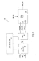
- Figure 1 is a block diagram of ADC circuit 100, according to one embodiment of the present invention.
- ADC circuit 100 includes a SD modulator 102, which receives input signal Vin, first reference signal Vref1 and second reference signal Vref2. As explained in further details below, SD modulator 102 can selectively use first reference signal Vref1 or second reference signal Vref2 to provide a PDM stream using SD modulation of input signal Vin.
- the PDM stream from SD modulator 102 may be selectively provided by multiplexer 103 as PDM_MSB stream or as PDM_LSB stream, representing the MSBs and the LSBs in the digital representation of input signal Vin, respectively.
- SD modulator 102 Under control of timing control unit 101, SD modulator 102 first samples input signal Vin and reference voltage Vref1 to provide through multiplexer 103 the PDM_MSB stream that represents the MSBs of the digital representation of input signal Vin ("SD phase"). After the oversample ratio for the MSBs (i.e., 2 N , where N is the number of bits in the MSBs) of clock cycles, under control of timing control unit 101, SD modulator 102 then stops sampling input signal Vin and uses reference voltage Vref2 to provide through multiplexer 103 the PDM_LSB stream that represents the LSBs of the digital representation of input signal Vin ("resolution-boosting phase").
- the sampled analog value is reduced to a "residual quantization error," which remains in capacitors of an integrator in SD modulator 102.
- the LSBs are provided over the oversampling ratio for the LSBs (i.e., 2 M , where M is the number of bits in the LSBs).
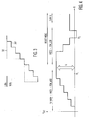
- Figure 3 shows the quantized steps for the MSBs (dotted graph 301) and the LSBs (solid graph 302), encoding 1 bit and 2 bits using reference signals Vref1 and Vref2, respectively, in accordance with one embodiment of the present invention.
- a further residual quantization error may still remain in the capacitors of an integrator in ADC circuit 100 (see, e.g., capacitors 204-1 and 204-2 of Figure 2 , described below). That residual quantization error may be positive or negative (indicated by signal Sign Q, and provides an additional bit of resolution after providing it an appropriate weight relative to the weight of the least significant bit.
- Digital filter 104 combines the Sign Q bit, the MSBs and the LSBs to provide the digital representation of input Vin as output value Data_out. As shown in Figure 1 , a Preload value is provided to digital filter 104, which sets a zero-crossing value in one embodiment, as discussed in further detail below with respect to Figure 2 .
- two conversions are performed on input signal Vin ("offset elimination mode"), one of which having the polarity of input signal Vin reversed.
- the difference of the two conversions represents twice the digital value of input signal Vin.
- Digital filter 104 combines the two sets of MSBs and LSBs to provide the digital representation of input Vin as output value Data_out.
- FIG. 2 shows schematically ADC circuit 200, which is one implementation of ADC 100, according to one embodiment of the present invention.
- multiplexers 201 and 202 sample the reference voltage (i.e., either Vref1 or Vref2) and input signal Vin (either polarity) into circuit 200.
- reference voltage Vref1 is selected; during the resolution-boosting phase, reference voltage Vref2 is selected.
- the first set of SD conversion selects input signal Vin, while the second set of SD conversion selects input signal -Vin.
- the sampled reference voltage and sampled input signal Vin are integrated in the integrator formed by differential amplifier 203 and capacitors 204-1 and 204-2.
- Switches 210-1 and 210-2 are closed to initiate the integration.
- the integrator may be reset by closing switches 205-1 and 205-2 momentarily to discharge capacitors 204-1 and 204-2.
- Comparator 206 detects when a predetermined threshold (e.g., the ground reference) is reached, provides an output pulse in its output PDM stream and determines the polarity of the reference sampling.
- a predetermined threshold e.g., the ground reference
- multiplexer 207 provides comparator 206's PDM stream as PDM1 stream; during the resolution-boosting phase, multiplexer 207 provides comparator 206's PDM stream as PDM2 stream.
- a further residual quantization error may still remain in capacitors 204-1 and 204-2 of the integrator in ADC circuit 200. That residual quantization error may be positive or negative, and is detected and indicated in signal Sign Q (or PDM3). This value may be used to provide an additional bit of resolution, after giving it an appropriate weight relative to the weight of the LSBs.
- FIG. 4 illustrates the voltage level in capacitor 204-1 or 204-2 during the SD phase and the resolution-boosting phase during the course of one conversion, according to one embodiment of the present invention.
- Counter 208 includes an MSB counter that increments whenever a pulse is detected in the PDM1 stream and an LSB counter that increments whenever a pulse is detected in the PDM2 stream.
- the combination of PDM streams and sign bit is achieved by a weighted sum of the PDM streams and a sign bit, using ripple up-counters. Due to circuit imperfections (e.g., asymmetric charge injection), the residual quantization error may be greater than one MSB. In that case, the quantization error is too large for the resolution-boosting phase.
- the second PDM stream (PDM2) is increased to have 2 M +X bits. The longer PDM stream causes a shift in the zero-crossing point in the ADC transfer curve. Preloading the ripple counter allows the zero-crossing point of the ADC transfer curve to be set to a desired value.
- the advantages of the present invention may be achieved using a system of only minimal extra circuitry.
- the present invention is able to perform faster, more accurate signal conversions, or both, as compared to a conventional 1 st order SD converter at the cost of a little extra circuitry.
Landscapes
- Engineering & Computer Science (AREA)
- Theoretical Computer Science (AREA)
- Compression, Expansion, Code Conversion, And Decoders (AREA)
- Analogue/Digital Conversion (AREA)
Abstract
Description
- The present application relates to and claims priority of U.S. provisional patent application ("Co-pending Provisional Patent Application"), serial
no. 61/824,819 - The present invention relates to an analog-to-digital converter (ADC) using a sigma delta modulation technique. In particular, the present invention relates to an ADC using a sigma delta (SD) modulation technique in which the number of clock cycles required for each conversion is not constrained by the oversampling ratio, unlike conventional 1st order SD converters.
- In a conventional 1st order SD ADC, the number of clock cycles necessary for each conversion is proportional to the oversampling ratio (OSR), which is given by OSR = 2N, where N is the number of bits in the digital output value. Thus, the conversion time doubles for each additional bit of resolution. To obtain a higher resolution without the exponential increase in conversion time, a higher-order SD converter may be used. However, such a SD ADC has a higher complexity and requires a greater converter area because of the higher-order decimation filters and the larger number of integrators required.
- Many approaches aimed at overcoming the OSR constraint have been tried. For example, the article "A 16-bit, 150 uW, 1kS/s ADC with hybrid incremental and cyclic conversion scheme" ("Rossi"), by L. Rossi et al., published in IEEE International Conference on Electronics, Circuits and Systems (ICECS 2009), Medina, Tunisia, December 13-16, 2009, discloses a circuit that uses an SD ADC to obtain the most significant bits (MSBs) and which applies a non-SD ADC -- in this case, a cyclic ADC -- on the residue to obtain the least significant bits (LSBs) in the output value.
-
U.S. Patent 5,936,562 , entitled "High-speed Sigma Delta ADCs" to Brooks et al., filed on June 6, 1997 and issued on August 10, 1999, also discloses applying a non-SD ADC on the residue to obtain the LSBs in the output value. -
U.S. Patent 7,511,648 , entitled "Integrating/SAR and Method with Low Integrator Swing and Low Complexity" ("Trifonov"), to D. Trifonov et al., discloses a hybrid approach that uses both SD modulation and non-SD techniques. In this case, the non-SD technique is a successive approximation register (SAR) technique. However, Trifinov's approach requires a control unit to implement the SAR algorithm, a multiply-by-2 circuit, and a complex circuit for combining the results of the SD and the non-SD conversions. - The present invention provides a method and an ADC circuit that use more than one SD modulation on an analog value, and then applies digital post-processing of the pulse density modulation (PDM) streams from the SD modulations to obtain a higher resolution in the digital output value for a given oversampling ratio. According to one embodiment of the present invention, the SD ADC does not face the constraint of conversion time doubling for each additional bit of resolution. In an SD ADC of the present invention, the conversion includes a SD phase and a resolution-boosting phase. During the SD phase, the MSBs of the digital output value are generated from the sampled analog value using a first SD conversion. At the end of the SD phase, the sampled analog value is reduced to a "residual quantization error," which remains in a capacitor of an integrator of the SD ADC. In the resolution-boosting phase, the LSBs of the digital output value are generated from the residual quantization error using a second SD conversion that provides at least the LSBs. The second SD conversion may be carried out using the same SD ADC as the SD ADC used in the SD phase, except a different set of reference voltages or capacitor values, or both, are used. The reference voltage and capacitor values for each SD conversion are selected based on the analog values and weights represented by the corresponding bits.
- According to one embodiment of the present invention, the SD modulator generates, in time-interleaved operations, a first pulse density modulation (PDM) stream and one or more PDM streams, representing the MSBs and LSBs of the digital output value, respectively. The digital output value is obtained by combining in a digital filter the bits represented by the two PDM streams. In one implementation, the combination is achieved as a weighted sum of the MSBs and the LSBs using only ripple up-counters with separate weighting for the PDM streams. Preloading the ripple up-counters eliminates the need for costly up-down counters and allows a zero-crossing point to be set as required in the ADC transfer curve. By using the same SD modulator to generate a number of PDM streams and combining these PDM streams in ripple up-counters, the advantages of the present invention are achieved in a system requiring only a minimal amount of extra circuitry, as compared to a conventional 1st order SD converter.
- According to one embodiment of the present invention, an algorithm which cancels offsets in the SD conversions may be used.
- The present invention is better understood upon consideration of the detailed description below in conjunction with the accompanying drawings.
-
-
Figure 1 is a block diagram ofADC circuit 100, according to one embodiment of the present invention. -
Figure 2 shows schematicallyADC circuit 200, which is one implementation ofADC 100, according to one embodiment of the present invention. -
Figure 3 shows the quantized steps for the MSBs (dotted graph 301) and the LSBs (solid graph 302), encoding 1 bit and 2 bits using reference signals Vref1 and Vref2, respectively, in accordance with one embodiment of the present invention. -
Figure 4 illustrates the voltage level in capacitor 204-1 or 204-2 during the SD phase and the resolution-boosting phase during the course of one conversion, according to one embodiment of the present invention. - The present invention provides a method and an ADC circuit that use more than one SD modulation on an analog value, and then applies digital post-processing of the pulse density modulation (PDM) streams from the SD modulations to obtain a higher resolution in the digital output value for a given oversampling ratio.
Figure 1 is a block diagram ofADC circuit 100, according to one embodiment of the present invention. - As shown in
Figure 1 ,ADC circuit 100 includes aSD modulator 102, which receives input signal Vin, first reference signal Vref1 and second reference signal Vref2. As explained in further details below,SD modulator 102 can selectively use first reference signal Vref1 or second reference signal Vref2 to provide a PDM stream using SD modulation of input signal Vin. The PDM stream fromSD modulator 102 may be selectively provided bymultiplexer 103 as PDM_MSB stream or as PDM_LSB stream, representing the MSBs and the LSBs in the digital representation of input signal Vin, respectively. Under control oftiming control unit 101,SD modulator 102 first samples input signal Vin and reference voltage Vref1 to provide throughmultiplexer 103 the PDM_MSB stream that represents the MSBs of the digital representation of input signal Vin ("SD phase"). After the oversample ratio for the MSBs (i.e., 2N, where N is the number of bits in the MSBs) of clock cycles, under control oftiming control unit 101,SD modulator 102 then stops sampling input signal Vin and uses reference voltage Vref2 to provide throughmultiplexer 103 the PDM_LSB stream that represents the LSBs of the digital representation of input signal Vin ("resolution-boosting phase"). At the end of the SD phase, the sampled analog value is reduced to a "residual quantization error," which remains in capacitors of an integrator inSD modulator 102. During the resolution boosting phase, the LSBs are provided over the oversampling ratio for the LSBs (i.e., 2M, where M is the number of bits in the LSBs).Figure 3 shows the quantized steps for the MSBs (dotted graph 301) and the LSBs (solid graph 302), encoding 1 bit and 2 bits using reference signals Vref1 and Vref2, respectively, in accordance with one embodiment of the present invention. At the end of the 2M clock cycles in the resolution-boosting phase, a further residual quantization error may still remain in the capacitors of an integrator in ADC circuit 100 (see, e.g., capacitors 204-1 and 204-2 ofFigure 2 , described below). That residual quantization error may be positive or negative (indicated by signal Sign Q, and provides an additional bit of resolution after providing it an appropriate weight relative to the weight of the least significant bit.Digital filter 104 combines the Sign Q bit, the MSBs and the LSBs to provide the digital representation of input Vin as output value Data_out. As shown inFigure 1 , a Preload value is provided todigital filter 104, which sets a zero-crossing value in one embodiment, as discussed in further detail below with respect toFigure 2 . - In one embodiment, two conversions are performed on input signal Vin ("offset elimination mode"), one of which having the polarity of input signal Vin reversed. The difference of the two conversions represents twice the digital value of input signal Vin. Using this technique, any offset voltage in
ADC circuit 100 may be eliminated.Digital filter 104 combines the two sets of MSBs and LSBs to provide the digital representation of input Vin as output value Data_out. -
Figure 2 shows schematicallyADC circuit 200, which is one implementation ofADC 100, according to one embodiment of the present invention. As shown inFigure 2 ,multiplexers circuit 200. During the SD phase, reference voltage Vref1 is selected; during the resolution-boosting phase, reference voltage Vref2 is selected. In offset elimination mode, the first set of SD conversion selects input signal Vin, while the second set of SD conversion selects input signal -Vin. The sampled reference voltage and sampled input signal Vin are integrated in the integrator formed bydifferential amplifier 203 and capacitors 204-1 and 204-2. Switches 210-1 and 210-2 are closed to initiate the integration. The integrator may be reset by closing switches 205-1 and 205-2 momentarily to discharge capacitors 204-1 and 204-2. Comparator 206 detects when a predetermined threshold (e.g., the ground reference) is reached, provides an output pulse in its output PDM stream and determines the polarity of the reference sampling. At the end of the SD phase, the sampled analog value is reduced to a "residual quantization error," which remains in capacitors 204-1 and 204-2 of the integrator inADC circuit 200. During the SD phase,multiplexer 207 provides comparator 206's PDM stream as PDM1 stream; during the resolution-boosting phase,multiplexer 207 provides comparator 206's PDM stream as PDM2 stream. After 2M clock cycles in the resolution-boosting phase, a further residual quantization error may still remain in capacitors 204-1 and 204-2 of the integrator inADC circuit 200. That residual quantization error may be positive or negative, and is detected and indicated in signal Sign Q (or PDM3). This value may be used to provide an additional bit of resolution, after giving it an appropriate weight relative to the weight of the LSBs.Figure 4 illustrates the voltage level in capacitor 204-1 or 204-2 during the SD phase and the resolution-boosting phase during the course of one conversion, according to one embodiment of the present invention.Counter 208 includes an MSB counter that increments whenever a pulse is detected in the PDM1 stream and an LSB counter that increments whenever a pulse is detected in the PDM2 stream. - In one implementation, the combination of PDM streams and sign bit is achieved by a weighted sum of the PDM streams and a sign bit, using ripple up-counters. Due to circuit imperfections (e.g., asymmetric charge injection), the residual quantization error may be greater than one MSB. In that case, the quantization error is too large for the resolution-boosting phase. To extend the signal range of the resolution-boosting phase, the second PDM stream (PDM2) is increased to have 2M +X bits. The longer PDM stream causes a shift in the zero-crossing point in the ADC transfer curve. Preloading the ripple counter allows the zero-crossing point of the ADC transfer curve to be set to a desired value. Using the same SD modulator to generate the N PDM streams and a sign bit, and combining these PDM streams in ripple up-counters, the advantages of the present invention may be achieved using a system of only minimal extra circuitry. The present invention is able to perform faster, more accurate signal conversions, or both, as compared to a conventional 1st order SD converter at the cost of a little extra circuitry.
- The above detailed description is provided to illustrate the specific embodiments of the present invention and is not intended to be limiting. Numerous variations and modifications within the scope of the present invention are possible. The present invention is set forth in the accompanying claims.
Claims (13)
- An analog-to-digital converter (ADC) receiving an analog signal as input and providing an output digital value representative of the analog signal, comprising:a first multiplexer receiving two or more reference signals to provide a selected reference signal;a sigma delta modulator receiving the selected reference signal and the analog signal to provide a set of pulses representative of the analog signal received;a control circuit causing the first multiplexer to select (i) in a first phase of a conversion, a first one of the reference signals as the selected reference signal and (ii) in subsequent phases of the conversion, the other reference signals, one at a time, as the selected reference signal, such that the sigma delta modulator provides, respectively, a first set of pulses in the first phase and an additional set of pulses in each of the subsequent phases of the conversion; anda digital filter receiving in each conversion the first set and the subsequent sets of pulses to provide the digital output value.
- The ADC of Claim 1, wherein the first set of pulses represents the most significant bits of the digital output value, and wherein the additional sets of pulses represent the least significant bits of the output digital value.
- The ADC of Claim 1 or 2, a second multiplexer selectively providing the analog signal in a first polarity and in a second polarity that is opposite the first polarity.
- The ADC of Claim 3, wherein the control circuit performs a first conversion and a second conversion using, respectively, the analog signal in the first polarity and the analog signal in the second polarity, and wherein the digital filter provides a final output digital value based on the respective digital output values obtained in the first and second conversions.
- The ADC of any of the preceding Claims, wherein the digital filter comprises one or more up-counters that are reset and preloaded with one or more predetermined values before each conversion, so as to adjust a zero-crossing point in an ADC transfer curve.
- The ADC of any of the preceding Claims, wherein the sigma delta modulator in each subsequent phase converts a residual quantization error.
- The ADC of Claim 6, wherein at the end of each subsequent phase, the polarity of the residual quantization error then present is used to further refine the output digital value.
- A method for analog-to-digital conversion of an analog signal as input to provide an output digital value representative of the analog signal, comprising:in a first multiplexer, selecting as a selected reference signal (i) a first reference signal in a first phase of conversion, and (ii) one or more reference signals, one at a time, in subsequent phases of the conversion;providing the analog signal and the selected reference signal to a sigma delta modulator to create, respectively, a first set of pulses and an additional set of pulses in the first phase and each of the subsequent phases, respectively; andcombining in a digital filter the first set and the subsequent sets of pulses to provide the output digital value.
- The method of Claim 8, wherein the first set of pulses represents the most significant bits of the output digital value, and wherein the additional sets of pulses represent the least significant bits of the output digital value.
- The method of Claim 8 or 9, wherein the method performs a first analog-to-digital conversion and a second analog-to-digital conversion, in which the first analog-to-digital conversion provides the analog signal in the first polarity and the second analog-to-digital conversion is performed with the analog signal in the second polarity opposite the first polarity, and wherein the digital filter provides the output digital value based on the digital output values corresponding to the first and second analog-to-digital conversions.
- The method of any of Claims 8-10, wherein the digital filter comprises one or more up-counters that are reset and preloaded with one or more predetermined values before each conversion, so as to adjust a zero-crossing point in an ADC transfer curve.
- The method of any of Claims 8-11, wherein the analog signal received into the sigma delta modulator in each of the subsequent phases of the conversion represents a residual quantization error.
- The method of Claim 12, further comprising, at the end of each of the subsequent phases, refining the output digital value using the polarity of the residual quantization error then present.
Applications Claiming Priority (2)
| Application Number | Priority Date | Filing Date | Title |
|---|---|---|---|
| US201361824819P | 2013-05-17 | 2013-05-17 | |
| US14/052,479 US9077374B2 (en) | 2013-05-17 | 2013-10-11 | Resolution-boosted sigma delta analog-to-digital converter |
Publications (3)
| Publication Number | Publication Date |
|---|---|
| EP2811654A2 true EP2811654A2 (en) | 2014-12-10 |
| EP2811654A3 EP2811654A3 (en) | 2014-12-24 |
| EP2811654B1 EP2811654B1 (en) | 2019-07-03 |
Family
ID=50729338
Family Applications (1)
| Application Number | Title | Priority Date | Filing Date |
|---|---|---|---|
| EP14001697.3A Active EP2811654B1 (en) | 2013-05-17 | 2014-05-14 | Resolution-boosted sigma delta analog-to-digital converter |
Country Status (2)
| Country | Link |
|---|---|
| US (1) | US9077374B2 (en) |
| EP (1) | EP2811654B1 (en) |
Families Citing this family (6)
| Publication number | Priority date | Publication date | Assignee | Title |
|---|---|---|---|---|
| KR20170010515A (en) | 2015-07-20 | 2017-02-01 | 삼성전자주식회사 | Semiconductor device comprising Successive Approximation Register Analog to Digital Converter and Integrator |
| US9768792B1 (en) * | 2016-12-30 | 2017-09-19 | Itron, Inc. | Asynchronous sigma-delta analog-to-digital converter |
| US10459856B2 (en) | 2016-12-30 | 2019-10-29 | Itron, Inc. | Variable acquisition buffer length |
| US10509624B2 (en) * | 2017-01-30 | 2019-12-17 | Cirrus Logic, Inc. | Single-bit volume control |
| EP4207604A1 (en) * | 2022-01-03 | 2023-07-05 | STMicroelectronics S.r.l. | Analog to digital converter apparatus with time continuous input and corresponding method |
| CN116054836A (en) * | 2023-01-13 | 2023-05-02 | 思瑞浦微电子科技(苏州)股份有限公司 | Three-step zoom ADC and analog-to-digital conversion method |
Citations (2)
| Publication number | Priority date | Publication date | Assignee | Title |
|---|---|---|---|---|
| US5936562A (en) | 1997-06-06 | 1999-08-10 | Analog Devices, Inc. | High-speed sigma-delta ADCs |
| US7511648B2 (en) | 2007-04-23 | 2009-03-31 | Texas Instruments Incorporated | Integrating/SAR ADC and method with low integrator swing and low complexity |
Family Cites Families (2)
| Publication number | Priority date | Publication date | Assignee | Title |
|---|---|---|---|---|
| US5440305A (en) * | 1992-08-31 | 1995-08-08 | Crystal Semiconductor Corporation | Method and apparatus for calibration of a monolithic voltage reference |
| US6614375B2 (en) * | 2001-09-19 | 2003-09-02 | Texas Instruments Incorporated | Sigma-delta analog-to-digital converter having improved reference multiplexer |
-
2013
- 2013-10-11 US US14/052,479 patent/US9077374B2/en active Active
-
2014
- 2014-05-14 EP EP14001697.3A patent/EP2811654B1/en active Active
Patent Citations (2)
| Publication number | Priority date | Publication date | Assignee | Title |
|---|---|---|---|---|
| US5936562A (en) | 1997-06-06 | 1999-08-10 | Analog Devices, Inc. | High-speed sigma-delta ADCs |
| US7511648B2 (en) | 2007-04-23 | 2009-03-31 | Texas Instruments Incorporated | Integrating/SAR ADC and method with low integrator swing and low complexity |
Non-Patent Citations (1)
| Title |
|---|
| L. ROSSI ET AL., IEEE INTERNATIONAL CONFERENCE ON ELECTRONICS, CIRCUITS AND SYSTEMS (ICECS 2009, 13 December 2009 (2009-12-13) |
Also Published As
| Publication number | Publication date |
|---|---|
| EP2811654B1 (en) | 2019-07-03 |
| US20140340248A1 (en) | 2014-11-20 |
| US9077374B2 (en) | 2015-07-07 |
| EP2811654A3 (en) | 2014-12-24 |
Similar Documents
| Publication | Publication Date | Title |
|---|---|---|
| EP2811654B1 (en) | Resolution-boosted sigma delta analog-to-digital converter | |
| US7515084B1 (en) | Analog to digital converter using asynchronous pulse technology | |
| US6958722B1 (en) | SAR ADC providing digital codes with high accuracy and high throughput performance | |
| US8508399B2 (en) | Successive approximation analog to digital converter and method of analog to digital conversion | |
| US10886937B1 (en) | Method to embed ELD DAC in SAR quantizer | |
| JP6353267B2 (en) | AD converter and AD conversion method | |
| US20180183450A1 (en) | Interleaving successive approximation analog-to-digital converter with noise shaping | |
| US10312926B2 (en) | Noise-shaping analog-to-digital converter | |
| US10027343B2 (en) | Circuit and method for generating reference signals for hybrid analog-to-digital convertors | |
| EP2538562B1 (en) | Simultaneously-sampling single-ended and differential two-input analog-to-digital converter | |
| KR20150027582A (en) | Successive approximation analog to digital converter and method of analog to digital conversion | |
| CN105720979B (en) | Calibration techniques for SAR ADCs with on-chip energy storage capacitors | |
| KR101204521B1 (en) | Analog signal sampling system and method having reduced average input current | |
| US6795007B2 (en) | Circuits and methods for a variable over sample ratio delta-sigma analog-to-digital converter | |
| US10056916B2 (en) | Analog/digital conversion with analog filtering | |
| CN112511167A (en) | Low noise analog-to-digital converter | |
| US7102559B2 (en) | Analog-to-digital converter having interleaved coarse sections coupled to a single fine section | |
| Kościelnik et al. | Time-to-digital converters based on event-driven successive charge redistribution: A theoretical approach | |
| CN112104370B (en) | High-precision analog-to-digital converter conversion speed improving circuit | |
| CN111934685B (en) | Improved interleaving method for analog-to-digital converters | |
| JP4684028B2 (en) | Pipeline A / D converter | |
| US9007253B2 (en) | Successive-approximation-register analog-to-digital converter and method thereof | |
| US12470230B2 (en) | Systems and methods for precharging driver circuitry for an analog-to-digital converter | |
| Hernandez et al. | Continuous time sigma-delta modulator based on binary weighted charge balance | |
| JP2018125651A (en) | Incremental delta-sigma ad converter and ad conversion method |
Legal Events
| Date | Code | Title | Description |
|---|---|---|---|
| PUAL | Search report despatched |
Free format text: ORIGINAL CODE: 0009013 |
|
| PUAI | Public reference made under article 153(3) epc to a published international application that has entered the european phase |
Free format text: ORIGINAL CODE: 0009012 |
|
| 17P | Request for examination filed |
Effective date: 20140514 |
|
| AK | Designated contracting states |
Kind code of ref document: A2 Designated state(s): AL AT BE BG CH CY CZ DE DK EE ES FI FR GB GR HR HU IE IS IT LI LT LU LV MC MK MT NL NO PL PT RO RS SE SI SK SM TR |
|
| AX | Request for extension of the european patent |
Extension state: BA ME |
|
| AK | Designated contracting states |
Kind code of ref document: A3 Designated state(s): AL AT BE BG CH CY CZ DE DK EE ES FI FR GB GR HR HU IE IS IT LI LT LU LV MC MK MT NL NO PL PT RO RS SE SI SK SM TR |
|
| AX | Request for extension of the european patent |
Extension state: BA ME |
|
| RIC1 | Information provided on ipc code assigned before grant |
Ipc: H03M 3/00 20060101AFI20141117BHEP |
|
| R17P | Request for examination filed (corrected) |
Effective date: 20150623 |
|
| RBV | Designated contracting states (corrected) |
Designated state(s): AL AT BE BG CH CY CZ DE DK EE ES FI FR GB GR HR HU IE IS IT LI LT LU LV MC MK MT NL NO PL PT RO RS SE SI SK SM TR |
|
| STAA | Information on the status of an ep patent application or granted ep patent |
Free format text: STATUS: EXAMINATION IS IN PROGRESS |
|
| 17Q | First examination report despatched |
Effective date: 20180307 |
|
| GRAP | Despatch of communication of intention to grant a patent |
Free format text: ORIGINAL CODE: EPIDOSNIGR1 |
|
| STAA | Information on the status of an ep patent application or granted ep patent |
Free format text: STATUS: GRANT OF PATENT IS INTENDED |
|
| INTG | Intention to grant announced |
Effective date: 20181219 |
|
| GRAS | Grant fee paid |
Free format text: ORIGINAL CODE: EPIDOSNIGR3 |
|
| GRAA | (expected) grant |
Free format text: ORIGINAL CODE: 0009210 |
|
| STAA | Information on the status of an ep patent application or granted ep patent |
Free format text: STATUS: THE PATENT HAS BEEN GRANTED |
|
| AK | Designated contracting states |
Kind code of ref document: B1 Designated state(s): AL AT BE BG CH CY CZ DE DK EE ES FI FR GB GR HR HU IE IS IT LI LT LU LV MC MK MT NL NO PL PT RO RS SE SI SK SM TR |
|
| REG | Reference to a national code |
Ref country code: GB Ref legal event code: FG4D |
|
| REG | Reference to a national code |
Ref country code: CH Ref legal event code: EP Ref country code: AT Ref legal event code: REF Ref document number: 1152223 Country of ref document: AT Kind code of ref document: T Effective date: 20190715 |
|
| REG | Reference to a national code |
Ref country code: IE Ref legal event code: FG4D |
|
| REG | Reference to a national code |
Ref country code: DE Ref legal event code: R096 Ref document number: 602014049333 Country of ref document: DE |
|
| REG | Reference to a national code |
Ref country code: NL Ref legal event code: MP Effective date: 20190703 |
|
| REG | Reference to a national code |
Ref country code: LT Ref legal event code: MG4D |
|
| REG | Reference to a national code |
Ref country code: AT Ref legal event code: MK05 Ref document number: 1152223 Country of ref document: AT Kind code of ref document: T Effective date: 20190703 |
|
| PG25 | Lapsed in a contracting state [announced via postgrant information from national office to epo] |
Ref country code: FI Free format text: LAPSE BECAUSE OF FAILURE TO SUBMIT A TRANSLATION OF THE DESCRIPTION OR TO PAY THE FEE WITHIN THE PRESCRIBED TIME-LIMIT Effective date: 20190703 Ref country code: LT Free format text: LAPSE BECAUSE OF FAILURE TO SUBMIT A TRANSLATION OF THE DESCRIPTION OR TO PAY THE FEE WITHIN THE PRESCRIBED TIME-LIMIT Effective date: 20190703 Ref country code: PT Free format text: LAPSE BECAUSE OF FAILURE TO SUBMIT A TRANSLATION OF THE DESCRIPTION OR TO PAY THE FEE WITHIN THE PRESCRIBED TIME-LIMIT Effective date: 20191104 Ref country code: HR Free format text: LAPSE BECAUSE OF FAILURE TO SUBMIT A TRANSLATION OF THE DESCRIPTION OR TO PAY THE FEE WITHIN THE PRESCRIBED TIME-LIMIT Effective date: 20190703 Ref country code: CZ Free format text: LAPSE BECAUSE OF FAILURE TO SUBMIT A TRANSLATION OF THE DESCRIPTION OR TO PAY THE FEE WITHIN THE PRESCRIBED TIME-LIMIT Effective date: 20190703 Ref country code: NO Free format text: LAPSE BECAUSE OF FAILURE TO SUBMIT A TRANSLATION OF THE DESCRIPTION OR TO PAY THE FEE WITHIN THE PRESCRIBED TIME-LIMIT Effective date: 20191003 Ref country code: BG Free format text: LAPSE BECAUSE OF FAILURE TO SUBMIT A TRANSLATION OF THE DESCRIPTION OR TO PAY THE FEE WITHIN THE PRESCRIBED TIME-LIMIT Effective date: 20191003 Ref country code: NL Free format text: LAPSE BECAUSE OF FAILURE TO SUBMIT A TRANSLATION OF THE DESCRIPTION OR TO PAY THE FEE WITHIN THE PRESCRIBED TIME-LIMIT Effective date: 20190703 Ref country code: AT Free format text: LAPSE BECAUSE OF FAILURE TO SUBMIT A TRANSLATION OF THE DESCRIPTION OR TO PAY THE FEE WITHIN THE PRESCRIBED TIME-LIMIT Effective date: 20190703 Ref country code: SE Free format text: LAPSE BECAUSE OF FAILURE TO SUBMIT A TRANSLATION OF THE DESCRIPTION OR TO PAY THE FEE WITHIN THE PRESCRIBED TIME-LIMIT Effective date: 20190703 |
|
| PG25 | Lapsed in a contracting state [announced via postgrant information from national office to epo] |
Ref country code: IS Free format text: LAPSE BECAUSE OF FAILURE TO SUBMIT A TRANSLATION OF THE DESCRIPTION OR TO PAY THE FEE WITHIN THE PRESCRIBED TIME-LIMIT Effective date: 20191103 Ref country code: GR Free format text: LAPSE BECAUSE OF FAILURE TO SUBMIT A TRANSLATION OF THE DESCRIPTION OR TO PAY THE FEE WITHIN THE PRESCRIBED TIME-LIMIT Effective date: 20191004 Ref country code: ES Free format text: LAPSE BECAUSE OF FAILURE TO SUBMIT A TRANSLATION OF THE DESCRIPTION OR TO PAY THE FEE WITHIN THE PRESCRIBED TIME-LIMIT Effective date: 20190703 Ref country code: RS Free format text: LAPSE BECAUSE OF FAILURE TO SUBMIT A TRANSLATION OF THE DESCRIPTION OR TO PAY THE FEE WITHIN THE PRESCRIBED TIME-LIMIT Effective date: 20190703 Ref country code: LV Free format text: LAPSE BECAUSE OF FAILURE TO SUBMIT A TRANSLATION OF THE DESCRIPTION OR TO PAY THE FEE WITHIN THE PRESCRIBED TIME-LIMIT Effective date: 20190703 Ref country code: AL Free format text: LAPSE BECAUSE OF FAILURE TO SUBMIT A TRANSLATION OF THE DESCRIPTION OR TO PAY THE FEE WITHIN THE PRESCRIBED TIME-LIMIT Effective date: 20190703 |
|
| PG25 | Lapsed in a contracting state [announced via postgrant information from national office to epo] |
Ref country code: TR Free format text: LAPSE BECAUSE OF FAILURE TO SUBMIT A TRANSLATION OF THE DESCRIPTION OR TO PAY THE FEE WITHIN THE PRESCRIBED TIME-LIMIT Effective date: 20190703 |
|
| PG25 | Lapsed in a contracting state [announced via postgrant information from national office to epo] |
Ref country code: IT Free format text: LAPSE BECAUSE OF FAILURE TO SUBMIT A TRANSLATION OF THE DESCRIPTION OR TO PAY THE FEE WITHIN THE PRESCRIBED TIME-LIMIT Effective date: 20190703 Ref country code: DK Free format text: LAPSE BECAUSE OF FAILURE TO SUBMIT A TRANSLATION OF THE DESCRIPTION OR TO PAY THE FEE WITHIN THE PRESCRIBED TIME-LIMIT Effective date: 20190703 Ref country code: RO Free format text: LAPSE BECAUSE OF FAILURE TO SUBMIT A TRANSLATION OF THE DESCRIPTION OR TO PAY THE FEE WITHIN THE PRESCRIBED TIME-LIMIT Effective date: 20190703 Ref country code: EE Free format text: LAPSE BECAUSE OF FAILURE TO SUBMIT A TRANSLATION OF THE DESCRIPTION OR TO PAY THE FEE WITHIN THE PRESCRIBED TIME-LIMIT Effective date: 20190703 Ref country code: PL Free format text: LAPSE BECAUSE OF FAILURE TO SUBMIT A TRANSLATION OF THE DESCRIPTION OR TO PAY THE FEE WITHIN THE PRESCRIBED TIME-LIMIT Effective date: 20190703 |
|
| PG25 | Lapsed in a contracting state [announced via postgrant information from national office to epo] |
Ref country code: SK Free format text: LAPSE BECAUSE OF FAILURE TO SUBMIT A TRANSLATION OF THE DESCRIPTION OR TO PAY THE FEE WITHIN THE PRESCRIBED TIME-LIMIT Effective date: 20190703 Ref country code: SM Free format text: LAPSE BECAUSE OF FAILURE TO SUBMIT A TRANSLATION OF THE DESCRIPTION OR TO PAY THE FEE WITHIN THE PRESCRIBED TIME-LIMIT Effective date: 20190703 Ref country code: IS Free format text: LAPSE BECAUSE OF FAILURE TO SUBMIT A TRANSLATION OF THE DESCRIPTION OR TO PAY THE FEE WITHIN THE PRESCRIBED TIME-LIMIT Effective date: 20200224 |
|
| REG | Reference to a national code |
Ref country code: DE Ref legal event code: R097 Ref document number: 602014049333 Country of ref document: DE |
|
| PLBE | No opposition filed within time limit |
Free format text: ORIGINAL CODE: 0009261 |
|
| STAA | Information on the status of an ep patent application or granted ep patent |
Free format text: STATUS: NO OPPOSITION FILED WITHIN TIME LIMIT |
|
| PG2D | Information on lapse in contracting state deleted |
Ref country code: IS |
|
| 26N | No opposition filed |
Effective date: 20200603 |
|
| PG25 | Lapsed in a contracting state [announced via postgrant information from national office to epo] |
Ref country code: SI Free format text: LAPSE BECAUSE OF FAILURE TO SUBMIT A TRANSLATION OF THE DESCRIPTION OR TO PAY THE FEE WITHIN THE PRESCRIBED TIME-LIMIT Effective date: 20190703 |
|
| PG25 | Lapsed in a contracting state [announced via postgrant information from national office to epo] |
Ref country code: MC Free format text: LAPSE BECAUSE OF FAILURE TO SUBMIT A TRANSLATION OF THE DESCRIPTION OR TO PAY THE FEE WITHIN THE PRESCRIBED TIME-LIMIT Effective date: 20190703 Ref country code: CH Free format text: LAPSE BECAUSE OF NON-PAYMENT OF DUE FEES Effective date: 20200531 Ref country code: LI Free format text: LAPSE BECAUSE OF NON-PAYMENT OF DUE FEES Effective date: 20200531 |
|
| REG | Reference to a national code |
Ref country code: BE Ref legal event code: MM Effective date: 20200531 |
|
| GBPC | Gb: european patent ceased through non-payment of renewal fee |
Effective date: 20200514 |
|
| PG25 | Lapsed in a contracting state [announced via postgrant information from national office to epo] |
Ref country code: LU Free format text: LAPSE BECAUSE OF NON-PAYMENT OF DUE FEES Effective date: 20200514 |
|
| PG25 | Lapsed in a contracting state [announced via postgrant information from national office to epo] |
Ref country code: IE Free format text: LAPSE BECAUSE OF NON-PAYMENT OF DUE FEES Effective date: 20200514 Ref country code: GB Free format text: LAPSE BECAUSE OF NON-PAYMENT OF DUE FEES Effective date: 20200514 Ref country code: FR Free format text: LAPSE BECAUSE OF NON-PAYMENT OF DUE FEES Effective date: 20200531 |
|
| REG | Reference to a national code |
Ref country code: DE Ref legal event code: R082 Ref document number: 602014049333 Country of ref document: DE Representative=s name: MUELLER-BORE & PARTNER PATENTANWAELTE PARTG MB, DE Ref country code: DE Ref legal event code: R081 Ref document number: 602014049333 Country of ref document: DE Owner name: ANALOG DEVICES INTERNATIONAL UNLIMITED COMPANY, IE Free format text: FORMER OWNER: LINEAR TECHNOLOGY CORPORATION, MILPITAS, CALIF., US Ref country code: DE Ref legal event code: R082 Ref document number: 602014049333 Country of ref document: DE Representative=s name: WITHERS & ROGERS LLP, DE |
|
| PG25 | Lapsed in a contracting state [announced via postgrant information from national office to epo] |
Ref country code: BE Free format text: LAPSE BECAUSE OF NON-PAYMENT OF DUE FEES Effective date: 20200531 |
|
| REG | Reference to a national code |
Ref country code: DE Ref legal event code: R082 Ref document number: 602014049333 Country of ref document: DE Representative=s name: WITHERS & ROGERS LLP, DE |
|
| PG25 | Lapsed in a contracting state [announced via postgrant information from national office to epo] |
Ref country code: MT Free format text: LAPSE BECAUSE OF FAILURE TO SUBMIT A TRANSLATION OF THE DESCRIPTION OR TO PAY THE FEE WITHIN THE PRESCRIBED TIME-LIMIT Effective date: 20190703 Ref country code: CY Free format text: LAPSE BECAUSE OF FAILURE TO SUBMIT A TRANSLATION OF THE DESCRIPTION OR TO PAY THE FEE WITHIN THE PRESCRIBED TIME-LIMIT Effective date: 20190703 |
|
| PG25 | Lapsed in a contracting state [announced via postgrant information from national office to epo] |
Ref country code: MK Free format text: LAPSE BECAUSE OF FAILURE TO SUBMIT A TRANSLATION OF THE DESCRIPTION OR TO PAY THE FEE WITHIN THE PRESCRIBED TIME-LIMIT Effective date: 20190703 |
|
| PGFP | Annual fee paid to national office [announced via postgrant information from national office to epo] |
Ref country code: DE Payment date: 20250423 Year of fee payment: 12 |