EP2811579A1 - Connector - Google Patents
Connector Download PDFInfo
- Publication number
- EP2811579A1 EP2811579A1 EP14170272.0A EP14170272A EP2811579A1 EP 2811579 A1 EP2811579 A1 EP 2811579A1 EP 14170272 A EP14170272 A EP 14170272A EP 2811579 A1 EP2811579 A1 EP 2811579A1
- Authority
- EP
- European Patent Office
- Prior art keywords
- contacts
- contact
- contact holder
- main body
- connector
- Prior art date
- Legal status (The legal status is an assumption and is not a legal conclusion. Google has not performed a legal analysis and makes no representation as to the accuracy of the status listed.)
- Granted
Links
Images


Classifications
-
- H—ELECTRICITY
- H01—ELECTRIC ELEMENTS
- H01R—ELECTRICALLY-CONDUCTIVE CONNECTIONS; STRUCTURAL ASSOCIATIONS OF A PLURALITY OF MUTUALLY-INSULATED ELECTRICAL CONNECTING ELEMENTS; COUPLING DEVICES; CURRENT COLLECTORS
- H01R12/00—Structural associations of a plurality of mutually-insulated electrical connecting elements, specially adapted for printed circuits, e.g. printed circuit boards [PCB], flat or ribbon cables, or like generally planar structures, e.g. terminal strips, terminal blocks; Coupling devices specially adapted for printed circuits, flat or ribbon cables, or like generally planar structures; Terminals specially adapted for contact with, or insertion into, printed circuits, flat or ribbon cables, or like generally planar structures
- H01R12/70—Coupling devices
-
- H—ELECTRICITY
- H01—ELECTRIC ELEMENTS
- H01R—ELECTRICALLY-CONDUCTIVE CONNECTIONS; STRUCTURAL ASSOCIATIONS OF A PLURALITY OF MUTUALLY-INSULATED ELECTRICAL CONNECTING ELEMENTS; COUPLING DEVICES; CURRENT COLLECTORS
- H01R13/00—Details of coupling devices of the kinds covered by groups H01R12/70 or H01R24/00 - H01R33/00
- H01R13/40—Securing contact members in or to a base or case; Insulating of contact members
- H01R13/405—Securing in non-demountable manner, e.g. moulding, riveting
-
- H—ELECTRICITY
- H01—ELECTRIC ELEMENTS
- H01R—ELECTRICALLY-CONDUCTIVE CONNECTIONS; STRUCTURAL ASSOCIATIONS OF A PLURALITY OF MUTUALLY-INSULATED ELECTRICAL CONNECTING ELEMENTS; COUPLING DEVICES; CURRENT COLLECTORS
- H01R13/00—Details of coupling devices of the kinds covered by groups H01R12/70 or H01R24/00 - H01R33/00
- H01R13/46—Bases; Cases
- H01R13/514—Bases; Cases composed as a modular blocks or assembly, i.e. composed of co-operating parts provided with contact members or holding contact members between them
-
- H—ELECTRICITY
- H01—ELECTRIC ELEMENTS
- H01R—ELECTRICALLY-CONDUCTIVE CONNECTIONS; STRUCTURAL ASSOCIATIONS OF A PLURALITY OF MUTUALLY-INSULATED ELECTRICAL CONNECTING ELEMENTS; COUPLING DEVICES; CURRENT COLLECTORS
- H01R13/00—Details of coupling devices of the kinds covered by groups H01R12/70 or H01R24/00 - H01R33/00
- H01R13/46—Bases; Cases
- H01R13/516—Means for holding or embracing insulating body, e.g. casing, hoods
-
- H—ELECTRICITY
- H01—ELECTRIC ELEMENTS
- H01R—ELECTRICALLY-CONDUCTIVE CONNECTIONS; STRUCTURAL ASSOCIATIONS OF A PLURALITY OF MUTUALLY-INSULATED ELECTRICAL CONNECTING ELEMENTS; COUPLING DEVICES; CURRENT COLLECTORS
- H01R24/00—Two-part coupling devices, or either of their cooperating parts, characterised by their overall structure
- H01R24/60—Contacts spaced along planar side wall transverse to longitudinal axis of engagement
Definitions
- This disclosure relates to a connector having a plurality of contacts.
- a connector having a plurality of contacts and capable of holding them in alignment with each other.
- a connector comprises a main body, a plurality of contacts to be electrically connected to a connection object, and a contact holder holding the plurality of contacts in juxtaposition, wherein the main body includes a fixing portion for fixing the contact holder, and the plurality of contacts are fixedly held to the contact holder through integral molding therewith.
- this contact holder is fixed to the main body.
- the main body can hold the contacts, with keeping good juxtaposing alignment thereof.
- the main body as holding the contacts is subject to a reflow heating process, it is possible to prevent tilting of the contacts due to thermal deformation of the main body.
- the thickness of the respective contact can be changed easily without needing any change in the shape of the main body, it is possible, when needed, to change the thickness of the contact for adjustment of its contacting load.
- the fixing portion includes an aperture in which the contact holder is engaged, and the contact holder includes a projecting portion which comes into contact with an inner circumferential face of the aperture.
- the projecting portion of the contact holder comes into contact with the inner circumferential face to be fixed thereto.
- the contact holder includes an exposing portion which exposes at least a portion of the contact.
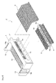
- Figs. 1 through 3 are an upper perspective view, a lower perspective view and an exploded perspective view of a connector C as one embodiment of the present invention.
- the connector C includes a main body 1 formed of an insulator such as resin, a plurality of first contacts 2 fixed in juxtaposition to the main body 1, a plurality of second contacts 3 disposed downwardly of the first contacts 2 and held in juxtaposition to the main body 1, and a contact holder 4 holding and fixing the second contacts 3.
- the connector C is configured to allow selective connection thereto of two different types of connection objects (not shown). When a connection object is connected to the connector C, terminals of the respective connection object come into contact with the first contacts 2 or the second contacts 3. Further, in this embodiment, the number of the second terminals 3 is greater than the number of the first terminals 2.
- the upper and lower sides will be defined based on a reference condition wherein the connector C is placed in a state illustrated in Fig. 1 .
- the side (the left side in Fig. 1 ) on which the connection object is connected to the main body 1 will be defined as the front side.
- the main body 1 includes a base portion 11, a holding portion 12 and side walls 13.
- the holding portion 12 extends forwardly from the front face of the base portion 11.
- the side walls 13 extend forwardly from opposed side portions of the base portion 11 and are formed to sandwich the holding portion 12 from its opposite sides.
- the base portion 11, as shown in Fig. 3 includes, in its back face, a fixing portion 15 for fixing the contact holder 4.
- the fixing portion 15 is provided in the form of an aperture formed at a lower portion of the rear face of the base portion 11 and having a rectangular cross sectional shape and configured to allow engagement of the contact holder 4 into this aperture.
- Grooves 14 are formed to extend from the rear face of the main body 1 to and over the upper face of the holding portion 12.
- Grooves 16 are formed to extend from the front end face of the fixing portion 15 over to the lower face of the holding portion 12.
- the first contacts 12 are held in the grooves 14 and the second contacts 3 are held in the grooves 16 (see Fig. 1, Fig. 2 ).
- each side wall 13 In an end face on the outer side of each side wall 13, a reinforcing terminal 13a is attached.
- This reinforcing terminal 13a has its lower portion bent at a right angle to the outer side. When this portion is fixed to a circuit board or the like by e.g. solder, fixation of the circuit board or the like to the connector C is reinforced.
- the first contact 2 and the second contact 3 respectively have contact portions 2a and 3a which respectively come into contact with corresponding terminals of the two types of unillustrated connection objects and also have tail portions 2b and 3b which respectively are to be fixed to the circuit board or the like by e.g. solder.
- Each of the first contact 2 and the second contact 3 is provided approximately like a bar; and the contact portion 2a has an upwardly convex arch shape whereas the contact portion 3a has a downwardly convex arch shape.
- the contact points 2a, 3a respectively come into contact with and become elastically deformed by the terminals of the two types of connection objects to be connected to the connector C.
- the tail portions 2b, 3b of the first contact 2 and the second contact 3 are formed to be bent along the circuit board or the like to which the connector C is fixed and are fixed to the circuit board or the like by e.g. reflow soldering. With these, the respective connection objects and the circuit board or the like can be electrically connected to each other via the connector C.
- the first contacts 2 and the second contacts 3 are held in the grooves 14 and the grooves 16, respectively.
- each one of these is press-fitted into an individual groove 14 from the rear side of the base portion 11.
- the second contacts 3 are configured such that firstly the second contacts 3 and the contact holder 4 are formed integral with each other and thereafter the contact holder 4 to which the second contacts 3 have been fixed is fixed to the main body 1. In this process, the second contacts 3 will be engaged within the grooves 16.
- the number of the second contacts 3 is greater than the number of the first contacts 2.
- the forming pitch of the grooves 16 is set narrower that that of the grooves 14 (see Fig. 5 ).
- the contacts 3 would be tilted, thus leading to disadvantageous reduction in the flatness of the first contacts 2 and the second contacts 3, in particular, the flatness of their tail portions 2b, 3b. Consequently, there may arise failure to provide fixation with keeping good uniformity of the flatness of the tail portions 2b and the tail portions 3b as a whole.
- narrow pitch requires certain reduction in the thickness of a resin wall configured to provide electrical insulation between adjacent contacts.
- the resin wall is formed thin, even when it is attempted to hold the second contact 2 by press-fitting, it will not be possible to provide the second contact 3 with an amount of press-fitting margin sufficient for ensuring required press-fitting strength for the second contact 3.
- the second contacts 3 are fixed in advance via the contact holder 4 through integral molding and then these are fixed to the main body 1. This arrangement provides not only the possibility of ensuring uniformity in the flatness of the tail portions 2b, 3b, but also the possibility of ensuring sufficient holding strength of the second contact 3 relative to the contact holder 4.
- the contact holder 4 is formed of e.g. resin and has an approximately rectangular parallelepiped shape. And, in the upper and lower faces and the side faces of this contact holder 4, there are respectively provided projecting portions 4a extending from the front end to the rear end of each face. Further, in the upper face of the contact holder 4, there are provided exposing portions 4b formed as through holes having a rectangular cross sectional shape, so that the second contacts 3 are partially exposed therethrough.
- the contact holder 4 and the second contacts 3 are formed integrally by e.g. an insert molding technique. In this way, as the second contacts 3 are fixed in juxtaposition first and then the contact holder 4 is inserted into the fixing portion 15 of the main body 1, the second contacts 3 are caused to be held to the main body 1. With this, even in the case of narrow pitch of contacts, it is still possible to fix the second contacts 3 to the main body 1 in a stable manner. As a result, the tail portions 3b of the second contacts 3 will be provided with uniform flatness, which permits in turn reliable soldering fixation of the tail portions 3b to the circuit board or the like.
- Fig. 5 is a rear view in section showing the connector C according to the instant embodiment.
- the projecting portions 4a provided at multiple portions of this contact holder 4 are fixed as being placed in contact with the inner circumferential face of the fixing portion 15 of the main body 1. Namely, the upper and lower faces and the side faces of the contact holder 4, except for the projecting portions 4a, are kept out of contact from the main body 1.
- the contact holder 4 even if deformation occurs in the main body 1 at the time of reflow heating of the connector C, it is possible to prevent the contact holder 4 from being deformed in suit with such deformation of the main body 1.
- the contact holder 4 incudes the exposing portions 4b formed to cause the second contacts 3 to be partially exposed therethrough (see Fig. 6 ).
- air and a resin have different dielectric constants from each other. Therefore, impedance control is made possible by changing the size or position of this exposing portion 4b for changing the exposed state of the second contact 3.
- forming the exposing portions 4b allows reduction in the volume (amount) of the resin forming the contact holder 4. Thus, it is possible to avoid shrinkage that would otherwise occur at the time of insert molding process.
- the exposing portions 4b are formed as through holes through which the contacts are exposed vertically as provided in the instant embodiment, a mold used for molding these holes at the time of insert molding can sandwich the second contacts 3 vertically for fixing them therebetween. Therefore, this embodiment arrangement is more preferred since it allows prevention of displacement of the contacts due to the flowing pressure of the forming resin.
- the spring constant can be changed as desired by a simple operation of changing the thickness of the contact, thus setting a contact load suitable for a particular use and/or using environment contemplated.
- each second contact 3 the portion thereof covered by the resin of the contact holder 4 has an increased width. With this, it becomes possible to increase the area of second contact 3 to be fixed by the contact holder 4. As a result, the second contact 3 can be held and fixed to the contact holder 4 in a secure manner.
- This disclosure is applicable to a connector having a plurality of contacts.
Landscapes
- Coupling Device And Connection With Printed Circuit (AREA)
- Connector Housings Or Holding Contact Members (AREA)
Abstract
Description
- This disclosure relates to a connector having a plurality of contacts.
- Conventionally, as such a connector described above, there is known one disclosed in Japanese Unexamined Patent Application Publication (Translation of PCT Application) No.
2005-525684 - However, such connector described above, when the number of contacts to be mounted increases, this leads to decrease in the pitch of the grooves to be formed, which decrease will then lead to reduction in the thickness of an amount of resin to be placed between adjacent grooves (a holding margin for contacts). Consequently, there may arise inability of press-fitting the contacts into a main body in a stable manner. Also, due to thermal deformation of the main body at the time of reflow heating, the contacts can be tilted. This causes decrease in the flatness of the contacts and eventual inability for reliable fixation thereof to e.g. a circuit board or the like.
- In addressing to such problems as above, it has been practiced to provide, in an assembly process of contacts, a sizing step or to effect a correcting step through a manual work by a worker. In this case, however, inclusion of such additional step can invite cost increase and/or reduction in production efficiency.
- According to one preferred embodiment of the present invention, there is provided a connector having a plurality of contacts and capable of holding them in alignment with each other.
- According to one preferred embodiment of the present invention, a connector comprises a main body, a plurality of contacts to be electrically connected to a connection object, and a contact holder holding the plurality of contacts in juxtaposition, wherein the main body includes a fixing portion for fixing the contact holder, and the plurality of contacts are fixedly held to the contact holder through integral molding therewith.
- With the above arrangement, after the contacts are fixedly held to the contact holder through integral molding, this contact holder is fixed to the main body. As a result, the main body can hold the contacts, with keeping good juxtaposing alignment thereof. Also, when the main body as holding the contacts is subject to a reflow heating process, it is possible to prevent tilting of the contacts due to thermal deformation of the main body. Further, since the thickness of the respective contact can be changed easily without needing any change in the shape of the main body, it is possible, when needed, to change the thickness of the contact for adjustment of its contacting load.
- According to one preferred embodiment of the present invention, the fixing portion includes an aperture in which the contact holder is engaged, and the contact holder includes a projecting portion which comes into contact with an inner circumferential face of the aperture.
- With the above arrangement, the projecting portion of the contact holder comes into contact with the inner circumferential face to be fixed thereto. Thus, it is possible to reduce the contacting area of the contact holder to the main body. As a result, even if deformation should occur in the main body due to temporary heating at the time of reflow heating process, it will still be possible to prevent the contact holder from being deformed in suit therewith, so that the juxtaposed contacts can be maintained in good alignment.
- According to one preferred embodiment of the present invention, the contact holder includes an exposing portion which exposes at least a portion of the contact.
- With the above arrangement, through adjustment of the size and/or position of the exposing portion, the exposed state of each contact can be changed, so that impedance control is made possible.
-
-
Fig. 1 shows an upper perspective view of a connector according to the present invention, -
Fig. 2 is a lower perspective view of the connector according to the present invention, -
Fig. 3 is an exploded perspective view of the connector according to the present invention, -
Fig. 4 is a side view in section of the connector according to the present invention, -
Fig. 5 is a rear view in section of the connector according to the present invention, and -
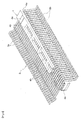
Fig. 6 is a partially cutaway perspective view of a contactor holder provided in the present invention. - Next, embodiments of a connector according to the present invention will be described with reference to the accompanying drawings.
-
Figs. 1 through 3 are an upper perspective view, a lower perspective view and an exploded perspective view of a connector C as one embodiment of the present invention. The connector C includes amain body 1 formed of an insulator such as resin, a plurality offirst contacts 2 fixed in juxtaposition to themain body 1, a plurality ofsecond contacts 3 disposed downwardly of thefirst contacts 2 and held in juxtaposition to themain body 1, and acontact holder 4 holding and fixing thesecond contacts 3. In the instant embodiment, the connector C is configured to allow selective connection thereto of two different types of connection objects (not shown). When a connection object is connected to the connector C, terminals of the respective connection object come into contact with thefirst contacts 2 or thesecond contacts 3. Further, in this embodiment, the number of thesecond terminals 3 is greater than the number of thefirst terminals 2. - Incidentally, in the instant embodiment, the upper and lower sides will be defined based on a reference condition wherein the connector C is placed in a state illustrated in
Fig. 1 . Also, the side (the left side inFig. 1 ) on which the connection object is connected to themain body 1 will be defined as the front side. - The
main body 1 includes abase portion 11, aholding portion 12 andside walls 13. Theholding portion 12 extends forwardly from the front face of thebase portion 11. And, theside walls 13 extend forwardly from opposed side portions of thebase portion 11 and are formed to sandwich theholding portion 12 from its opposite sides. - The
base portion 11, as shown inFig. 3 , includes, in its back face, afixing portion 15 for fixing thecontact holder 4. In this embodiment, thefixing portion 15 is provided in the form of an aperture formed at a lower portion of the rear face of thebase portion 11 and having a rectangular cross sectional shape and configured to allow engagement of thecontact holder 4 into this aperture. -
Grooves 14 are formed to extend from the rear face of themain body 1 to and over the upper face of theholding portion 12.Grooves 16 are formed to extend from the front end face of thefixing portion 15 over to the lower face of theholding portion 12. In this embodiment, thefirst contacts 12 are held in thegrooves 14 and thesecond contacts 3 are held in the grooves 16 (seeFig. 1, Fig. 2 ). - In an end face on the outer side of each
side wall 13, a reinforcingterminal 13a is attached. This reinforcingterminal 13a has its lower portion bent at a right angle to the outer side. When this portion is fixed to a circuit board or the like by e.g. solder, fixation of the circuit board or the like to the connector C is reinforced. - As shown in
Fig. 4 , thefirst contact 2 and thesecond contact 3 respectively havecontact portions tail portions first contact 2 and thesecond contact 3 is provided approximately like a bar; and thecontact portion 2a has an upwardly convex arch shape whereas thecontact portion 3a has a downwardly convex arch shape. With such shapes as above, thecontact points tail portions first contact 2 and thesecond contact 3 are formed to be bent along the circuit board or the like to which the connector C is fixed and are fixed to the circuit board or the like by e.g. reflow soldering. With these, the respective connection objects and the circuit board or the like can be electrically connected to each other via the connector C. - As described above, the
first contacts 2 and thesecond contacts 3 are held in thegrooves 14 and thegrooves 16, respectively. Here, as shown inFig. 3 , for thefirst contacts 2, each one of these is press-fitted into anindividual groove 14 from the rear side of thebase portion 11. Whereas, thesecond contacts 3 are configured such that firstly thesecond contacts 3 and thecontact holder 4 are formed integral with each other and thereafter thecontact holder 4 to which thesecond contacts 3 have been fixed is fixed to themain body 1. In this process, thesecond contacts 3 will be engaged within thegrooves 16. - As described above, the number of the
second contacts 3 is greater than the number of thefirst contacts 2. Thus, the forming pitch of thegrooves 16 is set narrower that that of the grooves 14 (seeFig. 5 ). In the case of such arrangement, if thesecond contacts 3 were directly pressed into thebase portion 11 just like thefirst contacts 2, thecontacts 3 would be tilted, thus leading to disadvantageous reduction in the flatness of thefirst contacts 2 and thesecond contacts 3, in particular, the flatness of theirtail portions tail portions 2b and thetail portions 3b as a whole. - Moreover, narrow pitch requires certain reduction in the thickness of a resin wall configured to provide electrical insulation between adjacent contacts. And, if the resin wall is formed thin, even when it is attempted to hold the
second contact 2 by press-fitting, it will not be possible to provide thesecond contact 3 with an amount of press-fitting margin sufficient for ensuring required press-fitting strength for thesecond contact 3. As a result, it will not be possible to secure sufficient contact holding strength. For this reason, in the instant embodiment, as described above, thesecond contacts 3 are fixed in advance via thecontact holder 4 through integral molding and then these are fixed to themain body 1. This arrangement provides not only the possibility of ensuring uniformity in the flatness of thetail portions second contact 3 relative to thecontact holder 4. - As shown in
Fig. 6 , thecontact holder 4 is formed of e.g. resin and has an approximately rectangular parallelepiped shape. And, in the upper and lower faces and the side faces of thiscontact holder 4, there are respectively provided projectingportions 4a extending from the front end to the rear end of each face. Further, in the upper face of thecontact holder 4, there are provided exposingportions 4b formed as through holes having a rectangular cross sectional shape, so that thesecond contacts 3 are partially exposed therethrough. - The
contact holder 4 and thesecond contacts 3 are formed integrally by e.g. an insert molding technique. In this way, as thesecond contacts 3 are fixed in juxtaposition first and then thecontact holder 4 is inserted into the fixingportion 15 of themain body 1, thesecond contacts 3 are caused to be held to themain body 1. With this, even in the case of narrow pitch of contacts, it is still possible to fix thesecond contacts 3 to themain body 1 in a stable manner. As a result, thetail portions 3b of thesecond contacts 3 will be provided with uniform flatness, which permits in turn reliable soldering fixation of thetail portions 3b to the circuit board or the like. - Moreover, it becomes possible to eliminate such additional steps provided conventionally in the assembly process of the connector, e.g. a sizing step for rendering the flatness of contacts uniform, a correcting step by a manual work. Consequently, it becomes possible to reduce the manufacturing costs.
-
Fig. 5 is a rear view in section showing the connector C according to the instant embodiment. As shown, in the instant embodiment, in thecontact holder 4, the projectingportions 4a provided at multiple portions of thiscontact holder 4 are fixed as being placed in contact with the inner circumferential face of the fixingportion 15 of themain body 1. Namely, the upper and lower faces and the side faces of thecontact holder 4, except for the projectingportions 4a, are kept out of contact from themain body 1. With this arrangement, even if deformation occurs in themain body 1 at the time of reflow heating of the connector C, it is possible to prevent thecontact holder 4 from being deformed in suit with such deformation of themain body 1. Moreover, thanks to the possibility of thickness reduction of the resin except for the projectingportions 4a, it is possible to avoid deformation (shrinkage) due to shrinking of the resin that occurs at the time of insertion molding. Therefore, the flatness of the contacts can be maintained. - As described above, the
contact holder 4 incudes the exposingportions 4b formed to cause thesecond contacts 3 to be partially exposed therethrough (seeFig. 6 ). Generally, air and a resin have different dielectric constants from each other. Therefore, impedance control is made possible by changing the size or position of this exposingportion 4b for changing the exposed state of thesecond contact 3. Further, forming the exposingportions 4b allows reduction in the volume (amount) of the resin forming thecontact holder 4. Thus, it is possible to avoid shrinkage that would otherwise occur at the time of insert molding process. Moreover, if the exposingportions 4b are formed as through holes through which the contacts are exposed vertically as provided in the instant embodiment, a mold used for molding these holes at the time of insert molding can sandwich thesecond contacts 3 vertically for fixing them therebetween. Therefore, this embodiment arrangement is more preferred since it allows prevention of displacement of the contacts due to the flowing pressure of the forming resin. - Furthermore, in the case of an arrangement of press-fitting each individual contact into the
main body 1, it will become necessary to change the shape of themain body 1 if it is desired to change the thickness and/or shape of the contact. Whereas, in the case of the arrangement of the instant embodiment wherein thesecond contacts 3 and thecontact holder 4 are formed integral with each other, it is possible to change the thickness and/or shape of the contact as desired without needing to change the shape of themain body 1. Therefore, the spring constant can be changed as desired by a simple operation of changing the thickness of the contact, thus setting a contact load suitable for a particular use and/or using environment contemplated. - Further, in the instant embodiment, as shown in
Fig. 6 , of eachsecond contact 3, the portion thereof covered by the resin of thecontact holder 4 has an increased width. With this, it becomes possible to increase the area ofsecond contact 3 to be fixed by thecontact holder 4. As a result, thesecond contact 3 can be held and fixed to thecontact holder 4 in a secure manner. -
- (1) In the foregoing embodiment, there was explained the connector C having two kinds of contacts in order to provide connectability to different connection objects. Instead, the connector C can be provided with only one kind of contacts to be connected.
- (2) In the foregoing embodiment, the fixing
portion 15 for fixing thecontact holder 4 is provided in the form of an aperture. However, this can have any desired shape as long as it allows fixation of thecontact holder 4 with multiple contacts formed integral therewith to themain body 1. - (3) In the foregoing embodiment, the
contact holder 4 is provided with the projectingportions 4a. However, these portions can be omitted. - (4) In the foregoing embodiment, the exposing
portions 4b formed in thecontact holder 4 are formed as through holes in thecontact holder 4. However, the specific form of these portions is not particularly limited as long as its allows partial exposure of thesecond contacts 3 therethrough. - (5) In the foregoing embodiment, the
contact holder 4 is provided with the exposingportions 4b. However, these portions can be omitted. - This disclosure is applicable to a connector having a plurality of contacts.
Claims (3)
- A connector comprising:a main body (1);a plurality of contacts (3) to be electrically connected to a connection object; anda contact holder (4) holding the plurality of contacts (3) in juxtaposition;
characterized in that:the main body (1) includes a fixing portion (15) for fixing the contact holder (4); andthe plurality of contacts (3) are fixedly held to the contact holder (4) through integral molding therewith. - The connector according to claim 1, characterized in that:the fixing portion (15) includes an aperture in which the contact holder (4) is engaged, andthe contact holder (4) includes a projecting portion (4a) which comes into contact with an inner circumferential face of the aperture.
- The connector according to claim 1 or 2, characterized in that the contact holder (4) includes an exposing portion (4b) which exposes at least a portion of the contact (3).
Applications Claiming Priority (1)
| Application Number | Priority Date | Filing Date | Title |
|---|---|---|---|
| JP2013119965A JP6142412B2 (en) | 2013-06-06 | 2013-06-06 | connector |
Publications (2)
| Publication Number | Publication Date |
|---|---|
| EP2811579A1 true EP2811579A1 (en) | 2014-12-10 |
| EP2811579B1 EP2811579B1 (en) | 2018-01-17 |
Family
ID=50884690
Family Applications (1)
| Application Number | Title | Priority Date | Filing Date |
|---|---|---|---|
| EP14170272.0A Not-in-force EP2811579B1 (en) | 2013-06-06 | 2014-05-28 | Connector |
Country Status (6)
| Country | Link |
|---|---|
| US (1) | US9548550B2 (en) |
| EP (1) | EP2811579B1 (en) |
| JP (1) | JP6142412B2 (en) |
| KR (1) | KR102165740B1 (en) |
| CN (1) | CN104241914B (en) |
| TW (1) | TWI591903B (en) |
Families Citing this family (3)
| Publication number | Priority date | Publication date | Assignee | Title |
|---|---|---|---|---|
| CN110462941B (en) * | 2017-01-30 | 2022-03-01 | 富加宜(美国)有限责任公司 | Multi-Piece Power Connector with Cable Pass-Through |
| JP6929821B2 (en) | 2018-06-26 | 2021-09-01 | タイコエレクトロニクスジャパン合同会社 | Electrical connector |
| DE102020104022B3 (en) | 2020-02-17 | 2021-08-12 | Md Elektronik Gmbh | Short-circuit pin, plug connection with such a short-circuit pin and a method for producing such a short-circuit pin |
Citations (4)
| Publication number | Priority date | Publication date | Assignee | Title |
|---|---|---|---|---|
| US20040043648A1 (en) * | 2002-08-30 | 2004-03-04 | Houtz Timothy W. | Electrical connector having a cored contact assembly |
| JP2005525684A (en) | 2002-05-10 | 2005-08-25 | モレックス インコーポレーテッド | Edge card connector assembly with terminals with adjusted impedance |
| US20110076894A1 (en) * | 2009-09-30 | 2011-03-31 | Hon Hai Precision Industry Co., Ltd. | Lower profile electrical socket configured with wafers |
| US20120322313A1 (en) * | 2011-06-16 | 2012-12-20 | Hon Hai Precision Industry Co., Ltd. | Receptacle connector having improved contact modules |
Family Cites Families (10)
| Publication number | Priority date | Publication date | Assignee | Title |
|---|---|---|---|---|
| US5200171A (en) * | 1990-11-20 | 1993-04-06 | Micropure, Inc. | Oral health preparation and method |
| US6093061A (en) * | 1998-07-31 | 2000-07-25 | The Whitaker Corporation | Electrical connector having terminal insert subassembly |
| US6200171B1 (en) * | 1999-11-30 | 2001-03-13 | Berg Technology, Inc. | Electrical connector with over-molded housing member and method of over-molding |
| JP2002203626A (en) * | 2000-12-27 | 2002-07-19 | Fujikura Ltd | Connector |
| JP2006515705A (en) | 2002-05-06 | 2006-06-01 | モレックス インコーポレーテッド | Differential signal connector with electrostatic discharge protection function |
| JP2005294036A (en) * | 2004-03-31 | 2005-10-20 | Matsushita Electric Works Ltd | Connector and its manufacturing method |
| JP4385047B2 (en) * | 2006-12-06 | 2009-12-16 | ホシデン株式会社 | Contact and card adapter and card connector provided therewith |
| JP2010212017A (en) * | 2009-03-09 | 2010-09-24 | Japan Aviation Electronics Industry Ltd | Electric connector |
| CN201797100U (en) * | 2010-08-18 | 2011-04-13 | 富士康(昆山)电脑接插件有限公司 | Cable Connector Assembly |
| US8961194B2 (en) * | 2013-03-14 | 2015-02-24 | Bby Solutions, Inc. | Active HDMI connector with integrated design |
-
2013
- 2013-06-06 JP JP2013119965A patent/JP6142412B2/en active Active
-
2014
- 2014-04-18 KR KR1020140046920A patent/KR102165740B1/en active Active
- 2014-04-23 TW TW103114665A patent/TWI591903B/en not_active IP Right Cessation
- 2014-05-28 EP EP14170272.0A patent/EP2811579B1/en not_active Not-in-force
- 2014-06-04 US US14/296,118 patent/US9548550B2/en not_active Expired - Fee Related
- 2014-06-05 CN CN201410246047.6A patent/CN104241914B/en active Active
Patent Citations (4)
| Publication number | Priority date | Publication date | Assignee | Title |
|---|---|---|---|---|
| JP2005525684A (en) | 2002-05-10 | 2005-08-25 | モレックス インコーポレーテッド | Edge card connector assembly with terminals with adjusted impedance |
| US20040043648A1 (en) * | 2002-08-30 | 2004-03-04 | Houtz Timothy W. | Electrical connector having a cored contact assembly |
| US20110076894A1 (en) * | 2009-09-30 | 2011-03-31 | Hon Hai Precision Industry Co., Ltd. | Lower profile electrical socket configured with wafers |
| US20120322313A1 (en) * | 2011-06-16 | 2012-12-20 | Hon Hai Precision Industry Co., Ltd. | Receptacle connector having improved contact modules |
Also Published As
| Publication number | Publication date |
|---|---|
| KR102165740B1 (en) | 2020-10-14 |
| JP2014238939A (en) | 2014-12-18 |
| US9548550B2 (en) | 2017-01-17 |
| JP6142412B2 (en) | 2017-06-07 |
| US20140364011A1 (en) | 2014-12-11 |
| KR20140143319A (en) | 2014-12-16 |
| CN104241914B (en) | 2019-01-25 |
| TW201513481A (en) | 2015-04-01 |
| EP2811579B1 (en) | 2018-01-17 |
| TWI591903B (en) | 2017-07-11 |
| CN104241914A (en) | 2014-12-24 |
Similar Documents
| Publication | Publication Date | Title |
|---|---|---|
| JP6591251B2 (en) | connector | |
| US8454397B2 (en) | Anti-wicking terminal and connector | |
| US11031709B2 (en) | Electrical connector for circuit boards and mounting arrangement for electrical connector for circuit boards | |
| US7435109B1 (en) | Spring connector | |
| JP6600261B2 (en) | Press-fit terminal | |
| US10707619B2 (en) | Movable connector | |
| JP6076952B2 (en) | Board terminal and board with terminal | |
| US9548550B2 (en) | Electrical connector having a plurality of contacts and capable of holding them in alignment | |
| US20220069488A1 (en) | Harness component | |
| JP6815029B2 (en) | Contact, connector member, connector and connected member | |
| US20220045446A1 (en) | Harness component | |
| US20250311087A1 (en) | Continuous flow water heater and heating plate for a continuous flow water heater | |
| KR101625691B1 (en) | Electric connector for circuit substrate | |
| JP6570387B2 (en) | connector | |
| JP2008171627A (en) | Female terminal fitting | |
| US7690928B2 (en) | Plug-in connector | |
| JP6076953B2 (en) | Board terminal | |
| JP2015207353A (en) | Wire connector | |
| EP3595416B1 (en) | Control unit having press-fit structure | |
| JP2019096456A (en) | Chain terminal | |
| US20180151972A1 (en) | Female electrical terminal | |
| JP6010819B2 (en) | Connector board fixing structure | |
| JP2016021330A (en) | Terminal fittings and connectors | |
| JP2022008055A (en) | Terminal | |
| KR102034317B1 (en) | Connector |
Legal Events
| Date | Code | Title | Description |
|---|---|---|---|
| PUAI | Public reference made under article 153(3) epc to a published international application that has entered the european phase |
Free format text: ORIGINAL CODE: 0009012 |
|
| 17P | Request for examination filed |
Effective date: 20140528 |
|
| AK | Designated contracting states |
Kind code of ref document: A1 Designated state(s): AL AT BE BG CH CY CZ DE DK EE ES FI FR GB GR HR HU IE IS IT LI LT LU LV MC MK MT NL NO PL PT RO RS SE SI SK SM TR |
|
| AX | Request for extension of the european patent |
Extension state: BA ME |
|
| R17P | Request for examination filed (corrected) |
Effective date: 20150610 |
|
| RBV | Designated contracting states (corrected) |
Designated state(s): AL AT BE BG CH CY CZ DE DK EE ES FI FR GB GR HR HU IE IS IT LI LT LU LV MC MK MT NL NO PL PT RO RS SE SI SK SM TR |
|
| STAA | Information on the status of an ep patent application or granted ep patent |
Free format text: STATUS: EXAMINATION IS IN PROGRESS |
|
| 17Q | First examination report despatched |
Effective date: 20170125 |
|
| GRAP | Despatch of communication of intention to grant a patent |
Free format text: ORIGINAL CODE: EPIDOSNIGR1 |
|
| STAA | Information on the status of an ep patent application or granted ep patent |
Free format text: STATUS: GRANT OF PATENT IS INTENDED |
|
| RIC1 | Information provided on ipc code assigned before grant |
Ipc: H01R 24/60 20110101ALN20170914BHEP Ipc: H01R 13/405 20060101AFI20170914BHEP Ipc: H01R 13/514 20060101ALI20170914BHEP |
|
| RIC1 | Information provided on ipc code assigned before grant |
Ipc: H01R 13/514 20060101ALI20170921BHEP Ipc: H01R 24/60 20110101ALN20170921BHEP Ipc: H01R 13/405 20060101AFI20170921BHEP |
|
| INTG | Intention to grant announced |
Effective date: 20171002 |
|
| GRAS | Grant fee paid |
Free format text: ORIGINAL CODE: EPIDOSNIGR3 |
|
| GRAA | (expected) grant |
Free format text: ORIGINAL CODE: 0009210 |
|
| STAA | Information on the status of an ep patent application or granted ep patent |
Free format text: STATUS: THE PATENT HAS BEEN GRANTED |
|
| AK | Designated contracting states |
Kind code of ref document: B1 Designated state(s): AL AT BE BG CH CY CZ DE DK EE ES FI FR GB GR HR HU IE IS IT LI LT LU LV MC MK MT NL NO PL PT RO RS SE SI SK SM TR |
|
| REG | Reference to a national code |
Ref country code: GB Ref legal event code: FG4D |
|
| REG | Reference to a national code |
Ref country code: CH Ref legal event code: EP |
|
| REG | Reference to a national code |
Ref country code: IE Ref legal event code: FG4D |
|
| REG | Reference to a national code |
Ref country code: DE Ref legal event code: R096 Ref document number: 602014019982 Country of ref document: DE Ref country code: AT Ref legal event code: REF Ref document number: 965021 Country of ref document: AT Kind code of ref document: T Effective date: 20180215 |
|
| REG | Reference to a national code |
Ref country code: FR Ref legal event code: PLFP Year of fee payment: 5 |
|
| REG | Reference to a national code |
Ref country code: NL Ref legal event code: MP Effective date: 20180117 |
|
| REG | Reference to a national code |
Ref country code: LT Ref legal event code: MG4D |
|
| REG | Reference to a national code |
Ref country code: AT Ref legal event code: MK05 Ref document number: 965021 Country of ref document: AT Kind code of ref document: T Effective date: 20180117 |
|
| PG25 | Lapsed in a contracting state [announced via postgrant information from national office to epo] |
Ref country code: NL Free format text: LAPSE BECAUSE OF FAILURE TO SUBMIT A TRANSLATION OF THE DESCRIPTION OR TO PAY THE FEE WITHIN THE PRESCRIBED TIME-LIMIT Effective date: 20180117 |
|
| PG25 | Lapsed in a contracting state [announced via postgrant information from national office to epo] |
Ref country code: LT Free format text: LAPSE BECAUSE OF FAILURE TO SUBMIT A TRANSLATION OF THE DESCRIPTION OR TO PAY THE FEE WITHIN THE PRESCRIBED TIME-LIMIT Effective date: 20180117 Ref country code: CY Free format text: LAPSE BECAUSE OF FAILURE TO SUBMIT A TRANSLATION OF THE DESCRIPTION OR TO PAY THE FEE WITHIN THE PRESCRIBED TIME-LIMIT Effective date: 20180117 Ref country code: HR Free format text: LAPSE BECAUSE OF FAILURE TO SUBMIT A TRANSLATION OF THE DESCRIPTION OR TO PAY THE FEE WITHIN THE PRESCRIBED TIME-LIMIT Effective date: 20180117 Ref country code: NO Free format text: LAPSE BECAUSE OF FAILURE TO SUBMIT A TRANSLATION OF THE DESCRIPTION OR TO PAY THE FEE WITHIN THE PRESCRIBED TIME-LIMIT Effective date: 20180417 Ref country code: FI Free format text: LAPSE BECAUSE OF FAILURE TO SUBMIT A TRANSLATION OF THE DESCRIPTION OR TO PAY THE FEE WITHIN THE PRESCRIBED TIME-LIMIT Effective date: 20180117 Ref country code: ES Free format text: LAPSE BECAUSE OF FAILURE TO SUBMIT A TRANSLATION OF THE DESCRIPTION OR TO PAY THE FEE WITHIN THE PRESCRIBED TIME-LIMIT Effective date: 20180117 |
|
| PG25 | Lapsed in a contracting state [announced via postgrant information from national office to epo] |
Ref country code: RS Free format text: LAPSE BECAUSE OF FAILURE TO SUBMIT A TRANSLATION OF THE DESCRIPTION OR TO PAY THE FEE WITHIN THE PRESCRIBED TIME-LIMIT Effective date: 20180117 Ref country code: AT Free format text: LAPSE BECAUSE OF FAILURE TO SUBMIT A TRANSLATION OF THE DESCRIPTION OR TO PAY THE FEE WITHIN THE PRESCRIBED TIME-LIMIT Effective date: 20180117 Ref country code: PL Free format text: LAPSE BECAUSE OF FAILURE TO SUBMIT A TRANSLATION OF THE DESCRIPTION OR TO PAY THE FEE WITHIN THE PRESCRIBED TIME-LIMIT Effective date: 20180117 Ref country code: GR Free format text: LAPSE BECAUSE OF FAILURE TO SUBMIT A TRANSLATION OF THE DESCRIPTION OR TO PAY THE FEE WITHIN THE PRESCRIBED TIME-LIMIT Effective date: 20180418 Ref country code: BG Free format text: LAPSE BECAUSE OF FAILURE TO SUBMIT A TRANSLATION OF THE DESCRIPTION OR TO PAY THE FEE WITHIN THE PRESCRIBED TIME-LIMIT Effective date: 20180417 Ref country code: SE Free format text: LAPSE BECAUSE OF FAILURE TO SUBMIT A TRANSLATION OF THE DESCRIPTION OR TO PAY THE FEE WITHIN THE PRESCRIBED TIME-LIMIT Effective date: 20180117 Ref country code: LV Free format text: LAPSE BECAUSE OF FAILURE TO SUBMIT A TRANSLATION OF THE DESCRIPTION OR TO PAY THE FEE WITHIN THE PRESCRIBED TIME-LIMIT Effective date: 20180117 Ref country code: IS Free format text: LAPSE BECAUSE OF FAILURE TO SUBMIT A TRANSLATION OF THE DESCRIPTION OR TO PAY THE FEE WITHIN THE PRESCRIBED TIME-LIMIT Effective date: 20180517 |
|
| REG | Reference to a national code |
Ref country code: DE Ref legal event code: R097 Ref document number: 602014019982 Country of ref document: DE |
|
| PG25 | Lapsed in a contracting state [announced via postgrant information from national office to epo] |
Ref country code: AL Free format text: LAPSE BECAUSE OF FAILURE TO SUBMIT A TRANSLATION OF THE DESCRIPTION OR TO PAY THE FEE WITHIN THE PRESCRIBED TIME-LIMIT Effective date: 20180117 Ref country code: IT Free format text: LAPSE BECAUSE OF FAILURE TO SUBMIT A TRANSLATION OF THE DESCRIPTION OR TO PAY THE FEE WITHIN THE PRESCRIBED TIME-LIMIT Effective date: 20180117 Ref country code: EE Free format text: LAPSE BECAUSE OF FAILURE TO SUBMIT A TRANSLATION OF THE DESCRIPTION OR TO PAY THE FEE WITHIN THE PRESCRIBED TIME-LIMIT Effective date: 20180117 Ref country code: RO Free format text: LAPSE BECAUSE OF FAILURE TO SUBMIT A TRANSLATION OF THE DESCRIPTION OR TO PAY THE FEE WITHIN THE PRESCRIBED TIME-LIMIT Effective date: 20180117 |
|
| PLBE | No opposition filed within time limit |
Free format text: ORIGINAL CODE: 0009261 |
|
| STAA | Information on the status of an ep patent application or granted ep patent |
Free format text: STATUS: NO OPPOSITION FILED WITHIN TIME LIMIT |
|
| PG25 | Lapsed in a contracting state [announced via postgrant information from national office to epo] |
Ref country code: SK Free format text: LAPSE BECAUSE OF FAILURE TO SUBMIT A TRANSLATION OF THE DESCRIPTION OR TO PAY THE FEE WITHIN THE PRESCRIBED TIME-LIMIT Effective date: 20180117 Ref country code: CZ Free format text: LAPSE BECAUSE OF FAILURE TO SUBMIT A TRANSLATION OF THE DESCRIPTION OR TO PAY THE FEE WITHIN THE PRESCRIBED TIME-LIMIT Effective date: 20180117 Ref country code: DK Free format text: LAPSE BECAUSE OF FAILURE TO SUBMIT A TRANSLATION OF THE DESCRIPTION OR TO PAY THE FEE WITHIN THE PRESCRIBED TIME-LIMIT Effective date: 20180117 Ref country code: SM Free format text: LAPSE BECAUSE OF FAILURE TO SUBMIT A TRANSLATION OF THE DESCRIPTION OR TO PAY THE FEE WITHIN THE PRESCRIBED TIME-LIMIT Effective date: 20180117 |
|
| REG | Reference to a national code |
Ref country code: CH Ref legal event code: PL |
|
| 26N | No opposition filed |
Effective date: 20181018 |
|
| REG | Reference to a national code |
Ref country code: BE Ref legal event code: MM Effective date: 20180531 |
|
| PG25 | Lapsed in a contracting state [announced via postgrant information from national office to epo] |
Ref country code: MC Free format text: LAPSE BECAUSE OF FAILURE TO SUBMIT A TRANSLATION OF THE DESCRIPTION OR TO PAY THE FEE WITHIN THE PRESCRIBED TIME-LIMIT Effective date: 20180117 |
|
| REG | Reference to a national code |
Ref country code: IE Ref legal event code: MM4A |
|
| PG25 | Lapsed in a contracting state [announced via postgrant information from national office to epo] |
Ref country code: SI Free format text: LAPSE BECAUSE OF FAILURE TO SUBMIT A TRANSLATION OF THE DESCRIPTION OR TO PAY THE FEE WITHIN THE PRESCRIBED TIME-LIMIT Effective date: 20180117 Ref country code: LI Free format text: LAPSE BECAUSE OF NON-PAYMENT OF DUE FEES Effective date: 20180531 Ref country code: CH Free format text: LAPSE BECAUSE OF NON-PAYMENT OF DUE FEES Effective date: 20180531 |
|
| PG25 | Lapsed in a contracting state [announced via postgrant information from national office to epo] |
Ref country code: LU Free format text: LAPSE BECAUSE OF NON-PAYMENT OF DUE FEES Effective date: 20180528 |
|
| PG25 | Lapsed in a contracting state [announced via postgrant information from national office to epo] |
Ref country code: IE Free format text: LAPSE BECAUSE OF NON-PAYMENT OF DUE FEES Effective date: 20180528 |
|
| PG25 | Lapsed in a contracting state [announced via postgrant information from national office to epo] |
Ref country code: BE Free format text: LAPSE BECAUSE OF NON-PAYMENT OF DUE FEES Effective date: 20180531 |
|
| PG25 | Lapsed in a contracting state [announced via postgrant information from national office to epo] |
Ref country code: MT Free format text: LAPSE BECAUSE OF NON-PAYMENT OF DUE FEES Effective date: 20180528 |
|
| PG25 | Lapsed in a contracting state [announced via postgrant information from national office to epo] |
Ref country code: TR Free format text: LAPSE BECAUSE OF FAILURE TO SUBMIT A TRANSLATION OF THE DESCRIPTION OR TO PAY THE FEE WITHIN THE PRESCRIBED TIME-LIMIT Effective date: 20180117 |
|
| PG25 | Lapsed in a contracting state [announced via postgrant information from national office to epo] |
Ref country code: HU Free format text: LAPSE BECAUSE OF FAILURE TO SUBMIT A TRANSLATION OF THE DESCRIPTION OR TO PAY THE FEE WITHIN THE PRESCRIBED TIME-LIMIT; INVALID AB INITIO Effective date: 20140528 Ref country code: PT Free format text: LAPSE BECAUSE OF FAILURE TO SUBMIT A TRANSLATION OF THE DESCRIPTION OR TO PAY THE FEE WITHIN THE PRESCRIBED TIME-LIMIT Effective date: 20180117 |
|
| PG25 | Lapsed in a contracting state [announced via postgrant information from national office to epo] |
Ref country code: MK Free format text: LAPSE BECAUSE OF NON-PAYMENT OF DUE FEES Effective date: 20180117 |
|
| PGFP | Annual fee paid to national office [announced via postgrant information from national office to epo] |
Ref country code: GB Payment date: 20240522 Year of fee payment: 11 |
|
| PGFP | Annual fee paid to national office [announced via postgrant information from national office to epo] |
Ref country code: DE Payment date: 20240426 Year of fee payment: 11 |
|
| PGFP | Annual fee paid to national office [announced via postgrant information from national office to epo] |
Ref country code: FR Payment date: 20240516 Year of fee payment: 11 |
|
| REG | Reference to a national code |
Ref country code: DE Ref legal event code: R119 Ref document number: 602014019982 Country of ref document: DE |
|
| GBPC | Gb: european patent ceased through non-payment of renewal fee |
Effective date: 20250528 |
|
| PG25 | Lapsed in a contracting state [announced via postgrant information from national office to epo] |
Ref country code: GB Free format text: LAPSE BECAUSE OF NON-PAYMENT OF DUE FEES Effective date: 20250528 |
|
| PG25 | Lapsed in a contracting state [announced via postgrant information from national office to epo] |
Ref country code: DE Free format text: LAPSE BECAUSE OF NON-PAYMENT OF DUE FEES Effective date: 20251202 |
|
| PG25 | Lapsed in a contracting state [announced via postgrant information from national office to epo] |
Ref country code: FR Free format text: LAPSE BECAUSE OF NON-PAYMENT OF DUE FEES Effective date: 20250531 |