EP2810372B1 - Apparatus and method for generating interleaver index - Google Patents
Apparatus and method for generating interleaver index Download PDFInfo
- Publication number
- EP2810372B1 EP2810372B1 EP12867539.4A EP12867539A EP2810372B1 EP 2810372 B1 EP2810372 B1 EP 2810372B1 EP 12867539 A EP12867539 A EP 12867539A EP 2810372 B1 EP2810372 B1 EP 2810372B1
- Authority
- EP
- European Patent Office
- Prior art keywords
- adder
- result
- index
- input
- multiplexer
- Prior art date
- Legal status (The legal status is an assumption and is not a legal conclusion. Google has not performed a legal analysis and makes no representation as to the accuracy of the status listed.)
- Active
Links
Images


Classifications
-
- H—ELECTRICITY
- H03—ELECTRONIC CIRCUITRY
- H03M—CODING; DECODING; CODE CONVERSION IN GENERAL
- H03M13/00—Coding, decoding or code conversion, for error detection or error correction; Coding theory basic assumptions; Coding bounds; Error probability evaluation methods; Channel models; Simulation or testing of codes
- H03M13/27—Coding, decoding or code conversion, for error detection or error correction; Coding theory basic assumptions; Coding bounds; Error probability evaluation methods; Channel models; Simulation or testing of codes using interleaving techniques
-
- H—ELECTRICITY
- H03—ELECTRONIC CIRCUITRY
- H03M—CODING; DECODING; CODE CONVERSION IN GENERAL
- H03M13/00—Coding, decoding or code conversion, for error detection or error correction; Coding theory basic assumptions; Coding bounds; Error probability evaluation methods; Channel models; Simulation or testing of codes
- H03M13/27—Coding, decoding or code conversion, for error detection or error correction; Coding theory basic assumptions; Coding bounds; Error probability evaluation methods; Channel models; Simulation or testing of codes using interleaving techniques
- H03M13/2771—Internal interleaver for turbo codes
-
- H—ELECTRICITY
- H03—ELECTRONIC CIRCUITRY
- H03M—CODING; DECODING; CODE CONVERSION IN GENERAL
- H03M13/00—Coding, decoding or code conversion, for error detection or error correction; Coding theory basic assumptions; Coding bounds; Error probability evaluation methods; Channel models; Simulation or testing of codes
- H03M13/27—Coding, decoding or code conversion, for error detection or error correction; Coding theory basic assumptions; Coding bounds; Error probability evaluation methods; Channel models; Simulation or testing of codes using interleaving techniques
- H03M13/2739—Permutation polynomial interleaver, e.g. quadratic permutation polynomial [QPP] interleaver and quadratic congruence interleaver
-
- H—ELECTRICITY
- H03—ELECTRONIC CIRCUITRY
- H03M—CODING; DECODING; CODE CONVERSION IN GENERAL
- H03M13/00—Coding, decoding or code conversion, for error detection or error correction; Coding theory basic assumptions; Coding bounds; Error probability evaluation methods; Channel models; Simulation or testing of codes
- H03M13/27—Coding, decoding or code conversion, for error detection or error correction; Coding theory basic assumptions; Coding bounds; Error probability evaluation methods; Channel models; Simulation or testing of codes using interleaving techniques
- H03M13/276—Interleaving address generation
-
- H—ELECTRICITY
- H03—ELECTRONIC CIRCUITRY
- H03M—CODING; DECODING; CODE CONVERSION IN GENERAL
- H03M13/00—Coding, decoding or code conversion, for error detection or error correction; Coding theory basic assumptions; Coding bounds; Error probability evaluation methods; Channel models; Simulation or testing of codes
- H03M13/65—Purpose and implementation aspects
- H03M13/6561—Parallelized implementations
-
- H—ELECTRICITY
- H03—ELECTRONIC CIRCUITRY
- H03M—CODING; DECODING; CODE CONVERSION IN GENERAL
- H03M13/00—Coding, decoding or code conversion, for error detection or error correction; Coding theory basic assumptions; Coding bounds; Error probability evaluation methods; Channel models; Simulation or testing of codes
- H03M13/37—Decoding methods or techniques, not specific to the particular type of coding provided for in groups H03M13/03 - H03M13/35
- H03M13/39—Sequence estimation, i.e. using statistical methods for the reconstruction of the original codes
- H03M13/395—Sequence estimation, i.e. using statistical methods for the reconstruction of the original codes using a collapsed trellis, e.g. M-step algorithm, radix-n architectures with n>2
Definitions
- the present invention relates to an apparatus and a method for generating an interleaver index, and more particularly to an apparatus and a method for generating an internal interleaver index of a turbo encoder in parallel.
- indexes of an input stream and an output stream follow the below equation.
- ⁇ i f 1 * i + f 2 * i 2 mod ⁇ K
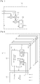
- FIG. 1 is a diagram illustrating an apparatus 100 for generating an internal interleaver index of a conventional turbo encoder.
- the apparatus 100 for generating the internal interleaver index of the conventional turbo encoder includes a first multiplier 110, an adder 120, a second multiplier, and a divider 140.
- the first multiplier 110 receives inputs of f 2 and i and outputs a value of f 2 *i.
- the adder 120 receives inputs of i and f 2 *i output through the first multiplier 110 and outputs a value of f 2 *i+f 1 .
- the second multiplier 130 receives inputs of i and f 2 *i+f 1 output through the adder 120 and outputs a value of (f 2 *i+f 1 )*i.
- the divider 140 receives inputs of K and (f 2 *i+f 1 )*i, performs (f 2 *i+f 1 )*i/K, and then outputs (f 2 *i+f 1 ) *imodK corresponding to the remainder.
- the apparatus 100 for generating the internal interleaver index of the conventional turbo encoder outputs the index in the unit of bits, so that the time for generating the index is increased in proportion to the size of the input data. As a result, the performance of the apparatus is deteriorated.
- the apparatus 100 for generating the internal interleaver index of the conventional turbo encoder requires the multiplier and the divider, which have high importance in an aspect of the hardware implementation, in order to generate the index.
- An aspect of the present invention provides an apparatus and a method for generating an interleaver index, which calculates indexes for following bits by using an index value extracted for a predetermined bit of input data while generating interleaver indexes for a plurality of bits in parallel.
- an apparatus configured for generating indexes of an interleaver for input data, the apparatus including a main processor for calculating an index for a predetermined bit of the input data; and an index operator for receiving the index calculated by the main processor, calculating in parallel indexes for bits after the predetermined bit, and deriving a plurality of indexes.
- the main processor or the index operator may calculate the index by using a difference between indexes.
- a modular operation may be performed using an addition and a multiplexer.
- the addition may be an addition of a dividend and a sign inverted divisor of the modular operation, and the multiplexer may receive inputs of a result of the addition and the dividend, wherein the multiplexer may output the dividend when the result of the addition is a negative number and output the result of the addition when the result of the addition is a positive number.
- the main processor may calculate indexes for i th to i+15 th bits (i is an integer equal to or larger than 0) of the input data, and the index operator may calculate an index for an (i+j)+16 th bit (0 ⁇ j ⁇ 7) by using a difference between i+j th and (i+j)+8 th bits.
- the modular operation may be performed using a first addition, a second addition, and a multiplexer through receptions of a first input, a second input, and a divisor of K.
- the first addition may be an addition of the first input and a sign inverted second input
- the second addition may be an addition of a result of the first addition and a divisor of K
- the multiplexer receives inputs of the result of the first addition and a result of the second addition and outputs the result of the second addition when the result of the first addition is a negative number and outputs the result of the first addition when the result of the first addition is a positive number.
- a method of generating indexes of an interleaver for input data including performing a first step by calculating an index for a predetermined bit of the input data; and performing a second step by calculating indexes for bits after the predetermined bit in parallel by using the calculated index.
- a modular operation may be performed using an addition and a multiplexer, wherein the addition may be an addition of a dividend and a sign inverted divisor of the modular operation, and the multiplexer may receive inputs of a result of the addition and the dividend, wherein the multiplexer may output the dividend when the result of the addition is a negative number and output the result of the addition when the result of the addition is a positive number.
- the addition may be an addition of a dividend and a sign inverted divisor of the modular operation
- the multiplexer may receive inputs of a result of the addition and the dividend, wherein the multiplexer may output the dividend when the result of the addition is a negative number and output the result of the addition when the result of the addition is a positive number.
- the modular operation may be performed using a first addition, a second addition, and a multiplexer through receptions of a first input, a second input, and a divisor of K, wherein the first addition may be an addition of the first input and a sign inverted second input, the second addition may be an addition of a result of the first addition and the divisor of K, and the multiplexer may receive inputs of the result of the first addition and a result of the second addition and output the result of the second addition when the result of the first addition is a negative number and output the result of the first addition when the result of the first addition is a positive number.
- the present invention has an effect of reducing the time spent for generating total indexes by generating indexes for a plurality of bits in parallel.
- the present invention has an effect of improving the resource efficiency and the performance in the hardware implementation by calculating indexes for following bits through the use of an index calculated for a predetermined bit without the use of a multiplier and a divider.
- FIG. 2 is a diagram illustrating an interleaver index generating apparatus 200 according to an embodiment of the present invention.
- the interleaver index generating apparatus 200 includes a main processor 210 and eight index operators 220.
- Each of the index operators 220 includes a first storage apparatus 221, a second storage apparatus 222, and a subsequent-index generator 223.
- the interleaver index generating apparatus 200 generates indexes of the interleaver for input data.
- the main processor 210 calculates an index for a predetermined bit of input data.
- the main processor 210 calculates an index for a predetermined bit of input data by using the difference between index values.
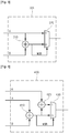
- FIG. 3 is a diagram illustrating a modular circuit 300 according to an embodiment of the present invention.
- the modular circuit 300 according to the embodiment of the present invention includes an adder 310 and a multiplexer 320.
- a modular operation corresponds to an operation for outputting a remainder generated by multiplying a dividend by a divisor.
- the adder 310 receives inputs of the dividend and the divisor and adds the dividend and a sign inverted divisor. That is, the adder 310 derives a value generated by subtracting the divisor from the dividend.
- the multiplexer 320 receives inputs of a result of the addition and the dividend.
- the multiplexer outputs the dividend when the result of the addition is a negative number and outputs the result of the addition when the result of the addition is a positive number.
- the index for the predetermined bit is operated through the modular operation using the modular circuit 300 according to an embodiment of the present invention.
- the main processor 210 does not provide the index operator 220 with the index value for the predetermined bit
- the index for the predetermined bit may be operated through the modular circuit 300 according to the embodiment of the present invention and then the operated index may be provided to the index operator 220.
- the modular circuit 300 has an effect of replacing the multiplier and the divider with the multiplexer and the adder, which are less important resources in an aspect of the hardware implementation.
- the modular operation has an effect of managing efficient hardware resources through the replacement of the divider with the adder and the multiplexer, which are circuit elements having less importance in an aspect of the hardware implementation.
- FIG. 5 is a diagram illustrating an interleaver index generating apparatus 500 according to another embodiment of the present invention.
- the interleaver index generating apparatus 500 includes three adders 511, 512, and 513, two multiplexers 521 and 522, two D-flip flops 531 and 532, and three modular operators 541, 542, and 543.
- the interleaver index generating apparatus 500 receives inputs of (f 1 +f 2 )modK, (2*f 2 )modK, and K and sequentially outputs II(i).
- the first adder 511 receives an input of (2*f 2 )modK and outputs a result value of the addition of (2*f 2 )modK and an output value of the first modular operator 541. In an initial performance, it is not possible to receive the output value of the first modular operator 541 so the output value of the first adder 511 is in an unknown state.
- the first multiplexer 521 receives inputs of the output value of the first adder 511 and "0", outputs "0" in generating a first index by a control signal, and then outputs the output value of the first adder 511 after that.
- the reason why "0" is generated as the first index is that a first index of the interleaver should be "0" and also a first output value of the first adder 511 is in an unknown state.
- the first D-flip flop 531 receives an input of the output value of the first multiplexer 521 and temporarily stores the output value of the first multiplexer 521 because a loop-back is performed in which an output value of the first modular operator 541 is used in the first adder 511.
- the first modular operator 541 receives inputs of K and the output value of the first D-flip flop 531 and performs the modular operation described through FIG. 3 .
- the second adder 512 outputs a result of the addition of the output value of the first modular operator 541 and (f 1 +f 2 )modK.
- the second modular operator 542 receives inputs of K and the output value of the second adder 512 and performs the modular operation described through FIG. 3 .
- the third adder 513 receives an input of the output value of the second modular operator 542 and outputs a result of the addition of the output value of the second modular operator 542 and the output value of the second D-flip flop 532. In an initial performance, it is not possible to receive the output value of the second D-flip flop 532 so the output value is in an unknown state.
- the third modular operator 543 receives inputs of K and the output value of the third adder 513 and performs the modular operation described through FIG. 3 .
- the second multiplexer 522 receives inputs of the output value of the third modular operator 543 and "0", outputs "0" in generating a first index by a control signal, and then outputs the output value of the third adder 543 after that.
- the reason why "0" is generated as the first index is that a first index of the interleaver should be "0" and also a first output value of the third adder 543 is in an unknown state.
- the second D-flip flop 532 receives an input of the output value of the second multiplexer 522 and temporarily stores the output value of the second multiplexer 522 because a loop-back is performed in which the output value of the second multiplexer 522 is used in the third adder 513.
- the interleaver index generating apparatus 500 may be used for deriving an index value for a predetermined bit provided to the index operator 220 from the main processor 210. That is, when the main processor 210 does not provide the index operator 220 with the index value for the predetermined bit, the index for the predetermined bit is operated using the interleaver index generating apparatus 500 and then the operated index may be provided to the index operator 220.
- the main processor 210 calculates (128*f 2 )modK and indexes for i th to i+15 th bits (here, i is an integer equal to or larger than 0) of input data and transfers them to the index operator 220.
- the main processor 210 transfers K, (128*f 2 )modK, and index values for i+j th and (i+j)+8 th bits (here, 0 ⁇ j ⁇ 7) of input data to each of the eight index operators 220.
- the index operator 220 calculates indexes for bits after bits calculated by the main processor 210 in parallel by using the values transferred from the main processor 210 and derives a plurality of indexes.
- the index operator 220 receives index values for i+j th and (i+j)+8 th bits (here, 0 ⁇ j ⁇ 7) of input data from the main processor 210 and calculates an index for an (i+j)+16 th bit by using the difference between the indexes.
- the index value for the i+j th bit of the input data is represented as II(i 0 )
- the index value for the (i+j)+8 th bit of the input data is represented as II(i 1 ).
- i is represented as i m in which i is increased by 8. That is, i m+1 is equal to i m +8 and i m+2 is equal to i m +16.
- the index of the interleaver has the following characteristics.
- the index generator 220 includes the first storage apparatus 221, the second storage apparatus 222, and the subsequent-index generator 223.
- the index generator 220 receives ⁇ (i 0 ), ⁇ (i 1 ), (128*f 2 )modK, and K from the main processor 210, calculates indexes after II(i 0 ), and enables outputs to be sequentially output from II(i 0 ).
- the first storage apparatus 221 receives II(i 0 ) from the main processor 210 and stores the received II(i 0 ) at first. After that, the first storage apparatus 221 sequentially receives II(i m+1 ) stored in the second storage apparatus 222 and stores the received II(i m+1 ). Further, the first storage apparatus 221 transfers stored values to the subsequent-index generator 223. And then the first storage apparatus 221 sequentially outputs stored values as output values of the index operator 220.
- the first storage apparatus 221 stores and outputs first II(i 0 ), the second storage apparatus 222 receives the first stored II(i 1 ) and then stores and outputs the received II(i 1 ), and then the second storage apparatus 222 receives II(i 2 ) output through II(i 0 ) and II(i 1 ) by the subsequent-index generator 223 and then stores and outputs the received II(i 2 ). That is, the first storage apparatus 221 sequentially stores values from II(i 0 ) to II(i m ), transfers them to the subsequent-index generator 223, and outputs them as output values of the index operator 220.
- the second storage apparatus 222 receives II(i 1 ) from the main processor 210 and stores the received II(i 1 ). After that, the second storage apparatus 222 receives II(i m+2 ), which is an output value of the subsequent-index generator 223, and stores the received II(i m+2 ). Further, the second storage apparatus 222 transfers stored values to the subsequent-index generator 223 and the first storage apparatus 221. That is, the second storage apparatus 222 sequentially stores values from II(i 1 ) to II(i m+1 ) and transfers them to the subsequent-index generator 223 and the first storage apparatus 221.
- index operators 220 there are eight index operators 220 and the eight index operators receive ( ⁇ (0), ⁇ (8)), ( ⁇ (1), ⁇ (9)), ( ⁇ (2), ⁇ (10)), ( ⁇ (3), ⁇ (11)), ( ⁇ (4), ⁇ (12)), ( ⁇ (5), ⁇ (13)), ( ⁇ (6), ⁇ (14)), ( ⁇ (7), ⁇ (15)) to output ⁇ (n*8), ⁇ (n*8+1), ⁇ (n*8+2), ⁇ (n*8+3), ⁇ (n*8+4), ⁇ (n*8+5), ⁇ (n*8+6), ⁇ (n*8+7), respectively (n is an integer equal to or larger than 2 and equal to or smaller than (K/8-1)).
- FIG. 4 is a diagram illustrating a modular circuit 400 according to another embodiment of the present invention.
- the modular circuit 400 according to another embodiment of the present invention includes a first adder 410, a second adder 420, and a multiplexer 430 and receives a first input, a second input, and a divisor K.
- the first adder 410 adds the first input and a sign inverted second input and outputs the added value. That is, the first adder 410 subtracts the second input from the first input.
- the second adder 420 adds the output value of the first adder 410 and the divisor K and outputs the added value.
- the multiplexer 430 receives inputs of the output value of the first adder 410 and the output value of the second adder 420.
- the multiplexer outputs the output value of the first adder 410 when the output value of the first adder 410 is a positive number and outputs the output value of the second adder 420 when the output value of the first adder 410 is a negative number.
- FIG. 6 is a diagram illustrating a subsequent-index generator according to an embodiment of the present invention.
- the subsequent-index generator 600 according to the embodiment of the present invention includes two modular operators 610 and 620 described through FIG. 3 , one modular operator 630 described through FIG. 4 , and one adder 640.
- the subsequent-index generator 600 receives inputs of (128*f 2 )modK, 2*II(i m ), K, and II(i m+1 ) and outputs II(i m+2 ).
- 2*II(i m ) received by the subsequent-index generator 600 according to the embodiment of the present invention may be operated by applying a bit shift through a reception of II(i m ) without the use of multiplier.
- the first modular operator 610 receives inputs of 2*II(i m ) and K, and performs the modular operation described in FIG. 3 .
- the second modular operator 630 receives inputs of the output value of the first modular operator 610, II(i m+1 ), and K, and performs the modular operation described in FIG. 4 .
- the adder 640 adds the output value of the second modular operator 630 and (128*f 2 )modK and outputs the added value.
- the third modular operator 620 receives inputs of the output value of the adder 640 and K, and performs the modular operation described in FIG. 3 .
- the output value of the third modular operator 620 corresponds to the output value of the subsequent-index generator 600, which is II(i m+2 ).
- the aforementioned multiplexer can determine whether an input value is a negative number or a positive number by using a most significant bit value.
- FIG. 7 is a flowchart illustrating an interleaver index generating method according to an embodiment of the present invention.
- the interleaver index generating method according to the embodiment of the present invention includes calculating K, f 1 , and f 2 from input data in step S710, calculating values of indexes from II(i) to II(i+15) for i th to i+15 th bits, which are predetermined bits of the input data, by using the K, f 1 , and f 2 calculated in step S710 in step S720, and calculating in parallel values from II(i+16) by using the values from II(i) to II(i+15) calculated in step S720 and differences between the index values in step S730.
- step S710 the index generating apparatus calculates K, f 1 , and f 2 from input data.
- step S720 the index generating apparatus calculates indexes for predetermined bits of the input data by using K, f 1 , and f 2 calculated in step S710.
- the modular operation is performed using an addition and the multiplexer.
- the addition refers to an addition of the dividend and the sign inverted divisor of the modular operation
- the multiplexer receives inputs of a result of the addition and the dividend.
- the multiplexer outputs the dividend when the result of the addition is a negative number and outputs the result of the addition when the result of the addition is a positive number.
- the index generating apparatus calculates indexes for i th to i+15 th bits (here, i is an integer equal to or larger than 0) of input data and (128*f 2 )modK in step S720.
- step S730 the index generating apparatus calculates in parallel indexes for bits after the bit calculated using the index values calculated in step S720.
- the index generating apparatus receives a first input, a second input, and an input of the divisor K, and uses the modular operation performed using a first addition, a second addition, and the multiplexer in step S730.
- Each of the operations used in the modular operation is as follows.
- the first addition refers to an addition of the first input and a sign inverted second input
- the second addition refers to an addition of a result of the first addition and the divisor K.
- the multiplexer receives inputs of the result of the first addition and a result of the second addition.
Landscapes
- Physics & Mathematics (AREA)
- Probability & Statistics with Applications (AREA)
- Engineering & Computer Science (AREA)
- Theoretical Computer Science (AREA)
- Mathematical Physics (AREA)
- Error Detection And Correction (AREA)
Description
- The present invention relates to an apparatus and a method for generating an interleaver index, and more particularly to an apparatus and a method for generating an internal interleaver index of a turbo encoder in parallel.
- In general, the relation between an input and an output of an internal interleaver of a turbo encoder follows the below equation when inputs are C 0,C 1,C 2,...C k-1 and outputs are C' 0, C' 1, C' 2,...C' k-1.

- Further, indexes of an input stream and an output stream follow the below equation.

-
FIG. 1 is a diagram illustrating anapparatus 100 for generating an internal interleaver index of a conventional turbo encoder. - Referring to
FIG. 1 , theapparatus 100 for generating the internal interleaver index of the conventional turbo encoder includes afirst multiplier 110, anadder 120, a second multiplier, and adivider 140. - The
apparatus 100 for generating the internal interleaver index of the conventional turbo encoder receives inputs of K, which is a size of input data, f1 and f2 calculated from K, and a value of i according to an order of bits and outputs II(i) satisfying
- The
first multiplier 110 receives inputs of f2 and i and outputs a value of f2*i. - The
adder 120 receives inputs of i and f2*i output through thefirst multiplier 110 and outputs a value of f2*i+f1. - The
second multiplier 130 receives inputs of i and f2*i+f1 output through theadder 120 and outputs a value of (f2*i+f1)*i. - The
divider 140 receives inputs of K and (f2*i+f1)*i, performs (f2*i+f1)*i/K, and then outputs (f2*i+f1) *imodK corresponding to the remainder. - The
apparatus 100 for generating the internal interleaver index of the conventional turbo encoder outputs the index in the unit of bits, so that the time for generating the index is increased in proportion to the size of the input data. As a result, the performance of the apparatus is deteriorated. - Further, there is a problem in that the
apparatus 100 for generating the internal interleaver index of the conventional turbo encoder requires the multiplier and the divider, which have high importance in an aspect of the hardware implementation, in order to generate the index. - An aspect of the present invention provides an apparatus and a method for generating an interleaver index, which calculates indexes for following bits by using an index value extracted for a predetermined bit of input data while generating interleaver indexes for a plurality of bits in parallel.
The article " Efficient hardware implementation of a highly-parallel 3GPP LTE/LTE-advance turbo decoder" from YANG SUN ET AL in the Integration, The VLSI Journal vol. 44, no.4, 17 july 2010 (2010-07-17), pages 305-315, XP028257389, ISSN: 0167-9260, DPI: 10.1016/J.VLSI.2010.07.001 discloses a VLSI architecture for a 3GPP LTE/LTE Advanced Turbo decoder by utilizing the algebraic-geometric properties of the quadratic permutation polynomial interleaver. - In accordance with an aspect of the present invention, there is provided an apparatus according the features of
claim 1. The apparatus is configured for generating indexes of an interleaver for input data, the apparatus including a main processor for calculating an index for a predetermined bit of the input data; and an index operator for receiving the index calculated by the main processor, calculating in parallel indexes for bits after the predetermined bit, and deriving a plurality of indexes. - The main processor or the index operator may calculate the index by using a difference between indexes.
- The index for the predetermined bit may be calculated by an equation of

- A modular operation may be performed using an addition and a multiplexer.
- The addition may be an addition of a dividend and a sign inverted divisor of the modular operation, and the multiplexer may receive inputs of a result of the addition and the dividend, wherein the multiplexer may output the dividend when the result of the addition is a negative number and output the result of the addition when the result of the addition is a positive number.
- The main processor may calculate indexes for ith to i+15th bits (i is an integer equal to or larger than 0) of the input data, and the index operator may calculate an index for an (i+j)+16th bit (0≤j≤7) by using a difference between i+jth and (i+j)+8th bits.
- The main processor may calculate (128*f2)modK and transfer the calculated (128*f2)modK to the index operator, and the index operator may calculate an index by using an equation of

- The modular operation may be performed using a first addition, a second addition, and a multiplexer through receptions of a first input, a second input, and a divisor of K.
- The first addition may be an addition of the first input and a sign inverted second input, the second addition may be an addition of a result of the first addition and a divisor of K, and the multiplexer receives inputs of the result of the first addition and a result of the second addition and outputs the result of the second addition when the result of the first addition is a negative number and outputs the result of the first addition when the result of the first addition is a positive number.
- In accordance with another aspect of the present invention, there is provided a method of generating indexes of an interleaver for input data, the method including performing a first step by calculating an index for a predetermined bit of the input data; and performing a second step by calculating indexes for bits after the predetermined bit in parallel by using the calculated index.
- In the first step, a difference between indexes for bits may be calculated by an equation of Π(i+1)-Π(i)=(f 1+f 2+2*f 2*i)modK and indexes for bits after the bit may be calculated using the calculated index.
- A modular operation may be performed using an addition and a multiplexer, wherein the addition may be an addition of a dividend and a sign inverted divisor of the modular operation, and the multiplexer may receive inputs of a result of the addition and the dividend, wherein the multiplexer may output the dividend when the result of the addition is a negative number and output the result of the addition when the result of the addition is a positive number.
- (128*f2)modK and indexes for ith to i+15th bits (i is an integer equal to or larger than 0) of the input data may be calculated in the first step, and indexes for bits from an i+16 bit may be calculated using an equation of Π(i+j+16)=(2*Π(i+j+8)-Π(i+j)+128*f 2)modK (0≤j≤7) in the second step.
- The modular operation may be performed using a first addition, a second addition, and a multiplexer through receptions of a first input, a second input, and a divisor of K, wherein the first addition may be an addition of the first input and a sign inverted second input, the second addition may be an addition of a result of the first addition and the divisor of K, and the multiplexer may receive inputs of the result of the first addition and a result of the second addition and output the result of the second addition when the result of the first addition is a negative number and output the result of the first addition when the result of the first addition is a positive number.
- Specific matters of other embodiments are included in the detailed description and drawings.
- The present invention has an effect of reducing the time spent for generating total indexes by generating indexes for a plurality of bits in parallel.
- Also, the present invention has an effect of improving the resource efficiency and the performance in the hardware implementation by calculating indexes for following bits through the use of an index calculated for a predetermined bit without the use of a multiplier and a divider.
- The foregoing and other objects, features and advantages of the present invention will become more apparent from the following detailed description when taken in conjunction with the accompanying drawings in which:
-
FIG. 1 is a diagram illustrating the apparatus for generating the internal interleaver index of the conventional turbo encoder. -
FIG. 2 is a diagram illustrating an interleaver index generating apparatus according to an embodiment of the present invention. -
FIG. 3 is a diagram illustrating a modular circuit according to an embodiment of the present invention. -
FIG. 4 is a diagram illustrating a modular circuit according to another embodiment of the present invention. -
FIG. 5 is a diagram illustrating an interleaver index generating apparatus according to another embodiment of the present invention. -
FIG. 6 is a diagram illustrating a subsequent-index generator according to an embodiment of the present invention. -
FIG. 7 is a flowchart illustrating an interleaver index generating method according to an embodiment of the present invention. - The above and other objects, features and advantages of the present invention will be more apparent from the following detailed description taken in conjunction with the accompanying drawings.
FIG. 2 is a diagram illustrating an interleaverindex generating apparatus 200 according to an embodiment of the present invention. Referring toFIG. 2 , the interleaverindex generating apparatus 200 includes amain processor 210 and eightindex operators 220. Each of theindex operators 220 includes afirst storage apparatus 221, asecond storage apparatus 222, and a subsequent-index generator 223. - The interleaver
index generating apparatus 200 according to the embodiment of the present invention generates indexes of the interleaver for input data. - The indexes of the interleaver correspond to II(i) satisfying the an equation of Π(i)=(f 1*i+f 2*i 2)modK, and f1 and f2 derived from the input data and values of i according to an order of bits are used in the above equation.
- For example, parameters used in the above equation are as defined in the below table.
[Table 1] i Ki f1 f2 i Ki f1 f2 1 40 3 10 95 1120 67 140 2 48 7 12 96 1152 35 72 3 56 19 42 97 1184 19 74 4 64 7 16 98 1216 39 76 5 72 7 18 99 1248 19 78 6 80 11 20 100 1280 199 240 7 88 5 22 101 1372 21 82 8 96 11 24 102 1344 211 252 9 104 7 26 103 1376 21 86 10 112 41 84 104 1408 43 88 11 120 103 90 105 1440 149 60 12 128 15 32 106 1472 45 92 13 136 9 34 107 1504 49 846 14 144 17 108 108 1536 71 48 15 152 9 38 109 1568 13 28 16 160 21 120 110 1600 17 80 17 168 101 84 111 1632 25 102 18 176 21 44 112 1664 183 104 19 184 57 46 113 1696 55 954 20 192 23 48 114 1728 127 96 21 200 13 50 115 1760 27 110 22 208 27 52 116 1792 29 112 23 216 11 36 117 1824 29 114 24 224 27 56 118 1856 57 116 25 232 85 58 119 1888 45 354 26 240 29 60 120 1920 31 120 27 248 33 62 121 1952 59 610 28 256 15 32 122 1984 185 124 29 264 17 198 123 2016 113 420 30 272 33 68 124 2048 31 64 31 280 103 210 125 2112 17 66 32 288 19 36 126 2176 171 136 33 296 19 74 127 2240 209 420 34 304 37 76 128 2304 253 216 35 312 19 78 129 2368 367 444 36 320 21 120 130 2432 265 456 37 328 21 82 131 2496 181 468 38 336 115 84 132 2560 39 80 39 344 193 86 133 2624 27 164 40 352 21 44 134 2688 127 504 41 360 133 90 135 2752 143 172 42 368 81 46 136 2816 43 88 43 376 45 94 137 2880 29 300 44 384 23 48 138 2944 45 92 45 392 243 98 139 3008 157 188 46 400 151 40 140 3072 47 96 47 408 155 102 141 3136 13 28 48 416 25 52 142 3200 111 240 49 424 51 106 143 3264 443 204 50 432 47 72 144 3328 51 104 51 440 91 110 145 3392 51 212 52 448 29 168 146 3456 451 192 53 456 29 114 147 3520 257 220 54 464 247 58 148 3584 57 336 55 472 29 118 149 3648 313 228 56 480 89 180 150 3712 271 232 57 488 91 122 151 3776 179 236 58 496 157 62 152 3840 331 120 59 504 55 84 153 3904 363 244 60 512 31 64 154 3968 375 248 61 528 17 66 155 4032 127 168 62 544 35 68 156 4096 31 64 63 560 227 420 157 4160 33 130 64 576 65 96 158 4224 43 264 65 592 19 74 159 4288 33 134 66 608 37 76 160 4352 477 408 67 624 41 234 161 4416 35 138 68 640 39 80 162 4480 233 280 69 656 185 82 163 4544 357 142 70 672 43 252 164 4608 337 480 71 688 21 86 165 4672 37 146 72 704 155 44 166 4736 71 444 73 720 79 120 167 4800 71 120 74 736 139 92 168 4864 37 152 75 752 23 94 169 4928 39 462 76 768 217 48 170 4992 127 234 77 784 25 98 171 5056 39 158 78 800 17 80 172 5120 39 80 79 816 127 102 173 5184 31 96 80 832 25 52 174 5248 113 902 81 848 239 106 175 5312 41 166 82 864 17 48 176 5376 251 336 83 880 137 110 177 5440 43 170 84 896 215 112 178 5504 21 86 85 912 29 114 179 5568 43 174 86 928 15 58 180 5632 45 176 87 944 147 118 181 5696 45 178 88 960 29 60 182 5760 161 120 89 976 59 122 183 5824 89 182 90 992 65 124 184 5888 323 184 91 1008 55 84 185 5952 47 186 92 1024 31 64 186 6016 23 94 93 1056 17 66 187 6080 47 190 94 1088 171 204 188 6144 263 480 - That is, indexes generated from a first example in Table 1, in which is Ki=40, f1=3, and f2=10, are sequentially 0, 13, 6, 19, 12, 25, 18, 31, 24, 37, 30, 3, 36, 9, 2, 15, 8, 21, 14, 27, 20, 33, 26, 39, 32, 5, 38, 11, 4, 17, 10, 23, 16, 29, 22, 35, 28, 1, 34, 7.
- The
main processor 210 calculates an index for a predetermined bit of input data. - According to an exemplary embodiment of the present invention, the
main processor 210 calculates an index for a predetermined bit of input data by using the difference between index values. -
FIG. 3 is a diagram illustrating amodular circuit 300 according to an embodiment of the present invention. Referring toFIG. 3 , themodular circuit 300 according to the embodiment of the present invention includes anadder 310 and amultiplexer 320. - A modular operation corresponds to an operation for outputting a remainder generated by multiplying a dividend by a divisor.
- The
adder 310 receives inputs of the dividend and the divisor and adds the dividend and a sign inverted divisor. That is, theadder 310 derives a value generated by subtracting the divisor from the dividend. - The
multiplexer 320 receives inputs of a result of the addition and the dividend. The multiplexer outputs the dividend when the result of the addition is a negative number and outputs the result of the addition when the result of the addition is a positive number. - According to another exemplary embodiment of the present invention, the index for the predetermined bit is operated through the modular operation using the
modular circuit 300 according to an embodiment of the present invention. - That is, although the
main processor 210 does not provide theindex operator 220 with the index value for the predetermined bit, the index for the predetermined bit may be operated through themodular circuit 300 according to the embodiment of the present invention and then the operated index may be provided to theindex operator 220. - The
modular circuit 300 according to the embodiment of the present invention has an effect of replacing the multiplier and the divider with the multiplexer and the adder, which are less important resources in an aspect of the hardware implementation. - The modular operation has an effect of managing efficient hardware resources through the replacement of the divider with the adder and the multiplexer, which are circuit elements having less importance in an aspect of the hardware implementation.
-
FIG. 5 is a diagram illustrating an interleaver index generating apparatus 500 according to another embodiment of the present invention. Referring toFIG. 5 , the interleaver index generating apparatus 500 according to another embodiment of the present invention includes threeadders multiplexers flip flops modular operators - The interleaver index generating apparatus 500 according to another embodiment of the present invention receives inputs of (f1+f2)modK, (2*f2)modK, and K and sequentially outputs II(i).
- The interleaver index generating apparatus 500 according to another embodiment of the present invention derives II(I) by using an equation of Π(i+1)-Π(i)=(f 1+f 2+2*f 2*i)modK.
- For easier understanding, the above equation is organized as follows.

- That is, the difference between a current index value and a subsequent index value is calculated by adding f1+f2 and double of the value of f2 multiplied by i, so that II (i) derived by the interleaver index generating apparatus 500 according to another embodiment of the present invention satisfies Π(i)=(f 1*i+f 2*i 2)modK.
- The
first adder 511 receives an input of (2*f2)modK and outputs a result value of the addition of (2*f2)modK and an output value of the firstmodular operator 541. In an initial performance, it is not possible to receive the output value of the firstmodular operator 541 so the output value of thefirst adder 511 is in an unknown state. - The
first multiplexer 521 receives inputs of the output value of thefirst adder 511 and "0", outputs "0" in generating a first index by a control signal, and then outputs the output value of thefirst adder 511 after that. The reason why "0" is generated as the first index is that a first index of the interleaver should be "0" and also a first output value of thefirst adder 511 is in an unknown state. - The first D-
flip flop 531 receives an input of the output value of thefirst multiplexer 521 and temporarily stores the output value of thefirst multiplexer 521 because a loop-back is performed in which an output value of the firstmodular operator 541 is used in thefirst adder 511. - Further, the first D-
flip flop 531 enables the accumulation of 2*f2 according to an increase of i in Π(i+1)-Π(i) = (f1+f2+2*f2*i) mod K to be performed using the loop-back. - The first
modular operator 541 receives inputs of K and the output value of the first D-flip flop 531 and performs the modular operation described throughFIG. 3 . - The
second adder 512 outputs a result of the addition of the output value of the firstmodular operator 541 and (f1+f2)modK. - The second
modular operator 542 receives inputs of K and the output value of thesecond adder 512 and performs the modular operation described throughFIG. 3 . - The
third adder 513 receives an input of the output value of the secondmodular operator 542 and outputs a result of the addition of the output value of the secondmodular operator 542 and the output value of the second D-flip flop 532. In an initial performance, it is not possible to receive the output value of the second D-flip flop 532 so the output value is in an unknown state. - The third
modular operator 543 receives inputs of K and the output value of thethird adder 513 and performs the modular operation described throughFIG. 3 . - The
second multiplexer 522 receives inputs of the output value of the thirdmodular operator 543 and "0", outputs "0" in generating a first index by a control signal, and then outputs the output value of thethird adder 543 after that. The reason why "0" is generated as the first index is that a first index of the interleaver should be "0" and also a first output value of thethird adder 543 is in an unknown state. - The second D-
flip flop 532 receives an input of the output value of thesecond multiplexer 522 and temporarily stores the output value of thesecond multiplexer 522 because a loop-back is performed in which the output value of thesecond multiplexer 522 is used in thethird adder 513. - Referring back to
FIG. 3 , it is preferable that the interleaver index generating apparatus 500 may be used for deriving an index value for a predetermined bit provided to theindex operator 220 from themain processor 210. That is, when themain processor 210 does not provide theindex operator 220 with the index value for the predetermined bit, the index for the predetermined bit is operated using the interleaver index generating apparatus 500 and then the operated index may be provided to theindex operator 220. - According to another exemplary embodiment of the present invention, the
main processor 210 calculates (128*f2)modK and indexes for ith to i+15th bits (here, i is an integer equal to or larger than 0) of input data and transfers them to theindex operator 220. Themain processor 210 transfers K, (128*f2)modK, and index values for i+jth and (i+j)+8th bits (here, 0≤j≤7) of input data to each of the eightindex operators 220. - The
index operator 220 calculates indexes for bits after bits calculated by themain processor 210 in parallel by using the values transferred from themain processor 210 and derives a plurality of indexes. - According to another exemplary embodiment of the present invention, the
index operator 220 receives index values for i+jth and (i+j)+8th bits (here, 0≤j≤7) of input data from themain processor 210 and calculates an index for an (i+j)+16th bit by using the difference between the indexes. - In
FIG. 2 , the index value for the i+jth bit of the input data is represented as II(i0), the index value for the (i+j)+8th bit of the input data is represented as II(i1). After that, i is represented as im in which i is increased by 8. That is, im+1 is equal to im+8 and im+2 is equal to im+16. - *84 According to another exemplary embodiment of the present invention, the
index operator 220 receives (128*f2) modK and index values for i+jth and (i+j)+8th bits (here, 0≤j≤7) of input data from themain processor 220 and calculates an index for an (i+j)+16th bit by using an equation of
- The index of the interleaver has the following characteristics.
- 1. All Ki is a multiple of eight.
- 2. A first index is always "0".
- 3. A remainder generated by dividing a generated index by eight has a form of being repeated every eight times.
- 4. When first eight indexes and second eight indexes have been generated, all indexes from third eight indexes may be generated in the unit of eights.
- Accordingly, the index of the interleaver satisfies the following equation.

- For easier understanding, the above equation is organized as follows.


- The above equation is organized as follows after adding 128*f2 to and then subtracting 128*f2 from the above equation.

- It is preferable that the
index generator 220 includes thefirst storage apparatus 221, thesecond storage apparatus 222, and the subsequent-index generator 223. Theindex generator 220 receives Π(i0), Π(i1), (128*f2)modK, and K from themain processor 210, calculates indexes after II(i0), and enables outputs to be sequentially output from II(i0). - The
first storage apparatus 221 receives II(i0) from themain processor 210 and stores the received II(i0) at first. After that, thefirst storage apparatus 221 sequentially receives II(im+1) stored in thesecond storage apparatus 222 and stores the received II(im+1). Further, thefirst storage apparatus 221 transfers stored values to the subsequent-index generator 223. And then thefirst storage apparatus 221 sequentially outputs stored values as output values of theindex operator 220. - For example, the
first storage apparatus 221 stores and outputs first II(i0), thesecond storage apparatus 222 receives the first stored II(i1) and then stores and outputs the received II(i1), and then thesecond storage apparatus 222 receives II(i2) output through II(i0) and II(i1) by the subsequent-index generator 223 and then stores and outputs the received II(i2). That is, thefirst storage apparatus 221 sequentially stores values from II(i0) to II(im), transfers them to the subsequent-index generator 223, and outputs them as output values of theindex operator 220. - The
second storage apparatus 222 receives II(i1) from themain processor 210 and stores the received II(i1). After that, thesecond storage apparatus 222 receives II(im+2), which is an output value of the subsequent-index generator 223, and stores the received II(im+2). Further, thesecond storage apparatus 222 transfers stored values to the subsequent-index generator 223 and thefirst storage apparatus 221. That is, thesecond storage apparatus 222 sequentially stores values from II(i1) to II(im+1) and transfers them to the subsequent-index generator 223 and thefirst storage apparatus 221. - The subsequent-
index generator 223 calculates II(im+2) by using K, II(im) and II(im+1) received from thefirst storage apparatus 221 and thesecond storage apparatus 223, and (128*f2)modK received from themain processor 210. It is preferable that the subsequent-index generator 223 calculates II(im+2) by using the following equation Π(i m+2)=(2*Π(i m+1)-Π(im )+128*f 2)modK. Further, the subsequent-index generator 223 transfers the calculated II(im+2) to thesecond storage apparatus 222. - It is preferable that there are eight
index operators 220 and the eight index operators receive (Π(0), Π(8)), (Π(1), Π(9)), (Π(2), Π(10)), (Π(3), Π(11)), (Π(4), Π(12)), (Π(5), Π(13)), (Π(6), Π(14)), (Π(7), Π(15)) to output Π(n*8), Π(n*8+1), Π(n*8+2), Π(n*8+3), Π(n*8+4), Π(n*8+5), Π(n*8+6), Π(n*8+7), respectively (n is an integer equal to or larger than 2 and equal to or smaller than (K/8-1)). -
FIG. 4 is a diagram illustrating amodular circuit 400 according to another embodiment of the present invention. Referring toFIG. 4 , themodular circuit 400 according to another embodiment of the present invention includes afirst adder 410, asecond adder 420, and amultiplexer 430 and receives a first input, a second input, and a divisor K. - The
first adder 410 adds the first input and a sign inverted second input and outputs the added value. That is, thefirst adder 410 subtracts the second input from the first input. - The
second adder 420 adds the output value of thefirst adder 410 and the divisor K and outputs the added value. - The
multiplexer 430 receives inputs of the output value of thefirst adder 410 and the output value of thesecond adder 420. The multiplexer outputs the output value of thefirst adder 410 when the output value of thefirst adder 410 is a positive number and outputs the output value of thesecond adder 420 when the output value of thefirst adder 410 is a negative number. -
FIG. 6 is a diagram illustrating a subsequent-index generator according to an embodiment of the present invention. Referring toFIG. 6 , the subsequent-index generator 600 according to the embodiment of the present invention includes twomodular operators FIG. 3 , onemodular operator 630 described throughFIG. 4 , and oneadder 640. The subsequent-index generator 600 receives inputs of (128*f2)modK, 2*II(im), K, and II(im+1) and outputs II(im+2). - It is preferable that 2*II(im) received by the subsequent-
index generator 600 according to the embodiment of the present invention may be operated by applying a bit shift through a reception of II(im) without the use of multiplier. - The first
modular operator 610 receives inputs of 2*II(im) and K, and performs the modular operation described inFIG. 3 . - The second
modular operator 630 receives inputs of the output value of the firstmodular operator 610, II(im+1), and K, and performs the modular operation described inFIG. 4 . - The
adder 640 adds the output value of the secondmodular operator 630 and (128*f2)modK and outputs the added value. - The third
modular operator 620 receives inputs of the output value of theadder 640 and K, and performs the modular operation described inFIG. 3 . - The output value of the third
modular operator 620 corresponds to the output value of the subsequent-index generator 600, which is II(im+2). - It is preferable that the aforementioned multiplexer can determine whether an input value is a negative number or a positive number by using a most significant bit value.
-
FIG. 7 is a flowchart illustrating an interleaver index generating method according to an embodiment of the present invention. Referring toFIG. 7 , the interleaver index generating method according to the embodiment of the present invention includes calculating K, f1, and f2 from input data in step S710, calculating values of indexes from II(i) to II(i+15) for ith to i+15th bits, which are predetermined bits of the input data, by using the K, f1, and f2 calculated in step S710 in step S720, and calculating in parallel values from II(i+16) by using the values from II(i) to II(i+15) calculated in step S720 and differences between the index values in step S730. - In step S710, the index generating apparatus calculates K, f1, and f2 from input data.
- In step S720, the index generating apparatus calculates indexes for predetermined bits of the input data by using K, f1, and f2 calculated in step S710.
- According to an exemplary embodiment of the present invention, the index generating apparatus calculates differences between index values for bits by using the following equation Π(i+1)-Π(i)=(f 1+f 2+2*f 2*i)modK, and calculates indexes for bits from an i+1th bit by using the calculated differences in step S720.
- According to an exemplary embodiment of the present invention, the modular operation is performed using an addition and the multiplexer. The addition refers to an addition of the dividend and the sign inverted divisor of the modular operation, and the multiplexer receives inputs of a result of the addition and the dividend. The multiplexer outputs the dividend when the result of the addition is a negative number and outputs the result of the addition when the result of the addition is a positive number.
- According to another exemplary embodiment of the present invention, the index generating apparatus calculates indexes for ith to i+15th bits (here, i is an integer equal to or larger than 0) of input data and (128*f2)modK in step S720.
- In step S730, the index generating apparatus calculates in parallel indexes for bits after the bit calculated using the index values calculated in step S720.
- According to an exemplary embodiment of the present invention, the index generating apparatus calculates indexes for bits from an i+16th bit by using the following equation Π(i+j+16)=(2*Π(i+j+8)-Π(i+j)+128*f 2)modK (here, 0≤j≤7) in step S730.
- According to another exemplary embodiment of the present invention, the index generating apparatus receives a first input, a second input, and an input of the divisor K, and uses the modular operation performed using a first addition, a second addition, and the multiplexer in step S730. Each of the operations used in the modular operation is as follows.
- The first addition refers to an addition of the first input and a sign inverted second input, and the second addition refers to an addition of a result of the first addition and the divisor K. The multiplexer receives inputs of the result of the first addition and a result of the second addition.
-
200: Interleaver Index Generating Apparatus 210: Main Processor 220: Index Operator 221: First Storage Apparatus 222: Second Storage Apparatus 223: Subsequent-Index Generator
Claims (8)
- An apparatus for generating indexes of a quadratic polynominal permutation interleaving rule according to Π(i) = (f1*i + f2*i2) mod K, wherein i = 0, 1, 2, ..., K-1, i denotes bit indexes of an input stream, Π(i) denotes bit indexes of an output stream, K denotes a size of input data, and f1 and f2 denote coefficients calculated from K, the apparatus characterized by comprising:a main processor (210) being adapated to calculate bit indexes Π(0) to Π(15) of the output stream for a first sixteen indexes of the input stream, and for transferring K, a result of (128*f2) mod K and the bit indexes Π(j) and Π(j+8) where 0 ≤ j ≤ 7 to one of eight index operators (220); andthe eight index operators (220) being adapted to operate in parallel for calculating output index values II(n*8), II(n*8 + 1), Π(n*8 + 2), Π(n*8 + 3), Π(n*8 + 4), Π(n*8 + 5), Π(n*8 + 6), II(n*8 + 7) in parallel where 2 ≤ n ≤ K/8 -1, wherein a j-th index operator of the eight index operators (220) calculates the index for an (i + j + 16)th bit using an equation of:

- The apparatus as claimed in claim 1, wherein the modular operation of the equation is performed using an adder (310) and a multiplexer (320).
- The apparatus as claimed in claim 2, wherein the adder (310) adds the dividend of the modular operation and a sign inverted divisor of the modular operation, and the multiplexer (320) receives inputs of a result of the addition and the dividend, wherein the multiplexer (320) outputs the dividend when the result of the addition is a negative number and outputs a result of the adder (310) when the result of the adder (310) is a positive number.
- The apparatus as claimed in claim 1, wherein the modular operation of the equation is performed using a first adder (410), a second adder (420), and a multiplexer (430) through receptions of a first input, a second input, and a divisor equal to K.
- The apparatus as claimed in claim 4, wherein the first adder (410) adds the first input and a sign inverted second input, the second adder (420) adds a result of the first adder (410) and a divisor equal to K, and the multiplexer (430) receives inputs of the result of the first adder (410) and a result of the second adder (420) and outputs the result of the second adder (420) when the result of the first adder (410) is a negative number and outputs the result of the first adder (410) when the result of the first adder (410) is a positive number.
- A method of generating indexes of a quadratic polynominal permutation interleaving rule according to Π(i) = (f1*i + f2*i2) mod K, wherein i = 0, 1, 2, ..., K-1, i denotes bit indexes of an input stream, Π(i) denotes bit indexes of an output stream, K denotes a size of input data, and f1 and f2 denote coefficients calculated from K, the method characterized by comprising the steps of:(a) calculating bit indexes Π(0) to Π(15) of the output stream for a first sixteen indexes of the input stream;(b) transferring K, a result of (128*f2) mod K and the bit indexes Π(j) and Π(j+8) where 0 ≤ j ≤ 7 to one of eight index operators (220) being adapted to operate in parallel;(c) calculating, by the eight index operators (220), output index values Π(n*8), Π(n*8 + 1), Π(n*8 + 2), II(n*8 + 3), Π(n*8 + 4), II(n*8 + 5), II(n*8 + 6), Π(n*8 + 7) in parallel where 2 ≤ n ≤ K/8 -1, wherein the index for an (i + j + 16)th bit is calculated by a j-th index operator of the eight index operators (220) using an equation of:

- The method as claimed in claim 6, wherein the modular operation of the equation is performed using an adder (310) and a multiplexer (320),wherein the adder (310) adds the dividend and a sign inverted divisor of the modular operation, and the multiplexer (320) receives inputs of the dividend and a result of the adder (310),wherein the multiplexer (320) outputs the dividend when the result of the adder (310) is a negative number and outputs the result of the adder (310) when the result of the adder (310) is a positive number.
- The method as claimed in claim 6, wherein the modular operation of the equation is performed using a first adder (410), a second adder (420), and a multiplexer (430) through receptions of a first input, a second input, and a divisor equal to K,
wherein the first adder (410) adds the first input and a sign inverted second input, the second adder (420) adds a result of the first addition and K, and the multiplexer (430) receives inputs of the result of the first adder (410) and a result of the second adder (420) and outputs the result of the second adder (420) when the result of the first adder (410) is a negative number and outputs the result of the first adder (410) when the result of the first adder (410) is a positive number.
Applications Claiming Priority (2)
| Application Number | Priority Date | Filing Date | Title |
|---|---|---|---|
| KR1020120010658A KR101286021B1 (en) | 2012-02-02 | 2012-02-02 | Apparatus and method for generating interleaved index |
| PCT/KR2012/001441 WO2013115429A1 (en) | 2012-02-02 | 2012-02-24 | Apparatus and method for generating interleaver index |
Publications (3)
| Publication Number | Publication Date |
|---|---|
| EP2810372A1 EP2810372A1 (en) | 2014-12-10 |
| EP2810372A4 EP2810372A4 (en) | 2015-09-09 |
| EP2810372B1 true EP2810372B1 (en) | 2019-04-03 |
Family
ID=48905444
Family Applications (1)
| Application Number | Title | Priority Date | Filing Date |
|---|---|---|---|
| EP12867539.4A Active EP2810372B1 (en) | 2012-02-02 | 2012-02-24 | Apparatus and method for generating interleaver index |
Country Status (6)
| Country | Link |
|---|---|
| US (1) | US9344118B2 (en) |
| EP (1) | EP2810372B1 (en) |
| JP (1) | JP5816383B2 (en) |
| KR (1) | KR101286021B1 (en) |
| IL (1) | IL233798B (en) |
| WO (1) | WO2013115429A1 (en) |
Families Citing this family (2)
| Publication number | Priority date | Publication date | Assignee | Title |
|---|---|---|---|---|
| JP6193051B2 (en) * | 2013-08-15 | 2017-09-06 | Necプラットフォームズ株式会社 | Address generation circuit and address generation method |
| US10122495B2 (en) * | 2015-11-25 | 2018-11-06 | National Instruments Corporation | Flexible polynomial-based interleaver |
Family Cites Families (16)
| Publication number | Priority date | Publication date | Assignee | Title |
|---|---|---|---|---|
| JPH01267713A (en) * | 1988-04-20 | 1989-10-25 | Hitachi Ltd | digital periodic wave generator |
| JP2728818B2 (en) * | 1991-11-22 | 1998-03-18 | 三菱電機株式会社 | Variable length decoder |
| US6088800A (en) * | 1998-02-27 | 2000-07-11 | Mosaid Technologies, Incorporated | Encryption processor with shared memory interconnect |
| DE10030407B4 (en) * | 1999-07-14 | 2011-09-01 | Lg Electronics Inc. | Method for optimal rate adaptation in a mobile communication system |
| KR100943612B1 (en) | 2002-09-25 | 2010-02-24 | 삼성전자주식회사 | Turbo Interleaver Device and Method for Mobile Communication System Using Turbo Code |
| US7529307B2 (en) * | 2005-03-30 | 2009-05-05 | Intel Corporation | Interleaver |
| KR20070080921A (en) | 2006-02-09 | 2007-08-14 | 삼성전자주식회사 | Interleaving apparatus and method in communication system |
| US7925956B2 (en) * | 2006-10-03 | 2011-04-12 | Motorola Mobility, Inc. | Method and apparatus for encoding and decoding data |
| WO2008057041A2 (en) * | 2006-11-10 | 2008-05-15 | Telefonaktiebolaget Lm Ericsson (Publ) | Quadratic permutation polynomial interleaver/de-interleaver for turbo codes |
| US7949926B2 (en) * | 2006-11-30 | 2011-05-24 | Motorola Mobility, Inc. | Method and apparatus for encoding and decoding data |
| KR101133907B1 (en) * | 2007-07-06 | 2012-04-12 | 주식회사 코아로직 | Apparatus and method for de-interleave and interleaving index procucing and computer readable medium stored thereon computer executable instruction for performing the method |
| US8140932B2 (en) | 2007-11-26 | 2012-03-20 | Motorola Mobility, Inc. | Data interleaving circuit and method for vectorized turbo decoder |
| US8522106B2 (en) * | 2008-07-13 | 2013-08-27 | Lg Electronics Inc. | Apparatus and method for transmitting data using a CTC (Convolutional Turbo Code) encoder in a mobile communication system |
| CN101931419B (en) * | 2009-06-24 | 2013-04-03 | 中兴通讯股份有限公司 | Computing method and device of turbo code interleaver |
| TWI381653B (en) * | 2009-09-11 | 2013-01-01 | Ind Tech Res Inst | Address generation apparatus and method for quadratic permutation polynomial interleaver de-interleaver |
| US8913478B2 (en) * | 2009-11-18 | 2014-12-16 | Wi-Lan, Inc. | Methods and apparatus for interleaving in OFDM/OFDMA systems |
-
2012
- 2012-02-02 KR KR1020120010658A patent/KR101286021B1/en active Active
- 2012-02-24 WO PCT/KR2012/001441 patent/WO2013115429A1/en not_active Ceased
- 2012-02-24 JP JP2014555464A patent/JP5816383B2/en active Active
- 2012-02-24 EP EP12867539.4A patent/EP2810372B1/en active Active
- 2012-02-24 US US14/370,571 patent/US9344118B2/en active Active
-
2014
- 2014-07-24 IL IL233798A patent/IL233798B/en active IP Right Grant
Non-Patent Citations (1)
| Title |
|---|
| None * |
Also Published As
| Publication number | Publication date |
|---|---|
| EP2810372A4 (en) | 2015-09-09 |
| JP2015505655A (en) | 2015-02-23 |
| WO2013115429A1 (en) | 2013-08-08 |
| EP2810372A1 (en) | 2014-12-10 |
| JP5816383B2 (en) | 2015-11-18 |
| KR101286021B1 (en) | 2013-07-19 |
| IL233798B (en) | 2019-02-28 |
| IL233798A0 (en) | 2014-09-30 |
| US9344118B2 (en) | 2016-05-17 |
| US20150026535A1 (en) | 2015-01-22 |
Similar Documents
| Publication | Publication Date | Title |
|---|---|---|
| Blunt et al. | Semi-stochastic full configuration interaction quantum Monte Carlo: Developments and application | |
| Mishra et al. | A successive cancellation decoder ASIC for a 1024-bit polar code in 180nm CMOS | |
| EP2681672B1 (en) | Fully digital chaotic differential equation-based systems and methods | |
| EP3843280B1 (en) | Polar code encoding method and device | |
| US11171741B2 (en) | Polar code transmission method and apparatus | |
| CN103731239B (en) | Universal CRC parallel calculation component suitable for being used for vector processor and method | |
| EP2621091B1 (en) | Turbo code parallel interleaving with quadratic permutation polynomial (qpp) functions | |
| CN107124251A (en) | A kind of polarization code encoding method based on arbitrary kernel | |
| EP3297171B1 (en) | Efficient erasure decoding for mds codes | |
| Shi et al. | Stabilizer entanglement distillation and efficient fault-tolerant encoders | |
| Sukmadji et al. | Performance-complexity-latency trade-offs of concatenated RS-BCH codes | |
| TW201214982A (en) | SISO decoder of (n, k) block code | |
| EP3442145B1 (en) | Coding method and codec with dynamic power consumption control | |
| US20050004966A1 (en) | System and method for efficient VLSI architecture of finite fields | |
| US10651951B2 (en) | Methods and apparatus for sub-block based architecture of cholesky decomposition and channel whitening | |
| JL et al. | A reduced complexity rate-matching and channel interleaver/de-interleaver for 5G NR | |
| US9344118B2 (en) | Apparatus and method for generating interleaver index | |
| Ni et al. | Efficient Pipelining Exploration for A High-performance CRYSTALS-Kyber Accelerator. | |
| WO2007075106A1 (en) | Fast low-density parity-check code encoder | |
| Kurlberg et al. | On the fixed points of the map x↦x^x modulo a prime | |
| CN103684655B (en) | Decoding calibration equipment and method, code translator and method and receiving terminal | |
| US8417756B2 (en) | Method and apparatus for efficient modulo multiplication | |
| US20110145311A1 (en) | Method and apparatus for modulo n operation | |
| Miyazaki et al. | On the Diophantine equation ax+ by=(a+ 2) z | |
| Lakshmi et al. | A hardware efficient implementation of sub-block interleaver for polar codes in 5G NR |
Legal Events
| Date | Code | Title | Description |
|---|---|---|---|
| PUAI | Public reference made under article 153(3) epc to a published international application that has entered the european phase |
Free format text: ORIGINAL CODE: 0009012 |
|
| 17P | Request for examination filed |
Effective date: 20140828 |
|
| AK | Designated contracting states |
Kind code of ref document: A1 Designated state(s): AL AT BE BG CH CY CZ DE DK EE ES FI FR GB GR HR HU IE IS IT LI LT LU LV MC MK MT NL NO PL PT RO RS SE SI SK SM TR |
|
| AX | Request for extension of the european patent |
Extension state: BA ME |
|
| DAX | Request for extension of the european patent (deleted) | ||
| RA4 | Supplementary search report drawn up and despatched (corrected) |
Effective date: 20150811 |
|
| RIC1 | Information provided on ipc code assigned before grant |
Ipc: H03M 13/39 20060101ALN20150805BHEP Ipc: H03M 13/27 20060101AFI20150805BHEP |
|
| 17Q | First examination report despatched |
Effective date: 20160823 |
|
| STAA | Information on the status of an ep patent application or granted ep patent |
Free format text: STATUS: EXAMINATION IS IN PROGRESS |
|
| RIC1 | Information provided on ipc code assigned before grant |
Ipc: H03M 13/39 20060101ALN20181015BHEP Ipc: H03M 13/27 20060101AFI20181015BHEP |
|
| GRAP | Despatch of communication of intention to grant a patent |
Free format text: ORIGINAL CODE: EPIDOSNIGR1 |
|
| STAA | Information on the status of an ep patent application or granted ep patent |
Free format text: STATUS: GRANT OF PATENT IS INTENDED |
|
| RIC1 | Information provided on ipc code assigned before grant |
Ipc: H03M 13/39 20060101ALN20181115BHEP Ipc: H03M 13/27 20060101AFI20181115BHEP |
|
| INTG | Intention to grant announced |
Effective date: 20181126 |
|
| GRAS | Grant fee paid |
Free format text: ORIGINAL CODE: EPIDOSNIGR3 |
|
| GRAA | (expected) grant |
Free format text: ORIGINAL CODE: 0009210 |
|
| STAA | Information on the status of an ep patent application or granted ep patent |
Free format text: STATUS: THE PATENT HAS BEEN GRANTED |
|
| AK | Designated contracting states |
Kind code of ref document: B1 Designated state(s): AL AT BE BG CH CY CZ DE DK EE ES FI FR GB GR HR HU IE IS IT LI LT LU LV MC MK MT NL NO PL PT RO RS SE SI SK SM TR |
|
| RAP1 | Party data changed (applicant data changed or rights of an application transferred) |
Owner name: INNOWIRELESS CO., LTD. |
|
| REG | Reference to a national code |
Ref country code: GB Ref legal event code: FG4D |
|
| REG | Reference to a national code |
Ref country code: CH Ref legal event code: EP Ref country code: AT Ref legal event code: REF Ref document number: 1117013 Country of ref document: AT Kind code of ref document: T Effective date: 20190415 |
|
| REG | Reference to a national code |
Ref country code: DE Ref legal event code: R096 Ref document number: 602012058697 Country of ref document: DE |
|
| REG | Reference to a national code |
Ref country code: IE Ref legal event code: FG4D |
|
| REG | Reference to a national code |
Ref country code: NL Ref legal event code: MP Effective date: 20190403 |
|
| REG | Reference to a national code |
Ref country code: LT Ref legal event code: MG4D |
|
| REG | Reference to a national code |
Ref country code: AT Ref legal event code: MK05 Ref document number: 1117013 Country of ref document: AT Kind code of ref document: T Effective date: 20190403 |
|
| PG25 | Lapsed in a contracting state [announced via postgrant information from national office to epo] |
Ref country code: NL Free format text: LAPSE BECAUSE OF FAILURE TO SUBMIT A TRANSLATION OF THE DESCRIPTION OR TO PAY THE FEE WITHIN THE PRESCRIBED TIME-LIMIT Effective date: 20190403 |
|
| PG25 | Lapsed in a contracting state [announced via postgrant information from national office to epo] |
Ref country code: LT Free format text: LAPSE BECAUSE OF FAILURE TO SUBMIT A TRANSLATION OF THE DESCRIPTION OR TO PAY THE FEE WITHIN THE PRESCRIBED TIME-LIMIT Effective date: 20190403 Ref country code: HR Free format text: LAPSE BECAUSE OF FAILURE TO SUBMIT A TRANSLATION OF THE DESCRIPTION OR TO PAY THE FEE WITHIN THE PRESCRIBED TIME-LIMIT Effective date: 20190403 Ref country code: ES Free format text: LAPSE BECAUSE OF FAILURE TO SUBMIT A TRANSLATION OF THE DESCRIPTION OR TO PAY THE FEE WITHIN THE PRESCRIBED TIME-LIMIT Effective date: 20190403 Ref country code: CZ Free format text: LAPSE BECAUSE OF FAILURE TO SUBMIT A TRANSLATION OF THE DESCRIPTION OR TO PAY THE FEE WITHIN THE PRESCRIBED TIME-LIMIT Effective date: 20190403 Ref country code: NO Free format text: LAPSE BECAUSE OF FAILURE TO SUBMIT A TRANSLATION OF THE DESCRIPTION OR TO PAY THE FEE WITHIN THE PRESCRIBED TIME-LIMIT Effective date: 20190703 Ref country code: PT Free format text: LAPSE BECAUSE OF FAILURE TO SUBMIT A TRANSLATION OF THE DESCRIPTION OR TO PAY THE FEE WITHIN THE PRESCRIBED TIME-LIMIT Effective date: 20190803 Ref country code: SE Free format text: LAPSE BECAUSE OF FAILURE TO SUBMIT A TRANSLATION OF THE DESCRIPTION OR TO PAY THE FEE WITHIN THE PRESCRIBED TIME-LIMIT Effective date: 20190403 Ref country code: AL Free format text: LAPSE BECAUSE OF FAILURE TO SUBMIT A TRANSLATION OF THE DESCRIPTION OR TO PAY THE FEE WITHIN THE PRESCRIBED TIME-LIMIT Effective date: 20190403 Ref country code: FI Free format text: LAPSE BECAUSE OF FAILURE TO SUBMIT A TRANSLATION OF THE DESCRIPTION OR TO PAY THE FEE WITHIN THE PRESCRIBED TIME-LIMIT Effective date: 20190403 |
|
| PG25 | Lapsed in a contracting state [announced via postgrant information from national office to epo] |
Ref country code: BG Free format text: LAPSE BECAUSE OF FAILURE TO SUBMIT A TRANSLATION OF THE DESCRIPTION OR TO PAY THE FEE WITHIN THE PRESCRIBED TIME-LIMIT Effective date: 20190703 Ref country code: PL Free format text: LAPSE BECAUSE OF FAILURE TO SUBMIT A TRANSLATION OF THE DESCRIPTION OR TO PAY THE FEE WITHIN THE PRESCRIBED TIME-LIMIT Effective date: 20190403 Ref country code: GR Free format text: LAPSE BECAUSE OF FAILURE TO SUBMIT A TRANSLATION OF THE DESCRIPTION OR TO PAY THE FEE WITHIN THE PRESCRIBED TIME-LIMIT Effective date: 20190704 Ref country code: LV Free format text: LAPSE BECAUSE OF FAILURE TO SUBMIT A TRANSLATION OF THE DESCRIPTION OR TO PAY THE FEE WITHIN THE PRESCRIBED TIME-LIMIT Effective date: 20190403 Ref country code: RS Free format text: LAPSE BECAUSE OF FAILURE TO SUBMIT A TRANSLATION OF THE DESCRIPTION OR TO PAY THE FEE WITHIN THE PRESCRIBED TIME-LIMIT Effective date: 20190403 |
|
| PG25 | Lapsed in a contracting state [announced via postgrant information from national office to epo] |
Ref country code: AT Free format text: LAPSE BECAUSE OF FAILURE TO SUBMIT A TRANSLATION OF THE DESCRIPTION OR TO PAY THE FEE WITHIN THE PRESCRIBED TIME-LIMIT Effective date: 20190403 Ref country code: IS Free format text: LAPSE BECAUSE OF FAILURE TO SUBMIT A TRANSLATION OF THE DESCRIPTION OR TO PAY THE FEE WITHIN THE PRESCRIBED TIME-LIMIT Effective date: 20190803 |
|
| REG | Reference to a national code |
Ref country code: DE Ref legal event code: R097 Ref document number: 602012058697 Country of ref document: DE |
|
| PG25 | Lapsed in a contracting state [announced via postgrant information from national office to epo] |
Ref country code: EE Free format text: LAPSE BECAUSE OF FAILURE TO SUBMIT A TRANSLATION OF THE DESCRIPTION OR TO PAY THE FEE WITHIN THE PRESCRIBED TIME-LIMIT Effective date: 20190403 Ref country code: SK Free format text: LAPSE BECAUSE OF FAILURE TO SUBMIT A TRANSLATION OF THE DESCRIPTION OR TO PAY THE FEE WITHIN THE PRESCRIBED TIME-LIMIT Effective date: 20190403 Ref country code: RO Free format text: LAPSE BECAUSE OF FAILURE TO SUBMIT A TRANSLATION OF THE DESCRIPTION OR TO PAY THE FEE WITHIN THE PRESCRIBED TIME-LIMIT Effective date: 20190403 Ref country code: DK Free format text: LAPSE BECAUSE OF FAILURE TO SUBMIT A TRANSLATION OF THE DESCRIPTION OR TO PAY THE FEE WITHIN THE PRESCRIBED TIME-LIMIT Effective date: 20190403 |
|
| PLBE | No opposition filed within time limit |
Free format text: ORIGINAL CODE: 0009261 |
|
| STAA | Information on the status of an ep patent application or granted ep patent |
Free format text: STATUS: NO OPPOSITION FILED WITHIN TIME LIMIT |
|
| PG25 | Lapsed in a contracting state [announced via postgrant information from national office to epo] |
Ref country code: SM Free format text: LAPSE BECAUSE OF FAILURE TO SUBMIT A TRANSLATION OF THE DESCRIPTION OR TO PAY THE FEE WITHIN THE PRESCRIBED TIME-LIMIT Effective date: 20190403 Ref country code: IT Free format text: LAPSE BECAUSE OF FAILURE TO SUBMIT A TRANSLATION OF THE DESCRIPTION OR TO PAY THE FEE WITHIN THE PRESCRIBED TIME-LIMIT Effective date: 20190403 |
|
| 26N | No opposition filed |
Effective date: 20200106 |
|
| PG25 | Lapsed in a contracting state [announced via postgrant information from national office to epo] |
Ref country code: TR Free format text: LAPSE BECAUSE OF FAILURE TO SUBMIT A TRANSLATION OF THE DESCRIPTION OR TO PAY THE FEE WITHIN THE PRESCRIBED TIME-LIMIT Effective date: 20190403 |
|
| PG25 | Lapsed in a contracting state [announced via postgrant information from national office to epo] |
Ref country code: SI Free format text: LAPSE BECAUSE OF FAILURE TO SUBMIT A TRANSLATION OF THE DESCRIPTION OR TO PAY THE FEE WITHIN THE PRESCRIBED TIME-LIMIT Effective date: 20190403 |
|
| REG | Reference to a national code |
Ref country code: CH Ref legal event code: PL |
|
| REG | Reference to a national code |
Ref country code: BE Ref legal event code: MM Effective date: 20200229 |
|
| PG25 | Lapsed in a contracting state [announced via postgrant information from national office to epo] |
Ref country code: MC Free format text: LAPSE BECAUSE OF FAILURE TO SUBMIT A TRANSLATION OF THE DESCRIPTION OR TO PAY THE FEE WITHIN THE PRESCRIBED TIME-LIMIT Effective date: 20190403 Ref country code: LU Free format text: LAPSE BECAUSE OF NON-PAYMENT OF DUE FEES Effective date: 20200224 |
|
| PG25 | Lapsed in a contracting state [announced via postgrant information from national office to epo] |
Ref country code: CH Free format text: LAPSE BECAUSE OF NON-PAYMENT OF DUE FEES Effective date: 20200229 Ref country code: LI Free format text: LAPSE BECAUSE OF NON-PAYMENT OF DUE FEES Effective date: 20200229 |
|
| PG25 | Lapsed in a contracting state [announced via postgrant information from national office to epo] |
Ref country code: IE Free format text: LAPSE BECAUSE OF NON-PAYMENT OF DUE FEES Effective date: 20200224 |
|
| PG25 | Lapsed in a contracting state [announced via postgrant information from national office to epo] |
Ref country code: BE Free format text: LAPSE BECAUSE OF NON-PAYMENT OF DUE FEES Effective date: 20200229 |
|
| PG25 | Lapsed in a contracting state [announced via postgrant information from national office to epo] |
Ref country code: MT Free format text: LAPSE BECAUSE OF FAILURE TO SUBMIT A TRANSLATION OF THE DESCRIPTION OR TO PAY THE FEE WITHIN THE PRESCRIBED TIME-LIMIT Effective date: 20190403 Ref country code: CY Free format text: LAPSE BECAUSE OF FAILURE TO SUBMIT A TRANSLATION OF THE DESCRIPTION OR TO PAY THE FEE WITHIN THE PRESCRIBED TIME-LIMIT Effective date: 20190403 |
|
| PG25 | Lapsed in a contracting state [announced via postgrant information from national office to epo] |
Ref country code: MK Free format text: LAPSE BECAUSE OF FAILURE TO SUBMIT A TRANSLATION OF THE DESCRIPTION OR TO PAY THE FEE WITHIN THE PRESCRIBED TIME-LIMIT Effective date: 20190403 |
|
| PGFP | Annual fee paid to national office [announced via postgrant information from national office to epo] |
Ref country code: FR Payment date: 20251231 Year of fee payment: 15 |
|
| PGFP | Annual fee paid to national office [announced via postgrant information from national office to epo] |
Ref country code: GB Payment date: 20260106 Year of fee payment: 15 |
|
| PGFP | Annual fee paid to national office [announced via postgrant information from national office to epo] |
Ref country code: DE Payment date: 20260102 Year of fee payment: 15 |