EP2808981A2 - Electrical insulation system - Google Patents
Electrical insulation system Download PDFInfo
- Publication number
- EP2808981A2 EP2808981A2 EP14168499.3A EP14168499A EP2808981A2 EP 2808981 A2 EP2808981 A2 EP 2808981A2 EP 14168499 A EP14168499 A EP 14168499A EP 2808981 A2 EP2808981 A2 EP 2808981A2
- Authority
- EP
- European Patent Office
- Prior art keywords
- insulation
- layer
- layered
- tape
- nanofillers
- Prior art date
- Legal status (The legal status is an assumption and is not a legal conclusion. Google has not performed a legal analysis and makes no representation as to the accuracy of the status listed.)
- Granted
Links
Images


Classifications
-
- H—ELECTRICITY
- H01—ELECTRIC ELEMENTS
- H01B—CABLES; CONDUCTORS; INSULATORS; SELECTION OF MATERIALS FOR THEIR CONDUCTIVE, INSULATING OR DIELECTRIC PROPERTIES
- H01B3/00—Insulators or insulating bodies characterised by the insulating materials; Selection of materials for their insulating or dielectric properties
- H01B3/02—Insulators or insulating bodies characterised by the insulating materials; Selection of materials for their insulating or dielectric properties mainly consisting of inorganic substances
- H01B3/04—Insulators or insulating bodies characterised by the insulating materials; Selection of materials for their insulating or dielectric properties mainly consisting of inorganic substances mica
-
- H—ELECTRICITY
- H01—ELECTRIC ELEMENTS
- H01B—CABLES; CONDUCTORS; INSULATORS; SELECTION OF MATERIALS FOR THEIR CONDUCTIVE, INSULATING OR DIELECTRIC PROPERTIES
- H01B13/00—Apparatus or processes specially adapted for manufacturing conductors or cables
- H01B13/06—Insulating conductors or cables
- H01B13/08—Insulating conductors or cables by winding
-
- H—ELECTRICITY
- H01—ELECTRIC ELEMENTS
- H01B—CABLES; CONDUCTORS; INSULATORS; SELECTION OF MATERIALS FOR THEIR CONDUCTIVE, INSULATING OR DIELECTRIC PROPERTIES
- H01B3/00—Insulators or insulating bodies characterised by the insulating materials; Selection of materials for their insulating or dielectric properties
- H01B3/18—Insulators or insulating bodies characterised by the insulating materials; Selection of materials for their insulating or dielectric properties mainly consisting of organic substances
- H01B3/30—Insulators or insulating bodies characterised by the insulating materials; Selection of materials for their insulating or dielectric properties mainly consisting of organic substances plastics; resins; waxes
-
- H—ELECTRICITY
- H01—ELECTRIC ELEMENTS
- H01F—MAGNETS; INDUCTANCES; TRANSFORMERS; SELECTION OF MATERIALS FOR THEIR MAGNETIC PROPERTIES
- H01F41/00—Apparatus or processes specially adapted for manufacturing or assembling magnets, inductances or transformers; Apparatus or processes specially adapted for manufacturing materials characterised by their magnetic properties
- H01F41/02—Apparatus or processes specially adapted for manufacturing or assembling magnets, inductances or transformers; Apparatus or processes specially adapted for manufacturing materials characterised by their magnetic properties for manufacturing cores, coils, or magnets
- H01F41/04—Apparatus or processes specially adapted for manufacturing or assembling magnets, inductances or transformers; Apparatus or processes specially adapted for manufacturing materials characterised by their magnetic properties for manufacturing cores, coils, or magnets for manufacturing coils
- H01F41/12—Insulating of windings
- H01F41/122—Insulating between turns or between winding layers
-
- H—ELECTRICITY
- H01—ELECTRIC ELEMENTS
- H01F—MAGNETS; INDUCTANCES; TRANSFORMERS; SELECTION OF MATERIALS FOR THEIR MAGNETIC PROPERTIES
- H01F5/00—Coils
- H01F5/06—Insulation of windings
-
- H—ELECTRICITY
- H02—GENERATION; CONVERSION OR DISTRIBUTION OF ELECTRIC POWER
- H02K—DYNAMO-ELECTRIC MACHINES
- H02K3/00—Details of windings
- H02K3/32—Windings characterised by the shape, form or construction of the insulation
- H02K3/40—Windings characterised by the shape, form or construction of the insulation for high voltage, e.g. affording protection against corona discharges
-
- H—ELECTRICITY
- H02—GENERATION; CONVERSION OR DISTRIBUTION OF ELECTRIC POWER
- H02K—DYNAMO-ELECTRIC MACHINES
- H02K3/00—Details of windings
- H02K3/32—Windings characterised by the shape, form or construction of the insulation
-
- H—ELECTRICITY
- H02—GENERATION; CONVERSION OR DISTRIBUTION OF ELECTRIC POWER
- H02K—DYNAMO-ELECTRIC MACHINES
- H02K3/00—Details of windings
- H02K3/32—Windings characterised by the shape, form or construction of the insulation
- H02K3/34—Windings characterised by the shape, form or construction of the insulation between conductors or between conductor and core, e.g. slot insulation
-
- H—ELECTRICITY
- H02—GENERATION; CONVERSION OR DISTRIBUTION OF ELECTRIC POWER
- H02K—DYNAMO-ELECTRIC MACHINES
- H02K3/00—Details of windings
- H02K3/42—Means for preventing or reducing eddy-current losses in the winding heads, e.g. by shielding
-
- H—ELECTRICITY
- H02—GENERATION; CONVERSION OR DISTRIBUTION OF ELECTRIC POWER
- H02K—DYNAMO-ELECTRIC MACHINES
- H02K3/00—Details of windings
- H02K3/44—Protection against moisture or chemical attack; Windings specially adapted for operation in liquid or gas
-
- Y—GENERAL TAGGING OF NEW TECHNOLOGICAL DEVELOPMENTS; GENERAL TAGGING OF CROSS-SECTIONAL TECHNOLOGIES SPANNING OVER SEVERAL SECTIONS OF THE IPC; TECHNICAL SUBJECTS COVERED BY FORMER USPC CROSS-REFERENCE ART COLLECTIONS [XRACs] AND DIGESTS
- Y10—TECHNICAL SUBJECTS COVERED BY FORMER USPC
- Y10T—TECHNICAL SUBJECTS COVERED BY FORMER US CLASSIFICATION
- Y10T428/00—Stock material or miscellaneous articles
- Y10T428/25—Web or sheet containing structurally defined element or component and including a second component containing structurally defined particles
- Y10T428/251—Mica
Definitions
- the invention relates generally to electrical insulation systems. More particularly, some embodiments of the invention relate to electrical insulation systems including multi-strand, multi-turn conductor winding insulation and ground wall insulation, in a medium or high voltage rotating machine.
- thermal energy dissipation Another need within an electrical machine is thermal energy dissipation. Therefore, there is a need for thermally conductive electrical insulators in medium or high voltage electrical machines. Further, insulation systems with higher mechanical strength and thermal stability are sometimes very desirable.
- Mica tape made of mica paper with polyester film demonstrated good taping quality and high breakdown strength. However it can be deficient, in terms of long term voltage endurance, due to the poor corona resistance of polyester film.
- Mica tape made of mica paper with fiberglass is known to have good long term voltage endurance performance, but can have poor taping quality and lower dielectric breakdown strength.
- the thermal conductivity of mica tape may be increased by adding thermally conductive particulates to the binding resin. This is particularly suitable for resin-rich mica tape, for heat press or autoclave processes, but may not be good for mica tape that is used in vacuum pressure impregnated (VPI) machines, for high power applications.
- a system in one embodiment, includes an electrically conducting material and an electrical insulation system.
- the electrical insulation system includes a layered insulation tape that has a first layer and a second layer.
- the first layer includes mica paper and a binder resin in a range from about 5 wt% to about 12 wt% of the insulated tape.
- the second layer includes a composite of layered nanoparticles dispersed in a polyetheretherketone (PEEK) matrix. The second layer laminates the first layer.
- PEEK polyetheretherketone
- a system in another embodiment, includes strands of an electrically conducting material and an electrical insulation system.
- the electrical insulation system includes a strand insulation, a turn insulation, and a ground wall insulation.
- the strand insulation includes a composite of layered nanoparticles in a PEEK matrix and insulates the strands of the electrically conducting material.
- the turn insulation and ground wall insulation include a layered insulation tape.
- the layered insulation tape includes a first layer and a second layer.
- the first layer includes a mica paper and a binder resin from about 5 wt% to about 12 wt% of layered insulation tape.
- the second layer includes a composite of layered nanoparticles dispersed in a polyetheretherketone (PEEK) matrix.
- PEEK polyetheretherketone
- the second layer laminates the first layer in the insulation tape.
- the insulation system further includes a vacuum impregnated resin that includes nanofillers in a range from about 0.1 wt% to about 5
- Yet another embodiment includes a method of forming an insulation system.
- the method includes incorporating mica paper and a binder resin to form a first layer; incorporating layered nanoparticles in a PEEK matrix to form a second layer; forming a layered insulation tape by attaching the first layer and the second layer; shaping the layered insulation tape as a turn insulation and ground wall insulation for an electrically conducting material in a system; and impregnating the system with nanofiller-incorporated resin, using a vacuum pressure impregnation method to form an insulation system within the system.
- Embodiments of the present invention describe a system including electrically conducting materials; and electrical insulation systems surrounding the electrically conducting materials.
- Approximating language may be applied to modify any quantitative representation that could permissibly vary, without resulting in a change in the basic function to which it is related. Accordingly, a value modified by a term such as "about” is not to be limited to the precise value specified. In some instances, the approximating language may correspond to the precision of an instrument for measuring the value.
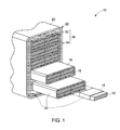
- FIG. 1 is a schematic representation of an electrical system 10.
- the system 10 includes an electrically conducting material 12 for passing electrical current between medium or high voltage points. Copper, aluminum, silver, gold, or any other good conductor of electricity may be used as a conducting material 12.
- the electrically conducting material 12 may be in the form of a strand having an outer insulation cover, such as strand insulation 14, on each strand of the electrically conducting material 12.
- the strand insulation 14 includes varnish, enamel compounds, or glass.
- the strand insulation 14 for each individual conductor 12 includes a corona resistant nano composite enamel or extruded coating.
- the conductor 12 may be fused with a polymeric film that is filled with nanoparticles of mineral or metal oxides.
- the particle size of the nanoparticles in the film may vary, depending on the nanoparticle compositions.
- the average size of the nanoparticle in the polymeric film varies in a range from about 1 nm to about 100 nm.
- the average size of a nanoparticle is the distribution of the particles as observed in particle imaging techniques, and measured along the smallest dimension of the particle. For example, if the particles are of circular shape, the smallest dimension is the diameter of the sphere, while if the particles are "plate” shaped, the greatest dimension is the length of the plate; and the smallest dimension is the thickness of the plate.
- "average” is the calculated mean of the particle sizes observed during imaging, or the median value of the particle distribution curve.
- the average size of the nanoparticle in the dielectric fluid varies in a range from about 5 nm to about 50 nm.
- the insulated strands may be grouped together and wound in the form of turns 16 in the machine, having a turn to turn insulation 18, referred hereinafter as turn insulation 18.
- the turn insulation 18 separates a group of insulated conductor strands.
- the conductor strands 12 with a turn insulation 18 may be referred to as turn insulated conductor strands.
- the turn insulation 18 may also be referred to as a phase-to-phase insulation between adjacent coils in different phase groups. A failure of turn insulation 18 could lead to turn-to-turn electrical shorts.
- the turn insulated conductor strands would typically be wrapped with another insulation that would provide insulation from the electrical ground.
- the wrapped form may be housed inside a casing 20.
- the insulation between the numerous turns and the casing 20 is termed as "ground wall insulation” 22.
- An electrical insulation system 24 of the system 10 usually includes at least three sections or portions: the strand insulation 14, turn insulation 18, and the ground wall insulation 22.
- turn-to-turn shorts are one of the more prevalent and potentially destructive electrical faults in inverter-driven AC machines such as induction motors, for example.
- inverter-driven AC machines such as induction motors, for example.
- these localized faults produce thermal hot spots that foster progressive degradation, and may mature into turn-to-ground faults, thereby breaking the ground wall insulation 22.
- the turn insulation is formed as an insulating tape or wrapper surrounding the group of individual conductors which have been formed into a predetermined shape to form a coil.
- the turn insulation is further made of a layer of mica tape. Flakes of mica provide an insulation resistance to corona discharge, which tends to increase as operating voltage levels of the rotating machines increase.
- Addition of particles of alumina or silica to polymeric compositions of strand or turn insulation may be advantageously used to enhance the corona resistance of the insulation, and may further improve the heat transfer characteristics of the conductor insulation.
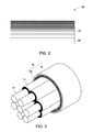
- the electrical insulation system 24 includes a layered insulation tape 30 ( FIG. 1 , 2, 3 ) having at least two layers.
- a first layer 32 of the tape 30 may include mica paper and a binder resin.
- a second layer 34 comprises a composite of layered nanoparticles dispersed in a polyetheretherketone (PEEK) matrix.
- PEEK polyetheretherketone
- Mica generally has a crystalline structure and forms layers that can be split or delaminated into thin sheets as mica paper. These sheets are chemically inert, dielectric, elastic, flexible, hydrophilic, insulating, lightweight, reflective, refractive, resilient, and range in opacity from transparent to opaque. Mica is stable when exposed to electricity, light, moisture, and extreme temperatures. It has superior electrical properties as an insulator and as a dielectric, has a high dielectric breakdown, is thermally stable up to about 500°C, and is resistant to corona discharge. Specifically, mica is unusual, in that it is a good electrical insulator while also being a good thermal conductor.
- the binder resin may bind the mica papers together to be used in the form of a mica tape as the first layer.
- the amount of the binder resin in the mica tape is in a range from about 2 wt% to about 10 wt%. In an alternate embodiment, the amount of the binder resin in the mica tape is in a range from about 3 wt% to about 6 wt%.
- the binder resin present in the mica tape may include nanofillers.
- the nanofillers may include alumina, silica, titania, boron nitride, aluminum nitride, aluminum silicates, nanoclay, or talc.
- first layer 32 ( FIG. 2 ) of mica tape may be enhanced by supporting the first layer with a polymer film.
- Polymer films have excellent flexibility and breakdown strength, and hence the mica tape may be laminated with the film to provide good mechanical strength for wire wrapping processes.
- the generally used polymer films may degrade in the presence of a partial discharge or corona. The films may erode and become a weak link in the insulation system 24.
- a second layer 34 comprising a PEEK film is used as a backing for the first layer 32 having the mica tape.
- PEEK is a semicrystalline thermoplastic polymer having a glass transition temperature of about 143°C, and a melting point around 343°C. PEEK has excellent mechanical and chemical resistance properties that are retained well above room temperature. PEEK is highly resistant to thermal degradation, and further has good thermal conductivity that increases with temperature. Using PEEK as a support for mica tape would increase the thermal and corona stability of the insulation system 24.
- the nanocrystallines that are present in the PEEK film have a layered structure.
- the layered structure of a nanocrystalline material may be assessed through the basal cleavage ability of its crystal structure.
- a material that has a perfect or near-perfect basal cleavage in any one crystal plane is generally considered as having a layered structure.
- the layered nanoparticles have an aspect ratio in a range from about 10 to about 100.
- the aspect ratio is defined as the ratio of length (longest dimension) to the thickness (shortest dimension) of a single layer. In one embodiment, the aspect ratio is in a range from about 20 to about 100.
- Nanoclay and talc are two examples of layered materials that may be readily embedded in the PEEK film when the PEEK film is used as a carrier for the mica layer.
- nanoclays are nanoparticles of layered mineral silicates.
- the strand insulation 14 is fused with the PEEK film that is filled with layered nanoparticles of mineral or metal oxides.
- Clay may be a combination of one or more clay minerals, mostly composed of phyllosilicate minerals.
- the most abundantly available clay in nature may include kaolinite, montmorillonite-smectite, illite, and chlorite.
- Clay minerals are normally built of tetrahedral silicate sheets and octahedral hydroxide sheets, with either a 1:1 ratio of tetrahedral to octahedral sheets, or with 2:1 ratio of tetrahedral to octahedral sheets.
- Another of the nanoparticles described above, talc is a mineral that is generally composed of hydrated magnesium silicate, and has a monoclinic or triclinic crystal system. Talc is said to have a perfect basal cleavage on a ⁇ 001 ⁇ plane.
- the composite of PEEK film and the layered nanoparticles may include nanoparticles in a range from about 10 wt% to about 40 wt% of the second layer 34.
- the percentage of the layered nanoparticles in the second layer 34 of PEEK composite is in a range from about 10 wt% to about 40 wt%, based on the total weight of the PEEK and layered nanoparticles.
- the composite may include layered nanoparticles in a range from about 20 wt% to about 30 wt% of the second layer 34.
- the first layer 32 of the insulation tape 30, having the mica tape may be positioned to be proximate to the electrical conductor material 12.
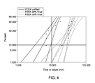
- the first layer 32 is in contact with the electrically conducting material 12, as shown in FIG. 3 .
- "in contact with the electrically conducting material 12" would include a physical contact with the insulated electrically conducting material 12, but does not necessarily mean that the layer 32 is in electrical communication with the electrically conducting material 12.
- the second layer 34 having the PEEK composite may be adjacent to the first layer 32, laminating the first layer 32.
- the first layer 32 and the second layer 34 may be laminated with or without using a binder resin.
- the binder resin present in the first layer 32 is sufficient to join the second layer 34 with the first layer 32.
- the first layer 32 is directly joined to the second layer 34 to form the layered insulation tape 30.
- directly joined implies that the first layer 32 is attached to the second layer 34 without specifically using any binder or any other material in-between the two layers.
- a small amount of a binder resin may be used in-between the first layer 32 and the second layer 34 for laminating.
- the binder resin that is used for laminating the first layer 32 with the second layer 34 may or may not be same as the binder resin that is used in the mica tape.
- the amount of the binder resin in the insulation tape 30 is in a range from about 3 wt% to about 10 wt%. In a specific embodiment, the amount of the binder resin in the insulation tape 30 is in a range from about 5 wt% to about 12 wt%, and in some preferred embodiments, the amount is in the range from about 8 wt% to about 10 wt%.
- the first layer 32 is sandwiched between the strand insulated conductor 12 and the second layer 34.
- the second layer 34 enfolds the first layer 32.
- the enfolding of the first layer 32 by the second layer 34 means that the second layer 34 substantially covers one surface of the first layer 32.
- one surface of the first layer 32 may be open to the strand insulated conductor and the other, opposite surface may be completely covered by the second layer 34.
- the depiction of the layers in FIG. 3 is used for illustration, and may be interchanged, depending on the applications.
- the layer 34 having a PEEK composite, may be adjacent to the electrically conducting material 12 or the strand insulated conductor, and layer 32, including mica tape, may enfold the layer 34.
- the first layer 32 and the second layer 34 may include many sub-layers within, and in one embodiment, there are several alternate layers of first 32 and second 34 layers in an insulation tape 30 ( FIGS. 1 , 2 and 3 ).
- the layered insulation tape 30 may be used as turn insulation 18, ground wall insulation 22, or both.
- the insulation system having the strand insulation 14, turn insulation 18 ( FIGS. 1 , 3 ), and ground wall insulation 22 ( FIG. 1 ), is further impregnated by a resin having nanofillers (nanofiller-incorporated resin), using a vacuum pressure impregnation method.
- Vacuum pressure impregnation processes are known in the art, and described, for example, in the book Industrial Power Engineering Handbook By KC Agrawal, published by Newnes on 08th Oct-2001, pages 9/222-9/224 .
- the vacuum pressure impregnation method is used to impregnate the whole system 10, so that the nanofiller-incorporated resin is impregnated throughout the system.
- This method of impregnating the entire system is sometimes termed a "global vacuum impregnation" method.
- the nanofiller-incorporated resin impregnation becomes a part of the insulation system 24 within the system 10 ( FIG. 1 ), further aiding the reduction of air gaps in the system 10.
- the resin used in the global vacuum pressure impregnation of the system 10 may be the same or different from the binder resin used along with the mica paper in the first layer 32 ( FIGS. 2 and 3 ).
- the nanofillers used in the vacuum pressure impregnation step may include alumina, silica, titania, boron nitride, aluminum nitride, aluminum silicates, nanoclay, and talc. Adding a small amount of nanofillers to the binder resin may alter the resin viscosity.
- nanofillers may be functionalized. "Functionalization” refers to a method of increasing the reactivity of the nanofiller surface. Functionalization may be accomplished by a surface coating or treatment with a functionalizing agent, which reacts with sites on the surface of the nanofillers, increasing the activity of those sites.
- the nanofillers were treated with silane functional groups to facilitate the compatibility of the nanofillers with the host resin, so as to maintain resin viscosity as low as pure resin.
- the average particle size of the nanofillers may be less than about 100 nanometers, and further, may be less than about 50 nanometers.
- the average size of a nanofiller is the distribution of the particles as observed in particle imaging techniques, and measured along its smallest dimension. Further, "average” is the calculated mean of the particle sizes observed during imaging.
- the nanofillers may be finely dispersed in the binder resin. In one embodiment, some of the nanofillers may be agglomerated. The average size of the agglomeration of nanofillers may be less than about 1 micrometer.
- nanofillers-filled resin for brevity
- the nanofillers-filled resin impregnated in the insulation system by the global vacuum pressure impregnation method may fill-in most of or all of the gaps in the insulation system 24 itself, and may also fill any gaps between the conductor 12 and the insulation system 24. Therefore, the nano-filled resin may be impregnated between the conductor 12 and the strand insulation 14; between the strand insulation 14 and the turn insulation 18; and between the turn insulation 18 and the ground wall insulation 22.
- One example of the possible gap in the electrical system 10 is between the strand insulated conductor 12 coils (alternately "coil gaps").
- the amount of the nanofillers in the global vacuum impregnated resin may be in a range from about 0.1 wt% to about 5 wt%, and in some specific embodiments, in the range from about 0.5 wt% to about 3 wt%, based on the total weights of resin and nanofillers.
- This amount of nanofillers is very low, as compared to levels normally used in vacuum-impregnated resins.
- the nanofillers were added to increase the thermal conductivity of the overall insulation system by using the enhanced thermal conductivity of the nanofillers as compared to the resin material. Therefore, it was surprising to learn that relatively low amounts of nanofillers could be effective in this insulation system, since prior experience appeared to show a requirement for increasing amounts of nanofillers in order to achieve increasing levels of thermal conductivity".
- the mechanism of increasing the insulation by using a small amount (less than 5 wt%) of nanofillers in the global vacuum impregnated resin discussed herein is different from the mechanism for the above-mentioned, earlier used nanofiller addition.
- the low amount of nanofillers in the resin used herein assists in resin retention in the coil gap, by lowering the viscosity drop as compared to the pure resin, during heat ramping to curing or baking temperature. Because of the low viscosity drop, the undesirable run-off of resin during the curing process is minimized. With enhanced resin filling in coil gaps, the air pockets are reduced, and the effective thermal conductivity of the insulation is increased. This can lead to better heat transfer.
- the nano-filled resin increases corona resistance, and prolongs voltage endurance, aiding in the enhancement of the service life of the system 10.
- a PEEK film (AptivTM 1000), mineral filled PEEK film (AptivTM 1102, AptivTM 1103), and a pure epoxy (class H resin, EpoxyliteTM, Von RollTM 3407) with nanofillers (Al 2 O 3 , TiO 2 , SiO 2 ), were used as samples for testing.
- Epoxy curing characteristics such as curing onset temperature, heat of reaction, viscosity, and thermal stability, were studied.
- Mineral filled PEEK film was characterized by viewing the filler structure images by SEM, and determining the chemical composition of fillers.
- the chemical resistance of the PEEK film vs. mineral filled PEEK film was compared by measuring in a 1% H 2 S, 1% CO 2 , 1% CH 4 and 97% N 2 , 5% H 2 O atmosphere.
- the pulse endurance test was conducted at 1.2 kV, 20 kHz switching frequency, with a duty cycle of 50% and dV/dt of 20kV/ ⁇ s. All of the test results were collected at STP with relative humidity (RH) ranging from 30% to 50%.
- the upper electrode was a 1 ⁇ 4 inch diameter ball electrode.
- the bottom electrode was a 4 inch diameter flat disk.
- the mineral filled PEEK films exhibited equally good chemical resistance as compared to the unfilled PEEK film, when tested at the corrosive gas environment at a temperature of about 150°C, and a pressure of about 150 bars.
- the AC dielectric strength of both mineral filled and unfilled PEEK films did not show appreciable change after corrosive environment aging, as seen from FIGS. 6A and 6B . Therefore, when the talc filled PEEK film is used as turn insulation and ground wall insulation in conjunction with mica paper, machine performance enhancement in both the corona resistance and heat transfer improvement is expected.
- nanofillers does not affect the heat of reaction, Tg, or thermal stability, but has a positive effect on the viscosity, as seen from FIG. 7 .
- This positive effect on the viscosity is expected to result in reduced resin run-out, decreased air pockets, and better heat transfer. This property further aids in the overall electrical insulation of the insulation system 24.
Landscapes
- Engineering & Computer Science (AREA)
- Power Engineering (AREA)
- Manufacturing & Machinery (AREA)
- Physics & Mathematics (AREA)
- Spectroscopy & Molecular Physics (AREA)
- Chemical & Material Sciences (AREA)
- Inorganic Chemistry (AREA)
- Insulating Bodies (AREA)
- Insulation, Fastening Of Motor, Generator Windings (AREA)
- Inorganic Insulating Materials (AREA)
- Organic Insulating Materials (AREA)
Abstract
Description
- The invention relates generally to electrical insulation systems. More particularly, some embodiments of the invention relate to electrical insulation systems including multi-strand, multi-turn conductor winding insulation and ground wall insulation, in a medium or high voltage rotating machine.
- With the use of any electrical machines, there is a need to electrically insulate the conductors in the machines. The need for electrical insulation in the machines increases with higher operating voltages. With increasing use of pulse width modulated (PWM) drives, electric machines experience premature electrical failure caused by higher electrical stress on winding insulation, due in part to uneven voltage distribution under high dV/dt conditions. One way to address insulation deficiency is to increase insulation build. However, this can lead to large machine size and poor heat conduction. Thus, a better insulation system that can enable reduction of electrical machine size for high power applications is desired.
- Another need within an electrical machine is thermal energy dissipation. Therefore, there is a need for thermally conductive electrical insulators in medium or high voltage electrical machines. Further, insulation systems with higher mechanical strength and thermal stability are sometimes very desirable.
- Traditionally, various epoxy resins, mica tapes, or glass fibers were used in electrical insulation systems. However, microvoids may be created during the impregnation or curing of the epoxy resins, leading to poor thermal conduction and partial discharge. Further, the partial discharge resistance of epoxy resins or pure polymer films may be lower than required for certain electrical machines. Mica tapes and glass fibers may not have the mechanical stability required for the robust performance of the electrical machine.
- Mica tape made of mica paper with polyester film demonstrated good taping quality and high breakdown strength. However it can be deficient, in terms of long term voltage endurance, due to the poor corona resistance of polyester film. Mica tape made of mica paper with fiberglass is known to have good long term voltage endurance performance, but can have poor taping quality and lower dielectric breakdown strength. The thermal conductivity of mica tape may be increased by adding thermally conductive particulates to the binding resin. This is particularly suitable for resin-rich mica tape, for heat press or autoclave processes, but may not be good for mica tape that is used in vacuum pressure impregnated (VPI) machines, for high power applications.
- Therefore, there is a need for a comprehensive approach to the electrical insulation system of medium to high voltage electrical machines, e.g., those that operate in the range of about 4160 V to 15000 V.
- In one embodiment, a system is presented. The system includes an electrically conducting material and an electrical insulation system. The electrical insulation system includes a layered insulation tape that has a first layer and a second layer. The first layer includes mica paper and a binder resin in a range from about 5 wt% to about 12 wt% of the insulated tape. The second layer includes a composite of layered nanoparticles dispersed in a polyetheretherketone (PEEK) matrix. The second layer laminates the first layer.
- In another embodiment, a system is also presented. The system includes strands of an electrically conducting material and an electrical insulation system. The electrical insulation system includes a strand insulation, a turn insulation, and a ground wall insulation. The strand insulation includes a composite of layered nanoparticles in a PEEK matrix and insulates the strands of the electrically conducting material. The turn insulation and ground wall insulation include a layered insulation tape. The layered insulation tape includes a first layer and a second layer. The first layer includes a mica paper and a binder resin from about 5 wt% to about 12 wt% of layered insulation tape. The second layer includes a composite of layered nanoparticles dispersed in a polyetheretherketone (PEEK) matrix. The second layer laminates the first layer in the insulation tape. The insulation system further includes a vacuum impregnated resin that includes nanofillers in a range from about 0.1 wt% to about 5 wt%.
- Yet another embodiment includes a method of forming an insulation system. The method includes incorporating mica paper and a binder resin to form a first layer; incorporating layered nanoparticles in a PEEK matrix to form a second layer; forming a layered insulation tape by attaching the first layer and the second layer; shaping the layered insulation tape as a turn insulation and ground wall insulation for an electrically conducting material in a system; and impregnating the system with nanofiller-incorporated resin, using a vacuum pressure impregnation method to form an insulation system within the system.
- These and other features, aspects, and advantages of the present invention will become better understood when the following detailed description is read with reference to the accompanying drawings, in which like characters represent like parts throughout the drawings, wherein:
-
FIG. 1 is a schematic diagram of a multi-strand, multi-turn conductor, according to one embodiment of the invention; -
FIG. 2 is a schematic cross-sectional representation of a layered insulation tape, according to one embodiment of the invention; -
FIG. 3 is a schematic cross-sectional representation of a turn insulation insulating a strand insulated conducting material, according to one embodiment of the invention; -
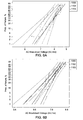
FIG. 4 is a comparative graph of the pulse endurance of PEEK film and talc-filled PEEK film; -
FIG. 5 is a comparative graph of the tensile modulus of a PEEK film and a talc filled PEEK film; -
FIG. 6A is a graph of AC Breakdown voltage of a virgin PEEK film andFIG. 6B is a graph of AC Breakdown voltage of an aged PEEK film; and -
FIG. 7 is comparative graph of the viscosity of epoxy resin and PEEK film that is filled with layered nanoparticles. - Embodiments of the present invention describe a system including electrically conducting materials; and electrical insulation systems surrounding the electrically conducting materials.
- One or more specific embodiments of the present invention are described below. In an effort to provide a concise description of these embodiments, all features of an actual implementation may not be described in the specification. It should be appreciated that in the development of any such actual implementation, as in any engineering or design project, numerous implementation-specific decisions must be made to achieve the developers' specific goals, such as compliance with system-related and business-related constraints, which may vary from one implementation to another. Moreover, it should be appreciated that such a development effort might be complex and time consuming, but would nevertheless be a routine undertaking of design, fabrication, and manufacture for those of ordinary skill having the benefit of this disclosure.
- In the following specification and the claims that follow, the singular forms "a", "an" and "the" include plural referents unless the context clearly dictates otherwise.
- Approximating language, as used herein throughout the specification and claims, may be applied to modify any quantitative representation that could permissibly vary, without resulting in a change in the basic function to which it is related. Accordingly, a value modified by a term such as "about" is not to be limited to the precise value specified. In some instances, the approximating language may correspond to the precision of an instrument for measuring the value.
- A medium voltage (4 kV to 15 kV) inverter may be used in different applications such as fans, compressors, pumps, mixers, extruders, wind turbines, wind and water tunnels, mine winders, conveyors, test benches, high speed drives for oil and gas, drives for marine, naval, and metals industry, for example. The medium voltage inverters need to be compact, and have high efficiency performance and reliability. A wide-ranging, reliable insulation system would aid in extending the use of medium voltage electrical machines.
FIG. 1 is a schematic representation of anelectrical system 10. Thesystem 10 includes an electrically conductingmaterial 12 for passing electrical current between medium or high voltage points. Copper, aluminum, silver, gold, or any other good conductor of electricity may be used as a conductingmaterial 12. Theelectrically conducting material 12 may be in the form of a strand having an outer insulation cover, such asstrand insulation 14, on each strand of theelectrically conducting material 12. Traditionally thestrand insulation 14 includes varnish, enamel compounds, or glass. In one embodiment of the invention, thestrand insulation 14 for eachindividual conductor 12 includes a corona resistant nano composite enamel or extruded coating. Theconductor 12 may be fused with a polymeric film that is filled with nanoparticles of mineral or metal oxides. - The particle size of the nanoparticles in the film may vary, depending on the nanoparticle compositions. In one embodiment, the average size of the nanoparticle in the polymeric film varies in a range from about 1 nm to about 100 nm. As used herein, the average size of a nanoparticle is the distribution of the particles as observed in particle imaging techniques, and measured along the smallest dimension of the particle. For example, if the particles are of circular shape, the smallest dimension is the diameter of the sphere, while if the particles are "plate" shaped, the greatest dimension is the length of the plate; and the smallest dimension is the thickness of the plate. Further, "average" is the calculated mean of the particle sizes observed during imaging, or the median value of the particle distribution curve. In a further embodiment, the average size of the nanoparticle in the dielectric fluid varies in a range from about 5 nm to about 50 nm.
- The insulated strands may be grouped together and wound in the form of
turns 16 in the machine, having a turn to turninsulation 18, referred hereinafter asturn insulation 18. Thus, theturn insulation 18 separates a group of insulated conductor strands. Theconductor strands 12 with aturn insulation 18 may be referred to as turn insulated conductor strands. Theturn insulation 18 may also be referred to as a phase-to-phase insulation between adjacent coils in different phase groups. A failure ofturn insulation 18 could lead to turn-to-turn electrical shorts. - The turn insulated conductor strands would typically be wrapped with another insulation that would provide insulation from the electrical ground. The wrapped form may be housed inside a
casing 20. The insulation between the numerous turns and thecasing 20 is termed as "ground wall insulation" 22. Anelectrical insulation system 24 of thesystem 10 usually includes at least three sections or portions: thestrand insulation 14,turn insulation 18, and theground wall insulation 22. - The turn-to-turn shorts are one of the more prevalent and potentially destructive electrical faults in inverter-driven AC machines such as induction motors, for example. Arising primarily from insulation degradation (through contamination or abnormal thermal, mechanical, electrical or other environmental stresses), these localized faults produce thermal hot spots that foster progressive degradation, and may mature into turn-to-ground faults, thereby breaking the
ground wall insulation 22. - As the voltage ratings of machines tend to reach higher levels, improved ways to increase the gradients for electrical potentials need to be developed without increasing the thickness of the insulation. In rotating machines especially, the turn insulation is formed as an insulating tape or wrapper surrounding the group of individual conductors which have been formed into a predetermined shape to form a coil. The turn insulation is further made of a layer of mica tape. Flakes of mica provide an insulation resistance to corona discharge, which tends to increase as operating voltage levels of the rotating machines increase.
- Addition of particles of alumina or silica to polymeric compositions of strand or turn insulation may be advantageously used to enhance the corona resistance of the insulation, and may further improve the heat transfer characteristics of the conductor insulation.
- In one embodiment, the
electrical insulation system 24 includes a layered insulation tape 30 (FIG. 1 ,2, 3 ) having at least two layers. Afirst layer 32 of thetape 30 may include mica paper and a binder resin. Asecond layer 34 comprises a composite of layered nanoparticles dispersed in a polyetheretherketone (PEEK) matrix. - Mica generally has a crystalline structure and forms layers that can be split or delaminated into thin sheets as mica paper. These sheets are chemically inert, dielectric, elastic, flexible, hydrophilic, insulating, lightweight, reflective, refractive, resilient, and range in opacity from transparent to opaque. Mica is stable when exposed to electricity, light, moisture, and extreme temperatures. It has superior electrical properties as an insulator and as a dielectric, has a high dielectric breakdown, is thermally stable up to about 500°C, and is resistant to corona discharge. Specifically, mica is unusual, in that it is a good electrical insulator while also being a good thermal conductor.
- The binder resin may bind the mica papers together to be used in the form of a mica tape as the first layer. In one embodiment, the amount of the binder resin in the mica tape is in a range from about 2 wt% to about 10 wt%. In an alternate embodiment, the amount of the binder resin in the mica tape is in a range from about 3 wt% to about 6 wt%.
- In one embodiment, the binder resin present in the mica tape may include nanofillers. The nanofillers may include alumina, silica, titania, boron nitride, aluminum nitride, aluminum silicates, nanoclay, or talc.
- Mechanical properties of mica allow it to be cut, punched, stamped, and machined to close tolerances. Mica needs a strong mechanical carrier (alternately, "backing layer") that provides good mechanical strength for its application in medium and high voltage machines. Therefore, the mechanical durability of the first layer 32 (
FIG. 2 ) of mica tape may be enhanced by supporting the first layer with a polymer film. Polymer films have excellent flexibility and breakdown strength, and hence the mica tape may be laminated with the film to provide good mechanical strength for wire wrapping processes. However, the generally used polymer films may degrade in the presence of a partial discharge or corona. The films may erode and become a weak link in theinsulation system 24. Hence, in one embodiment of the present invention, asecond layer 34 comprising a PEEK film is used as a backing for thefirst layer 32 having the mica tape. - PEEK is a semicrystalline thermoplastic polymer having a glass transition temperature of about 143°C, and a melting point around 343°C. PEEK has excellent mechanical and chemical resistance properties that are retained well above room temperature. PEEK is highly resistant to thermal degradation, and further has good thermal conductivity that increases with temperature. Using PEEK as a support for mica tape would increase the thermal and corona stability of the
insulation system 24. - Further, it was envisaged by the inventors that using nanocrystalline mineral filled PEEK composite instead of pure PEEK film as the support (carrier) would enhance the heat transfer and voltage endurance of the insulation tape. In one embodiment, the nanocrystallines that are present in the PEEK film have a layered structure. As used herein, the layered structure of a nanocrystalline material may be assessed through the basal cleavage ability of its crystal structure. A material that has a perfect or near-perfect basal cleavage in any one crystal plane is generally considered as having a layered structure. In one embodiment, the layered nanoparticles have an aspect ratio in a range from about 10 to about 100. As used herein, the aspect ratio is defined as the ratio of length (longest dimension) to the thickness (shortest dimension) of a single layer. In one embodiment, the aspect ratio is in a range from about 20 to about 100.
- Nanoclay and talc are two examples of layered materials that may be readily embedded in the PEEK film when the PEEK film is used as a carrier for the mica layer. As used herein, nanoclays are nanoparticles of layered mineral silicates. In one embodiment, along with using the PEEK film for the
insulation tape 30, thestrand insulation 14 is fused with the PEEK film that is filled with layered nanoparticles of mineral or metal oxides. - Clay may be a combination of one or more clay minerals, mostly composed of phyllosilicate minerals. The most abundantly available clay in nature may include kaolinite, montmorillonite-smectite, illite, and chlorite. Clay minerals are normally built of tetrahedral silicate sheets and octahedral hydroxide sheets, with either a 1:1 ratio of tetrahedral to octahedral sheets, or with 2:1 ratio of tetrahedral to octahedral sheets. Another of the nanoparticles described above, talc, is a mineral that is generally composed of hydrated magnesium silicate, and has a monoclinic or triclinic crystal system. Talc is said to have a perfect basal cleavage on a {001} plane.
- The composite of PEEK film and the layered nanoparticles may include nanoparticles in a range from about 10 wt% to about 40 wt% of the
second layer 34. The percentage of the layered nanoparticles in thesecond layer 34 of PEEK composite is in a range from about 10 wt% to about 40 wt%, based on the total weight of the PEEK and layered nanoparticles. In one embodiment, the composite may include layered nanoparticles in a range from about 20 wt% to about 30 wt% of thesecond layer 34. - The
first layer 32 of theinsulation tape 30, having the mica tape, may be positioned to be proximate to theelectrical conductor material 12. In one embodiment, thefirst layer 32 is in contact with theelectrically conducting material 12, as shown inFIG. 3 . As used herein, "in contact with theelectrically conducting material 12" would include a physical contact with the insulated electrically conductingmaterial 12, but does not necessarily mean that thelayer 32 is in electrical communication with theelectrically conducting material 12. For example, there could be an intervening, electrical-insulation layer present, such as thestrand insulation 14, and hence thefirst layer 32 of theinsulation tape 30, having the mica tape, may be positioned to be proximate to the strand insulated electrical conductor material. - The
second layer 34 having the PEEK composite may be adjacent to thefirst layer 32, laminating thefirst layer 32. Thefirst layer 32 and thesecond layer 34 may be laminated with or without using a binder resin. In an embodiment, the binder resin present in thefirst layer 32 is sufficient to join thesecond layer 34 with thefirst layer 32. In one embodiment, thefirst layer 32 is directly joined to thesecond layer 34 to form the layeredinsulation tape 30. As used herein, "directly joined" implies that thefirst layer 32 is attached to thesecond layer 34 without specifically using any binder or any other material in-between the two layers. - In an alternate embodiment, a small amount of a binder resin may be used in-between the
first layer 32 and thesecond layer 34 for laminating. The binder resin that is used for laminating thefirst layer 32 with thesecond layer 34 may or may not be same as the binder resin that is used in the mica tape. In one embodiment, the amount of the binder resin in theinsulation tape 30 is in a range from about 3 wt% to about 10 wt%. In a specific embodiment, the amount of the binder resin in theinsulation tape 30 is in a range from about 5 wt% to about 12 wt%, and in some preferred embodiments, the amount is in the range from about 8 wt% to about 10 wt%. - In one embodiment, the
first layer 32 is sandwiched between the strand insulatedconductor 12 and thesecond layer 34. In an exemplary embodiment, thesecond layer 34 enfolds thefirst layer 32. As used herein, the enfolding of thefirst layer 32 by thesecond layer 34 means that thesecond layer 34 substantially covers one surface of thefirst layer 32. In the sandwich arrangement, one surface of thefirst layer 32 may be open to the strand insulated conductor and the other, opposite surface may be completely covered by thesecond layer 34. - As used herein, the depiction of the layers in
FIG. 3 is used for illustration, and may be interchanged, depending on the applications. For example, thelayer 34, having a PEEK composite, may be adjacent to theelectrically conducting material 12 or the strand insulated conductor, andlayer 32, including mica tape, may enfold thelayer 34. Further thefirst layer 32 and thesecond layer 34 may include many sub-layers within, and in one embodiment, there are several alternate layers of first 32 and second 34 layers in an insulation tape 30 (FIGS. 1 ,2 and 3 ). Thelayered insulation tape 30 may be used asturn insulation 18,ground wall insulation 22, or both. - In one embodiment, the insulation system having the
strand insulation 14, turn insulation 18 (FIGS. 1 ,3 ), and ground wall insulation 22 (FIG. 1 ), is further impregnated by a resin having nanofillers (nanofiller-incorporated resin), using a vacuum pressure impregnation method. Vacuum pressure impregnation processes are known in the art, and described, for example, in the book Industrial Power Engineering Handbook By KC Agrawal, published by Newnes on 08th Oct-2001, . In one embodiment, the vacuum pressure impregnation method is used to impregnate thewhole system 10, so that the nanofiller-incorporated resin is impregnated throughout the system. This method of impregnating the entire system is sometimes termed a "global vacuum impregnation" method. The nanofiller-incorporated resin impregnation becomes a part of theinsulation system 24 within the system 10 (FIG. 1 ), further aiding the reduction of air gaps in thesystem 10. The resin used in the global vacuum pressure impregnation of thesystem 10 may be the same or different from the binder resin used along with the mica paper in the first layer 32 (FIGS. 2 and 3 ). - The nanofillers used in the vacuum pressure impregnation step may include alumina, silica, titania, boron nitride, aluminum nitride, aluminum silicates, nanoclay, and talc. Adding a small amount of nanofillers to the binder resin may alter the resin viscosity.
- The surface of these nano fillers may be functionalized. "Functionalization" refers to a method of increasing the reactivity of the nanofiller surface. Functionalization may be accomplished by a surface coating or treatment with a functionalizing agent, which reacts with sites on the surface of the nanofillers, increasing the activity of those sites. In one embodiment, the nanofillers were treated with silane functional groups to facilitate the compatibility of the nanofillers with the host resin, so as to maintain resin viscosity as low as pure resin.
- The average particle size of the nanofillers may be less than about 100 nanometers, and further, may be less than about 50 nanometers. As used herein, the average size of a nanofiller is the distribution of the particles as observed in particle imaging techniques, and measured along its smallest dimension. Further, "average" is the calculated mean of the particle sizes observed during imaging. The nanofillers may be finely dispersed in the binder resin. In one embodiment, some of the nanofillers may be agglomerated. The average size of the agglomeration of nanofillers may be less than about 1 micrometer.
- The nanofillers-filled resin ("nano-filled resin" for brevity) impregnated in the insulation system by the global vacuum pressure impregnation method may fill-in most of or all of the gaps in the
insulation system 24 itself, and may also fill any gaps between theconductor 12 and theinsulation system 24. Therefore, the nano-filled resin may be impregnated between theconductor 12 and thestrand insulation 14; between thestrand insulation 14 and theturn insulation 18; and between theturn insulation 18 and theground wall insulation 22. One example of the possible gap in theelectrical system 10 is between the strand insulatedconductor 12 coils (alternately "coil gaps"). - The amount of the nanofillers in the global vacuum impregnated resin may be in a range from about 0.1 wt% to about 5 wt%, and in some specific embodiments, in the range from about 0.5 wt% to about 3 wt%, based on the total weights of resin and nanofillers. This amount of nanofillers is very low, as compared to levels normally used in vacuum-impregnated resins. In the past, the nanofillers were added to increase the thermal conductivity of the overall insulation system by using the enhanced thermal conductivity of the nanofillers as compared to the resin material. Therefore, it was surprising to learn that relatively low amounts of nanofillers could be effective in this insulation system, since prior experience appeared to show a requirement for increasing amounts of nanofillers in order to achieve increasing levels of thermal conductivity".
- The mechanism of increasing the insulation by using a small amount (less than 5 wt%) of nanofillers in the global vacuum impregnated resin discussed herein is different from the mechanism for the above-mentioned, earlier used nanofiller addition. The low amount of nanofillers in the resin used herein assists in resin retention in the coil gap, by lowering the viscosity drop as compared to the pure resin, during heat ramping to curing or baking temperature. Because of the low viscosity drop, the undesirable run-off of resin during the curing process is minimized. With enhanced resin filling in coil gaps, the air pockets are reduced, and the effective thermal conductivity of the insulation is increased. This can lead to better heat transfer. In addition, the nano-filled resin increases corona resistance, and prolongs voltage endurance, aiding in the enhancement of the service life of the
system 10. - The following examples illustrate methods, materials and results, in accordance with specific embodiments, and as such should not be construed as imposing limitations upon the claims. All components are commercially available from common chemical suppliers.
- The processability, manufacturability, dielectric capability, viability, and moisture and H2S/CO2 resistance of an exemplary insulation tape and nano-filled, global vacuum impregnated resin was tested for the application of a medium voltage rotating machine insulation.
- A PEEK film (Aptiv™ 1000), mineral filled PEEK film (
Aptiv™ 1102, Aptiv™ 1103), and a pure epoxy (class H resin, Epoxylite™, Von Roll™ 3407) with nanofillers (Al2O3, TiO2, SiO2), were used as samples for testing. The AC breakdown strength, dissipation factor, and pulse endurance of the pure epoxy vs. nano-filled epoxy; and PEEK film vs. mineral filled PEEK film, were compared. Epoxy curing characteristics, such as curing onset temperature, heat of reaction, viscosity, and thermal stability, were studied. Mineral filled PEEK film was characterized by viewing the filler structure images by SEM, and determining the chemical composition of fillers. The chemical resistance of the PEEK film vs. mineral filled PEEK film was compared by measuring in a 1% H2S, 1% CO2, 1% CH4 and 97% N2, 5% H2O atmosphere. - When the glass transition temperature (Tg), frequency response of dielectric constant and loss tangent, and dielectric strength of the PEEK film were compared with that of mineral filled PEEK films, there was not much observable change because of the addition of layered nanoparticles. However, there was about a "3X" improvement in the pulse endurance for the talc filled PEEK films that had a thickness of about 25 µm as compared to the PEEK film (same thickness) without any nanoparticles, as shown in
FIG. 4 . No significant difference was observed between 20% and 30% filler concentrations of talc filled PEEK films of the above mentioned thickness. The pulse endurance test was conducted at 1.2 kV, 20 kHz switching frequency, with a duty cycle of 50% and dV/dt of 20kV/µs. All of the test results were collected at STP with relative humidity (RH) ranging from 30% to 50%. The upper electrode was a ¼ inch diameter ball electrode. The bottom electrode was a 4 inch diameter flat disk. - Further, a comparison was made for the samples of talc-filled PEEK film of about 50µm thickness, as compared to that of unfilled films of the same thickness. An approximate 10X improvement in pulse endurance at 1.6 kV pulse voltage was observed, as shown in Table 1, along with at least 30% higher thermal conductivity, as shown in Table 2, and about a 100% increase in the tensile modulus, as shown in
FIG. 5 . Mineral fillers present in the film are layered structure flakes. Therefore, thermal conductivity of the mineral filled PEEK films (APTIV1102 and APTIV 1103) is highly anisotropic. Hence there are differences in the ASTM E-1461 standard thermal conductivity value of the in-plane (along the plane) and through plane (perpendicular to the film plane) measurements.Table 1. Film ID Time-to-failure at1.6kV 1000( unfilled) 32min 1102(20%)filled 394min 1103(30%) filled 320min Table 2.Thermal conductivity of mineral filled PEEK vs. unfilled PEEK Thermal Conductivity Units APTIV 1000 APTIV 1102APTIV 1103In-Plane W/(m-K) 0.32 0.91 1.3 Through Plane W/(m-K) 0.29 0.43 0.61 - Further, the mineral filled PEEK films exhibited equally good chemical resistance as compared to the unfilled PEEK film, when tested at the corrosive gas environment at a temperature of about 150°C, and a pressure of about 150 bars. The AC dielectric strength of both mineral filled and unfilled PEEK films did not show appreciable change after corrosive environment aging, as seen from
FIGS. 6A and 6B . Therefore, when the talc filled PEEK film is used as turn insulation and ground wall insulation in conjunction with mica paper, machine performance enhancement in both the corona resistance and heat transfer improvement is expected. - Epoxylite™ 006-0841 from Elantas and Von Roll™ 3417 from Von Roll were used as the resin for global vacuum pressure impregnation, and nanomaterials of silica, alumina and titania were added as the nanofillers. The resins, without and with the nanofillers, were compared. The properties of nanofillers added are as listed in Table 3.
Table 3. Nanofillers Supplier Primary Size (nm) Surface Are (m2/g) Silane Treatment Fumed silica Degusa <10 200 +/-25 Yes Nano alumina Nanophase 40-50 32-40 Yes Nano titania Nanophase 40 45 Yes - The addition of nanofillers does not affect the heat of reaction, Tg, or thermal stability, but has a positive effect on the viscosity, as seen from
FIG. 7 . This positive effect on the viscosity is expected to result in reduced resin run-out, decreased air pockets, and better heat transfer. This property further aids in the overall electrical insulation of theinsulation system 24. - While only certain features of the invention have been illustrated and described herein, many modifications and changes will occur to those skilled in the art. It is, therefore, to be understood that the appended claims are intended to cover all such modifications and changes as fall within the true spirit of the invention.
Claims (15)
- A system (10), comprising:an electrically conducting material (12) and an electrical insulation system (24), wherein the electrical insulation system (24) comprises a layered insulation tape (30) havinga first layer (32) comprising mica paper, and a binder resin in a range from about 5 wt% to about 12 wt% of the layered insulation tape; anda second layer (34) comprising a composite of layered nanoparticles dispersed in a polyetheretherketone (PEEK) matrix, wherein the second layer (34) laminates the first layer (32).
- A system (10) according to claim 1, wherein the layered nanoparticles have an aspect ratio in a range from about 10 to about 100.
- A system (10) according to claim 1 or claim 2, wherein the electrical insulation system comprises a turn insulation (18) comprising the layered insulation tape (30).
- A system (10) according to any preceding claim, wherein the electrical insulation system comprises a ground wall insulation (22) comprising the layered insulation tape (30).
- A system (10) according to any preceding claim, wherein the electrical insulation system (24) further comprises a strand insulation (14) in contact with the electrically conducting material (12).
- A system (10) according to claim 5, wherein the strand insulation (14) comprises a composite of layered nanoparticles in a PEEK matrix.
- A system (10) according to claim 5 or claim 6, wherein the insulation tape (30) is in contact with strand insulated electrical conductor material.
- A system (10) according to claim 7, wherein the first layer (32) of the insulation tape (30) is proximate to the strand insulated electrical conductor material.
- A system (10) according to any preceding claim, wherein at least one section of the electrical insulation system (24) further comprises a vacuum impregnated resin comprising nanofillers.
- A system (10) according to claim 9, wherein the nanofillers in the vacuum impregnated resin are present in a range from about 0.1 Wt % to about 5 Wt %.
- A system (10) comprising:strands of an electrically conducting material (12); andan electrical insulation system (24) comprising a strand insulation (14), a turn insulation (18), a ground wall insulation (22), and a vacuum impregnated resin, whereinthe strand insulation (14) comprises a composite of layered nanoparticles in a PEEK matrix insulating the strands of the electrically conducting material (12);the turn insulation (18) and the ground wall insulation (22) comprise a layered insulation tape (30) comprising:a first layer (32) in contact with the insulated strands of conducting material (12), comprising mica paper and a binder resin in a range from about 5 wt% to about 12 wt% of layered insulation tape, anda second layer (34) comprising a composite of layered nanoparticles dispersed in a PEEK matrix, wherein the second layer (34) laminates the first layer (32); andthe vacuum impregnated resin comprises nanofillers in a range from about 0.1 Wt % to about 5 Wt %.
- A system according to claim 11, wherein the nanofillers have an average particle size less than about 100 nanometers.
- A system according to claim 11 or claim 12, wherein at least a portion of the nanofillers comprises agglomerates; and the average agglomerate size is less than about 1 micrometer.
- A system according to any of claims 11 to 13, wherein the nanofillers comprise silane functional groups.
- A method comprising:incorporating mica paper in a binder resin to form a first layer (32);incorporating layered nanoparticles in a PEEK matrix to form a second layer (34);forming a layered insulation tape (30) by laminating the first layer (32) and the second layer (34);shaping the layered insulation tape (30) as a turn insulation (14) and/or a ground wall insulation (22) for an electrically conducting material (12) to form a system (10); andimpregnating the system (10) with a nanofiller-incorporated resin by a vacuum pressure impregnation method to form an insulation system (24) within the system (10).
Applications Claiming Priority (1)
| Application Number | Priority Date | Filing Date | Title |
|---|---|---|---|
| US13/907,102 US9928935B2 (en) | 2013-05-31 | 2013-05-31 | Electrical insulation system |
Publications (3)
| Publication Number | Publication Date |
|---|---|
| EP2808981A2 true EP2808981A2 (en) | 2014-12-03 |
| EP2808981A3 EP2808981A3 (en) | 2016-11-30 |
| EP2808981B1 EP2808981B1 (en) | 2018-08-15 |
Family
ID=50771077
Family Applications (1)
| Application Number | Title | Priority Date | Filing Date |
|---|---|---|---|
| EP14168499.3A Active EP2808981B1 (en) | 2013-05-31 | 2014-05-15 | Electrical insulation system |
Country Status (6)
| Country | Link |
|---|---|
| US (1) | US9928935B2 (en) |
| EP (1) | EP2808981B1 (en) |
| CN (1) | CN104217795B (en) |
| BR (1) | BR102014013217A8 (en) |
| CA (1) | CA2851971A1 (en) |
| IN (1) | IN2014CH02556A (en) |
Cited By (5)
| Publication number | Priority date | Publication date | Assignee | Title |
|---|---|---|---|---|
| WO2016120592A1 (en) * | 2015-01-30 | 2016-08-04 | Victrex Manufacturing Limited | Insulated conductors |
| JPWO2018002970A1 (en) * | 2016-07-01 | 2019-06-13 | 東芝三菱電機産業システム株式会社 | Insulation structure manufacturing method, insulation structure and rotary electric machine |
| EP3480920A4 (en) * | 2016-07-01 | 2020-03-04 | Toshiba Mitsubishi-Electric Industrial Systems Corporation | METHOD FOR PRODUCING AN INSULATING STRUCTURE, INSULATING STRUCTURE AND ROTATING ELECTRIC MACHINE |
| EP3480921A4 (en) * | 2016-07-01 | 2020-03-04 | Toshiba Mitsubishi-Electric Industrial Systems Corporation | METHOD FOR PRODUCING AN INSULATING STRUCTURE, INSULATING STRUCTURE AND ROTATING ELECTRIC MACHINE |
| EP3480922A4 (en) * | 2016-07-01 | 2020-03-04 | Toshiba Mitsubishi-Electric Industrial Systems Corporation | METHOD FOR PRODUCING INSULATING STRUCTURE, INSULATING STRUCTURE, AND ROTATING ELECTRIC MACHINE |
Families Citing this family (16)
| Publication number | Priority date | Publication date | Assignee | Title |
|---|---|---|---|---|
| JP6028267B2 (en) * | 2015-03-05 | 2016-11-16 | 株式会社明電舎 | Coil for rotating electrical machine |
| WO2017149796A1 (en) * | 2016-03-02 | 2017-09-08 | 東芝産業機器システム株式会社 | Coil and method for manufacturing coil |
| JP6234614B1 (en) * | 2016-05-31 | 2017-11-22 | 新電元工業株式会社 | Coil structure and magnetic parts |
| WO2018011904A1 (en) * | 2016-07-13 | 2018-01-18 | 三菱電機株式会社 | Thermally curable resin composition, stator coil obtained using same, and dynamo-electric machine |
| JP6906329B2 (en) * | 2017-03-01 | 2021-07-21 | 日立Astemo株式会社 | Manufacture method of stator, rotary electric machine, stator, and manufacturing method of rotary electric machine |
| US10333374B2 (en) | 2017-05-08 | 2019-06-25 | General Electric Company | Resistively graded insulation for stators |
| CN107154284A (en) * | 2017-06-30 | 2017-09-12 | 重庆渝丰鑫新线缆科技有限公司 | The special triangle cable of one kind perforation and its manufacturing process |
| WO2020086141A2 (en) * | 2018-08-13 | 2020-04-30 | University Of Connecticut | Nanostructured insulation for electric machines |
| EP3621182A1 (en) * | 2018-09-06 | 2020-03-11 | Siemens Aktiengesellschaft | Cogged coil and method for manufacturing same |
| EP3987551B1 (en) * | 2019-08-23 | 2026-04-15 | Zeus Company LLC | Polymer-coated wires |
| JP7347186B2 (en) * | 2019-12-13 | 2023-09-20 | 株式会社デンソー | rotating electric machine |
| DE102020205286A1 (en) * | 2020-04-27 | 2021-10-28 | Siemens Aktiengesellschaft | Can |
| US11916448B2 (en) * | 2021-02-01 | 2024-02-27 | The Timken Company | Small-fraction nanoparticle resin for electric machine insulation systems |
| JP7801931B2 (en) * | 2022-03-30 | 2026-01-19 | 三菱重工業株式会社 | Coil wire, coil wire manufacturing method, stator, and electric motor |
| CN116760216A (en) * | 2023-05-05 | 2023-09-15 | 北京金风科创风电设备有限公司 | Coils, stators, forming methods, generators and wind turbines |
| DE102024111267A1 (en) * | 2024-04-23 | 2025-10-23 | Audi Aktiengesellschaft | Insulation laminate and method and device for producing an insulation laminate |
Family Cites Families (51)
| Publication number | Priority date | Publication date | Assignee | Title |
|---|---|---|---|---|
| US4760296A (en) | 1979-07-30 | 1988-07-26 | General Electric Company | Corona-resistant insulation, electrical conductors covered therewith and dynamoelectric machines and transformers incorporating components of such insulated conductors |
| JPS57149703A (en) * | 1981-03-11 | 1982-09-16 | Mitsubishi Electric Corp | Insulated coil |
| US5393929A (en) | 1993-11-23 | 1995-02-28 | Junkosha Co. Ltd. | Electrical insulation and articles thereof |
| US5989702A (en) | 1994-08-15 | 1999-11-23 | General Electric Canada Inc. | Sandwich insulation for increased corona resistance |
| US5801334A (en) | 1995-08-24 | 1998-09-01 | Theodorides; Demetrius C. | Conductor (turn) insulation system for coils in high voltage machines |
| US5973269A (en) | 1996-04-16 | 1999-10-26 | General Electric Canada Inc. | Multi-layer insulation for winding elements of dynamoelectric machines (D.E.M.s) |
| US6359232B1 (en) | 1996-12-19 | 2002-03-19 | General Electric Company | Electrical insulating material and stator bar formed therewith |
| US5861578A (en) | 1997-01-27 | 1999-01-19 | Rea Magnet Wire Company, Inc. | Electrical conductors coated with corona resistant, multilayer insulation system |
| US6288341B1 (en) * | 1998-02-27 | 2001-09-11 | Hitachi, Ltd. | Insulating material windings using same and a manufacturing method thereof |
| US6238790B1 (en) | 1999-05-26 | 2001-05-29 | Siemens Westinghouse Power Corporation | Superdielectric high voltage insulation for dynamoelectric machinery |
| US6190775B1 (en) | 2000-02-24 | 2001-02-20 | Siemens Westinghouse Power Corporation | Enhanced dielectric strength mica tapes |
| CA2344564C (en) | 2000-09-14 | 2008-07-22 | General Electric Canada Inc. | Graded electric field insulation system for dynamoelectric machine |
| US6746758B2 (en) * | 2002-02-25 | 2004-06-08 | Hitachi, Ltd. | Insulating material and electric machine winding and method for manufacturing the same |
| DE10227559A1 (en) * | 2002-06-20 | 2003-10-02 | Siemens Ag | Winding for electrical machine has sub-conductor insulation arrangement consisting of synthetic material whose thermal conductivity is at least 0.4 Watts/mKelvin |
| US7015260B2 (en) | 2003-06-04 | 2006-03-21 | E.I. Du Pont De Nemours And Company | High temperature polymeric materials containing corona resistant composite filler, and methods relating thereto |
| US7033670B2 (en) | 2003-07-11 | 2006-04-25 | Siemens Power Generation, Inc. | LCT-epoxy polymers with HTC-oligomers and method for making the same |
| US7781063B2 (en) | 2003-07-11 | 2010-08-24 | Siemens Energy, Inc. | High thermal conductivity materials with grafted surface functional groups |
| US20050016658A1 (en) | 2003-07-24 | 2005-01-27 | Thangavelu Asokan | Composite coatings for ground wall insulation in motors, method of manufacture thereof and articles derived therefrom |
| US6989173B2 (en) | 2003-09-12 | 2006-01-24 | Siemens Westinghouse Power Corporation | Patching resins for insulating tapes |
| US7803457B2 (en) * | 2003-12-29 | 2010-09-28 | General Electric Company | Composite coatings for groundwall insulation, method of manufacture thereof and articles derived therefrom |
| US7875347B2 (en) | 2003-12-29 | 2011-01-25 | General Electric Company | Composite coatings for groundwall insulation, method of manufacture thereof and articles derived therefrom |
| US7309526B2 (en) | 2004-06-15 | 2007-12-18 | Siemens Power Generation, Inc. | Diamond like carbon coating on nanofillers |
| US8030818B2 (en) | 2004-06-15 | 2011-10-04 | Siemens Energy, Inc. | Stator coil with improved heat dissipation |
| US7553781B2 (en) | 2004-06-15 | 2009-06-30 | Siemens Energy, Inc. | Fabrics with high thermal conductivity coatings |
| US7553438B2 (en) * | 2004-06-15 | 2009-06-30 | Siemens Energy, Inc. | Compression of resin impregnated insulating tapes |
| US7776392B2 (en) | 2005-04-15 | 2010-08-17 | Siemens Energy, Inc. | Composite insulation tape with loaded HTC materials |
| US7268293B2 (en) | 2004-06-15 | 2007-09-11 | Siemen Power Generation, Inc. | Surface coating of lapped insulation tape |
| US7592045B2 (en) | 2004-06-15 | 2009-09-22 | Siemens Energy, Inc. | Seeding of HTC fillers to form dendritic structures |
| US8413723B2 (en) * | 2006-01-12 | 2013-04-09 | Schlumberger Technology Corporation | Methods of using enhanced wellbore electrical cables |
| US7579397B2 (en) | 2005-01-27 | 2009-08-25 | Rensselaer Polytechnic Institute | Nanostructured dielectric composite materials |
| US7846853B2 (en) | 2005-04-15 | 2010-12-07 | Siemens Energy, Inc. | Multi-layered platelet structure |
| US7651963B2 (en) | 2005-04-15 | 2010-01-26 | Siemens Energy, Inc. | Patterning on surface with high thermal conductivity materials |
| EP1878027A4 (en) | 2005-05-04 | 2012-04-11 | Abb Research Ltd | ELECTRICAL INSULATION MATERIAL, ELECTRICAL DEVICE AND METHOD FOR MANUFACTURING ELECTRICAL INSULATION MATERIAL |
| US7955661B2 (en) | 2005-06-14 | 2011-06-07 | Siemens Energy, Inc. | Treatment of micropores in mica materials |
| US20070026221A1 (en) * | 2005-06-14 | 2007-02-01 | Siemens Power Generation, Inc. | Morphological forms of fillers for electrical insulation |
| US7655295B2 (en) | 2005-06-14 | 2010-02-02 | Siemens Energy, Inc. | Mix of grafted and non-grafted particles in a resin |
| US7781057B2 (en) | 2005-06-14 | 2010-08-24 | Siemens Energy, Inc. | Seeding resins for enhancing the crystallinity of polymeric substructures |
| US7851059B2 (en) | 2005-06-14 | 2010-12-14 | Siemens Energy, Inc. | Nano and meso shell-core control of physical properties and performance of electrically insulating composites |
| US7547847B2 (en) | 2006-09-19 | 2009-06-16 | Siemens Energy, Inc. | High thermal conductivity dielectric tape |
| US20080097027A1 (en) | 2006-10-23 | 2008-04-24 | General Electric Company | Varnish composition for insulating electrical machinery |
| US7947128B2 (en) | 2007-06-28 | 2011-05-24 | Siemens Energy, Inc. | Atomic layer epitaxy processed insulation |
| GB2460686B (en) * | 2008-06-05 | 2012-05-16 | Tyco Electronics Ltd Uk | High performance, high temperature wire or cable |
| FR2944393B1 (en) * | 2009-04-09 | 2014-10-17 | Converteam Technology Ltd | COIL FOR A ROTATING ELECTRIC MACHINE |
| US20110207863A1 (en) | 2010-02-22 | 2011-08-25 | General Electric Company | Composite films comprising passivated nanoparticulated ceramic oxides |
| US20120080970A1 (en) | 2010-02-22 | 2012-04-05 | General Electric Company | High voltage and high temperature winding insulation for esp motor |
| JP2012057151A (en) | 2010-08-09 | 2012-03-22 | Toyota Central R&D Labs Inc | Resin composition and electrically insulating part obtained from the same |
| EP2475076A1 (en) * | 2011-01-05 | 2012-07-11 | Alstom Technology Ltd | Method for manufacturing a stator and a stator bar, stator and stator bar |
| CN103493341B (en) * | 2011-04-18 | 2016-11-23 | 三菱电机株式会社 | Rotary machine coil and manufacturing method thereof |
| GB2492087B (en) * | 2011-06-20 | 2018-09-19 | Tyco Electronics Ltd Uk | High temperature insulating tape and wire or cable sheathed therewith |
| EP2900470B1 (en) * | 2012-09-27 | 2016-03-23 | Rogers BVBA | Aluminum-poly(aryl ether ketone) laminate, methods of manufacture thereof, and articles comprising the same |
| US20140246929A1 (en) * | 2013-03-04 | 2014-09-04 | General Electric Company | High thermal conductivity insulation for electrical machines |
-
2013
- 2013-05-31 US US13/907,102 patent/US9928935B2/en active Active
-
2014
- 2014-05-15 CA CA2851971A patent/CA2851971A1/en not_active Abandoned
- 2014-05-15 EP EP14168499.3A patent/EP2808981B1/en active Active
- 2014-05-23 IN IN2556CH2014 patent/IN2014CH02556A/en unknown
- 2014-05-30 CN CN201410239471.8A patent/CN104217795B/en active Active
- 2014-05-30 BR BR102014013217A patent/BR102014013217A8/en not_active Application Discontinuation
Non-Patent Citations (1)
| Title |
|---|
| KC AGRAWAL: "Industrial Power Engineering Handbook", 8 October 2001, NEWNES, pages: 9,222 - 9,224 |
Cited By (11)
| Publication number | Priority date | Publication date | Assignee | Title |
|---|---|---|---|---|
| WO2016120592A1 (en) * | 2015-01-30 | 2016-08-04 | Victrex Manufacturing Limited | Insulated conductors |
| US10186345B2 (en) | 2015-01-30 | 2019-01-22 | Victrex Manufacturing Limited | Insulated conductors |
| EP4036152A1 (en) * | 2015-01-30 | 2022-08-03 | Victrex Manufacturing Limited | Insulated conductors |
| EP4098681A1 (en) * | 2015-01-30 | 2022-12-07 | Victrex Manufacturing Limited | Insulated conductors |
| JPWO2018002970A1 (en) * | 2016-07-01 | 2019-06-13 | 東芝三菱電機産業システム株式会社 | Insulation structure manufacturing method, insulation structure and rotary electric machine |
| EP3480920A4 (en) * | 2016-07-01 | 2020-03-04 | Toshiba Mitsubishi-Electric Industrial Systems Corporation | METHOD FOR PRODUCING AN INSULATING STRUCTURE, INSULATING STRUCTURE AND ROTATING ELECTRIC MACHINE |
| EP3480921A4 (en) * | 2016-07-01 | 2020-03-04 | Toshiba Mitsubishi-Electric Industrial Systems Corporation | METHOD FOR PRODUCING AN INSULATING STRUCTURE, INSULATING STRUCTURE AND ROTATING ELECTRIC MACHINE |
| EP3480922A4 (en) * | 2016-07-01 | 2020-03-04 | Toshiba Mitsubishi-Electric Industrial Systems Corporation | METHOD FOR PRODUCING INSULATING STRUCTURE, INSULATING STRUCTURE, AND ROTATING ELECTRIC MACHINE |
| EP3480919A4 (en) * | 2016-07-01 | 2020-03-04 | Toshiba Mitsubishi-Electric Industrial Systems Corporation | METHOD FOR PRODUCING AN INSULATING STRUCTURE, INSULATING STRUCTURE AND ROTATING ELECTRIC MACHINE |
| US10931159B2 (en) | 2016-07-01 | 2021-02-23 | Toshiba Mitsubishi-Electric Industrial Systems Corporation | Electrical insulating structure producing method, electrical insulating structure and rotating electrical machine |
| US10938260B2 (en) | 2016-07-01 | 2021-03-02 | Toshiba Mitsubishi-Electric Industrial Systems Corporation | Electrical insulating structure producing method, electrical insulating structure and rotating electrical machine |
Also Published As
| Publication number | Publication date |
|---|---|
| BR102014013217A8 (en) | 2015-12-22 |
| US9928935B2 (en) | 2018-03-27 |
| IN2014CH02556A (en) | 2015-07-03 |
| CN104217795A (en) | 2014-12-17 |
| CN104217795B (en) | 2017-06-09 |
| CA2851971A1 (en) | 2014-11-30 |
| BR102014013217A2 (en) | 2015-11-17 |
| EP2808981A3 (en) | 2016-11-30 |
| US20140353000A1 (en) | 2014-12-04 |
| EP2808981B1 (en) | 2018-08-15 |
Similar Documents
| Publication | Publication Date | Title |
|---|---|---|
| EP2808981B1 (en) | Electrical insulation system | |
| CN102869467B (en) | Electrical insulating materials, insulating papers and insulating tapes for high-voltage rotating machines | |
| EP3217410B1 (en) | Corona-resistant flat wire | |
| RU2608543C2 (en) | Insulation tape material, method of its production and use | |
| US10736249B2 (en) | Conductive corona shielding paper, in particular for outer corona shielding | |
| US8163999B2 (en) | Insulation-coated wire | |
| WO1996026973A1 (en) | Film having excellent corona resistance and insulated wire, coil, and motor using it as insulating material | |
| JP4339267B2 (en) | Stationary equipment for high heat resistance power | |
| JP2010158113A (en) | Electrical insulating member, stator coil for rotating electrical machine, and rotating electrical machine | |
| JP6072489B2 (en) | Multi-layered electrically insulated wire | |
| CN107466269A (en) | inorganic electrically insulating material | |
| JP5253832B2 (en) | Insulation sheet, stator coil and rotating electric machine | |
| KR20190004265A (en) | Resin-compatible laminate structure | |
| CN102447331A (en) | High heat conduction insulation structure of insulation system stator bar | |
| CA2861321A1 (en) | High voltage stator coil with reduced power tip-up | |
| Jindal et al. | Development of new solid insulating material with aid of alkyl phenolic resin for a liquid-immersed transformer | |
| CN202632915U (en) | Composite insulating material and cable | |
| US12417861B2 (en) | Insulating system made of solid insulating material and impregnating resin | |
| RU2842011C1 (en) | Electric winding wire | |
| US11916448B2 (en) | Small-fraction nanoparticle resin for electric machine insulation systems | |
| RU232344U1 (en) | Electrical winding wire | |
| RU232142U1 (en) | Electrical winding wire | |
| Hari et al. | Development of High Thermal Conductive Insulation System | |
| US11569701B2 (en) | Nanostructured insulation for electric machines | |
| JP2007306645A (en) | Semiconductive tape, semiconductive sheet, insulating coil and rotating electric machine |
Legal Events
| Date | Code | Title | Description |
|---|---|---|---|
| PUAI | Public reference made under article 153(3) epc to a published international application that has entered the european phase |
Free format text: ORIGINAL CODE: 0009012 |
|
| 17P | Request for examination filed |
Effective date: 20140515 |
|
| AK | Designated contracting states |
Kind code of ref document: A2 Designated state(s): AL AT BE BG CH CY CZ DE DK EE ES FI FR GB GR HR HU IE IS IT LI LT LU LV MC MK MT NL NO PL PT RO RS SE SI SK SM TR |
|
| AX | Request for extension of the european patent |
Extension state: BA ME |
|
| PUAL | Search report despatched |
Free format text: ORIGINAL CODE: 0009013 |
|
| AK | Designated contracting states |
Kind code of ref document: A3 Designated state(s): AL AT BE BG CH CY CZ DE DK EE ES FI FR GB GR HR HU IE IS IT LI LT LU LV MC MK MT NL NO PL PT RO RS SE SI SK SM TR |
|
| AX | Request for extension of the european patent |
Extension state: BA ME |
|
| RIC1 | Information provided on ipc code assigned before grant |
Ipc: H01F 41/12 20060101ALI20161021BHEP Ipc: H01F 5/06 20060101ALI20161021BHEP Ipc: H02K 3/40 20060101AFI20161021BHEP |
|
| STAA | Information on the status of an ep patent application or granted ep patent |
Free format text: STATUS: REQUEST FOR EXAMINATION WAS MADE |
|
| R17P | Request for examination filed (corrected) |
Effective date: 20170522 |
|
| RBV | Designated contracting states (corrected) |
Designated state(s): AL AT BE BG CH CY CZ DE DK EE ES FI FR GB GR HR HU IE IS IT LI LT LU LV MC MK MT NL NO PL PT RO RS SE SI SK SM TR |
|
| REG | Reference to a national code |
Ref country code: DE Ref legal event code: R079 Ref document number: 602014030321 Country of ref document: DE Free format text: PREVIOUS MAIN CLASS: H02K0003300000 Ipc: H02K0003400000 |
|
| GRAP | Despatch of communication of intention to grant a patent |
Free format text: ORIGINAL CODE: EPIDOSNIGR1 |
|
| STAA | Information on the status of an ep patent application or granted ep patent |
Free format text: STATUS: GRANT OF PATENT IS INTENDED |
|
| RIC1 | Information provided on ipc code assigned before grant |
Ipc: H01F 5/06 20060101ALI20180315BHEP Ipc: H02K 3/40 20060101AFI20180315BHEP Ipc: H01B 3/30 20060101ALI20180315BHEP Ipc: H01B 3/04 20060101ALI20180315BHEP Ipc: H01F 41/12 20060101ALI20180315BHEP Ipc: H01B 13/08 20060101ALI20180315BHEP |
|
| INTG | Intention to grant announced |
Effective date: 20180328 |
|
| GRAS | Grant fee paid |
Free format text: ORIGINAL CODE: EPIDOSNIGR3 |
|
| GRAA | (expected) grant |
Free format text: ORIGINAL CODE: 0009210 |
|
| STAA | Information on the status of an ep patent application or granted ep patent |
Free format text: STATUS: THE PATENT HAS BEEN GRANTED |
|
| AK | Designated contracting states |
Kind code of ref document: B1 Designated state(s): AL AT BE BG CH CY CZ DE DK EE ES FI FR GB GR HR HU IE IS IT LI LT LU LV MC MK MT NL NO PL PT RO RS SE SI SK SM TR |
|
| REG | Reference to a national code |
Ref country code: CH Ref legal event code: EP Ref country code: GB Ref legal event code: FG4D Ref country code: AT Ref legal event code: REF Ref document number: 1030898 Country of ref document: AT Kind code of ref document: T Effective date: 20180815 |
|
| REG | Reference to a national code |
Ref country code: IE Ref legal event code: FG4D |
|
| REG | Reference to a national code |
Ref country code: DE Ref legal event code: R096 Ref document number: 602014030321 Country of ref document: DE |
|
| REG | Reference to a national code |
Ref country code: NL Ref legal event code: MP Effective date: 20180815 |
|
| REG | Reference to a national code |
Ref country code: LT Ref legal event code: MG4D |
|
| REG | Reference to a national code |
Ref country code: AT Ref legal event code: MK05 Ref document number: 1030898 Country of ref document: AT Kind code of ref document: T Effective date: 20180815 |
|
| PG25 | Lapsed in a contracting state [announced via postgrant information from national office to epo] |
Ref country code: SE Free format text: LAPSE BECAUSE OF FAILURE TO SUBMIT A TRANSLATION OF THE DESCRIPTION OR TO PAY THE FEE WITHIN THE PRESCRIBED TIME-LIMIT Effective date: 20180815 Ref country code: AT Free format text: LAPSE BECAUSE OF FAILURE TO SUBMIT A TRANSLATION OF THE DESCRIPTION OR TO PAY THE FEE WITHIN THE PRESCRIBED TIME-LIMIT Effective date: 20180815 Ref country code: NL Free format text: LAPSE BECAUSE OF FAILURE TO SUBMIT A TRANSLATION OF THE DESCRIPTION OR TO PAY THE FEE WITHIN THE PRESCRIBED TIME-LIMIT Effective date: 20180815 Ref country code: BG Free format text: LAPSE BECAUSE OF FAILURE TO SUBMIT A TRANSLATION OF THE DESCRIPTION OR TO PAY THE FEE WITHIN THE PRESCRIBED TIME-LIMIT Effective date: 20181115 Ref country code: LT Free format text: LAPSE BECAUSE OF FAILURE TO SUBMIT A TRANSLATION OF THE DESCRIPTION OR TO PAY THE FEE WITHIN THE PRESCRIBED TIME-LIMIT Effective date: 20180815 Ref country code: FI Free format text: LAPSE BECAUSE OF FAILURE TO SUBMIT A TRANSLATION OF THE DESCRIPTION OR TO PAY THE FEE WITHIN THE PRESCRIBED TIME-LIMIT Effective date: 20180815 Ref country code: RS Free format text: LAPSE BECAUSE OF FAILURE TO SUBMIT A TRANSLATION OF THE DESCRIPTION OR TO PAY THE FEE WITHIN THE PRESCRIBED TIME-LIMIT Effective date: 20180815 Ref country code: IS Free format text: LAPSE BECAUSE OF FAILURE TO SUBMIT A TRANSLATION OF THE DESCRIPTION OR TO PAY THE FEE WITHIN THE PRESCRIBED TIME-LIMIT Effective date: 20181215 Ref country code: GR Free format text: LAPSE BECAUSE OF FAILURE TO SUBMIT A TRANSLATION OF THE DESCRIPTION OR TO PAY THE FEE WITHIN THE PRESCRIBED TIME-LIMIT Effective date: 20181116 Ref country code: NO Free format text: LAPSE BECAUSE OF FAILURE TO SUBMIT A TRANSLATION OF THE DESCRIPTION OR TO PAY THE FEE WITHIN THE PRESCRIBED TIME-LIMIT Effective date: 20181115 |
|
| PG25 | Lapsed in a contracting state [announced via postgrant information from national office to epo] |
Ref country code: LV Free format text: LAPSE BECAUSE OF FAILURE TO SUBMIT A TRANSLATION OF THE DESCRIPTION OR TO PAY THE FEE WITHIN THE PRESCRIBED TIME-LIMIT Effective date: 20180815 Ref country code: HR Free format text: LAPSE BECAUSE OF FAILURE TO SUBMIT A TRANSLATION OF THE DESCRIPTION OR TO PAY THE FEE WITHIN THE PRESCRIBED TIME-LIMIT Effective date: 20180815 Ref country code: AL Free format text: LAPSE BECAUSE OF FAILURE TO SUBMIT A TRANSLATION OF THE DESCRIPTION OR TO PAY THE FEE WITHIN THE PRESCRIBED TIME-LIMIT Effective date: 20180815 |
|
| PG25 | Lapsed in a contracting state [announced via postgrant information from national office to epo] |
Ref country code: RO Free format text: LAPSE BECAUSE OF FAILURE TO SUBMIT A TRANSLATION OF THE DESCRIPTION OR TO PAY THE FEE WITHIN THE PRESCRIBED TIME-LIMIT Effective date: 20180815 Ref country code: CZ Free format text: LAPSE BECAUSE OF FAILURE TO SUBMIT A TRANSLATION OF THE DESCRIPTION OR TO PAY THE FEE WITHIN THE PRESCRIBED TIME-LIMIT Effective date: 20180815 Ref country code: IT Free format text: LAPSE BECAUSE OF FAILURE TO SUBMIT A TRANSLATION OF THE DESCRIPTION OR TO PAY THE FEE WITHIN THE PRESCRIBED TIME-LIMIT Effective date: 20180815 Ref country code: EE Free format text: LAPSE BECAUSE OF FAILURE TO SUBMIT A TRANSLATION OF THE DESCRIPTION OR TO PAY THE FEE WITHIN THE PRESCRIBED TIME-LIMIT Effective date: 20180815 Ref country code: ES Free format text: LAPSE BECAUSE OF FAILURE TO SUBMIT A TRANSLATION OF THE DESCRIPTION OR TO PAY THE FEE WITHIN THE PRESCRIBED TIME-LIMIT Effective date: 20180815 Ref country code: PL Free format text: LAPSE BECAUSE OF FAILURE TO SUBMIT A TRANSLATION OF THE DESCRIPTION OR TO PAY THE FEE WITHIN THE PRESCRIBED TIME-LIMIT Effective date: 20180815 |
|
| REG | Reference to a national code |
Ref country code: DE Ref legal event code: R097 Ref document number: 602014030321 Country of ref document: DE |
|
| PG25 | Lapsed in a contracting state [announced via postgrant information from national office to epo] |
Ref country code: SK Free format text: LAPSE BECAUSE OF FAILURE TO SUBMIT A TRANSLATION OF THE DESCRIPTION OR TO PAY THE FEE WITHIN THE PRESCRIBED TIME-LIMIT Effective date: 20180815 Ref country code: DK Free format text: LAPSE BECAUSE OF FAILURE TO SUBMIT A TRANSLATION OF THE DESCRIPTION OR TO PAY THE FEE WITHIN THE PRESCRIBED TIME-LIMIT Effective date: 20180815 Ref country code: SM Free format text: LAPSE BECAUSE OF FAILURE TO SUBMIT A TRANSLATION OF THE DESCRIPTION OR TO PAY THE FEE WITHIN THE PRESCRIBED TIME-LIMIT Effective date: 20180815 |
|
| PLBE | No opposition filed within time limit |
Free format text: ORIGINAL CODE: 0009261 |
|
| STAA | Information on the status of an ep patent application or granted ep patent |
Free format text: STATUS: NO OPPOSITION FILED WITHIN TIME LIMIT |
|
| 26N | No opposition filed |
Effective date: 20190516 |
|
| PG25 | Lapsed in a contracting state [announced via postgrant information from national office to epo] |
Ref country code: SI Free format text: LAPSE BECAUSE OF FAILURE TO SUBMIT A TRANSLATION OF THE DESCRIPTION OR TO PAY THE FEE WITHIN THE PRESCRIBED TIME-LIMIT Effective date: 20180815 |
|
| REG | Reference to a national code |
Ref country code: CH Ref legal event code: PL |
|
| PG25 | Lapsed in a contracting state [announced via postgrant information from national office to epo] |
Ref country code: LI Free format text: LAPSE BECAUSE OF NON-PAYMENT OF DUE FEES Effective date: 20190531 Ref country code: CH Free format text: LAPSE BECAUSE OF NON-PAYMENT OF DUE FEES Effective date: 20190531 Ref country code: MC Free format text: LAPSE BECAUSE OF FAILURE TO SUBMIT A TRANSLATION OF THE DESCRIPTION OR TO PAY THE FEE WITHIN THE PRESCRIBED TIME-LIMIT Effective date: 20180815 |
|
| REG | Reference to a national code |
Ref country code: BE Ref legal event code: MM Effective date: 20190531 |
|
| PG25 | Lapsed in a contracting state [announced via postgrant information from national office to epo] |
Ref country code: LU Free format text: LAPSE BECAUSE OF NON-PAYMENT OF DUE FEES Effective date: 20190515 |
|
| PG25 | Lapsed in a contracting state [announced via postgrant information from national office to epo] |
Ref country code: TR Free format text: LAPSE BECAUSE OF FAILURE TO SUBMIT A TRANSLATION OF THE DESCRIPTION OR TO PAY THE FEE WITHIN THE PRESCRIBED TIME-LIMIT Effective date: 20180815 |
|
| PG25 | Lapsed in a contracting state [announced via postgrant information from national office to epo] |
Ref country code: IE Free format text: LAPSE BECAUSE OF NON-PAYMENT OF DUE FEES Effective date: 20190515 |
|
| PG25 | Lapsed in a contracting state [announced via postgrant information from national office to epo] |
Ref country code: BE Free format text: LAPSE BECAUSE OF NON-PAYMENT OF DUE FEES Effective date: 20190531 |
|
| PG25 | Lapsed in a contracting state [announced via postgrant information from national office to epo] |
Ref country code: PT Free format text: LAPSE BECAUSE OF FAILURE TO SUBMIT A TRANSLATION OF THE DESCRIPTION OR TO PAY THE FEE WITHIN THE PRESCRIBED TIME-LIMIT Effective date: 20181215 |
|
| PG25 | Lapsed in a contracting state [announced via postgrant information from national office to epo] |
Ref country code: CY Free format text: LAPSE BECAUSE OF FAILURE TO SUBMIT A TRANSLATION OF THE DESCRIPTION OR TO PAY THE FEE WITHIN THE PRESCRIBED TIME-LIMIT Effective date: 20180815 |
|
| PG25 | Lapsed in a contracting state [announced via postgrant information from national office to epo] |
Ref country code: HU Free format text: LAPSE BECAUSE OF FAILURE TO SUBMIT A TRANSLATION OF THE DESCRIPTION OR TO PAY THE FEE WITHIN THE PRESCRIBED TIME-LIMIT; INVALID AB INITIO Effective date: 20140515 Ref country code: MT Free format text: LAPSE BECAUSE OF FAILURE TO SUBMIT A TRANSLATION OF THE DESCRIPTION OR TO PAY THE FEE WITHIN THE PRESCRIBED TIME-LIMIT Effective date: 20180815 |
|
| PG25 | Lapsed in a contracting state [announced via postgrant information from national office to epo] |
Ref country code: MK Free format text: LAPSE BECAUSE OF FAILURE TO SUBMIT A TRANSLATION OF THE DESCRIPTION OR TO PAY THE FEE WITHIN THE PRESCRIBED TIME-LIMIT Effective date: 20180815 |
|
| PGFP | Annual fee paid to national office [announced via postgrant information from national office to epo] |
Ref country code: DE Payment date: 20250423 Year of fee payment: 12 |
|
| PGFP | Annual fee paid to national office [announced via postgrant information from national office to epo] |
Ref country code: GB Payment date: 20250423 Year of fee payment: 12 |
|
| PGFP | Annual fee paid to national office [announced via postgrant information from national office to epo] |
Ref country code: FR Payment date: 20250423 Year of fee payment: 12 |