EP2808886A1 - Apparatus for processing a semiconductor workpiece - Google Patents
Apparatus for processing a semiconductor workpiece Download PDFInfo
- Publication number
- EP2808886A1 EP2808886A1 EP14275128.8A EP14275128A EP2808886A1 EP 2808886 A1 EP2808886 A1 EP 2808886A1 EP 14275128 A EP14275128 A EP 14275128A EP 2808886 A1 EP2808886 A1 EP 2808886A1
- Authority
- EP
- European Patent Office
- Prior art keywords
- chamber
- wafer
- plasma
- gas
- gas flow
- Prior art date
- Legal status (The legal status is an assumption and is not a legal conclusion. Google has not performed a legal analysis and makes no representation as to the accuracy of the status listed.)
- Granted
Links
- 239000004065 semiconductor Substances 0.000 title claims abstract description 11
- 238000012545 processing Methods 0.000 title claims abstract description 10
- 238000004519 manufacturing process Methods 0.000 claims abstract description 27
- 230000037361 pathway Effects 0.000 claims abstract description 21
- 230000008878 coupling Effects 0.000 claims description 11
- 238000010168 coupling process Methods 0.000 claims description 11
- 238000005859 coupling reaction Methods 0.000 claims description 11
- 235000012431 wafers Nutrition 0.000 description 73
- 210000002381 plasma Anatomy 0.000 description 63
- 239000007789 gas Substances 0.000 description 44
- 238000000034 method Methods 0.000 description 16
- 230000008569 process Effects 0.000 description 15
- 238000004140 cleaning Methods 0.000 description 8
- XUIMIQQOPSSXEZ-UHFFFAOYSA-N Silicon Chemical compound [Si] XUIMIQQOPSSXEZ-UHFFFAOYSA-N 0.000 description 7
- 238000009616 inductively coupled plasma Methods 0.000 description 7
- 229910052710 silicon Inorganic materials 0.000 description 7
- 239000010703 silicon Substances 0.000 description 7
- 230000008901 benefit Effects 0.000 description 6
- 239000000463 material Substances 0.000 description 6
- 230000008021 deposition Effects 0.000 description 4
- 239000000919 ceramic Substances 0.000 description 2
- 238000009792 diffusion process Methods 0.000 description 2
- 230000009977 dual effect Effects 0.000 description 2
- 150000002500 ions Chemical class 0.000 description 2
- 238000001020 plasma etching Methods 0.000 description 2
- 238000009623 Bosch process Methods 0.000 description 1
- ZAMOUSCENKQFHK-UHFFFAOYSA-N Chlorine atom Chemical compound [Cl] ZAMOUSCENKQFHK-UHFFFAOYSA-N 0.000 description 1
- PXGOKWXKJXAPGV-UHFFFAOYSA-N Fluorine Chemical compound FF PXGOKWXKJXAPGV-UHFFFAOYSA-N 0.000 description 1
- 229910001218 Gallium arsenide Inorganic materials 0.000 description 1
- 238000013459 approach Methods 0.000 description 1
- QVGXLLKOCUKJST-UHFFFAOYSA-N atomic oxygen Chemical compound [O] QVGXLLKOCUKJST-UHFFFAOYSA-N 0.000 description 1
- 239000011324 bead Substances 0.000 description 1
- 239000000969 carrier Substances 0.000 description 1
- 238000006243 chemical reaction Methods 0.000 description 1
- 229910052801 chlorine Inorganic materials 0.000 description 1
- 239000000460 chlorine Substances 0.000 description 1
- 125000004122 cyclic group Chemical group 0.000 description 1
- 238000005137 deposition process Methods 0.000 description 1
- 230000001627 detrimental effect Effects 0.000 description 1
- 238000010494 dissociation reaction Methods 0.000 description 1
- 230000005593 dissociations Effects 0.000 description 1
- 238000009826 distribution Methods 0.000 description 1
- 238000005530 etching Methods 0.000 description 1
- 229910052731 fluorine Inorganic materials 0.000 description 1
- 239000011737 fluorine Substances 0.000 description 1
- 238000010438 heat treatment Methods 0.000 description 1
- 238000012423 maintenance Methods 0.000 description 1
- 238000005259 measurement Methods 0.000 description 1
- 229910052760 oxygen Inorganic materials 0.000 description 1
- 239000001301 oxygen Substances 0.000 description 1
- 229920000642 polymer Polymers 0.000 description 1
- 238000005086 pumping Methods 0.000 description 1
- 230000008685 targeting Effects 0.000 description 1
- 238000013022 venting Methods 0.000 description 1
Images


Classifications
-
- H—ELECTRICITY
- H01—ELECTRIC ELEMENTS
- H01L—SEMICONDUCTOR DEVICES NOT COVERED BY CLASS H10
- H01L21/00—Processes or apparatus adapted for the manufacture or treatment of semiconductor or solid state devices or of parts thereof
- H01L21/02—Manufacture or treatment of semiconductor devices or of parts thereof
- H01L21/02002—Preparing wafers
- H01L21/02005—Preparing bulk and homogeneous wafers
- H01L21/02008—Multistep processes
- H01L21/0201—Specific process step
- H01L21/02019—Chemical etching
-
- H—ELECTRICITY
- H01—ELECTRIC ELEMENTS
- H01J—ELECTRIC DISCHARGE TUBES OR DISCHARGE LAMPS
- H01J37/00—Discharge tubes with provision for introducing objects or material to be exposed to the discharge, e.g. for the purpose of examination or processing thereof
- H01J37/32—Gas-filled discharge tubes
- H01J37/32009—Arrangements for generation of plasma specially adapted for examination or treatment of objects, e.g. plasma sources
- H01J37/32357—Generation remote from the workpiece, e.g. down-stream
-
- H—ELECTRICITY
- H01—ELECTRIC ELEMENTS
- H01J—ELECTRIC DISCHARGE TUBES OR DISCHARGE LAMPS
- H01J37/00—Discharge tubes with provision for introducing objects or material to be exposed to the discharge, e.g. for the purpose of examination or processing thereof
- H01J37/32—Gas-filled discharge tubes
- H01J37/32431—Constructional details of the reactor
- H01J37/3244—Gas supply means
- H01J37/32449—Gas control, e.g. control of the gas flow
-
- H—ELECTRICITY
- H01—ELECTRIC ELEMENTS
- H01J—ELECTRIC DISCHARGE TUBES OR DISCHARGE LAMPS
- H01J37/00—Discharge tubes with provision for introducing objects or material to be exposed to the discharge, e.g. for the purpose of examination or processing thereof
- H01J37/32—Gas-filled discharge tubes
- H01J37/32431—Constructional details of the reactor
- H01J37/32623—Mechanical discharge control means
- H01J37/32633—Baffles
-
- H—ELECTRICITY
- H01—ELECTRIC ELEMENTS
- H01J—ELECTRIC DISCHARGE TUBES OR DISCHARGE LAMPS
- H01J37/00—Discharge tubes with provision for introducing objects or material to be exposed to the discharge, e.g. for the purpose of examination or processing thereof
- H01J37/32—Gas-filled discharge tubes
- H01J37/32431—Constructional details of the reactor
- H01J37/32798—Further details of plasma apparatus not provided for in groups H01J37/3244 - H01J37/32788; special provisions for cleaning or maintenance of the apparatus
- H01J37/32853—Hygiene
- H01J37/32862—In situ cleaning of vessels and/or internal parts
Definitions
- This invention relates to apparatus for processing a semiconductor workpiece.
- Plasma etching is extensively used in the fabrication of semiconductor devices. Cost effective manufacturing of devices requires plasma etch systems to remove the required layers quickly while maintaining the customer specified uniformities (such as etch rate, and selectivity) within and between processed wafers. Frequently there is a compromise to be made between average etch rate and uniformity as in many cases uniformities in the process performance degrade as etch rate is increased.
- uniformities such as etch rate, and selectivity
- High rate anisotropic plasma etching of features in silicon wafers is typically achieved by the "Bosch process" [ US 5501893 ] or cyclic deposition/etch processes [ US 8133349 ].
- Deposition and etch steps are cyclically carried out in a plasma etch tool to enable a relatively high removal rate of the silicon which is not protected by the mask.
- This type of process has widespread commercial application and is used to fabricate MEMS (micro electro mechanical systems), gyroscopes, accelerometers, sensors, through silicon vias (TSVs) and even wafer scribing or thinning. In all cases for cost reasons it is desirable to fabricate the part as rapidly as possible and as a consequence a great deal of effort has been applied to developing hardware and processes that enable the high etch rate of silicon.
- US 5683548 describes an ICP reactor where independent control of gas and RF can be applied to a series of concentric channels. By using concentric channels - generally in the same plane - some degree of radial plasma non-uniformity can be reduced near the channels. However, nonuniformities can still exist close to the wafer surface.
- the present invention in at least some of its embodiments, addresses the abovementioned problems.
- an apparatus for processing a semiconductor workpiece including:
- the wafer edge region protection device element may be an annular wafer edge protection device.
- the auxiliary element may include one or more baffles. At least one auxiliary element may be an annular baffle.
- the auxiliary element may be positioned over an inner portion of the wafer edge region protection element.
- the auxiliary element may be positioned over an outer part of the wafer edge region protection element.
- the auxiliary element may extend radially inward of the wall of the second chamber.
- the auxiliary element may extend downwardly from the wall of the second chamber.
- the auxiliary element may be spaced apart from the wafer edge region protection element to define a gap of between 2 and 80mm, preferably between 5 and 50mm, most preferably between 15 and 25mm.
- the gas flow pathway may extend radially outwards from the workpiece when positioned on the workpiece support.
- the workpiece when positioned on the workpiece support, may be supported by a carrier, and the wafer edge region protection element protects the carrier.
- the carrier may be of the tape and frame kind.
- the wafer edge protection element may protect the tape and/or the frame.
- the first plasma production source may include an element for coupling energy into the first chamber to maintain a plasma induced in the first chamber
- the second plasma production source may include an element for coupling energy into the second chamber to maintain a plasma induced in the second chamber, wherein the element of the first plasma production source is spaced apart from the element of the second plasma production source so as to decouple the plasma induced in the first chamber from the plasma induced in the second chamber.
- the apparatus may be configured so that no energy or only insignificant amounts of energy from the element for coupling energy into the first chamber is coupled into the second plasma. Alternatively, or additionally, the apparatus may be configured so that no energy or only insignificant amounts of energy from the element for coupling energy into the second chamber is coupled into the first plasma.
- the elements for coupling energy into the first and second chambers may be RF coils.
- the first chamber may meet the second chamber at an interface having an associated level, and at least one of the elements of the first plasma production source and the elements of the second plasma production source may be spaced apart from said level.
- auxiliary element is an element which is additional to the wall of the second chamber, although it may project from said wall.
- an apparatus for processing a semiconductor workpiece including;
- an apparatus for processing a semiconductor workpiece including:
- a method of cleaning a chamber of an apparatus including the steps of:
- ICP Inductively coupled plasma
- Plasma etch tools frequently use an RF antenna placed around a ceramic bell jar to produce a dense plasma.
- a central gas feed provides the gas to be disassociated in the bell jar and plasma nonuniformities are reduced through the use of a "diffusion chamber" a large diameter chamber which is placed between the plasma source and the wafer platen assembly.
- the diffusion chamber allows the plasma to expand to beyond the edge of the wafer.
- Gas is pumped from the chamber through a gate valve to the bottom of the system.
- the platen assembly will normally have an electrostatic chuck to aid heat removal from the wafer and an RF bias to aid the etch/deposition process.
- features of the invention are as follows: a) two concentric RF sources, the primary source being located in the upper bell jar and the diameter of this jar being lower than that of the main chamber; b) two gas feeds, one to the primary source and the other being an annular arrangement to the upper part of the main chamber; and c) a conductance limiting path at the edge of the wafer to reduce the flow of gas at the wafer edge.
- etch rate can be enhanced while uniformity can be maintained at acceptable levels.
- a secondary benefit of the invention is an improved plasma clean process capability.
- Plasma clean processes can be used to remove deposited material from the chamber walls. This is a very important factor which must be controlled to maintain wafer - wafer uniformity over time.
- An advantage of the present invention is that because the two plasma sources can be operated independently the operator can run clean regimes targeting specific areas of the chamber, (ICP only for main reaction chamber / high density plasma only for bell jar). The invention also makes it possible to shift the plasma around by using combination of the sources. More efficient cleaning will yield productivity benefits.
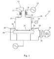
- FIG. 1 depicts a first configuration of apparatus of the invention, shown generally at 10.
- the primary gas feed 12 enters the primary chamber 14 ( ⁇ 7-12cm diameter dielectric cylinder) which has an associated primary ionization source 16.
- An RF antenna 18 nominally 13.56MHz acts as the ICP source. This can be assisted by a DC 20 coil to modify the confinement of the plasma.
- a Faraday shield 21 can be provided between the DC coil 20 and the wall of the primary chamber 14 to reduce capacitive coupling.
- the plasma from the primary source enters the main chamber 22 where the wafer 24 is placed on the wafer support 26, which may be an electrostatic chuck.
- the wafer size could be up to 300mm in standard production applications, although processing of still larger wafers is within the scope of the invention.
- the edge of the wafer 24 is protected by a wafer edge protection (WEP) device 28 to avoid excessive loss of silicon at the wafer edge where the resist edge bead has been removed.
- the main (secondary) chamber 22 has a secondary ionization source 30 having a secondary RF coil 32 placed around the main chamber 22 to provide a secondary plasma close to the chamber wall 22a.
- the RF coil 32 could also operate at 13.56MHz or a lower frequency such as 1-2MHz. It is possible to include a Faraday shield between the secondary RF coil 32 and the wall of the main chamber 22. This can be additional to the Faraday shield 21 positioned adjacent to primary chamber 14.
- the Faraday shield positioned adjacent the main chamber 22 can be instead of the Faraday shield 21, or no Faraday shield may be present.
- An annular gas distribution system 34 is incorporated into the main chamber 22 to provide an independent gas source for the secondary plasma.
- a conductance limiting pathway is introduced at the wafer edge. Gas flows above the WEP 28 and below an annular baffle 36 in a radial fashion to the pump 38 through a gate valve 39. The typical but non-limiting height of this gap is 5-50mm.
- the conductance limiting path can increase the residence time of active gas species at the wafer edge and hence improve process uniformity.
- the WEP is maintained at an elevated temperature to reduce the deposition build up due to successive deposition cycles.
- This heating is preferably achieved by creating a plasma in the chamber 22 to heat all the interior before the wafer of interest is loaded. The plasma during the main process will ensure that the protection system continues to stay at a temperature of 85°C to 150°C.
- This WEP system can have an internal diameter greater than the wafer diameter to ensure that the whole wafer is exposed to the plasma, but material is protected outside the wafer diameter. This material could include the tape and/or frame of a wafer supported by tape or an alternative carrier.
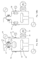
- Figure 2 depicts a second configuration of apparatus of the invention, shown generally at 40. Many of the elements shown in Figure 2 are identical to elements shown in Figure 1 , and identical reference numerals are used to denote such common elements.
- the wafer 24 is carried on a tape 42 and frame 44 arrangement.
- a wafer edge conductance limiting baffle 46 is attached above the wafer position, with an inner diameter close to the diameter of the wafer 24.
- the gap between the wafer 24 (or parts sitting on the wafer support 26 around the wafer 24) should be small enough to cause the etchant gas to mainly interact with the wafer 24 before being pumped around the side of the wafer support 26.
- the gap between the WEP 28 which protects the tape 42 and frame 44 and the baffle 46 is identified by the arrow. A balance must be found between this mixing and the reduced conductance that this causes for pumping the etch products away from the wafer.
- the optimum gap size is often between 15 and 25mm, although other constraints may cause the gap to be 5 to 50mm.
- the baffle is applicable to many etch materials and process gases where a remote plasma source is used, including, but not limited to, Si, GaAs, polymer, Al, and fluorine, chlorine and oxygen based chemistries.
- FIG. 3 shows a) plasma cleaning of the primary chamber 14 and b) plasma cleaning of the primary chamber 22 using apparatus of the invention.
- the apparatus shown in Figure 3 is essentially identical to the apparatus 10 shown in Figure 1 , and identical reference numerals are used to denote common elements.
- the apparatus shown in Figure 3 further comprises a second Faraday shield 54 provided between the secondary RF coil 32 and the wall of the main chamber 22.
- a plasma 50 is produced in the primary chamber 14, and in Figure 3b ) a plasma 52 is produced in the main chamber 22.
- This approach also makes it possible to shift the plasma around by using combination of the sources. More efficient cleaning will yield productivity benefits.
- the invention could be applied to semiconductor wafers, wafers on carriers or wafer in frames.
- the principal adjustment is the positioning of the WEP and the baffle to ensure the conductance limiting path is controlled to improve edge uniformity.
- the WEP would cover the frame and much of the exposed tape but not the wafer edge.
- an alternative means may be used to reduce stray electric coupling, such as a segmented coil.
- a segmented coil Such a coil structure could be mounted inside a chamber, as described in US 6495963 .
- Alternative magnetic plasma confinement means may be used in place of DC coils, and in other embodiments no magnetic plasma confinement means are used at all.
- the frequencies of the RF sources do not have to be the same, and any suitable combination of frequencies might be used. A non-limiting range of possible frequencies is 1-13.56MHz.
Abstract
a first chamber (14) having a first plasma production source (16) and a first gas supply (12) for introducing a supply of gas into the first chamber;
a second chamber (22) having a second plasma production source (30) and a second gas supply (34) for introducing a supply of gas into the second chamber, the second gas supply being independently controllable of the first gas supply;
a workpiece support (26) positioned in the second chamber; and
a plurality of gas flow pathway defining elements for defining a gas flow pathway in the vicinity of the workpiece when positioned on the workpiece support, wherein the gas flow path defining elements include at least one wafer edge region protection element (28) for protecting the edge of the wafer and/or a region outwardly circumjacent to the edge of the wafer, and at least one auxiliary element (36) spaced apart from the wafer edge region protection element to define the gas flow pathway.
Description
- This invention relates to apparatus for processing a semiconductor workpiece.
- Plasma etching is extensively used in the fabrication of semiconductor devices. Cost effective manufacturing of devices requires plasma etch systems to remove the required layers quickly while maintaining the customer specified uniformities (such as etch rate, and selectivity) within and between processed wafers. Frequently there is a compromise to be made between average etch rate and uniformity as in many cases uniformities in the process performance degrade as etch rate is increased.
- High rate anisotropic plasma etching of features in silicon wafers is typically achieved by the "Bosch process" [
US 5501893 ] or cyclic deposition/etch processes [US 8133349 ]. Deposition and etch steps are cyclically carried out in a plasma etch tool to enable a relatively high removal rate of the silicon which is not protected by the mask. This type of process has widespread commercial application and is used to fabricate MEMS (micro electro mechanical systems), gyroscopes, accelerometers, sensors, through silicon vias (TSVs) and even wafer scribing or thinning. In all cases for cost reasons it is desirable to fabricate the part as rapidly as possible and as a consequence a great deal of effort has been applied to developing hardware and processes that enable the high etch rate of silicon. - It should however be understood that process uniformity is also a very important consideration. In most applications a number of parts (die) are patterned over a wafer and amount of material being removed from all parts should be similar. Ideally they should be the same but in practice achieving identical conditions can be very difficult to achieve. Parts at the centre and the edge of the wafer should be processed in a similar fashion if the maximum yield is to be maintained. It is also desirable that etch rate is the same or similar across the whole wafer. If this is not the case some parts will be completed prior to others and in some cases this may prove to be detrimental to the parts that experience over etching. To complicate matters further plasma uniformity may also influence angle of a feature being etched into the masked silicon wafer. Frequently at the edge of the wafer some of the ions hit the wafer surface at less than normal incidence. This results in a slight "tilt" in the anisotropic feature being etched.
US 5683548 describes an ICP reactor where independent control of gas and RF can be applied to a series of concentric channels. By using concentric channels - generally in the same plane - some degree of radial plasma non-uniformity can be reduced near the channels. However, nonuniformities can still exist close to the wafer surface. - The present invention, in at least some of its embodiments, addresses the abovementioned problems.
- According to a first aspect of the invention there is provided an apparatus for processing a semiconductor workpiece including:
- a first chamber having a first plasma production source and a first gas supply for introducing a supply of gas into the first chamber;
- a second chamber having a second plasma production source and a second gas supply for introducing a supply of gas into the second chamber, the second gas supply being independently controllable of the first gas supply;
- a workpiece support positioned in the second chamber; and
- a plurality of gas flow pathway defining elements for defining a gas flow pathway in the vicinity of the workpiece when positioned on the workpiece support, wherein the gas flow path defining elements include at least one wafer edge region protection element for protecting the edge of the wafer and/or a region outwardly circumjacent to the edge of the wafer, and at least one auxiliary element spaced apart from the wafer edge region protection element to define the gas flow pathway.
- The wafer edge region protection device element may be an annular wafer edge protection device.
- The auxiliary element may include one or more baffles. At least one auxiliary element may be an annular baffle.
- The auxiliary element may be positioned over an inner portion of the wafer edge region protection element.
- The auxiliary element may be positioned over an outer part of the wafer edge region protection element.
- The auxiliary element may extend radially inward of the wall of the second chamber.
- The auxiliary element may extend downwardly from the wall of the second chamber.
- The auxiliary element may be spaced apart from the wafer edge region protection element to define a gap of between 2 and 80mm, preferably between 5 and 50mm, most preferably between 15 and 25mm.
- The gas flow pathway may extend radially outwards from the workpiece when positioned on the workpiece support.
- The workpiece, when positioned on the workpiece support, may be supported by a carrier, and the wafer edge region protection element protects the carrier. The carrier may be of the tape and frame kind. The wafer edge protection element may protect the tape and/or the frame.
- The first plasma production source may include an element for coupling energy into the first chamber to maintain a plasma induced in the first chamber, and the second plasma production source may include an element for coupling energy into the second chamber to maintain a plasma induced in the second chamber, wherein the element of the first plasma production source is spaced apart from the element of the second plasma production source so as to decouple the plasma induced in the first chamber from the plasma induced in the second chamber. The apparatus may be configured so that no energy or only insignificant amounts of energy from the element for coupling energy into the first chamber is coupled into the second plasma. Alternatively, or additionally, the apparatus may be configured so that no energy or only insignificant amounts of energy from the element for coupling energy into the second chamber is coupled into the first plasma. In this way, the plasmas may be decoupled. The elements for coupling energy into the first and second chambers may be RF coils. The first chamber may meet the second chamber at an interface having an associated level, and at least one of the elements of the first plasma production source and the elements of the second plasma production source may be spaced apart from said level.
- The skilled reader will appreciate that the auxiliary element is an element which is additional to the wall of the second chamber, although it may project from said wall.
- According to a second aspect of the invention there is provided an apparatus for processing a semiconductor workpiece including;
- a first chamber having a first plasma production source including an element for coupling energy into the first chamber to maintain a plasma induced in the first chamber, and a first gas supply for introducing a supply of gas into the first chamber;
- a second chamber having a second plasma production source including an element for coupling energy into the first chamber to maintain a plasma induced in the second chamber and a second gas supply for introducing a supply of gas into the second chamber, the second gas supply being independently controllable of the first gas supply; and
- a workpiece support positioned in the second chamber;
- wherein the element of the first plasma production source is spaced apart from the element of the second plasma production source so as to decouple the plasma induced in the first chamber from the plasma induced in the second chamber.
- According to a third aspect of the invention there is provided an apparatus for processing a semiconductor workpiece including:
- a chamber having a wall;
- a workpiece support positioned in the chamber;
- at least one plasma production source; and
- a plurality of gas flow pathway defining elements for defining a gas flow pathway in the vicinity of the workpiece when positioned on the workpiece support, wherein the gas flow pathway defining elements include at least one wafer edge region protection element for protecting the edge of the wafer and/or a region outwardly circumjacent to the edge of the wafer, and at least one auxiliary element spaced apart from the wafer edge region protection element to define the gas flow pathway.
- According to a fourth aspect of the invention there is provided a method of cleaning a chamber of an apparatus including the steps of:
- providing an apparatus for processing a semiconductor workpiece according to the first or second aspects of the invention;
- generating a cleaning plasma in the first and/or the second chambers; and
- using the plasma to selectively clean a specific area of the apparatus.
- Whilst the invention has been described above, it extends to any inventive combination of the features set out above, or in the following description, drawings or claims.
- Embodiments of apparatus in accordance with the invention will now be described with reference to the accompanying drawings, in which:-
-
Figure 1 shows a first embodiment of an apparatus of the invention; -
Figure 2 shows a second embodiment of an apparatus of the invention; -
Figure 3 shows plasma cleaning of (a) the second chamber and (b) the first chamber of the apparatus ofFigure 1 ; -
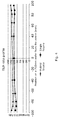
Figure 4 shows normalised etch rate as a function of radial wafer position for a single RF source configuration and a dual RF source configuration; -
Figure 5 shows normalised etch rate as a function of radial wafer position for a single RF source configuration with gas feed and a dual RF source configuration with separate gas feeds; and -
Figure 6 shows etch rate uniformity with and without a gas conductance limiting pathway at the edge of a 200mm blank silicon wafer. - Inductively coupled plasma (ICP) Plasma etch tools frequently use an RF antenna placed around a ceramic bell jar to produce a dense plasma. A central gas feed provides the gas to be disassociated in the bell jar and plasma nonuniformities are reduced through the use of a "diffusion chamber" a large diameter chamber which is placed between the plasma source and the wafer platen assembly. The diffusion chamber allows the plasma to expand to beyond the edge of the wafer. Gas is pumped from the chamber through a gate valve to the bottom of the system. The platen assembly will normally have an electrostatic chuck to aid heat removal from the wafer and an RF bias to aid the etch/deposition process. Although the invention is not limited to ICP plasma etch tools, for the purposes of illustration the invention will now be described in relation to etch tools of this type.
- In the context of RF based, ICP plasma etch tools described in the accompanying drawings, features of the invention are as follows: a) two concentric RF sources, the primary source being located in the upper bell jar and the diameter of this jar being lower than that of the main chamber; b) two gas feeds, one to the primary source and the other being an annular arrangement to the upper part of the main chamber; and c) a conductance limiting path at the edge of the wafer to reduce the flow of gas at the wafer edge.
- By judicious control of one or more of these factors, etch rate can be enhanced while uniformity can be maintained at acceptable levels. These features can be seen diagrammatically in
Figure 1 . - A secondary benefit of the invention is an improved plasma clean process capability. Plasma clean processes can be used to remove deposited material from the chamber walls. This is a very important factor which must be controlled to maintain wafer - wafer uniformity over time. An advantage of the present invention is that because the two plasma sources can be operated independently the operator can run clean regimes targeting specific areas of the chamber, (ICP only for main reaction chamber / high density plasma only for bell jar). The invention also makes it possible to shift the plasma around by using combination of the sources. More efficient cleaning will yield productivity benefits.
-
Figure 1 depicts a first configuration of apparatus of the invention, shown generally at 10. Theprimary gas feed 12 enters the primary chamber 14 (∼7-12cm diameter dielectric cylinder) which has an associatedprimary ionization source 16. AnRF antenna 18 nominally 13.56MHz acts as the ICP source. This can be assisted by aDC 20 coil to modify the confinement of the plasma. AFaraday shield 21 can be provided between theDC coil 20 and the wall of theprimary chamber 14 to reduce capacitive coupling. The plasma from the primary source enters themain chamber 22 where thewafer 24 is placed on thewafer support 26, which may be an electrostatic chuck. The wafer size could be up to 300mm in standard production applications, although processing of still larger wafers is within the scope of the invention. The edge of thewafer 24 is protected by a wafer edge protection (WEP)device 28 to avoid excessive loss of silicon at the wafer edge where the resist edge bead has been removed. The main (secondary)chamber 22 has asecondary ionization source 30 having asecondary RF coil 32 placed around themain chamber 22 to provide a secondary plasma close to the chamber wall 22a. TheRF coil 32 could also operate at 13.56MHz or a lower frequency such as 1-2MHz. It is possible to include a Faraday shield between thesecondary RF coil 32 and the wall of themain chamber 22. This can be additional to theFaraday shield 21 positioned adjacent toprimary chamber 14. Alternatively, the Faraday shield positioned adjacent themain chamber 22 can be instead of theFaraday shield 21, or no Faraday shield may be present. An annulargas distribution system 34 is incorporated into themain chamber 22 to provide an independent gas source for the secondary plasma. A conductance limiting pathway is introduced at the wafer edge. Gas flows above theWEP 28 and below anannular baffle 36 in a radial fashion to thepump 38 through agate valve 39. The typical but non-limiting height of this gap is 5-50mm. The conductance limiting path can increase the residence time of active gas species at the wafer edge and hence improve process uniformity. - It is desirable that the WEP is maintained at an elevated temperature to reduce the deposition build up due to successive deposition cycles. This heating is preferably achieved by creating a plasma in the
chamber 22 to heat all the interior before the wafer of interest is loaded. The plasma during the main process will ensure that the protection system continues to stay at a temperature of 85°C to 150°C. This WEP system can have an internal diameter greater than the wafer diameter to ensure that the whole wafer is exposed to the plasma, but material is protected outside the wafer diameter. This material could include the tape and/or frame of a wafer supported by tape or an alternative carrier. Such a configuration is shown inFigure 2. Figure 2 depicts a second configuration of apparatus of the invention, shown generally at 40. Many of the elements shown inFigure 2 are identical to elements shown inFigure 1 , and identical reference numerals are used to denote such common elements. - In
Figure 2 thewafer 24 is carried on atape 42 andframe 44 arrangement. A wafer edgeconductance limiting baffle 46 is attached above the wafer position, with an inner diameter close to the diameter of thewafer 24. The gap between the wafer 24 (or parts sitting on thewafer support 26 around the wafer 24) should be small enough to cause the etchant gas to mainly interact with thewafer 24 before being pumped around the side of thewafer support 26. InFigure 2 the gap between theWEP 28 which protects thetape 42 andframe 44 and thebaffle 46 is identified by the arrow. A balance must be found between this mixing and the reduced conductance that this causes for pumping the etch products away from the wafer. As a guideline, the optimum gap size is often between 15 and 25mm, although other constraints may cause the gap to be 5 to 50mm. The baffle is applicable to many etch materials and process gases where a remote plasma source is used, including, but not limited to, Si, GaAs, polymer, Al, and fluorine, chlorine and oxygen based chemistries. - Cleaning the process chamber following an etch cycle or number of wafers is essential if process reproducibility is to be maintained over time. Plasma clean processes can be used to remove deposited material from the chamber walls and in turn increase the time between venting the chamber for a maintenance clean. The present invention provides apparatus having two plasma sources which can be operated independently, enabling specific clean regimes to be implemented which target specific areas of the chambers (ICP only for main chamber / high density plasma only for bell jar (primary chamber)).
Figure 3 shows a) plasma cleaning of theprimary chamber 14 and b) plasma cleaning of theprimary chamber 22 using apparatus of the invention. The apparatus shown inFigure 3 is essentially identical to theapparatus 10 shown inFigure 1 , and identical reference numerals are used to denote common elements. The apparatus shown inFigure 3 further comprises asecond Faraday shield 54 provided between thesecondary RF coil 32 and the wall of themain chamber 22. InFigure 3a ) aplasma 50 is produced in theprimary chamber 14, and inFigure 3b ) aplasma 52 is produced in themain chamber 22. This approach also makes it possible to shift the plasma around by using combination of the sources. More efficient cleaning will yield productivity benefits. - By using two independent sources - one primary source at the top of the chamber in a small ceramic / insulating container where the principal dissociation of the reactive gases will take place - and secondary auxiliary source between the primary source and the wafer - ideally close to the wafer - radial non- uniformities close to the wafer edge can be compensated by the auxiliary source. When using a single source the plasma density at the centre of the process chamber tends to be higher than at the edge. This is particularly pronounced using a small diameter tube as the first chamber. As the RF power applied to the antenna is increased, the non-uniformity can be increased. In
Figure 4 we can see not only improved uniformity for 200mm wafers but also higher normalised etch rate due to the use of the secondary RF source. The RF power for the primary source was maintained a 3kW for both sets of data but 1.5kW power was used in the secondary source for the "hybrid source" measurements. Gas was only supplied to the primary source. - The benefit of having an independent annular gas supply to the secondary RF source can be seen in
Figure 5 . Here the normalized etch rate for a 300mm wafer can be seen gas flow solely to the primary source and when gas is supplied with a ratio of 2:1 between the primary and secondary sources. Increasing the gas low to the annular gas supply to the main chamber improves the uniformity of the plasma and in turn improves etch uniformity. - In
Figure 6 we can see the benefit of utilizing a conductance limiting path (baffle/WEP channel) at the edge of the wafer. Uniformity can be improved by reducing the depletion of reactive species at the wafer periphery and reducing the number of ions. This improves the uniformity across the wafer and therefore also allows a higher etch rate for a given uniformity by adjusting other process parameters which would normally worsen the uniformity. - The invention could be applied to semiconductor wafers, wafers on carriers or wafer in frames. The principal adjustment is the positioning of the WEP and the baffle to ensure the conductance limiting path is controlled to improve edge uniformity. In the case of wafers in frames the WEP would cover the frame and much of the exposed tape but not the wafer edge.
- Numerous variations to the specific embodiments described above are within the scope of the invention. For example, instead of using Faraday shields, an alternative means may be used to reduce stray electric coupling, such as a segmented coil. Such a coil structure could be mounted inside a chamber, as described in
US 6495963 . Alternative magnetic plasma confinement means may be used in place of DC coils, and in other embodiments no magnetic plasma confinement means are used at all. The frequencies of the RF sources do not have to be the same, and any suitable combination of frequencies might be used. A non-limiting range of possible frequencies is 1-13.56MHz.
Claims (15)
- An apparatus for processing a semiconductor workpiece including:a first chamber having a first plasma production source and a first gas supply for introducing a supply of gas into the first chamber;a second chamber having a second plasma production source and a second gas supply for introducing a supply of gas into the second chamber, the second gas supply being independently controllable of the first gas supply;a workpiece support positioned in the second chamber; anda plurality of gas flow pathway defining elements for defining a gas flow pathway in the vicinity of the workpiece when positioned on the workpiece support, wherein the gas flow path defining elements include at least one wafer edge region protection element for protecting the edge of the wafer and/or a region outwardly circumjacent to the edge of the wafer, and at least one auxiliary element spaced apart from the wafer edge region protection element to define the gas flow pathway.
- An apparatus according to claim 1 in which the wafer edge region protection device element is an annular wafer edge protection device.
- An apparatus according to claim 1 or claim 2 in which the at least one auxiliary element includes one or more baffles.
- An apparatus according to claim 3 at which the at least one auxiliary element is an annular baffle.
- An apparatus according to any previous claim in which the auxiliary element is positioned over an inner portion of the wafer edge region protection element.
- An apparatus according to any one of claims 1 to 4 in which the auxiliary element is positioned over an outer part of the wafer edge region protection element.
- An apparatus according to any previous claim in which the auxiliary element extends radially inward of the wall of the second chamber.
- An apparatus according to any one of claims 1 to 6 in which the auxiliary element extends downwardly from the wall of the second chamber.
- An apparatus according to any previous claim in which the auxiliary element is spaced apart from the wafer edge region protection element to define a gap of between 2 and 80mm, preferably between 5 and 50mm, most preferably between 15 and 25mm.
- An apparatus according to any previous claim in which the gas flow pathway extends radially outwards from the workpiece when positioned on the workpiece support.
- An apparatus according to any previous claim in which the workpiece, when positioned on the workpiece support, is supported by a carrier, and the wafer edge region protection element protects the carrier.
- An apparatus according to claim 11 in which the carrier is of the tape and frame kind, and the wafer edge protection element protects the tape and/or the frame.
- An apparatus according to any previous claim in which the first plasma production source includes an element for coupling energy into the first chamber to maintain a plasma induced in the first chamber, and the second plasma production source includes an element for coupling energy into the second chamber to maintain a plasma induced in the second chamber, wherein the element of the first plasma production source is spaced apart from the element of the second plasma production source so as to decouple the plasma induced in the first chamber from the plasma induced in the second chamber.
- An apparatus according to claim 13 in which the first chamber meets the second chamber at an interface having an associated level, and at least one of the elements of the first plasma production source and the elements of the second plasma production source is spaced apart from said level.
- An apparatus for processing a semiconductor workpiece including:a chamber having a wall;a workpiece support positioned in the chamber;at least one plasma production source; anda plurality of gas flow pathway defining elements for defining a gas flow pathway in the vicinity of the workpiece when positioned on the workpiece support, wherein the gas flow pathway defining elements include at least one wafer edge region protection element for protecting the edge of the wafer and/or a region outwardly circumjacent to the edge of the wafer, and at least one auxiliary element spaced apart from the wafer edge region protection element to define the gas flow pathway.
Applications Claiming Priority (1)
| Application Number | Priority Date | Filing Date | Title |
|---|---|---|---|
| GBGB1309583.1A GB201309583D0 (en) | 2013-05-29 | 2013-05-29 | Apparatus for processing a semiconductor workpiece |
Publications (2)
| Publication Number | Publication Date |
|---|---|
| EP2808886A1 true EP2808886A1 (en) | 2014-12-03 |
| EP2808886B1 EP2808886B1 (en) | 2020-10-21 |
Family
ID=48784848
Family Applications (1)
| Application Number | Title | Priority Date | Filing Date |
|---|---|---|---|
| EP14275128.8A Active EP2808886B1 (en) | 2013-05-29 | 2014-05-27 | Apparatus for processing a semiconductor workpiece |
Country Status (7)
| Country | Link |
|---|---|
| US (1) | US20140352889A1 (en) |
| EP (1) | EP2808886B1 (en) |
| JP (2) | JP6559932B2 (en) |
| KR (1) | KR102244575B1 (en) |
| CN (1) | CN104217943B (en) |
| GB (1) | GB201309583D0 (en) |
| TW (1) | TWI654645B (en) |
Families Citing this family (7)
| Publication number | Priority date | Publication date | Assignee | Title |
|---|---|---|---|---|
| DE102014216195A1 (en) * | 2014-08-14 | 2016-02-18 | Robert Bosch Gmbh | Apparatus for anisotropically etching a substrate and method for operating an apparatus for anisotropic etching of a substrate |
| JP6296297B2 (en) * | 2014-08-27 | 2018-03-20 | パナソニックIpマネジメント株式会社 | Plasma processing apparatus and plasma processing method |
| KR101680850B1 (en) * | 2016-06-28 | 2016-11-29 | 주식회사 기가레인 | Plasma processing apparatus having control of exhaust flow path size |
| CN108155080A (en) * | 2016-12-02 | 2018-06-12 | 北京北方华创微电子装备有限公司 | Plasma generating device and the semiconductor equipment including the device |
| CN108155093A (en) * | 2016-12-02 | 2018-06-12 | 北京北方华创微电子装备有限公司 | Plasma generating device and the semiconductor equipment comprising the device |
| JP6750534B2 (en) * | 2017-02-24 | 2020-09-02 | 東京エレクトロン株式会社 | Film deposition equipment |
| CN111508802B (en) * | 2020-04-22 | 2023-10-13 | 北京北方华创微电子装备有限公司 | Reaction chamber and etching method thereof |
Citations (9)
| Publication number | Priority date | Publication date | Assignee | Title |
|---|---|---|---|---|
| US5501893A (en) | 1992-12-05 | 1996-03-26 | Robert Bosch Gmbh | Method of anisotropically etching silicon |
| US5683548A (en) | 1996-02-22 | 1997-11-04 | Motorola, Inc. | Inductively coupled plasma reactor and process |
| US6495963B1 (en) | 1998-12-17 | 2002-12-17 | Trikon Holdings Limited | Inductive coil assembly having multiple coil segments for plasma processing apparatus |
| US20090142929A1 (en) * | 2007-11-29 | 2009-06-04 | Tokyo Electron Limited | Method for plasma processing over wide pressure range |
| US20110177694A1 (en) * | 2010-01-15 | 2011-07-21 | Tokyo Electron Limited | Switchable Neutral Beam Source |
| US20120024479A1 (en) * | 2010-07-30 | 2012-02-02 | Applied Materials, Inc. | Apparatus for controlling the flow of a gas in a process chamber |
| US8133349B1 (en) | 2010-11-03 | 2012-03-13 | Lam Research Corporation | Rapid and uniform gas switching for a plasma etch process |
| US20120244684A1 (en) * | 2011-03-24 | 2012-09-27 | Kunihiko Suzuki | Film-forming apparatus and method |
| US20120285622A1 (en) * | 2011-05-09 | 2012-11-15 | Lim Ji Man | Plasma device |
Family Cites Families (27)
| Publication number | Priority date | Publication date | Assignee | Title |
|---|---|---|---|---|
| US3650042A (en) * | 1969-05-19 | 1972-03-21 | Ibm | Gas barrier for interconnecting and isolating two atmospheres |
| JPS5972718A (en) * | 1982-10-20 | 1984-04-24 | Toshiba Corp | Vertical vapor phase growth device |
| US5173336A (en) * | 1991-01-22 | 1992-12-22 | Santa Barbara Research Center | Metal organic chemical vapor deposition (MOCVD) reactor with recirculation suppressing flow guide |
| JP3323530B2 (en) * | 1991-04-04 | 2002-09-09 | 株式会社日立製作所 | Method for manufacturing semiconductor device |
| JPH0689880A (en) * | 1992-09-08 | 1994-03-29 | Tokyo Electron Ltd | Etching equipment |
| US5744049A (en) * | 1994-07-18 | 1998-04-28 | Applied Materials, Inc. | Plasma reactor with enhanced plasma uniformity by gas addition, and method of using same |
| TW434745B (en) * | 1995-06-07 | 2001-05-16 | Tokyo Electron Ltd | Plasma processing apparatus |
| JP3585606B2 (en) * | 1995-09-19 | 2004-11-04 | アネルバ株式会社 | Electrode device of CVD equipment |
| US5891348A (en) * | 1996-01-26 | 1999-04-06 | Applied Materials, Inc. | Process gas focusing apparatus and method |
| JPH10172954A (en) * | 1996-12-06 | 1998-06-26 | Hitachi Ltd | Plasma processor |
| JP3483725B2 (en) * | 1997-04-02 | 2004-01-06 | 株式会社日立製作所 | Plasma processing apparatus and processing method |
| US6149730A (en) * | 1997-10-08 | 2000-11-21 | Nec Corporation | Apparatus for forming films of a semiconductor device, a method of manufacturing a semiconductor device, and a method of forming thin films of a semiconductor |
| JP2001308077A (en) * | 2000-04-27 | 2001-11-02 | Toshiba Corp | Semiconductor device manufacturing apparatus |
| US20020185226A1 (en) * | 2000-08-10 | 2002-12-12 | Lea Leslie Michael | Plasma processing apparatus |
| US6602381B1 (en) * | 2001-04-30 | 2003-08-05 | Lam Research Corporation | Plasma confinement by use of preferred RF return path |
| GB0323001D0 (en) * | 2003-10-01 | 2003-11-05 | Oxford Instr Plasma Technology | Apparatus and method for plasma treating a substrate |
| JP4972277B2 (en) * | 2004-11-10 | 2012-07-11 | 東京エレクトロン株式会社 | Substrate processing apparatus recovery method, apparatus recovery program, and substrate processing apparatus |
| WO2008007944A1 (en) * | 2006-07-12 | 2008-01-17 | Technische Universiteit Eindhoven | Method and device for treating a substrate by means of a plasma |
| KR100927375B1 (en) * | 2007-09-04 | 2009-11-19 | 주식회사 유진테크 | Exhaust unit, exhaust control method using same, substrate processing apparatus including the exhaust unit |
| JP5256866B2 (en) * | 2008-02-05 | 2013-08-07 | 東京エレクトロン株式会社 | Processing equipment |
| US8262800B1 (en) * | 2008-02-12 | 2012-09-11 | Novellus Systems, Inc. | Methods and apparatus for cleaning deposition reactors |
| KR100999588B1 (en) * | 2008-03-25 | 2010-12-08 | 주식회사 유진테크 | Apparatus and method for processing substrate |
| JP4855506B2 (en) * | 2009-09-15 | 2012-01-18 | 住友精密工業株式会社 | Plasma etching equipment |
| JP5445252B2 (en) * | 2010-03-16 | 2014-03-19 | 東京エレクトロン株式会社 | Deposition equipment |
| US9404180B2 (en) * | 2010-03-16 | 2016-08-02 | Tokyo Electron Limited | Deposition device |
| US8802545B2 (en) * | 2011-03-14 | 2014-08-12 | Plasma-Therm Llc | Method and apparatus for plasma dicing a semi-conductor wafer |
| JP5886821B2 (en) * | 2013-01-04 | 2016-03-16 | ピーエスケー インコーポレイテッド | Substrate processing apparatus and method |
-
2013
- 2013-05-29 GB GBGB1309583.1A patent/GB201309583D0/en not_active Ceased
-
2014
- 2014-05-23 US US14/285,730 patent/US20140352889A1/en not_active Abandoned
- 2014-05-27 EP EP14275128.8A patent/EP2808886B1/en active Active
- 2014-05-28 TW TW103118610A patent/TWI654645B/en active
- 2014-05-29 JP JP2014110917A patent/JP6559932B2/en active Active
- 2014-05-29 CN CN201410234927.1A patent/CN104217943B/en active Active
- 2014-05-29 KR KR1020140065073A patent/KR102244575B1/en active IP Right Grant
-
2019
- 2019-04-04 JP JP2019072189A patent/JP2019110346A/en not_active Withdrawn
Patent Citations (9)
| Publication number | Priority date | Publication date | Assignee | Title |
|---|---|---|---|---|
| US5501893A (en) | 1992-12-05 | 1996-03-26 | Robert Bosch Gmbh | Method of anisotropically etching silicon |
| US5683548A (en) | 1996-02-22 | 1997-11-04 | Motorola, Inc. | Inductively coupled plasma reactor and process |
| US6495963B1 (en) | 1998-12-17 | 2002-12-17 | Trikon Holdings Limited | Inductive coil assembly having multiple coil segments for plasma processing apparatus |
| US20090142929A1 (en) * | 2007-11-29 | 2009-06-04 | Tokyo Electron Limited | Method for plasma processing over wide pressure range |
| US20110177694A1 (en) * | 2010-01-15 | 2011-07-21 | Tokyo Electron Limited | Switchable Neutral Beam Source |
| US20120024479A1 (en) * | 2010-07-30 | 2012-02-02 | Applied Materials, Inc. | Apparatus for controlling the flow of a gas in a process chamber |
| US8133349B1 (en) | 2010-11-03 | 2012-03-13 | Lam Research Corporation | Rapid and uniform gas switching for a plasma etch process |
| US20120244684A1 (en) * | 2011-03-24 | 2012-09-27 | Kunihiko Suzuki | Film-forming apparatus and method |
| US20120285622A1 (en) * | 2011-05-09 | 2012-11-15 | Lim Ji Man | Plasma device |
Non-Patent Citations (1)
| Title |
|---|
| DAVID BUTLER: "Production Solutions for Via Reveal", EUROPEAN 3D TSV SUMMIT 2013, 22 January 2013 (2013-01-22), XP055135425, Retrieved from the Internet <URL:http://www.semi.org/eu/sites/semi.org/files/docs/David_Butler%20Production%20solutions%20for%20via%20reveal%20publish.pdf> [retrieved on 20140819] * |
Also Published As
| Publication number | Publication date |
|---|---|
| TW201511069A (en) | 2015-03-16 |
| JP2014232877A (en) | 2014-12-11 |
| CN104217943A (en) | 2014-12-17 |
| US20140352889A1 (en) | 2014-12-04 |
| CN104217943B (en) | 2020-03-06 |
| TWI654645B (en) | 2019-03-21 |
| GB201309583D0 (en) | 2013-07-10 |
| JP6559932B2 (en) | 2019-08-14 |
| KR102244575B1 (en) | 2021-04-23 |
| JP2019110346A (en) | 2019-07-04 |
| KR20140140514A (en) | 2014-12-09 |
| EP2808886B1 (en) | 2020-10-21 |
Similar Documents
| Publication | Publication Date | Title |
|---|---|---|
| EP2808886B1 (en) | Apparatus for processing a semiconductor workpiece | |
| US9443753B2 (en) | Apparatus for controlling the flow of a gas in a process chamber | |
| JP6646953B2 (en) | Ceramic showerhead including central gas injector for adjustable convection-diffusion gas flow in semiconductor substrate processing equipment | |
| US9997381B2 (en) | Hybrid edge ring for plasma wafer processing | |
| CN107564793B (en) | Power deposition control in Inductively Coupled Plasma (ICP) reactors | |
| US9171702B2 (en) | Consumable isolation ring for movable substrate support assembly of a plasma processing chamber | |
| US8840725B2 (en) | Chamber with uniform flow and plasma distribution | |
| US20170301578A1 (en) | Focus ring assembly and a method of processing a substrate using the same | |
| CN110249416B (en) | Plasma density control at substrate edge | |
| CN110546733B (en) | Preventing material deposition on a workpiece in a processing chamber | |
| WO2009089244A1 (en) | Showerhead insulator and etch chamber liner | |
| US20150102011A1 (en) | Plasma etching apparatus | |
| KR20200070118A (en) | Apparatus and method to reduce polymers deposition | |
| CN105632861A (en) | Inductively-coupled plasma processing device and plasma etching method | |
| KR20200101993A (en) | Process kit for substrate support | |
| KR20190070228A (en) | Shower Head Structure and Apparatus for Processing Semiconductor Substrate Including The Same | |
| CN115280464A (en) | Low resistance confinement liner for use in a plasma chamber | |
| US20180294139A1 (en) | Gas phase particle reduction in pecvd chamber | |
| KR20180072916A (en) | Apparatus for treating substrate | |
| KR101098793B1 (en) | Adaptively plasma source and plasma chamber for processing a large-diameter wafer | |
| EP2863411B1 (en) | Plasma etching apparatus | |
| WO2014088779A1 (en) | Deposition shield for plasma enhanced substrate processing | |
| KR20210154275A (en) | Stray Plasma Protection Device for Substrate Process Chamber | |
| CN115461837A (en) | High conductivity process kit | |
| KR20100001652A (en) | Focus ring of dry etch device |
Legal Events
| Date | Code | Title | Description |
|---|---|---|---|
| PUAI | Public reference made under article 153(3) epc to a published international application that has entered the european phase |
Free format text: ORIGINAL CODE: 0009012 |
|
| 17P | Request for examination filed |
Effective date: 20140527 |
|
| AK | Designated contracting states |
Kind code of ref document: A1 Designated state(s): AL AT BE BG CH CY CZ DE DK EE ES FI FR GB GR HR HU IE IS IT LI LT LU LV MC MK MT NL NO PL PT RO RS SE SI SK SM TR |
|
| AX | Request for extension of the european patent |
Extension state: BA ME |
|
| R17P | Request for examination filed (corrected) |
Effective date: 20150602 |
|
| RBV | Designated contracting states (corrected) |
Designated state(s): AL AT BE BG CH CY CZ DE DK EE ES FI FR GB GR HR HU IE IS IT LI LT LU LV MC MK MT NL NO PL PT RO RS SE SI SK SM TR |
|
| 111Z | Information provided on other rights and legal means of execution |
Free format text: AL AT BE BG CH CY CZ DE DK EE ES FI FR GB GR HR HU IE IS IT LT LU LV MC MK MT NL NO PL PT RO RS SE SI SK SM TR Effective date: 20150702 |
|
| D11X | Information provided on other rights and legal means of execution (deleted) | ||
| STAA | Information on the status of an ep patent application or granted ep patent |
Free format text: STATUS: EXAMINATION IS IN PROGRESS |
|
| 17Q | First examination report despatched |
Effective date: 20200327 |
|
| GRAP | Despatch of communication of intention to grant a patent |
Free format text: ORIGINAL CODE: EPIDOSNIGR1 |
|
| STAA | Information on the status of an ep patent application or granted ep patent |
Free format text: STATUS: GRANT OF PATENT IS INTENDED |
|
| INTG | Intention to grant announced |
Effective date: 20200511 |
|
| GRAS | Grant fee paid |
Free format text: ORIGINAL CODE: EPIDOSNIGR3 |
|
| GRAA | (expected) grant |
Free format text: ORIGINAL CODE: 0009210 |
|
| STAA | Information on the status of an ep patent application or granted ep patent |
Free format text: STATUS: THE PATENT HAS BEEN GRANTED |
|
| AK | Designated contracting states |
Kind code of ref document: B1 Designated state(s): AL AT BE BG CH CY CZ DE DK EE ES FI FR GB GR HR HU IE IS IT LI LT LU LV MC MK MT NL NO PL PT RO RS SE SI SK SM TR |
|
| REG | Reference to a national code |
Ref country code: GB Ref legal event code: FG4D |
|
| REG | Reference to a national code |
Ref country code: CH Ref legal event code: EP |
|
| REG | Reference to a national code |
Ref country code: DE Ref legal event code: R096 Ref document number: 602014071404 Country of ref document: DE |
|
| REG | Reference to a national code |
Ref country code: IE Ref legal event code: FG4D |
|
| REG | Reference to a national code |
Ref country code: AT Ref legal event code: REF Ref document number: 1326704 Country of ref document: AT Kind code of ref document: T Effective date: 20201115 |
|
| REG | Reference to a national code |
Ref country code: AT Ref legal event code: MK05 Ref document number: 1326704 Country of ref document: AT Kind code of ref document: T Effective date: 20201021 |
|
| REG | Reference to a national code |
Ref country code: NL Ref legal event code: MP Effective date: 20201021 |
|
| PG25 | Lapsed in a contracting state [announced via postgrant information from national office to epo] |
Ref country code: GR Free format text: LAPSE BECAUSE OF FAILURE TO SUBMIT A TRANSLATION OF THE DESCRIPTION OR TO PAY THE FEE WITHIN THE PRESCRIBED TIME-LIMIT Effective date: 20210122 Ref country code: RS Free format text: LAPSE BECAUSE OF FAILURE TO SUBMIT A TRANSLATION OF THE DESCRIPTION OR TO PAY THE FEE WITHIN THE PRESCRIBED TIME-LIMIT Effective date: 20201021 Ref country code: FI Free format text: LAPSE BECAUSE OF FAILURE TO SUBMIT A TRANSLATION OF THE DESCRIPTION OR TO PAY THE FEE WITHIN THE PRESCRIBED TIME-LIMIT Effective date: 20201021 Ref country code: NO Free format text: LAPSE BECAUSE OF FAILURE TO SUBMIT A TRANSLATION OF THE DESCRIPTION OR TO PAY THE FEE WITHIN THE PRESCRIBED TIME-LIMIT Effective date: 20210121 Ref country code: NL Free format text: LAPSE BECAUSE OF FAILURE TO SUBMIT A TRANSLATION OF THE DESCRIPTION OR TO PAY THE FEE WITHIN THE PRESCRIBED TIME-LIMIT Effective date: 20201021 Ref country code: PT Free format text: LAPSE BECAUSE OF FAILURE TO SUBMIT A TRANSLATION OF THE DESCRIPTION OR TO PAY THE FEE WITHIN THE PRESCRIBED TIME-LIMIT Effective date: 20210222 |
|
| REG | Reference to a national code |
Ref country code: LT Ref legal event code: MG4D |
|
| PG25 | Lapsed in a contracting state [announced via postgrant information from national office to epo] |
Ref country code: IS Free format text: LAPSE BECAUSE OF FAILURE TO SUBMIT A TRANSLATION OF THE DESCRIPTION OR TO PAY THE FEE WITHIN THE PRESCRIBED TIME-LIMIT Effective date: 20210221 Ref country code: LV Free format text: LAPSE BECAUSE OF FAILURE TO SUBMIT A TRANSLATION OF THE DESCRIPTION OR TO PAY THE FEE WITHIN THE PRESCRIBED TIME-LIMIT Effective date: 20201021 Ref country code: SE Free format text: LAPSE BECAUSE OF FAILURE TO SUBMIT A TRANSLATION OF THE DESCRIPTION OR TO PAY THE FEE WITHIN THE PRESCRIBED TIME-LIMIT Effective date: 20201021 Ref country code: PL Free format text: LAPSE BECAUSE OF FAILURE TO SUBMIT A TRANSLATION OF THE DESCRIPTION OR TO PAY THE FEE WITHIN THE PRESCRIBED TIME-LIMIT Effective date: 20201021 Ref country code: AT Free format text: LAPSE BECAUSE OF FAILURE TO SUBMIT A TRANSLATION OF THE DESCRIPTION OR TO PAY THE FEE WITHIN THE PRESCRIBED TIME-LIMIT Effective date: 20201021 Ref country code: ES Free format text: LAPSE BECAUSE OF FAILURE TO SUBMIT A TRANSLATION OF THE DESCRIPTION OR TO PAY THE FEE WITHIN THE PRESCRIBED TIME-LIMIT Effective date: 20201021 Ref country code: BG Free format text: LAPSE BECAUSE OF FAILURE TO SUBMIT A TRANSLATION OF THE DESCRIPTION OR TO PAY THE FEE WITHIN THE PRESCRIBED TIME-LIMIT Effective date: 20210121 |
|
| PG25 | Lapsed in a contracting state [announced via postgrant information from national office to epo] |
Ref country code: HR Free format text: LAPSE BECAUSE OF FAILURE TO SUBMIT A TRANSLATION OF THE DESCRIPTION OR TO PAY THE FEE WITHIN THE PRESCRIBED TIME-LIMIT Effective date: 20201021 |
|
| REG | Reference to a national code |
Ref country code: DE Ref legal event code: R097 Ref document number: 602014071404 Country of ref document: DE |
|
| PG25 | Lapsed in a contracting state [announced via postgrant information from national office to epo] |
Ref country code: RO Free format text: LAPSE BECAUSE OF FAILURE TO SUBMIT A TRANSLATION OF THE DESCRIPTION OR TO PAY THE FEE WITHIN THE PRESCRIBED TIME-LIMIT Effective date: 20201021 Ref country code: SK Free format text: LAPSE BECAUSE OF FAILURE TO SUBMIT A TRANSLATION OF THE DESCRIPTION OR TO PAY THE FEE WITHIN THE PRESCRIBED TIME-LIMIT Effective date: 20201021 Ref country code: LT Free format text: LAPSE BECAUSE OF FAILURE TO SUBMIT A TRANSLATION OF THE DESCRIPTION OR TO PAY THE FEE WITHIN THE PRESCRIBED TIME-LIMIT Effective date: 20201021 Ref country code: EE Free format text: LAPSE BECAUSE OF FAILURE TO SUBMIT A TRANSLATION OF THE DESCRIPTION OR TO PAY THE FEE WITHIN THE PRESCRIBED TIME-LIMIT Effective date: 20201021 Ref country code: CZ Free format text: LAPSE BECAUSE OF FAILURE TO SUBMIT A TRANSLATION OF THE DESCRIPTION OR TO PAY THE FEE WITHIN THE PRESCRIBED TIME-LIMIT Effective date: 20201021 Ref country code: SM Free format text: LAPSE BECAUSE OF FAILURE TO SUBMIT A TRANSLATION OF THE DESCRIPTION OR TO PAY THE FEE WITHIN THE PRESCRIBED TIME-LIMIT Effective date: 20201021 |
|
| PLBE | No opposition filed within time limit |
Free format text: ORIGINAL CODE: 0009261 |
|
| STAA | Information on the status of an ep patent application or granted ep patent |
Free format text: STATUS: NO OPPOSITION FILED WITHIN TIME LIMIT |
|
| PG25 | Lapsed in a contracting state [announced via postgrant information from national office to epo] |
Ref country code: DK Free format text: LAPSE BECAUSE OF FAILURE TO SUBMIT A TRANSLATION OF THE DESCRIPTION OR TO PAY THE FEE WITHIN THE PRESCRIBED TIME-LIMIT Effective date: 20201021 |
|
| 26N | No opposition filed |
Effective date: 20210722 |
|
| PG25 | Lapsed in a contracting state [announced via postgrant information from national office to epo] |
Ref country code: AL Free format text: LAPSE BECAUSE OF FAILURE TO SUBMIT A TRANSLATION OF THE DESCRIPTION OR TO PAY THE FEE WITHIN THE PRESCRIBED TIME-LIMIT Effective date: 20201021 Ref country code: IT Free format text: LAPSE BECAUSE OF FAILURE TO SUBMIT A TRANSLATION OF THE DESCRIPTION OR TO PAY THE FEE WITHIN THE PRESCRIBED TIME-LIMIT Effective date: 20201021 |
|
| PG25 | Lapsed in a contracting state [announced via postgrant information from national office to epo] |
Ref country code: SI Free format text: LAPSE BECAUSE OF FAILURE TO SUBMIT A TRANSLATION OF THE DESCRIPTION OR TO PAY THE FEE WITHIN THE PRESCRIBED TIME-LIMIT Effective date: 20201021 |
|
| REG | Reference to a national code |
Ref country code: CH Ref legal event code: PL |
|
| PG25 | Lapsed in a contracting state [announced via postgrant information from national office to epo] |
Ref country code: MC Free format text: LAPSE BECAUSE OF FAILURE TO SUBMIT A TRANSLATION OF THE DESCRIPTION OR TO PAY THE FEE WITHIN THE PRESCRIBED TIME-LIMIT Effective date: 20201021 Ref country code: LI Free format text: LAPSE BECAUSE OF NON-PAYMENT OF DUE FEES Effective date: 20210531 Ref country code: LU Free format text: LAPSE BECAUSE OF NON-PAYMENT OF DUE FEES Effective date: 20210527 Ref country code: CH Free format text: LAPSE BECAUSE OF NON-PAYMENT OF DUE FEES Effective date: 20210531 |
|
| REG | Reference to a national code |
Ref country code: BE Ref legal event code: MM Effective date: 20210531 |
|
| PG25 | Lapsed in a contracting state [announced via postgrant information from national office to epo] |
Ref country code: IE Free format text: LAPSE BECAUSE OF NON-PAYMENT OF DUE FEES Effective date: 20210527 |
|
| PG25 | Lapsed in a contracting state [announced via postgrant information from national office to epo] |
Ref country code: IS Free format text: LAPSE BECAUSE OF FAILURE TO SUBMIT A TRANSLATION OF THE DESCRIPTION OR TO PAY THE FEE WITHIN THE PRESCRIBED TIME-LIMIT Effective date: 20210221 |
|
| PG25 | Lapsed in a contracting state [announced via postgrant information from national office to epo] |
Ref country code: BE Free format text: LAPSE BECAUSE OF NON-PAYMENT OF DUE FEES Effective date: 20210531 |
|
| PG25 | Lapsed in a contracting state [announced via postgrant information from national office to epo] |
Ref country code: HU Free format text: LAPSE BECAUSE OF FAILURE TO SUBMIT A TRANSLATION OF THE DESCRIPTION OR TO PAY THE FEE WITHIN THE PRESCRIBED TIME-LIMIT; INVALID AB INITIO Effective date: 20140527 |
|
| PG25 | Lapsed in a contracting state [announced via postgrant information from national office to epo] |
Ref country code: CY Free format text: LAPSE BECAUSE OF FAILURE TO SUBMIT A TRANSLATION OF THE DESCRIPTION OR TO PAY THE FEE WITHIN THE PRESCRIBED TIME-LIMIT Effective date: 20201021 |
|
| P01 | Opt-out of the competence of the unified patent court (upc) registered |
Effective date: 20230525 |
|
| PGFP | Annual fee paid to national office [announced via postgrant information from national office to epo] |
Ref country code: FR Payment date: 20230525 Year of fee payment: 10 Ref country code: DE Payment date: 20230530 Year of fee payment: 10 |
|
| PGFP | Annual fee paid to national office [announced via postgrant information from national office to epo] |
Ref country code: GB Payment date: 20230529 Year of fee payment: 10 |
|
| REG | Reference to a national code |
Ref country code: DE Ref legal event code: R082 Ref document number: 602014071404 Country of ref document: DE Representative=s name: KANDLBINDER, MARKUS, DIPL.-PHYS., DE |