EP2806564A2 - Time multiplexer channel corrections - Google Patents
Time multiplexer channel corrections Download PDFInfo
- Publication number
- EP2806564A2 EP2806564A2 EP14169124.6A EP14169124A EP2806564A2 EP 2806564 A2 EP2806564 A2 EP 2806564A2 EP 14169124 A EP14169124 A EP 14169124A EP 2806564 A2 EP2806564 A2 EP 2806564A2
- Authority
- EP
- European Patent Office
- Prior art keywords
- channel
- input channels
- processing component
- electronic processing
- time
- Prior art date
- Legal status (The legal status is an assumption and is not a legal conclusion. Google has not performed a legal analysis and makes no representation as to the accuracy of the status listed.)
- Ceased
Links
Images


Classifications
-
- H—ELECTRICITY
- H03—ELECTRONIC CIRCUITRY
- H03M—CODING; DECODING; CODE CONVERSION IN GENERAL
- H03M1/00—Analogue/digital conversion; Digital/analogue conversion
- H03M1/12—Analogue/digital converters
- H03M1/124—Sampling or signal conditioning arrangements specially adapted for A/D converters
- H03M1/129—Means for adapting the input signal to the range the converter can handle, e.g. limiting, pre-scaling ; Out-of-range indication
-
- H—ELECTRICITY
- H03—ELECTRONIC CIRCUITRY
- H03M—CODING; DECODING; CODE CONVERSION IN GENERAL
- H03M1/00—Analogue/digital conversion; Digital/analogue conversion
- H03M1/10—Calibration or testing
- H03M1/1071—Measuring or testing
- H03M1/1076—Detection or location of converter hardware failure, e.g. power supply failure, open or short circuit
-
- H—ELECTRICITY
- H03—ELECTRONIC CIRCUITRY
- H03M—CODING; DECODING; CODE CONVERSION IN GENERAL
- H03M1/00—Analogue/digital conversion; Digital/analogue conversion
- H03M1/12—Analogue/digital converters
- H03M1/1205—Multiplexed conversion systems
- H03M1/122—Shared using a single converter or a part thereof for multiple channels, e.g. a residue amplifier for multiple stages
- H03M1/1225—Shared using a single converter or a part thereof for multiple channels, e.g. a residue amplifier for multiple stages using time-division multiplexing
Definitions
- the embodiments described herein relate to a method and apparatus for correcting a time multiplexing channel, and more specifically, to providing an open multiplexer channel charge injection elimination circuit.
- A/D converters and time (or time division) multiplexers are often controlled by state machines that require little to no software intervention.
- a state machine can cycle through inputs and after allowing sufficient settling time will start the A/D conversion process. After the A/D conversion is complete the state machine will select the next multiplexer channel to its conversion and go through all signals.
- FIG. 1 shows an example of a conventional control system 10 comprising a time multiplexer (time division multiplexer) 14, an A/D converter 12 and a state machine 16.
- the multiplexer 14 comprises 4 channels with corresponding 4 input signals 20a, 20b, 20c and 20d. Each channel has a resistor 22 (R) and a switch (24a, 24b, 24c or 24d respectively).
- the parasitic output capacitance 26 (C Charge ) is charged by the input signal 20a, 20b, 20c or 20d when the corresponding switch 24a, 24b, 24c or 24d is open, and then provided to the A/D converter 12 for further processing (analog-to-digital conversion).
- the timing of opening and closing of switches 24a, 24b, 24c and 24d is controlled by a state machine 16 in a cycle manner and typically each channel may be open for a time period from approximately 10 microseconds to 10 millisecond.
- the invention provides a method and system for monitoring an output of an electronic processing component which detects an out-of-range value in the output of the electronic processing component during one time period during which one channel of input channels of a time multiplexer provides an input signal to the electronic processing component. Corrective actions are performed based on the detected out-of-range value. The corrective actions consisting of excluding further multiplexing of signals from the one channel of the input channels.
- FIGS. 1-5 Similar reference characters/numbers denote similar elements throughout the drawings.
- FIG. 2 This is demonstrated in FIG. 2 where an open line (open channel) 17 corresponding to the input signal 20b (input/channel B) would charge the capacitor 26 (C Charge ) up to 10V of a DC biasing power source 15 when the switch 24b is open. Then an output value generated by an A/D converter 12 for the channel B would be large (out-of scale) in the output of the A/D converter. Moreover, when the multiplexer 14 is switched to a next channel corresponding to the input signal 20c (input C) by opening the switch 24c, this charge stored in the capacitor 26 (C Charge ) may inject an offset noise into the signal of the channel C during time the switch 24c is open, which may cause an error in the A/D converted output for the channel C. In other words, in the example shown in FIG. 2 with open circuit in channel B, the input 20c (input C) may then be read to be larger than expected due to this charge transfer from the open input B when the switch 24b was open.
- Some recent programs have utilized common software for Input/Output (IO) processing even though all the I/O of the programs are not the same. This results in inputs to the multiplexer intentionally remaining open. For instance, when an input is opened in use, the subsequent input converted by the A/D after that opened input has an error term added from the charge injection. The solution was to force the A/D to read a ground input between every conversion which consumed A/D conversion time even though data from the grounded input was not used. In many cases this is not feasible due to throughput and timing requirements. Additionally, the dual use application program resulted in compiling unique IO software because the IO logic could not automatically manage the unused input interface (channel) in the time multiplexer.
- IO Input/Output
- a method, apparatus/system and software related product e.g., a computer readable memory
- One embodiment comprises monitoring an output of an electronic processing component such as A/D converter, and detecting an out-of range value in the output of that electronic processing component such as A/D converter during one time period during which one channel of input channels (e.g., analog input channels) of a time multiplexer provides an input signal to the electronic processing component (A/D converter).
- This may follow by performing corrective actions based on the detected out-of-range value.
- the corrective actions are further described below but comprise at least excluding further multiplexing of signals from the one channel (having the open circuit) identified using this determined out-of scale value.
- the out-of-range value may be caused by an open circuit in the one channel (such as channel B in FIG. 2 ) of the input channels of the time multiplexer, such that the open circuit in the one channel causes charging of a charge capacitor of the time multiplexer with a parasitic charge when the one channel is open, so that the parasitic charge may negatively affect reading in time domain of a channel (such as channel with input C in FIG. 2 ) next to the one channel (channel with input B) of the input channels.
- Corrective actions may further include providing a correct value in a next time multiplexing cycle for a channel next to the one channel of the input channels as further discussed in reference to FIGS. 3 and 4 below.
- the corrective actions may include the below discussed actions.
- FIG. 3 shows an exemplary embodiment of a control system (device or apparatus) 100 for implementing corrective actions in case of an open circuit in one of the input channels of the time multiplexer 14.
- the system 100 comprises a multiplexer 14a, an A/D converter 12, a detection logic module 28, a state machine 16a, a processor 32 and at least one memory 30.
- the multiplexer 14, and A/D converter 12 may be parts of the system/apparatus 100 or may be separate blocks/modules.
- Figure 3 is a simplified block diagram of various components that are suitable for practicing the exemplary embodiments, and a specific manner in which components are configured to cause that control system to operate.
- a detection logic module (digital processing block) 28 is added to monitor the converted A/D values to detect an out-of scale value and therefore to determine if any of the input channels (with corresponding input signals 20a, 20b, 20c and 20d) are open.
- the module 28 may be implemented as an application computer program stored in the memory 30, but in general it may be implemented as software, firmware and/or hardware module or a combination thereof.
- software or firmware one embodiment may be implemented using a software related product such as a computer readable memory (e.g., non-transitory computer readable memory), computer readable medium or a computer readable storage structure comprising computer readable instructions (e.g., program instructions) using a computer program code (i.e., the software or firmware) thereon to be executed by a computer processor.
- the module 28 may be implemented as a separate block or may be combined with any other module/block of the system/apparatus 100, or it may be split into several blocks according to their functionality.
- the state machine 16a may be modified, using an input/command from the detection logic module 28 to take corrective actions by providing appropriate commands to the multiplexer 14.
- the correcting actions may include at least excluding further multiplexing of signals from the one channel (having the open circuit) identified using this determined out-of scale value, and eliminating errors in the channel next (in time domain) to this defective channel having the open circuit as described above and further discussed in reference to FIGS. 4 and 5 .
- the open circuit input channel would then have no effect on subsequent A/D conversion due to the charge injection in the capacitor 26, which is eliminated using the embodiments described herein.
- software for example stored in the memory 30
- the state machine 16a may be implemented as a hardware module such as a field programmable gate array (FPGA).
- the state machine 16a may be implemented as an application computer program, for example stored in the memory 30, but in general it may be implemented as software, firmware and/or hardware module or a combination thereof.
- software or firmware one embodiment may be implemented using a software related product such as a computer readable memory (e.g., non-transitory computer readable memory), computer readable medium or a computer readable storage structure comprising computer readable instructions (e.g., program instructions) using a computer program code (i.e., the software or firmware) thereon to be executed by a computer processor.
- the state machine 16a may be implemented as a separate block or may be combined with any other module/block of the system/apparatus 100, or it may be split into several blocks according to their functionality.
- the at least one memory 30 may include any data storage technology type which is suitable to the local technical environment, including but not limited to semiconductor based memory devices, magnetic memory devices and systems, optical memory devices and systems, fixed memory, removable memory, disc memory, flash memory, DRAM, SRAM, EEPROM and the like.
- the processor 32 may include but are not limited to, general purpose computers, special purpose computers, microprocessors, digital signal processors (DSPs) and multi-core processors.
- FIG. 4 depicts an embodiment of state machine states illustrating corrective actions for an open circuit in one of the input channels of the time multiplexer.
- the channel B has an open value (out-of range value in the output of the A/D converter 12) during a time slot 37a.
- the corrective action in FIG. 4 comprises a realization that the value read on channel C during a time slot 37b may have an error due to the charging the capacitor 26 during the time slot 37a and therefore the value of channel C during the time slot 37b may be discarded. Then in a next time multiplexing cycle during a time slot 37c (which corresponds to the defective/open channel B), instead of closing the switch 24b of the channel B, the state machine closes the switch 24c for the channel C, which is repeated during the time slot 37d.
- the value of Vc provided to the A/D converter for the channel C during the time slot 37d this is a correct value.
- the value Vc during the time slot 37c (which may be a correct value as well) is not used (which may be discarded). It is noted Vc is the voltage at the input to the A/D, which should also be the output from the A/D.
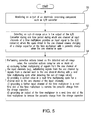
- FIG. 5 shown is a flow chart demonstrating implementation of the various illustrated embodiments. It is noted that the order of steps shown in FIG. 5 is not required, so in principle, the various steps may be performed out of the illustrated order. Also certain steps may be skipped, different steps may be added or substituted, or selected steps or groups of steps may be performed in a separate application following the embodiments described herein.
- a detection logic module of a control system such as one shown in FIG. 3 monitors an output of an electronic processing component such as A/D converter.
- the detection logic module detects an out-of-range value in the output of the A/D converter during one time period during which one channel of input channels of a time multiplexer provides an input signal to the A/D converter; where the open circuit in the one channel causes charging of a charge capacitor of the time multiplexer with a parasitic charge when the one channel is closed.
- a state machine of a control system performs corrective actions based on the detected out-of-range value, whereby the corrective actions comprise one or more of:
Landscapes
- Engineering & Computer Science (AREA)
- Theoretical Computer Science (AREA)
- Analogue/Digital Conversion (AREA)
- Time-Division Multiplex Systems (AREA)
Abstract
Description
- The embodiments described herein relate to a method and apparatus for correcting a time multiplexing channel, and more specifically, to providing an open multiplexer channel charge injection elimination circuit.
- This section is intended to provide a background or context to the embodiments disclosed below. The description herein may include concepts that could be pursued, but are not necessarily ones that have been previously conceived, implemented or described. Therefore, unless otherwise explicitly indicated herein, what is described in this section is not prior art to the description in this application and is not admitted to be prior art by inclusion in this section.
- Many programs utilize analog multiplexers for common signal processing prior to A/D (analog-to-digital) converters. The A/D converters and time (or time division) multiplexers are often controlled by state machines that require little to no software intervention. A state machine can cycle through inputs and after allowing sufficient settling time will start the A/D conversion process. After the A/D conversion is complete the state machine will select the next multiplexer channel to its conversion and go through all signals.
-
FIG. 1 shows an example of aconventional control system 10 comprising a time multiplexer (time division multiplexer) 14, an A/D converter 12 and astate machine 16. Themultiplexer 14 comprises 4 channels with corresponding 4input signals input signal corresponding switch D converter 12 for further processing (analog-to-digital conversion). The timing of opening and closing ofswitches state machine 16 in a cycle manner and typically each channel may be open for a time period from approximately 10 microseconds to 10 millisecond. - In one aspect, the invention provides a method and system for monitoring an output of an electronic processing component which detects an out-of-range value in the output of the electronic processing component during one time period during which one channel of input channels of a time multiplexer provides an input signal to the electronic processing component. Corrective actions are performed based on the detected out-of-range value. The corrective actions consisting of excluding further multiplexing of signals from the one channel of the input channels.
- The accompanying drawings illustrate various non-limiting, illustrative, embodiments in accordance with the present invention:
-
FIG. 1 depicts an example of a control system comprising a time multiplexer, an A/D converter and a state machine (Prior Art); -
FIG. 2 depicts an example of a control system showing an open circuit in one of the input channel of the time multiplexer to be corrected for using exemplary embodiments described herein; -
FIG. 3 depicts an exemplary embodiment of a control system (apparatus) for implementing corrective actions in case of an open circuit in one of the input channels of the time multiplexer; -
FIG. 4 depicts an exemplary embodiment of a state machine states illustrating corrective actions for an open circuit in one of the input channels of the time multiplexer; and -
FIG. 5 depicts a flow chart illustrating implementation of various embodiments. - The present invention is now described more fully with reference to the accompanying drawings, in which illustrated embodiments of the present invention are shown. The present invention is not limited in any way to the illustrated embodiments as the illustrated embodiments described below are merely exemplary of the invention, which can be embodied in various forms, as appreciated by one skilled in the art. Therefore, it is to be understood that any structural and functional details disclosed herein are not to be interpreted as limiting, but merely as a basis for the claims and as a representative for teaching one skilled in the art to variously employ the present invention. Furthermore, the terms and phrases used herein are not intended to be limiting but rather to provide an understandable description of the invention.
- Where a range of values is provided, it is understood that each intervening value, to the tenth of the unit of the lower limit unless the context clearly dictates otherwise, between the upper and lower limit of that range and any other stated or intervening value in that stated range is encompassed within the invention. The upper and lower limits of these smaller ranges may independently be included in the smaller ranges is also encompassed within the invention, subject to any specifically excluded limit in the stated range. Where the stated range includes one or both of the limits, ranges excluding either both of those included limits are also included in the invention.
- Unless defined otherwise, all technical and scientific terms used herein have the same meaning as commonly understood by one of ordinary skill in the art to which this invention belongs. Although any methods and materials similar or equivalent to those described herein can also be used in the practice or testing of the present invention, exemplary methods and materials are now described.
- It must be noted that as used herein and in the appended claims, the singular forms "a", "an," and "the" include plural referents unless the context clearly dictates otherwise. Thus, for example, reference to "a stimulus" includes a plurality of such stimuli and reference to "the signal" includes reference to one or more signals and equivalents thereof known to those skilled in the art, and so forth.
- In regard to the drawings (
FIGS. 1-5 ) presented herein, similar reference characters/numbers denote similar elements throughout the drawings. - It is to be understood and appreciated that often normal input operating voltages into the time multiplexers (such as the one shown in
FIG. 1 ) are far smaller than the values seen for open inputs. Large voltages can exist on inputs under open circuit conditions resulting in charging up parasitic capacitances in multiplexers. - This is demonstrated in
FIG. 2 where an open line (open channel) 17 corresponding to theinput signal 20b (input/channel B) would charge the capacitor 26 (CCharge) up to 10V of a DCbiasing power source 15 when theswitch 24b is open. Then an output value generated by an A/D converter 12 for the channel B would be large (out-of scale) in the output of the A/D converter. Moreover, when themultiplexer 14 is switched to a next channel corresponding to theinput signal 20c (input C) by opening theswitch 24c, this charge stored in the capacitor 26 (CCharge) may inject an offset noise into the signal of the channel C during time theswitch 24c is open, which may cause an error in the A/D converted output for the channel C. In other words, in the example shown inFIG. 2 with open circuit in channel B, theinput 20c (input C) may then be read to be larger than expected due to this charge transfer from the open input B when theswitch 24b was open. - Some recent programs have utilized common software for Input/Output (IO) processing even though all the I/O of the programs are not the same. This results in inputs to the multiplexer intentionally remaining open. For instance, when an input is opened in use, the subsequent input converted by the A/D after that opened input has an error term added from the charge injection. The solution was to force the A/D to read a ground input between every conversion which consumed A/D conversion time even though data from the grounded input was not used. In many cases this is not feasible due to throughput and timing requirements. Additionally, the dual use application program resulted in compiling unique IO software because the IO logic could not automatically manage the unused input interface (channel) in the time multiplexer.
- It is to be appreciated that these approaches are costly and/or cause performance degradation. It is thus desirable to overcome the aforementioned drawbacks by effectively managing open input/channel in the time multiplexer, which is disclosed in the various exemplary embodiments described herein.
- A method, apparatus/system and software related product (e.g., a computer readable memory) are presented for providing an open multiplexer channel charge injection elimination circuit. One embodiment comprises monitoring an output of an electronic processing component such as A/D converter, and detecting an out-of range value in the output of that electronic processing component such as A/D converter during one time period during which one channel of input channels (e.g., analog input channels) of a time multiplexer provides an input signal to the electronic processing component (A/D converter). This may follow by performing corrective actions based on the detected out-of-range value. The corrective actions are further described below but comprise at least excluding further multiplexing of signals from the one channel (having the open circuit) identified using this determined out-of scale value.
- It is appreciated and understood that the out-of-range value may be caused by an open circuit in the one channel (such as channel B in
FIG. 2 ) of the input channels of the time multiplexer, such that the open circuit in the one channel causes charging of a charge capacitor of the time multiplexer with a parasitic charge when the one channel is open, so that the parasitic charge may negatively affect reading in time domain of a channel (such as channel with input C inFIG. 2 ) next to the one channel (channel with input B) of the input channels. - Corrective actions may further include providing a correct value in a next time multiplexing cycle for a channel next to the one channel of the input channels as further discussed in reference to
FIGS. 3 and4 below. In further embodiments, after detecting one of the input channels to be defective (having an open circuit) based on determining the an out-of-range value, and before processing by the electronic processing component (A/D converter) an input of a channel next to the one channel, the corrective actions may include the below discussed actions. -
FIG. 3 shows an exemplary embodiment of a control system (device or apparatus) 100 for implementing corrective actions in case of an open circuit in one of the input channels of thetime multiplexer 14. Thesystem 100 comprises a multiplexer 14a, an A/D converter 12, adetection logic module 28, astate machine 16a, aprocessor 32 and at least onememory 30. Themultiplexer 14, and A/D converter 12 may be parts of the system/apparatus 100 or may be separate blocks/modules.Figure 3 is a simplified block diagram of various components that are suitable for practicing the exemplary embodiments, and a specific manner in which components are configured to cause that control system to operate. - According to an exemplary embodiment, a detection logic module (digital processing block) 28 is added to monitor the converted A/D values to detect an out-of scale value and therefore to determine if any of the input channels (with
corresponding input signals - The
module 28 may be implemented as an application computer program stored in thememory 30, but in general it may be implemented as software, firmware and/or hardware module or a combination thereof. In particular, in the case of software or firmware, one embodiment may be implemented using a software related product such as a computer readable memory (e.g., non-transitory computer readable memory), computer readable medium or a computer readable storage structure comprising computer readable instructions (e.g., program instructions) using a computer program code (i.e., the software or firmware) thereon to be executed by a computer processor. Furthermore, themodule 28 may be implemented as a separate block or may be combined with any other module/block of the system/apparatus 100, or it may be split into several blocks according to their functionality. - After detecting an open input in one of the input channels by the
detection logic module 28, thestate machine 16a may be modified, using an input/command from thedetection logic module 28 to take corrective actions by providing appropriate commands to themultiplexer 14. The correcting actions may include at least excluding further multiplexing of signals from the one channel (having the open circuit) identified using this determined out-of scale value, and eliminating errors in the channel next (in time domain) to this defective channel having the open circuit as described above and further discussed in reference toFIGS. 4 and5 . - Thus, it is appreciated and understood that the open circuit input channel would then have no effect on subsequent A/D conversion due to the charge injection in the
capacitor 26, which is eliminated using the embodiments described herein. Also, as software (for example stored in the memory 30) would be able to read the status of which channel/interface is considered open, it may also force the state machine to restart and verify (for example, using the module 28) that the out of range inputs are still out of range if needed. - It is to be appreciated that the
state machine 16a may be implemented as a hardware module such as a field programmable gate array (FPGA). Alternatively, thestate machine 16a may be implemented as an application computer program, for example stored in thememory 30, but in general it may be implemented as software, firmware and/or hardware module or a combination thereof. In particular, in the case of software or firmware, one embodiment may be implemented using a software related product such as a computer readable memory (e.g., non-transitory computer readable memory), computer readable medium or a computer readable storage structure comprising computer readable instructions (e.g., program instructions) using a computer program code (i.e., the software or firmware) thereon to be executed by a computer processor. Furthermore, thestate machine 16a may be implemented as a separate block or may be combined with any other module/block of the system/apparatus 100, or it may be split into several blocks according to their functionality. - Various embodiments of the at least one memory 30 (e.g., computer readable memory) may include any data storage technology type which is suitable to the local technical environment, including but not limited to semiconductor based memory devices, magnetic memory devices and systems, optical memory devices and systems, fixed memory, removable memory, disc memory, flash memory, DRAM, SRAM, EEPROM and the like. Various embodiments of the
processor 32 may include but are not limited to, general purpose computers, special purpose computers, microprocessors, digital signal processors (DSPs) and multi-core processors. -
FIG. 4 depicts an embodiment of state machine states illustrating corrective actions for an open circuit in one of the input channels of the time multiplexer. InFIG. 4 it is determined (for example by themodule 28 ofFIG. 3 ) that the channel B has an open value (out-of range value in the output of the A/D converter 12) during atime slot 37a. - The corrective action in
FIG. 4 comprises a realization that the value read on channel C during atime slot 37b may have an error due to the charging thecapacitor 26 during thetime slot 37a and therefore the value of channel C during thetime slot 37b may be discarded. Then in a next time multiplexing cycle during atime slot 37c (which corresponds to the defective/open channel B), instead of closing theswitch 24b of the channel B, the state machine closes theswitch 24c for the channel C, which is repeated during thetime slot 37d. The value of Vc provided to the A/D converter for the channel C during thetime slot 37d this is a correct value. The value Vc during thetime slot 37c (which may be a correct value as well) is not used (which may be discarded). It is noted Vc is the voltage at the input to the A/D, which should also be the output from the A/D. - With reference now to
FIG. 5 , shown is a flow chart demonstrating implementation of the various illustrated embodiments. It is noted that the order of steps shown inFIG. 5 is not required, so in principle, the various steps may be performed out of the illustrated order. Also certain steps may be skipped, different steps may be added or substituted, or selected steps or groups of steps may be performed in a separate application following the embodiments described herein. - In a method according to the embodiment shown in
FIG. 5 , in afirst step 50, a detection logic module of a control system (apparatus) such as one shown inFIG. 3 monitors an output of an electronic processing component such as A/D converter. - In a
next step 52, the detection logic module detects an out-of-range value in the output of the A/D converter during one time period during which one channel of input channels of a time multiplexer provides an input signal to the A/D converter; where the open circuit in the one channel causes charging of a charge capacitor of the time multiplexer with a parasitic charge when the one channel is closed. - In a
next step 54, a state machine of a control system (apparatus) performs corrective actions based on the detected out-of-range value, whereby the corrective actions comprise one or more of: - a) excluding further multiplexing of signals from the one channel of the input channels (e.g., substituting signals from the one channel by signals from a channel next to the one channel starting with a next time multiplexing cycle after detecting the out-of-range value);
- b) providing a correct value in a next time multiplexing cycle for a channel next to the one channel of the input channels;
- c) grounding a further input channel of the time multiplexer in a next time slot of the time multiplexer to remove the parasitic charge from the charge capacitor; and
- d) grounding an output of the time multiplexer in a next time slot of the time multiplexer to remove the parasitic charge from the charge capacitor.
- It is noted that various non-limiting embodiments described herein may be used separately, combined or selectively combined for specific applications.
- Further, some of the various features of the above non-limiting embodiments may be used to advantage without the corresponding use of other described features. The foregoing description should therefore be considered as merely illustrative of the principles, teachings and exemplary embodiments of this invention, and not in limitation thereof.
- It is to be understood that the above-described arrangements are only illustrative of the application of the principles of the present invention. Numerous modifications and alternative arrangements may be devised by those skilled in the art without departing from the scope of the invention, and the appended claims are intended to cover such modifications and arrangements.
Claims (15)
- A method, comprising:monitoring an output of an electronic processing component (12);detecting an out-of-range value in the output of the electronic processing component during one time period during which one channel of input channels of a time multiplexer (14) provides an input signal to the electronic processing component; andperforming corrective actions based on the detected out-of-range value, the corrective actions comprising at least excluding further multiplexing of signals from the one channel of the input channels.
- The method of claim 1, wherein the electronic processing component is an analog-to-digital convertor (12) and the input channels are analog input channels.
- The method of claim 1 or 2, wherein the out-of-range value is caused by an open circuit (17) in the one channel of the input channels of the time multiplexer; and preferably wherein the open circuit in the one channel causes charging of a charge capacitor (26) of the time multiplexer with a parasitic charge when the one channel is open, so that the parasitic charge negatively affects reading in time domain of a next converted channel in time to the one channel of the input channels.
- The method of claim 1, 2 or 3 wherein excluding further multiplexing of signals from the one channel of the input channels comprises substituting signals from the one channel by signals from a channel next to the one channel starting with a next time multiplexing cycle after detecting the out-of-range value.
- The method of any preceding claim, wherein the corrective actions further comprise:providing a correct value in a next time multiplexing cycle for a channel next to the one channel of the input channels.
- An apparatus (100), comprising:at least one processor (32) and a memory (30) storing a set of computer instructions, in which the processor and the memory storing the computer instructions are configured to cause the apparatus to:monitor an output of an electronic processing component (12);detect an out-of-range value in the output of the electronic processing component during one time period during which one channel of input channels of a time multiplexer (14) provides an input signal to the electronic processing component; andperform corrective actions based on the detected out-of-range value, the corrective actions comprise at least excluding further multiplexing of signals from the one channel of the input channels.
- The apparatus of claim 6, wherein the electronic processing component is an analog-to-digital convertor (12) and the input channels are analog input channels.
- The apparatus of claim 6 or 7, wherein the out-of-range value is caused by an open circuit (17) in the one channel of the input channels of the time multiplexer; and preferably wherein the open circuit in the one channel causes charging of a charge capacitor (26) of the time multiplexer with a parasitic charge when the one channel is open, so that the parasitic charge negatively affects reading in time domain of a channel next to the one channel of the input channels.
- An apparatus (100), comprising:a detection logic module (26) configured to monitor an output of an electronic processing component (12) and to detect an out-of-range value in the output of the electronic processing component during one time period during which one channel of input channels of a time multiplexer (14) provides an input signal to the electronic processing component; anda control module (16a), configured to perform corrective actions based on the detected out-of-range value, the corrective actions comprise at least excluding further multiplexing of signals from the one channel of the input channels.
- The apparatus of claim 9, wherein the control module comprises a field programmable gate array; and/or wherein the control module comprises a state machine.
- The apparatus of claim 9 or 10, wherein the electronic processing component is an analog-to-digital convertor (12) and the input channels are analog input channels.
- The apparatus of claim 9, 10 or 11, wherein the out-of-range value is caused by an open circuit (17) in the one channel of the input channels of the time multiplexer; and preferably wherein the open circuit in the one channel causes charging of a charge capacitor of the time multiplexer with a parasitic charge when the one channel is open, so that the parasitic charge negatively affects reading in time domain of a channel next to the one channel of the input channels.
- A computer program product comprising a non-transitory computer readable medium bearing computer program code embodied therein for use with a computer, the computer program code comprising:code for monitoring an output of an electronic processing component;code for detecting an out-of-range value in the output of the electronic processing component during one time period during which one channel of input channels of a time multiplexer provides an input signal to the electronic processing component; andcode for performing corrective actions based on the detected out-of-range value, the corrective actions comprise at least excluding further multiplexing of signals from the one channel of the input channels.
- The computer program product method of claim 13, wherein the electronic processing component is an analog-to-digital convertor and the input channels are analog input channels.
- The computer program product method of claim 13 or 14, wherein the out-of-range value is caused by an open circuit in the one channel of the input channels of the time multiplexer; and preferably wherein the open circuit in the one channel causes charging of a charge capacitor of the time multiplexer with a parasitic charge when the one channel is open, so that the parasitic charge negatively affects reading in time domain of a channel next to the one channel of the input channels.
Applications Claiming Priority (1)
| Application Number | Priority Date | Filing Date | Title |
|---|---|---|---|
| US13/898,216 US8854241B1 (en) | 2013-05-20 | 2013-05-20 | Time multiplexer channel corrections |
Publications (2)
| Publication Number | Publication Date |
|---|---|
| EP2806564A2 true EP2806564A2 (en) | 2014-11-26 |
| EP2806564A3 EP2806564A3 (en) | 2015-01-14 |
Family
ID=50842040
Family Applications (1)
| Application Number | Title | Priority Date | Filing Date |
|---|---|---|---|
| EP14169124.6A Ceased EP2806564A3 (en) | 2013-05-20 | 2014-05-20 | Time multiplexer channel corrections |
Country Status (2)
| Country | Link |
|---|---|
| US (1) | US8854241B1 (en) |
| EP (1) | EP2806564A3 (en) |
Citations (2)
| Publication number | Priority date | Publication date | Assignee | Title |
|---|---|---|---|---|
| WO2012069871A1 (en) * | 2010-11-22 | 2012-05-31 | Freescale Semiconductor, Inc. | Integrated circuit device and method for detecting an excessive voltage state |
| US20120176141A1 (en) * | 2011-01-11 | 2012-07-12 | Denso Corporation | Signal input circuit and integrated circuit |
Family Cites Families (11)
| Publication number | Priority date | Publication date | Assignee | Title |
|---|---|---|---|---|
| US5661422A (en) * | 1995-12-12 | 1997-08-26 | Analog Devices, Inc. | High speed saturation prevention for saturable circuit elements |
| US6124820A (en) * | 1997-11-20 | 2000-09-26 | National Semiconductor Corporation | Error correction architecture for pipeline analog to digital converters |
| US6219817B1 (en) * | 1998-04-20 | 2001-04-17 | Intel Corporation | Error correction and detection for faults on time multiplexed data lines |
| US6351231B1 (en) * | 1999-12-23 | 2002-02-26 | Analog Devices, Inc. | Successive approximation analogue-to-digital converter |
| JP2003258639A (en) * | 2002-02-27 | 2003-09-12 | Nec Microsystems Ltd | Analog-to-digital converter |
| US6946984B2 (en) * | 2002-04-10 | 2005-09-20 | Systel Development And Industries Ltd. | System on chip for digital control of electronic power devices |
| US7237172B2 (en) * | 2002-12-24 | 2007-06-26 | Micron Technology, Inc. | Error detection and correction in a CAM |
| JP4593396B2 (en) * | 2005-08-02 | 2010-12-08 | 株式会社日立製作所 | Mobile communication system |
| US7746785B2 (en) * | 2005-08-22 | 2010-06-29 | Broadcom Corporation | Time multiplexing logic in physical design domain for multiple instantiation |
| US7839194B2 (en) * | 2007-11-21 | 2010-11-23 | Rambus Inc. | Clock circuitry for generating multiple clocks with time-multiplexed duty cycle adjustment |
| JP5684599B2 (en) * | 2011-02-18 | 2015-03-11 | ルネサスエレクトロニクス株式会社 | Semiconductor integrated circuit device |
-
2013
- 2013-05-20 US US13/898,216 patent/US8854241B1/en active Active
-
2014
- 2014-05-20 EP EP14169124.6A patent/EP2806564A3/en not_active Ceased
Patent Citations (2)
| Publication number | Priority date | Publication date | Assignee | Title |
|---|---|---|---|---|
| WO2012069871A1 (en) * | 2010-11-22 | 2012-05-31 | Freescale Semiconductor, Inc. | Integrated circuit device and method for detecting an excessive voltage state |
| US20120176141A1 (en) * | 2011-01-11 | 2012-07-12 | Denso Corporation | Signal input circuit and integrated circuit |
Non-Patent Citations (1)
| Title |
|---|
| TEXAS INSTRUMENTS: "ADS1158 - 16-Channel, 16-Bit Analog-to-Digital Converter", 17 March 2011 (2011-03-17), pages 1 - 52, XP055365635, Retrieved from the Internet <URL:http://www.ti.com/lit/ds/symlink/ads1158.pdf> [retrieved on 20170419] * |
Also Published As
| Publication number | Publication date |
|---|---|
| US8854241B1 (en) | 2014-10-07 |
| EP2806564A3 (en) | 2015-01-14 |
Similar Documents
| Publication | Publication Date | Title |
|---|---|---|
| US9202591B2 (en) | On-line memory testing systems and methods | |
| US9418000B2 (en) | Dynamically compensating for degradation of a non-volatile memory device | |
| US9947283B2 (en) | Display apparatus with testing functions and driving circuit and driving method thereof | |
| US11131706B2 (en) | Degradation monitoring of semiconductor chips | |
| US9298253B2 (en) | Accelerating the microprocessor core wakeup by predictively executing a subset of the power-up sequence | |
| JP2019511730A (en) | Self-referenced on-die voltage drop detector | |
| US10073800B2 (en) | Coupling controller, information processing apparatus and coupling control method | |
| DE112017005007T5 (en) | system monitor | |
| US20150063021A1 (en) | Memory controller for reducing capacitive coupling in a cross-point memory | |
| US10127871B2 (en) | Liquid crystal display device including a detection circuit | |
| CN105045713A (en) | Data processing method and mobile terminal | |
| US20210191538A1 (en) | Capacitance compensation module and method, self-capacitive touch display panel and display device | |
| JP2014175895A (en) | Balanced signal processing circuit and analog-digital conversion circuit | |
| KR20180006905A (en) | Analog-to-Digital Converter with Internal Timer | |
| CN103049599A (en) | Global clock handler object for HDL environment | |
| US20180039323A1 (en) | Power supply control | |
| US8854241B1 (en) | Time multiplexer channel corrections | |
| US9281079B2 (en) | Dynamic hard error detection | |
| US10054634B2 (en) | Test device | |
| US11715545B2 (en) | In-system test of a memory device | |
| US9720026B1 (en) | Radiation hardened chip level integrated recovery apparatus, methods, and integrated circuits | |
| KR101560493B1 (en) | Output device and diagnosis method thereof | |
| EP3422581B1 (en) | Correlated double sampling integrating circuit | |
| US9537506B2 (en) | Electronic device with keys and voltage detecting method thereof | |
| DE112023001803T5 (en) | OPERATING VOLTAGE OF A SEMICONDUCTOR UNIT |
Legal Events
| Date | Code | Title | Description |
|---|---|---|---|
| PUAI | Public reference made under article 153(3) epc to a published international application that has entered the european phase |
Free format text: ORIGINAL CODE: 0009012 |
|
| 17P | Request for examination filed |
Effective date: 20140520 |
|
| AK | Designated contracting states |
Kind code of ref document: A2 Designated state(s): AL AT BE BG CH CY CZ DE DK EE ES FI FR GB GR HR HU IE IS IT LI LT LU LV MC MK MT NL NO PL PT RO RS SE SI SK SM TR |
|
| AX | Request for extension of the european patent |
Extension state: BA ME |
|
| PUAL | Search report despatched |
Free format text: ORIGINAL CODE: 0009013 |
|
| AK | Designated contracting states |
Kind code of ref document: A3 Designated state(s): AL AT BE BG CH CY CZ DE DK EE ES FI FR GB GR HR HU IE IS IT LI LT LU LV MC MK MT NL NO PL PT RO RS SE SI SK SM TR |
|
| AX | Request for extension of the european patent |
Extension state: BA ME |
|
| RIC1 | Information provided on ipc code assigned before grant |
Ipc: H03M 1/12 20060101AFI20141211BHEP |
|
| R17P | Request for examination filed (corrected) |
Effective date: 20150619 |
|
| RBV | Designated contracting states (corrected) |
Designated state(s): AL AT BE BG CH CY CZ DE DK EE ES FI FR GB GR HR HU IE IS IT LI LT LU LV MC MK MT NL NO PL PT RO RS SE SI SK SM TR |
|
| STAA | Information on the status of an ep patent application or granted ep patent |
Free format text: STATUS: EXAMINATION IS IN PROGRESS |
|
| 17Q | First examination report despatched |
Effective date: 20170502 |
|
| APBK | Appeal reference recorded |
Free format text: ORIGINAL CODE: EPIDOSNREFNE |
|
| APBN | Date of receipt of notice of appeal recorded |
Free format text: ORIGINAL CODE: EPIDOSNNOA2E |
|
| APBR | Date of receipt of statement of grounds of appeal recorded |
Free format text: ORIGINAL CODE: EPIDOSNNOA3E |
|
| APAF | Appeal reference modified |
Free format text: ORIGINAL CODE: EPIDOSCREFNE |
|
| APAF | Appeal reference modified |
Free format text: ORIGINAL CODE: EPIDOSCREFNE |
|
| APBT | Appeal procedure closed |
Free format text: ORIGINAL CODE: EPIDOSNNOA9E |
|
| STAA | Information on the status of an ep patent application or granted ep patent |
Free format text: STATUS: THE APPLICATION HAS BEEN REFUSED |
|
| 18R | Application refused |
Effective date: 20220201 |